Embed Size (px)
Citation preview
PCN MMS-MMY/13/7714Dated 18 Feb 2013
M24C01, M24C02, M24C04, M24C16 1-, 2-, 4-, 16-Kbit I2C
Bus EEPROM Industrial grade / UFDFPN8 & TSSOP8 packages
Redesign and upgrade to the CMOSF8H+
1/77
PRODUCT/PROCESSCHANGE NOTIFICATION®
PCN MMS-MMY/13/7714 - Dated 18 Feb 2013
Table 1. Change Implementation ScheduleForecasted implementation date for 11-Feb-2013 change
Forecasted availability date of samples 11-Feb-2013 for customer
Forecasted date for STMicroelectronicschange Qualification Plan results availability 11-Feb-2013
Estimated date of changed product first 20-May-2013 shipment
Table 2. Change IdentificationProduct Identification M24C01 M24C02 M24C04, M24C16 in UFDFPN8 & TSSOP8 (Product Family/Commercial Product)
Type of change Waferfab technology change
Reason for change Line up to state-of-the-art of process
Description of the change Redesign and upgrade to the new CMOSF8H+ process technology.
Change Product Identification Process Technology identifier "T" for CMOSF8H+
Manufacturing Location(s)
® 2/77
PCN MMS-MMY/13/7714 - Dated 18 Feb 2013
DOCUMENT APPROVAL
Name Function
Leduc, Hubert Marketing Manager
Rodrigues, Benoit Product Manager
Malbranche, Jean-Luc Q.A. Manager
® 4/77
M24C01, M24C02, M24C04, M24C16 1-, 2-, 4-, 16-Kbit I2C Bus EEPROM Industrial grade / UFDFPN8 & TSSOP8 packages
Redesign and upgrade to the CMOSF8H + process technology
What is the change? The M24C01, M24C02, M24C04, M24C16, 1-Kbit, 2-Kbit, 4-Kbit, 16-Kbit serial I²C bus EEPROM product families for Industrial grade, assembled in UFDFPN8 and TSSOP8 packages, currently produced using the CMOSF6SP 36% process technology at ST Ang Mo Kio (Singapore) 6” wafer diffusion plant or at GLOBALFOUNDRIES (Singapore) 8” wafer diffusion plant, have been redesigned and will be upgraded to the CMOSF8H+ process technology at ST Rousset (France) 8” wafer diffusion plant. The CMOSF8H+ is closely derived from CMOSF8H (already used for production of densities ranging from 32 Kb to 2 Mb), with a more compact layout, in order to achieve competitive die size.
This upgraded version in CMOSF8H+ allows offering: - 1.7 V / 5.5 V (“-F”) Vcc range
The new M24C01, M24C02, M24C04 and M24C16 in CMOSF8H+ version are functionally compatible with the current CMOSF6SP 36% version as per common datasheet rev. 17 – April 2011, attached.
These new M24C01, M24C02, M24C04 and M24C16 are described in specific datasheets: A common datasheet for both M24C01 and M24C02 (rev. 1, Dec. 2012), a single datasheet for M24C04 (rev. 2, Jan. 2013), a single datasheet for M24C16 (rev. 1, Oct. 2012) with following differences versus previous common datasheet rev. 17:
- DC characteristic: ICC1 standby supply current: - Max 2 µA at VCC = 2.5 V - Max 3 µA at VCC = 5.5 V
- - Absolute maximum rating: VESD electrostatic pulse Human Body model:
- Max 3000 V
Concurrent to this change, the UFDFPN8 and TSSOP8 packages will be assembled with 0.8 mil Copper wire (Copper wire assembly process already qualified and in full production for M24C01, M24C02, M24C04 and M24C16 in CMOSF8H+, when assembled on SO8N SHD line at ST Shenzhen (China)).
Why? The strategy of STMicroelectronics Memory Division is to support our customers on a long-term basis. In line with this commitment, the qualification of the M24C01, M24C02, M24C04 and M24C16 in the new CMOSF8H+ process technology will increase the production capacity throughput and consequently improve the service to our customers.
PRODUCT / PROCESS CHANGE NOTIFICATION

2
M24C01, M24C02, M24C04, M24C16, 1-, 2-, 4-, 16-Kbit I²C Bus EEPROM Industrial grade / UFDFPN8 & TSSOP8 packages
Redesign and upgrade to the CMOSF8H+ process technology
When? The production of the upgraded M24C01, M24C02, M24C04 and M24C16 with the new CMOSF8H+ and assembled in UFDFPN8 and TSSOP8 packages will ramp up from April 2013 and shipments can start from May 2013 onward (or earlier upon customer approval).
How will the change be qualified? The new version of the M24C01, M24C02, M24C04 and M24C16 in CMOSF8H+ and assembled in UFDFPN8 and TSSOP8 packages will be qualified using the standard ST Microelectronics Corporate Procedures for Quality & Reliability. The M24C01, M24C02, M24C04 and M24C16 in SO8N manufactured with the CMOSF8H+ process and assembled in SO8N are already qualified and in full production.
The intermediate Qualification Reports QRMMY1207 (M24C01, M24C02, M24C04) and QRMMY1126 (M24C16) are available and included inside this document.
What is the impact of the change?
- Form: Marking change (see Device marking paragraph)
- Fit: No change
- Function: - Change on DC characteristic ICC1 standby supply current - Change on Absolute maximum rating VESD HBM
3
M24C01, M24C02, M24C04, M24C16, 1-, 2-, 4-, 16-Kbit I²C Bus EEPROM Industrial grade / UFDFPN8 & TSSOP8 packages
Redesign and upgrade to the CMOSF8H+ process technology
How can the change be seen?
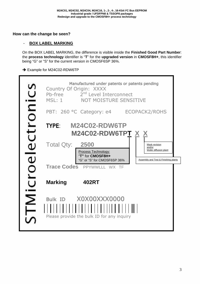
- BOX LABEL MARKING
On the BOX LABEL MARKING, the difference is visible inside the Finished Good Part Number : the process technology identifier is “T” for the upgraded version in CMOSF8H+, this identifier being “G” or “S” for the current version in CMOSF6SP 36%.
� Example for M24C02-RDW6TP
Manufactured under patents or patents pendingManufactured under patents or patents pendingManufactured under patents or patents pendingManufactured under patents or patents pending
Country Of Origin: XXXX Pb-free 2nd Level Interconnect
MSL: 1 NOT MOISTURE SENSITIVE
PBT: 260 °C Category: e4 ECOPACK2/ROHS
TYPE: M24C02-RDW6TP M24C02-RDW6TPT X X
Total Qty: 2500
Trace Codes PPYWWLLL WX TF
Marking 402RT
Bulk IDBulk IDBulk IDBulk ID X0X00XXX0000X0X00XXX0000X0X00XXX0000X0X00XXX0000
Please provide the bulk ID for any inquiry
Process Technology: “T” for CMOSF8H+ “G” or “S” for CMOSF6SP 36% Assembly and Test & Finishing plants
Mask revision and/or Wafer diffusion plant
4
M24C01, M24C02, M24C04, M24C16, 1-, 2-, 4-, 16-Kbit I²C Bus EEPROM Industrial grade / UFDFPN8 & TSSOP8 packages
Redesign and upgrade to the CMOSF8H+ process technology
How can the change be seen?
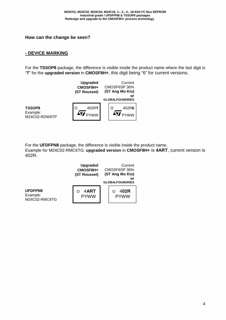
- DEVICE MARKING
For the TSSOP8 package, the difference is visible inside the product name where the last digit is “T” for the upgraded version in CMOSF8H+, this digit being “6” for current versions.
For the UFDFPN8 package, the difference is visible inside the product name. Example for M24C02-RMC6TG: upgraded version in CMOSF8H+ is 4ART, current version is 402R.
Upgraded CMOSF8H+
(ST Rousset)
Current CMOSF6SP 36% (ST Ang Mo Kio)
or GLOBALFOUNDRIES
TSSOP8 Example: M24C02-RDW6TP
O 402RT
PYWW
O 402R6
PYWW
Upgraded CMOSF8H+
(ST Rousset)
Current CMOSF6SP 36% (ST Ang Mo Kio)
or GLOBALFOUNDRIES
UFDFPN8 Example: M24C02-RMC6TG
O 4ART PYWW
O 402R PYWW
5
M24C01, M24C02, M24C04, M24C16, 1-, 2-, 4-, 16-Kbit I²C Bus EEPROM Industrial grade / UFDFPN8 & TSSOP8 packages
Redesign and upgrade to the CMOSF8H+ process technology
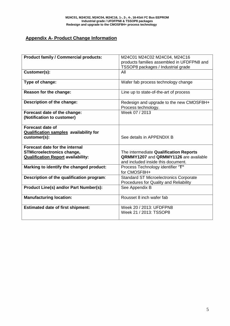
Appendix A- Product Change Information
Product family / Commercial products: M24C01 M24C02 M24C04, M24C16 products families assembled in UFDFPN8 and TSSOP8 packages / Industrial grade
Customer(s): All
Type of change: Wafer fab process technology change
Reason for the change: Line up to state-of-the-art of process
Description o f the change: Redesign and upgrade to the new CMOSF8H+ Process technology.
Forecast date of the change: (Notification to customer)
Week 07 / 2013
Forecast date of Qualification samples availability for customer(s): See details in APPENDIX B
Forecast date for the internal STMicroelectronics change, Qualification Report availability:
The intermediate Qualification Reports QRMMY1207 and QRMMY1126 are available and included inside this document.
Marking to identify the changed product: Process Technology identifier “T” for CMOSF8H+
Description of the qualification program : Standard ST Microelectronics Corporate Procedures for Quality and Reliability
Product Line(s) and/or Part Number(s): See Appendix B
Manufacturing location: Rousset 8 inch wafer fab
Estimated date of first shipment: Week 20 / 2013: UFDFPN8 Week 21 / 2013: TSSOP8
6
M24C01, M24C02, M24C04, M24C16, 1-, 2-, 4-, 16-Kbit I²C Bus EEPROM Industrial grade / UFDFPN8 & TSSOP8 packages
Redesign and upgrade to the CMOSF8H+ process technology
Appendix B: Concerned Commercial Part Numbers:
Commercial Part Numbers
Package Samples availability
M24C01-RDW6TP (*) TSSOP8 Week 10 / 2013
M24C01-WDW6TP TSSOP8 Week 10 / 2013
M24C02-RDW6TP (*) TSSOP8 Week 10 / 2013
M24C02-RMC6TG UFDFPN8 Available
M24C02-RMC6TG/12 UFDFPN8 Available
M24C02-WDW6TP TSSOP8 Week 10 / 2013
M24C04-FDW5TP TSSOP8 Week 15 / 2013
M24C04-FMC5TG UFDFPN8 Week 15 / 2013
M24C04-RDW6TP (*) TSSOP8 Week 10 / 2013
M24C04-RMC6TG UFDFPN8 Available
M24C04-WDW6TP TSSOP8 Week 10 / 2013
M24C16-FDW5TP TSSOP8 Week 10 / 2013
M24C16-FMC5TG UFDFPN8 Week 15 / 2013
M24C16-RDW6TP (*) TSSOP8 Week 10 / 2013
M24C16-RMC6TG UFDFPN8 Available
M24C16-RMC6TG/12 UFDFPN8 Week 15 / 2013
M24C16-WDW6TP TSSOP8 Week 10 / 2013
(*) Following product line rationalization, we recommend customer to use –R version (1.8 V – 5.5 V) when –W (2.5 V – 5.5 V) is used. For instance, M24C02-RDW6TP should be preferred to M24C02-WDW6TP.

7
M24C01, M24C02, M24C04, M24C16, 1-, 2-, 4-, 16-Kbit I²C Bus EEPROM Industrial grade / UFDFPN8 & TSSOP8 packages
Redesign and upgrade to the CMOSF8H+ process technology
Appendix C: Qualification Report s:
See following pages
February 2013 Rev 3 1/14
QRMMY1207Qualification report
New design / M24C04 M24C02 M24C01 using the CMOSF8H+ technology at the Rousset 8” Fab
Reliability / Qualification assessment: Pass
Table 1. Product information
General information
Commercial product
M24C04-FMC5TG
M24C04-FMC6TG
M24C04-FMN6TP
M24C04-RMC6TGM24C04-RMN6TP
M24C04-WMN6TP
M24C02-FMC6TG
M24C02-FMN6TP
M24C02-RMC6TG
M24C02-RMC6TG/12
M24C02-RMN6TPM24C02-WMN6TP
M24C01-RMN6TP
M24C01-WMN6TP
Product descriptionM24C04: 4-Kbit serial I²C bus EEPROM
M24C02: 2-Kbit serial I²C bus EEPROMM24C01: 1-Kbit serial I²C bus EEPROM
Product group MMS
Product division MMY - Memory
Silicon process technology CMOSF8H+
Wafer fabrication location RS8F - ST Rousset 8”, France
Electrical Wafer Sort test plant locationST Rousset, France
ST Toa Payoh, Singapore
Table 2. Package description
Package description Assembly plant location Final test plant location
SO8NST Shenzhen, China ST Shenzhen, China
Subcon Amkor, Philippines Subcon Amkor, Philippines
TSSOP8ST Shenzhen, China ST Shenzhen, China
Subcon Amkor, Philippines Subcon Amkor, Philippines
UFDFPN8 (MLP8)
2 x 3 mm
ST Calamba, Philippines ST Calamba, Philippines
Subcon Amkor, Philippines Subcon Amkor, Philippines
www.st.com
Reliability evaluation overview QRMMY1207
2/14 Rev 3
1 Reliability evaluation overview
1.1 ObjectivesThis qualification report summarizes the results of the reliability trials that were performed to qualify the new design M24C04, M24C02 and M24C01 using the CMOSF8H+ silicon process technology at the ST Rousset 8” diffusion fab.
The CMOSF8H+ is closely derived from CMOSF8H silicon process technology (already used for production of EEPROM densities ranging from 32 Kb to 2 Mb), with a more compact layout, in order to achieve a competitive die size.
The CMOSF8H+ technology is already qualified in the ST Rousset 8” fab using M24C16 as driver product.
The voltage and temperature ranges covered by this document are:
● 2.5 to 5.5 V at –40 to 85 °C for -W devices
● 1.8 to 5.5 V at –40 to 85 °C for -R devices
● 1.7 to 5.5 V at –40 to 85 °C for -F devices
This document serves for the qualification of the named product using the named silicon process technology in the named diffusion plant.
1.2 ConclusionThe new design M24C04, M24C02 and M24C01 using the CMOSF8H+ silicon process technology at the ST Rousset 8” diffusion fab have passed all the reliability requirements and all products described in Table 1 are qualified.
Qualification tests for products assembled in TSSOP8 (not yet listed in Table 1) are ongoing with positive preliminary reliability results.
Refer to Section 3: Reliability test results for details on the test results.
QRMMY1207 Device characteristics
Rev 3 3/14
2 Device characteristics
Device descriptionThe M24C04-x, M24C02-x and M24C01-x devices are I2C-compatible electrically erasable programmable memories (EEPROM). They are organized as 512 / 256 / 128 × 8 bits respectively.
The device behaves as a slave in the I2C protocol, with all memory operations synchronized by the serial clock. Read and Write operations are initiated by a Start condition, generated by the bus master. The Start condition is followed by a device select code and a Read/Write bit (RW) terminated by an acknowledge bit.
When writing data to the memory, the device inserts an acknowledge bit during the 9th bit time, following the bus master’s 8-bit transmission. When data is read by the bus master, the bus master acknowledges the receipt of the data byte in the same way. Data transfers are terminated by a Stop condition after an Ack for Write, and after a NoAck for Read.
Refer to the product datasheet for more details.
Reliability test results QRMMY1207
4/14 Rev 3
3 Reliability test results
This section contains a general description of the reliability evaluation strategy.
The named products are qualified using the standard STMicroelectronics corporate procedures for quality and reliability.
The CMOSF8H+ process technology has been qualified on 3 lots using the driver product M24C16 (refer to qualification report QRMMY1126).
The M24C04/M24C02/M24C01 are designed with the same architecture and technology as the driver product M24C16. Qualification of M24C04/M24C02/M24C01 benefits of the family approach (1 lot).
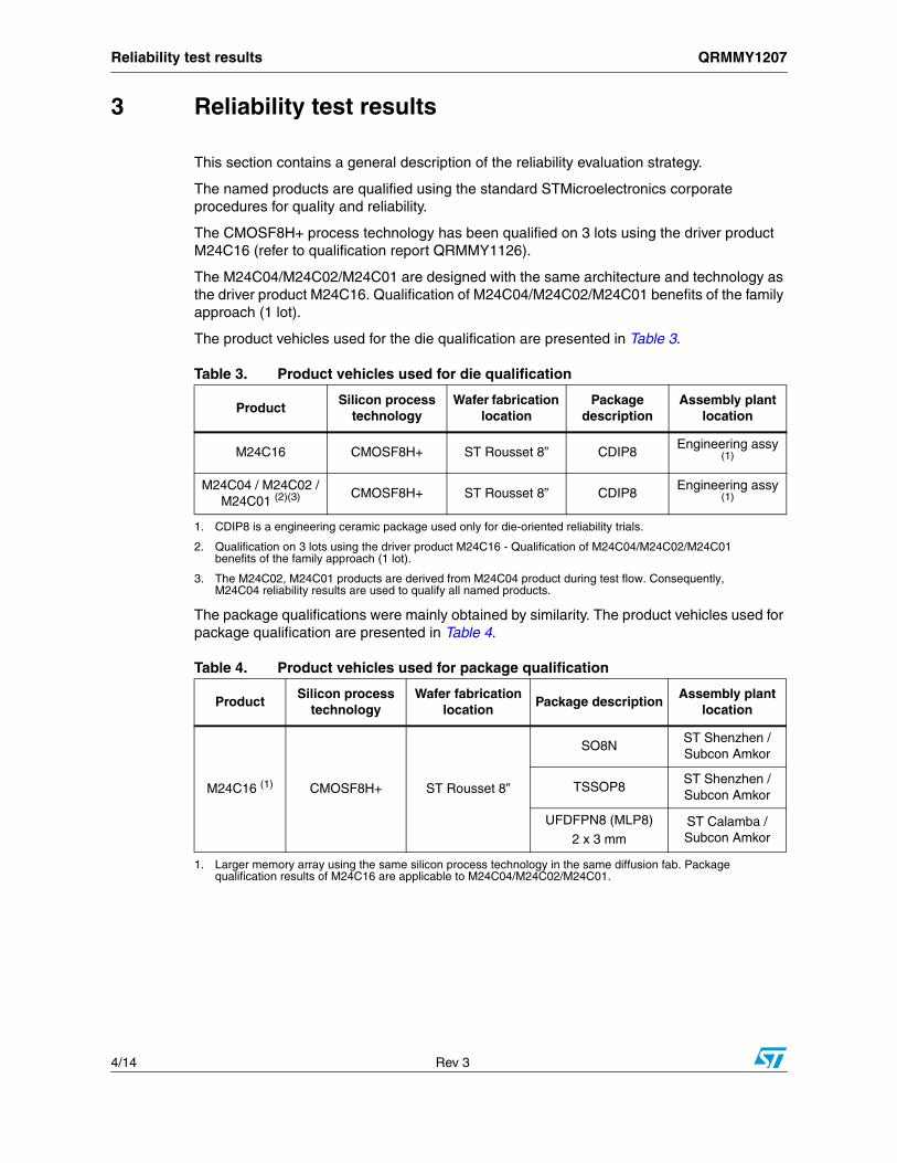
The product vehicles used for the die qualification are presented in Table 3.
The package qualifications were mainly obtained by similarity. The product vehicles used for package qualification are presented in Table 4.
Table 3. Product vehicles used for die qualification
ProductSilicon process
technologyWafer fabrication
locationPackage
descriptionAssembly plant
location
M24C16 CMOSF8H+ ST Rousset 8” CDIP8Engineering assy
(1)
1. CDIP8 is a engineering ceramic package used only for die-oriented reliability trials.
M24C04 / M24C02 / M24C01 (2)(3)
2. Qualification on 3 lots using the driver product M24C16 - Qualification of M24C04/M24C02/M24C01benefits of the family approach (1 lot).
3. The M24C02, M24C01 products are derived from M24C04 product during test flow. Consequently,M24C04 reliability results are used to qualify all named products.
CMOSF8H+ ST Rousset 8” CDIP8Engineering assy
(1)
Table 4. Product vehicles used for package qualification
ProductSilicon process
technologyWafer fabrication
locationPackage description
Assembly plant location
M24C16 (1)
1. Larger memory array using the same silicon process technology in the same diffusion fab. Packagequalification results of M24C16 are applicable to M24C04/M24C02/M24C01.
CMOSF8H+ ST Rousset 8”
SO8NST Shenzhen / Subcon Amkor
TSSOP8ST Shenzhen / Subcon Amkor
UFDFPN8 (MLP8)
2 x 3 mmST Calamba / Subcon Amkor
QRMMY1207 Reliability test results
Rev 3 5/14
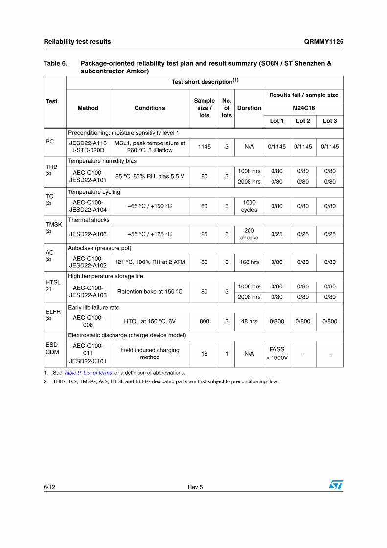
3.1 Reliability test plan and result summaryThe reliability test plan and the result summary are presented as follows:
● in Table 5 for die-oriented tests.
● in Table 6 for SO8N ST Shenzhen / subcontractor Amkor package-oriented tests.
● in Table 7 for TSSOP8 ST Shenzhen / subcontractor Amkor package-oriented tests.
● in Table 8 for UFDFPN8 (MLP8) 2 x 3 mm ST Calamba / subcontractor Amkorpackage-oriented tests.
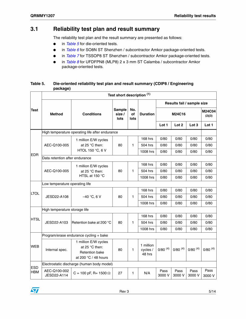
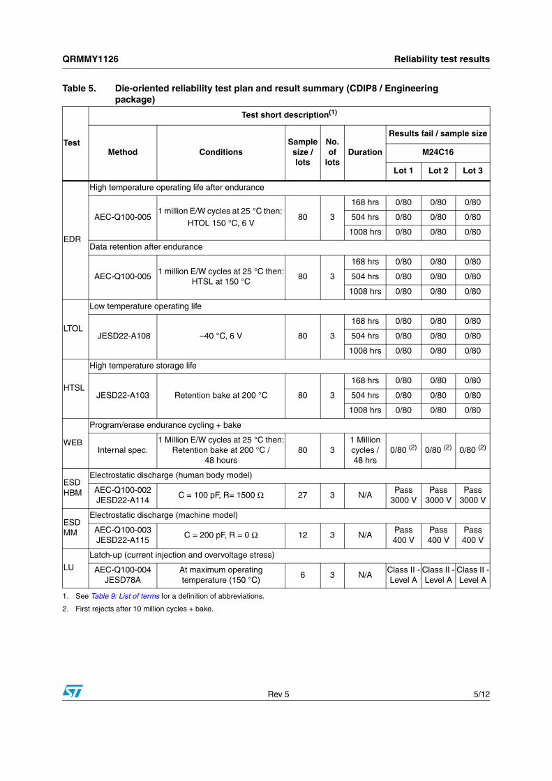
Table 5. Die-oriented reliability test plan and result summary (CDIP8 / Engineering package)
Test
Test short description (1)
Method ConditionsSample size / lots
No. of
lotsDuration
Results fail / sample size
M24C16M24C04
(2)(3)
Lot 1 Lot 2 Lot 3 Lot 1
EDR
High temperature operating life after endurance
AEC-Q100-005
1 million E/W cycles
at 25 °C then: HTOL 150 °C, 6 V
80 1
168 hrs 0/80 0/80 0/80 0/80
504 hrs 0/80 0/80 0/80 0/80
1008 hrs 0/80 0/80 0/80 0/80
Data retention after endurance
AEC-Q100-0051 million E/W cycles
at 25 °C then:HTSL at 150 °C
80 1
168 hrs 0/80 0/80 0/80 0/80
504 hrs 0/80 0/80 0/80 0/80
1008 hrs 0/80 0/80 0/80 0/80
LTOL
Low temperature operating life
JESD22-A108 –40 °C, 6 V 80 1
168 hrs 0/80 0/80 0/80 0/80
504 hrs 0/80 0/80 0/80 0/80
1008 hrs 0/80 0/80 0/80 0/80
HTSL
High temperature storage life
JESD22-A103 Retention bake at 200 °C 80 1
168 hrs 0/80 0/80 0/80 0/80
504 hrs 0/80 0/80 0/80 0/80
1008 hrs 0/80 0/80 0/80 0/80
WEB
Program/erase endurance cycling + bake
Internal spec.
1 million E/W cycles
at 25 °C then:Retention bake
at 200 °C / 48 hours
80 11 million cycles /48 hrs
0/80 (4) 0/80 (4) 0/80 (4) 0/80 (4)
ESD HBM
Electrostatic discharge (human body model)
AEC-Q100-002JESD22-A114
C = 100 pF, R= 1500 27 1 N/APass
3000 VPass
3000 VPass
3000 VPass
3000 V
Reliability test results QRMMY1207
6/14 Rev 3
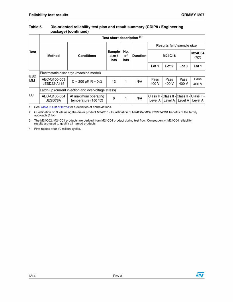
ESD MM
Electrostatic discharge (machine model)
AEC-Q100-003JESD22-A115
C = 200 pF, R = 0 12 1 N/APass400 V
Pass400 V
Pass400 V
Pass 400 V
LU
Latch-up (current injection and overvoltage stress)
AEC-Q100-004JESD78A
At maximum operating temperature (150 °C)
6 1 N/AClass II -Level A
Class II -Level A
Class II -Level A
Class II -Level A
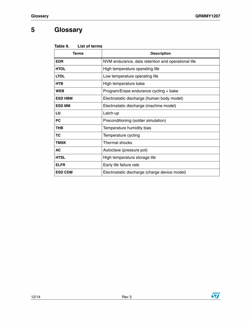
1. See Table 9: List of terms for a definition of abbreviations.
2. Qualification on 3 lots using the driver product M24C16 - Qualification of M24C04/M24C02/M24C01 benefits of the familyapproach (1 lot).
3. The M24C02, M24C01 products are derived from M24C04 product during test flow. Consequently, M24C04 reliabilityresults are used to qualify all named products.
4. First rejects after 10 million cycles.
Table 5. Die-oriented reliability test plan and result summary (CDIP8 / Engineering package) (continued)
Test
Test short description (1)
Method ConditionsSample size / lots
No. of
lotsDuration
Results fail / sample size
M24C16M24C04
(2)(3)
Lot 1 Lot 2 Lot 3 Lot 1
QRMMY1207 Reliability test results
Rev 3 7/14
Table 6. Package-oriented reliability test plan and result summary (SO8N / ST Shenzhen & subcontractor Amkor)
Test
Test short description(1)
Method ConditionsSample size / lots
No. of
lotsDuration
Results fail / sample size
M24C16
M24C04M24C02M24C01
(2)
Lot 1 Lot 2 Lot 3 Lot 1
PC
Preconditioning: moisture sensitivity level 1
JESD22-A113J-STD-020D
MSL1, peak temperature at 260 °C, 3
IReflow1145 1 N/A 0/1145 0/1145 0/1145 -
THB(3)
Temperature humidity bias
AEC-Q100-JESD22-A101
85 °C, 85% RH, bias 5.5 V
80 11008 hrs 0/80 0/80 0/80 -
2008 hrs 0/80 0/80 0/80 -
TC (3)
Temperature cycling
AEC-Q100-JESD22-A104
–65 °C / +150 °C 80 11000 cycles
0/80 0/80 0/80 -
TMSK(3)
Thermal shocks
JESD22-A106 –55 °C / +125 °C 25 1200
shocks0/25 0/25 0/25 -
AC (3)
Autoclave (pressure pot)
AEC-Q100-JESD22-A102
121 °C, 100% RH
at 2 ATM80 1 168 hrs 0/80 0/80 0/80 -
HTSL(3)
High temperature storage life
AEC-Q100-JESD22-A103
Retention bake
at 150 °C80 1
1008 hrs 0/80 0/80 0/80 -
2008 hrs 0/80 0/80 0/80 -
ELFR(3)
Early life failure rate
AEC-Q100-008
HTOL at 150 °C, 6V 800 1 48 hrs 0/800 0/800 0/800 -
ESD CDM
Electrostatic discharge (charge device model)
AEC-Q100-011
JESD22-C101
Field induced charging method
18 1 N/APASS
> 1500V- -
PASS > 1500V
1. See Table 9: List of terms for a definition of abbreviations.
2. Larger memory array using the same silicon process technology in the same diffusion fab - Package qualification results ofM24C16 are applicable to M24C04/M24C02/M24C01.
3. THB-, TC-, TMSK-, AC-, HTSL and ELFR- dedicated parts are first subject to preconditioning flow.
Reliability test results QRMMY1207
8/14 Rev 3
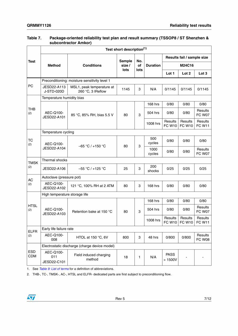
Table 7. Package-oriented reliability test plan and result summary (TSSOP8 / ST Shenzhen & subcontractor Amkor)
Test
Test short description(1)
Method ConditionsSample size / lots
No. of
lotsDuration
Results fail / sample size
M24C16
M24C04M24C02M24C01
(2)
Lot 1 Lot 2 Lot 3 Lot 1
PC
Preconditioning: moisture sensitivity level 1
JESD22-A113J-STD-020D
MSL1, peak temperature at
260 °C, 3 IReflow1145 1 N/A 0/1145 0/1145 0/1145 -
THB(3)
Temperature humidity bias
AEC-Q100-JESD22-A101
85 °C, 85% RH, bias 5.5 V
80 1
168 hrs 0/80 0/80 0/80 -
504 hrs 0/80 0/80Results FC W07
-
1008 hrsResults FC W10
Results FC
W10
Results FC W11
-
TC (3)
Temperature cycling
AEC-Q100-JESD22-A104
–65 °C / +150 °C 80 1
500 cycles
0/80 0/80 0/80 -
1000 cycles
0/80 0/80Results FC W07
-
TMSK(3)
Thermal shocks
JESD22-A106 –55 °C / +125 °C 25 1200
shocks0/25 0/25 0/25 -
AC (3)
Autoclave (pressure pot)
AEC-Q100-JESD22-A102
121 °C, 100% RH at 2 ATM
80 1 168 hrs 0/80 0/80 0/80 -
HTSL(3)
High temperature storage life
AEC-Q100-JESD22-A103
Retention bake at 150 °C
80 1
168 hrs 0/80 0/80 0/80 -
504 hrs 0/80 0/80Results FC W07
-
1008 hrsResults FC W10
Results FC
W10
Results FC W11
-
ELFR(3)
Early life failure rate
AEC-Q100-008HTOL at 150 °C,
6V800 1 48 hrs 0/800 0/800
Results FC W08
-
QRMMY1207 Reliability test results
Rev 3 9/14
ESD CDM
Electrostatic discharge (charge device model)
AEC-Q100-011
JESD22-C101Field induced
charging method18 1 N/A
PASS
> 1500V- -
Results FC W11
1. See Table 9: List of terms for a definition of abbreviations.
2. Larger memory array using the same silicon process technology in the same diffusion fab - Package qualification results ofM24C16 are applicable to M24C04/M24C02/M24C01.
3. THB-, TC-, TMSK-, AC-, HTSL and ELFR- dedicated parts are first subject to preconditioning flow.
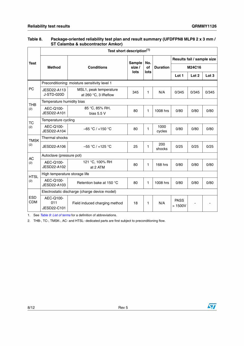
Table 8. Package-oriented reliability test plan and result summary (UFDFPN8 MLP8 2 x 3 mm / ST Calamba & subcontractor Amkor)
Test
Test short description(1)
Method ConditionsSample size / lots
No. of
lotsDuration
Results fail / sample size
M24C16
M24C04M24C02M24C01
(2)
Lot 1 Lot 2 Lot 3 Lot 1
PC
Preconditioning: moisture sensitivity level 1
JESD22-A113J-STD-020D
MSL1, peak temperature at 260 °C, 3
IReflow345 1 N/A 0/345 0/345 0/345 -
THB(3)
Temperature humidity bias
AEC-Q100-JESD22-A101
85 °C, 85% RH,
bias 5.5 V80 1 1008 hrs 0/80 0/80 0/80 -
TC (3)
Temperature cycling
AEC-Q100-JESD22-A104
–65 °C / +150 °C 80 11000 cycles
0/80 0/80 0/80 -
TMSK(3)
Thermal shocks
JESD22-A106 –55 °C / +125 °C 25 1200
shocks0/25 0/25 0/25 -
Table 7. Package-oriented reliability test plan and result summary (TSSOP8 / ST Shenzhen & subcontractor Amkor) (continued)
Test
Test short description(1)
Method ConditionsSample size / lots
No. of
lotsDuration
Results fail / sample size
M24C16
M24C04M24C02M24C01
(2)
Lot 1 Lot 2 Lot 3 Lot 1
Reliability test results QRMMY1207
10/14 Rev 3
AC (3)
Autoclave (pressure pot)
AEC-Q100-JESD22-A102
121 °C, 100% RH
at 2 ATM80 1 168 hrs 0/80 0/80 0/80 -
HTSL(3)
High temperature storage life
AEC-Q100-JESD22-A103
Retention bake at 150 °C
80 1 1008 hrs 0/80 0/80 0/80 -
ESD CDM
Electrostatic discharge (charge device model)
AEC-Q100-011
JESD22-C101
Field induced charging method
18 1 N/APASS
> 1500V- -
PASS > 1500V
1. See Table 9: List of terms for a definition of abbreviations.
2. Larger memory array using the same silicon process technology in the same diffusion fab - Package qualification results ofM24C16 are applicable to M24C04/M24C02/M24C01.
3. THB-, TC-, TMSK-, AC- and HTSL- dedicated parts are first subject to preconditioning flow.
Table 8. Package-oriented reliability test plan and result summary (UFDFPN8 MLP8 2 x 3 mm / ST Calamba & subcontractor Amkor)
Test
Test short description(1)
Method ConditionsSample size / lots
No. of
lotsDuration
Results fail / sample size
M24C16
M24C04M24C02M24C01
(2)
Lot 1 Lot 2 Lot 3 Lot 1
QRMMY1207 Applicable and reference documents
Rev 3 11/14
4 Applicable and reference documents
● AEC-Q100: Stress test qualification for integrated circuits
● SOP 2.6.10: General product qualification procedure
● SOP 2.6.11: Program management for product qualification
● SOP 2.6.12: Design criteria for product qualification
● SOP 2.6.14: Reliability requirements for product qualification
● SOP 2.6.19: Process maturity level
● SOP 2.6.2: Process qualification and transfer management
● SOP 2.6.20: New process / New product qualification
● SOP 2.6.7: Product maturity level
● SOP 2.6.9: Package and process maturity management in Back End
● SOP 2.7.5: Automotive products definition and status
● JESD22-A101: Steady state temperature humidity bias life test
● JESD22-A102: Accelerated moisture resistance - unbiased autoclave
● JESD22-A103: High temperature storage life
● JESD22-A104: Temperature cycling
● JESD22-A106: Thermal shock
● JESD22-A108: Temperature, bias, and operating life
● JESD22-A113: Preconditioning of nonhermetic surface mount devices prior to reliabilitytesting
● JESD22-A114: Electrostatic discharge (ESD) sensitivity testing human body model(HBM)
● JESD22-A115: Electrostatic discharge (ESD) sensitivity testing machine model (MM)
● JESD78: IC Latch-up test
● J-STD-020D: Moisture/reflow sensitivity classification for nonhermetic solid statesurface mount devices
Glossary QRMMY1207
12/14 Rev 3
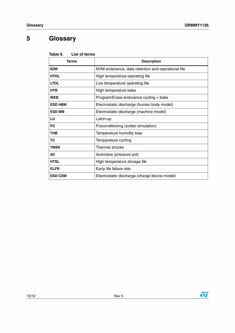
5 Glossary
Table 9. List of terms
Terms Description
EDR NVM endurance, data retention and operational life
HTOL High temperature operating life
LTOL Low temperature operating life
HTB High temperature bake
WEB Program/Erase endurance cycling + bake
ESD HBM Electrostatic discharge (human body model)
ESD MM Electrostatic discharge (machine model)
LU Latch-up
PC Preconditioning (solder simulation)
THB Temperature humidity bias
TC Temperature cycling
TMSK Thermal shocks
AC Autoclave (pressure pot)
HTSL High temperature storage life
ELFR Early life failure rate
ESD CDM Electrostatic discharge (charge device model)
QRMMY1207 Revision history
Rev 3 13/14
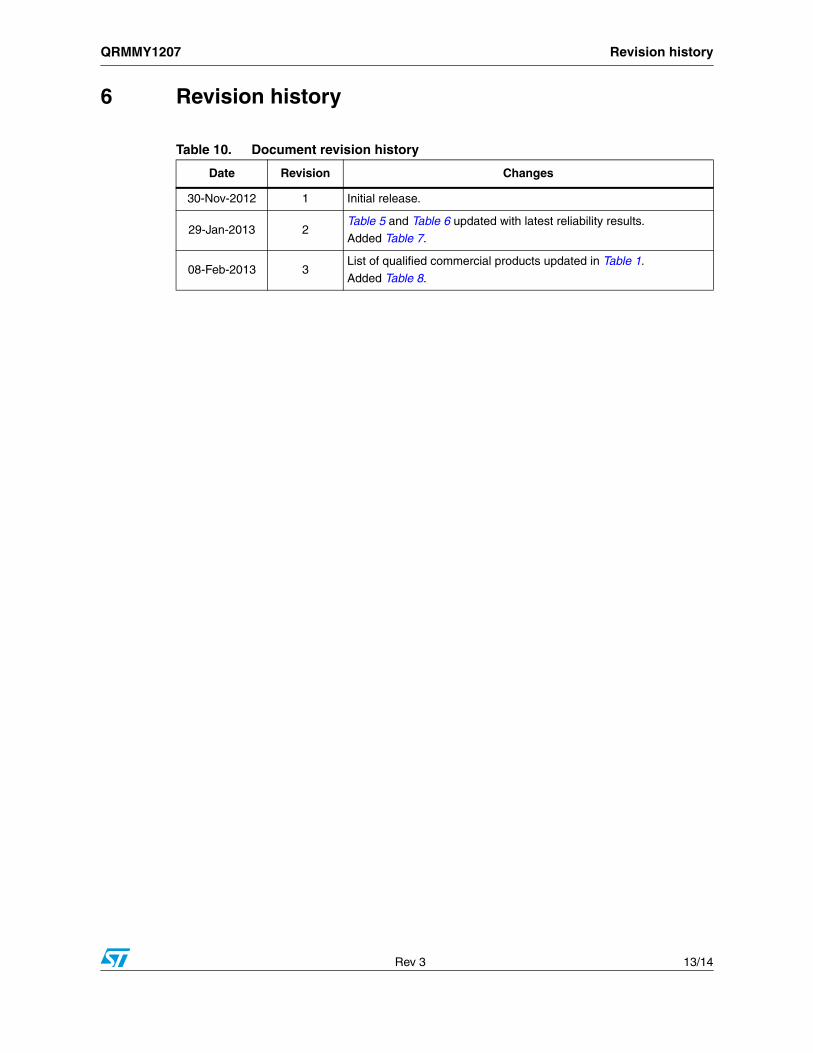
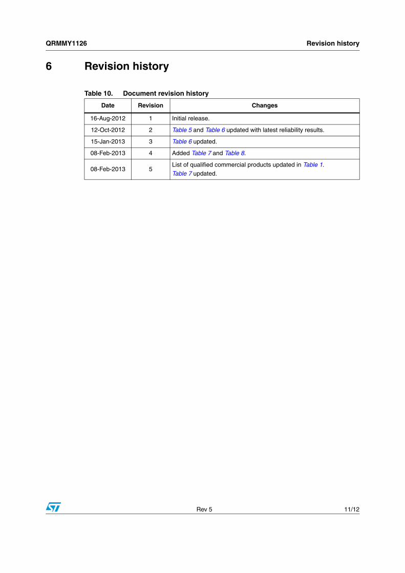
6 Revision history
Table 10. Document revision history
Date Revision Changes
30-Nov-2012 1 Initial release.
29-Jan-2013 2Table 5 and Table 6 updated with latest reliability results.
Added Table 7.
08-Feb-2013 3List of qualified commercial products updated in Table 1.
Added Table 8.
February 2013 Rev 5 1/12
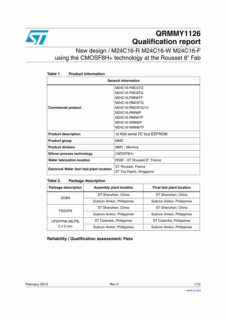
QRMMY1126Qualification report
New design / M24C16-R M24C16-W M24C16-F using the CMOSF8H+ technology at the Rousset 8” Fab
Reliability / Qualification assessment: Pass
Table 1. Product information
General information
Commercial product
M24C16-FMC5TG
M24C16-FMC6TGM24C16-FMN6TP
M24C16-RMC6TG
M24C16-RMC6TG/12M24C16-RMN6P
M24C16-RMN6TP
M24C16-WMN6PM24C16-WMN6TP
Product description 16 Kbit serial I²C bus EEPROM
Product group MMS
Product division MMY - Memory
Silicon process technology CMOSF8H+
Wafer fabrication location RS8F - ST Rousset 8”, France
Electrical Wafer Sort test plant locationST Rousset, France
ST Toa Payoh, Singapore
Table 2. Package description
Package description Assembly plant location Final test plant location
SO8NST Shenzhen, China ST Shenzhen, China
Subcon Amkor, Philippines Subcon Amkor, Philippines
TSSOP8ST Shenzhen, China ST Shenzhen, China
Subcon Amkor, Philippines Subcon Amkor, Philippines
UFDFPN8 (MLP8)
2 x 3 mm
ST Calamba, Philippines ST Calamba, Philippines
Subcon Amkor, Philippines Subcon Amkor, Philippines
www.st.com
Reliability evaluation overview QRMMY1126
2/12 Rev 5
1 Reliability evaluation overview
1.1 ObjectivesThis qualification report summarizes the results of the reliability trials that were performed to qualify the new design M24C16 using the CMOSF8H+ silicon process technology at the ST Rousset 8” diffusion fab.
The voltage and temperature ranges covered by this document are:
● 2.5 to 5.5 V at –40 to 85 °C for -W devices
● 1.8 to 5.5 V at –40 to 85 °C for -R devices
● 1.7 to 5.5 V at –40 to 85 °C for -F devices
The CMOSF8H+ is closely derived from CMOSF8H silicon process technology (already used for production of EEPROM densities ranging from 32 Kb to 2 Mb), with a more compact layout, in order to achieve a competitive die size.
This document serves for the qualification of the named product and the named silicon process technology in the named diffusion plant.
1.2 ConclusionThe new design M24C16 using the CMOSF8H+ silicon process technology at the ST Rousset 8” diffusion fab has passed all reliability requirements and all products described in Table 1 are qualified.
Qualification tests for products assembled in TSSOP8 (not yet listed in Table 1) are ongoing with positive preliminary reliability results.
Refer to Section 3: Reliability test results for details on the test results.
QRMMY1126 Device characteristics
Rev 5 3/12
2 Device characteristics
Device descriptionThe M24C16-x devices are I2C-compatible electrically erasable programmable memories (EEPROM). They are organized as 2 Kb × 8 bits.
The device behaves as a slave in the I2C protocol, with all memory operations synchronized by the serial clock. Read and Write operations are initiated by a Start condition, generated by the bus master. The Start condition is followed by a device select code and a Read/Write bit (RW) terminated by an acknowledge bit.
When writing data to the memory, the device inserts an acknowledge bit during the 9th bit time, following the bus master’s 8-bit transmission. When data is read by the bus master, the bus master acknowledges the receipt of the data byte in the same way. Data transfers are terminated by a Stop condition after an Ack for Write, and after a NoAck for Read.
Refer to the product datasheet for more details.
Reliability test results QRMMY1126
4/12 Rev 5
3 Reliability test results
This section contains a general description of the reliability evaluation strategy.
The named products are qualified using the standard STMicroelectronics corporate procedures for quality and reliability.
The product vehicle used for the die qualification is described in Table 3.
The product vehicles used for package qualification are described in Table 4.
3.1 Reliability test plan and result summaryThe reliability test plan and the result summary are presented as follows
● in Table 5 for die-oriented tests.
● in Table 6 for SO8N ST Shenzhen / subcontractor Amkor package-oriented tests.
● in Table 7 for TSSOP8 ST Shenzhen / subcontractor Amkor package-oriented tests.
● in Table 8 for UFDFPN8 (MLP8) 2 x 3 mm ST Calamba / subcontractor Amkorpackage-oriented tests.
Table 3. Product vehicle used for die qualification
ProductSilicon process
technologyWafer fabrication
locationPackage
descriptionAssembly plant
location
M24C16 CMOSF8H+ ST Rousset 8” CDIP8Engineering assy
(1)
1. CDIP8 is a engineering ceramic package used only for die-oriented reliability trials.
Table 4. Product vehicle used for package qualification
ProductSilicon process
technologyWafer fabrication
locationPackage description
Assembly plant location
M24C16 CMOSF8H+ ST Rousset 8”
SO8NST Shenzhen / Subcon Amkor
TSSOP8ST Shenzhen / Subcon Amkor
UFDFPN8 (MLP8)
2 x 3 mmST Calamba / Subcon Amkor
QRMMY1126 Reliability test results
Rev 5 5/12
Table 5. Die-oriented reliability test plan and result summary (CDIP8 / Engineering package)
Test
Test short description(1)
Method ConditionsSample size / lots
No. of
lotsDuration
Results fail / sample size
M24C16
Lot 1 Lot 2 Lot 3
EDR
High temperature operating life after endurance
AEC-Q100-0051 million E/W cycles at 25 °C then:
HTOL 150 °C, 6 V80 3
168 hrs 0/80 0/80 0/80
504 hrs 0/80 0/80 0/80
1008 hrs 0/80 0/80 0/80
Data retention after endurance
AEC-Q100-0051 million E/W cycles at 25 °C then:
HTSL at 150 °C80 3
168 hrs 0/80 0/80 0/80
504 hrs 0/80 0/80 0/80
1008 hrs 0/80 0/80 0/80
LTOL
Low temperature operating life
JESD22-A108 –40 °C, 6 V 80 3
168 hrs 0/80 0/80 0/80
504 hrs 0/80 0/80 0/80
1008 hrs 0/80 0/80 0/80
HTSL
High temperature storage life
JESD22-A103 Retention bake at 200 °C 80 3
168 hrs 0/80 0/80 0/80
504 hrs 0/80 0/80 0/80
1008 hrs 0/80 0/80 0/80
WEB
Program/erase endurance cycling + bake
Internal spec.1 Million E/W cycles at 25 °C then:
Retention bake at 200 °C / 48 hours
80 31 Million cycles /48 hrs
0/80 (2) 0/80 (2) 0/80 (2)
ESD HBM
Electrostatic discharge (human body model)
AEC-Q100-002JESD22-A114
C = 100 pF, R= 1500 Ω 27 3 N/APass
3000 VPass
3000 VPass
3000 V
ESD MM
Electrostatic discharge (machine model)
AEC-Q100-003JESD22-A115
C = 200 pF, R = 0 Ω 12 3 N/APass400 V
Pass400 V
Pass400 V
LU
Latch-up (current injection and overvoltage stress)
AEC-Q100-004JESD78A
At maximum operating temperature (150 °C)
6 3 N/AClass II -Level A
Class II -Level A
Class II -Level A
1. See Table 9: List of terms for a definition of abbreviations.
2. First rejects after 10 million cycles + bake.
Reliability test results QRMMY1126
6/12 Rev 5
Table 6. Package-oriented reliability test plan and result summary (SO8N / ST Shenzhen & subcontractor Amkor)
Test
Test short description(1)
Method ConditionsSample size / lots
No. of
lotsDuration
Results fail / sample size
M24C16
Lot 1 Lot 2 Lot 3
PC
Preconditioning: moisture sensitivity level 1
JESD22-A113J-STD-020D
MSL1, peak temperature at 260 °C, 3 IReflow
1145 3 N/A 0/1145 0/1145 0/1145
THB(2)
Temperature humidity bias
AEC-Q100-JESD22-A101
85 °C, 85% RH, bias 5.5 V 80 31008 hrs 0/80 0/80 0/80
2008 hrs 0/80 0/80 0/80
TC (2)
Temperature cycling
AEC-Q100-JESD22-A104
–65 °C / +150 °C 80 31000
cycles0/80 0/80 0/80
TMSK(2)
Thermal shocks
JESD22-A106 –55 °C / +125 °C 25 3200
shocks0/25 0/25 0/25
AC (2)
Autoclave (pressure pot)
AEC-Q100-JESD22-A102
121 °C, 100% RH at 2 ATM 80 3 168 hrs 0/80 0/80 0/80
HTSL(2)
High temperature storage life
AEC-Q100-JESD22-A103
Retention bake at 150 °C 80 31008 hrs 0/80 0/80 0/80
2008 hrs 0/80 0/80 0/80
ELFR(2)
Early life failure rate
AEC-Q100-008
HTOL at 150 °C, 6V 800 3 48 hrs 0/800 0/800 0/800
ESD CDM
Electrostatic discharge (charge device model)
AEC-Q100-011
JESD22-C101
Field induced charging method
18 1 N/APASS
> 1500V- -
1. See Table 9: List of terms for a definition of abbreviations.
2. THB-, TC-, TMSK-, AC-, HTSL and ELFR- dedicated parts are first subject to preconditioning flow.
QRMMY1126 Reliability test results
Rev 5 7/12
Table 7. Package-oriented reliability test plan and result summary (TSSOP8 / ST Shenzhen & subcontractor Amkor)
Test
Test short description(1)
Method ConditionsSample size / lots
No. of
lotsDuration
Results fail / sample size
M24C16
Lot 1 Lot 2 Lot 3
PC
Preconditioning: moisture sensitivity level 1
JESD22-A113J-STD-020D
MSL1, peak temperature at 260 °C, 3 IReflow
1145 3 N/A 0/1145 0/1145 0/1145
THB(2)
Temperature humidity bias
AEC-Q100-JESD22-A101
85 °C, 85% RH, bias 5.5 V 80 3
168 hrs 0/80 0/80 0/80
504 hrs 0/80 0/80Results FC W07
1008 hrsResults FC W10
Results FC W10
Results FC W11
TC (2)
Temperature cycling
AEC-Q100-JESD22-A104
–65 °C / +150 °C 80 3
500 cycles
0/80 0/80 0/80
1000 cycles
0/80 0/80Results FC W07
TMSK(2)
Thermal shocks
JESD22-A106 –55 °C / +125 °C 25 3200
shocks0/25 0/25 0/25
AC (2)
Autoclave (pressure pot)
AEC-Q100-JESD22-A102
121 °C, 100% RH at 2 ATM 80 3 168 hrs 0/80 0/80 0/80
HTSL(2)
High temperature storage life
AEC-Q100-JESD22-A103
Retention bake at 150 °C 80 3
168 hrs 0/80 0/80 0/80
504 hrs 0/80 0/80Results FC W07
1008 hrsResults FC W10
Results FC W10
Results FC W11
ELFR(2)
Early life failure rate
AEC-Q100-008
HTOL at 150 °C, 6V 800 3 48 hrs 0/800 0/800Results FC W08
ESD CDM
Electrostatic discharge (charge device model)
AEC-Q100-011
JESD22-C101
Field induced charging method
18 1 N/APASS
> 1500V- -
1. See Table 9: List of terms for a definition of abbreviations.
2. THB-, TC-, TMSK-, AC-, HTSL and ELFR- dedicated parts are first subject to preconditioning flow.
Reliability test results QRMMY1126
8/12 Rev 5
Table 8. Package-oriented reliability test plan and result summary (UFDFPN8 MLP8 2 x 3 mm / ST Calamba & subcontractor Amkor)
Test
Test short description(1)
Method ConditionsSample size / lots
No. of
lotsDuration
Results fail / sample size
M24C16
Lot 1 Lot 2 Lot 3
PC
Preconditioning: moisture sensitivity level 1
JESD22-A113J-STD-020D
MSL1, peak temperature at 260 °C, 3 IReflow
345 1 N/A 0/345 0/345 0/345
THB(2)
Temperature humidity bias
AEC-Q100-JESD22-A101
85 °C, 85% RH, bias 5.5 V
80 1 1008 hrs 0/80 0/80 0/80
TC (2)
Temperature cycling
AEC-Q100-JESD22-A104
–65 °C / +150 °C 80 11000 cycles
0/80 0/80 0/80
TMSK(2)
Thermal shocks
JESD22-A106 –55 °C / +125 °C 25 1200
shocks0/25 0/25 0/25
AC (2)
Autoclave (pressure pot)
AEC-Q100-JESD22-A102
121 °C, 100% RH
at 2 ATM80 1 168 hrs 0/80 0/80 0/80
HTSL(2)
High temperature storage life
AEC-Q100-JESD22-A103
Retention bake at 150 °C 80 1 1008 hrs 0/80 0/80 0/80
ESD CDM
Electrostatic discharge (charge device model)
AEC-Q100-011
JESD22-C101Field induced charging method 18 1 N/A
PASS > 1500V
- -
1. See Table 9: List of terms for a definition of abbreviations.
2. THB-, TC-, TMSK-, AC- and HTSL- dedicated parts are first subject to preconditioning flow.
QRMMY1126 Applicable and reference documents
Rev 5 9/12
4 Applicable and reference documents
● AEC-Q100: Stress test qualification for integrated circuits
● SOP 2.6.10: General product qualification procedure
● SOP 2.6.11: Program management for product qualification
● SOP 2.6.12: Design criteria for product qualification
● SOP 2.6.14: Reliability requirements for product qualification
● SOP 2.6.19: Process maturity level
● SOP 2.6.2: Process qualification and transfer management
● SOP 2.6.20: New process / New product qualification
● SOP 2.6.7: Product maturity level
● SOP 2.6.9: Package and process maturity management in Back End
● SOP 2.7.5: Automotive products definition and status
● JESD22-A101: Steady state temperature humidity bias life test
● JESD22-A102: Accelerated moisture resistance - unbiased autoclave
● JESD22-A103: High temperature storage life
● JESD22-A104: Temperature cycling
● JESD22-A106: Thermal shock
● JESD22-A108: Temperature, bias, and operating life
● JESD22-A113: Preconditioning of nonhermetic surface mount devices prior to reliabilitytesting
● JESD22-A114: Electrostatic discharge (ESD) sensitivity testing human body model(HBM)
● JESD22-A115: Electrostatic discharge (ESD) sensitivity testing machine model (MM)
● JESD78: IC Latch-up test
● J-STD-020D: Moisture/reflow sensitivity classification for nonhermetic solid statesurface mount devices
Glossary QRMMY1126
10/12 Rev 5
5 Glossary
Table 9. List of terms
Terms Description
EDR NVM endurance, data retention and operational life
HTOL High temperature operating life
LTOL Low temperature operating life
HTB High temperature bake
WEB Program/Erase endurance cycling + bake
ESD HBM Electrostatic discharge (human body model)
ESD MM Electrostatic discharge (machine model)
LU Latch-up
PC Preconditioning (solder simulation)
THB Temperature humidity bias
TC Temperature cycling
TMSK Thermal shocks
AC Autoclave (pressure pot)
HTSL High temperature storage life
ELFR Early life failure rate
ESD CDM Electrostatic discharge (charge device model)
QRMMY1126 Revision history
Rev 5 11/12
6 Revision history
Table 10. Document revision history
Date Revision Changes
16-Aug-2012 1 Initial release.
12-Oct-2012 2 Table 5 and Table 6 updated with latest reliability results.
15-Jan-2013 3 Table 6 updated.
08-Feb-2013 4 Added Table 7 and Table 8.
08-Feb-2013 5List of qualified commercial products updated in Table 1.Table 7 updated.
8
M24C01, M24C02, M24C04, M24C16, 1-, 2-, 4-, 16-Kbit I²C Bus EEPROM Industrial grade / UFDFPN8 & TSSOP8 packages
Redesign and upgrade to the CMOSF8H+ process technology
Document Revision History
Date Rev. Description of the Revision January 18, 2013 1.00 First draft creation
Source Documen ts & Reference Documents
Source document Title Rev.: Date:
April 2011 Doc ID 5067 Rev 17 1/38
1
M24C16-x M24C08-xM24C04-x M24C02-x M24C01-x
16 Kbit, 8 Kbit, 4 Kbit, 2 Kbit and 1 Kbit serial I²C bus EEPROM
Features■ Supports both the 100 kHz I2C Standard-mode
and the 400 kHz I2C Fast-mode
■ Single supply voltage:– 2.5 V to 5.5 V for M24Cxx-W– 1.8 V to 5.5 V for M24Cxx– 1.7 V to 5.5 V for M24Cxx-F
■ Write Control input
■ Byte and Page Write (up to 16 bytes)
■ Random and Sequential Read modes
■ Self-timed programming cycle
■ Automatic address incrementing
■ Enhanced ESD/latch-up protection
■ More than 1 million write cycles
■ More than 40-year data retention
■ Packages:– SO8, TSSOP8, UFDFPN8: ECOPACK2®
(RoHS-compliant and Halogen-free)– PDIP8: ECOPACK1® (RoHS-compliant)
1. Only M24C08-F and M24C16-F devices are offered inthe WLCSP package.
2. Only M24C08-F devices are offered in the ThinWLCSP package.
Table 1. Device summary
Reference Part number
M24C16-x
M24C16-W
M24C16-R
M24C16-F
M24C08-x
M24C08-W
M24C08-R
M24C08-F
M24C04-x
M24C04-W
M24C04-R
M24C04-F
M24C02-xM24C02-W
M24C02-R
M24C01-xM24C01-W
M24C01-R
PDIP8 (BN)
SO8 (MN)150 mils width
TSSOP8 (DW)169 mils width
UFDFPN8 (MB, MC)2 × 3 mm (MLP)
WLCSP (CS)(1)
Thin WLCSP (CT)(2)
www.st.com
Contents M24C16, M24C08, M24C04, M24C02, M24C01
2/38 Doc ID 5067 Rev 17
Contents
1 Description . . . . . . . . . . . . . . . . . . . . . . . . . . . . . . . . . . . . . . . . . . . . . . . . . 6
2 Signal description . . . . . . . . . . . . . . . . . . . . . . . . . . . . . . . . . . . . . . . . . . . 8
2.1 Serial Clock (SCL) . . . . . . . . . . . . . . . . . . . . . . . . . . . . . . . . . . . . . . . . . . . 8
2.2 Serial Data (SDA) . . . . . . . . . . . . . . . . . . . . . . . . . . . . . . . . . . . . . . . . . . . . 8
2.3 Chip Enable (E0, E1, E2) . . . . . . . . . . . . . . . . . . . . . . . . . . . . . . . . . . . . . . 8
2.3.1 Write Control (WC) . . . . . . . . . . . . . . . . . . . . . . . . . . . . . . . . . . . . . . . . . 8
2.4 Supply voltage (VCC) . . . . . . . . . . . . . . . . . . . . . . . . . . . . . . . . . . . . . . . . . 9
2.4.1 Operating supply voltage VCC . . . . . . . . . . . . . . . . . . . . . . . . . . . . . . . . . . . . . . . . . . 9
2.4.2 Power-up conditions . . . . . . . . . . . . . . . . . . . . . . . . . . . . . . . . . . . . . . . . 9
2.4.3 Device reset . . . . . . . . . . . . . . . . . . . . . . . . . . . . . . . . . . . . . . . . . . . . . . . 9
2.4.4 Power-down conditions . . . . . . . . . . . . . . . . . . . . . . . . . . . . . . . . . . . . . . 9
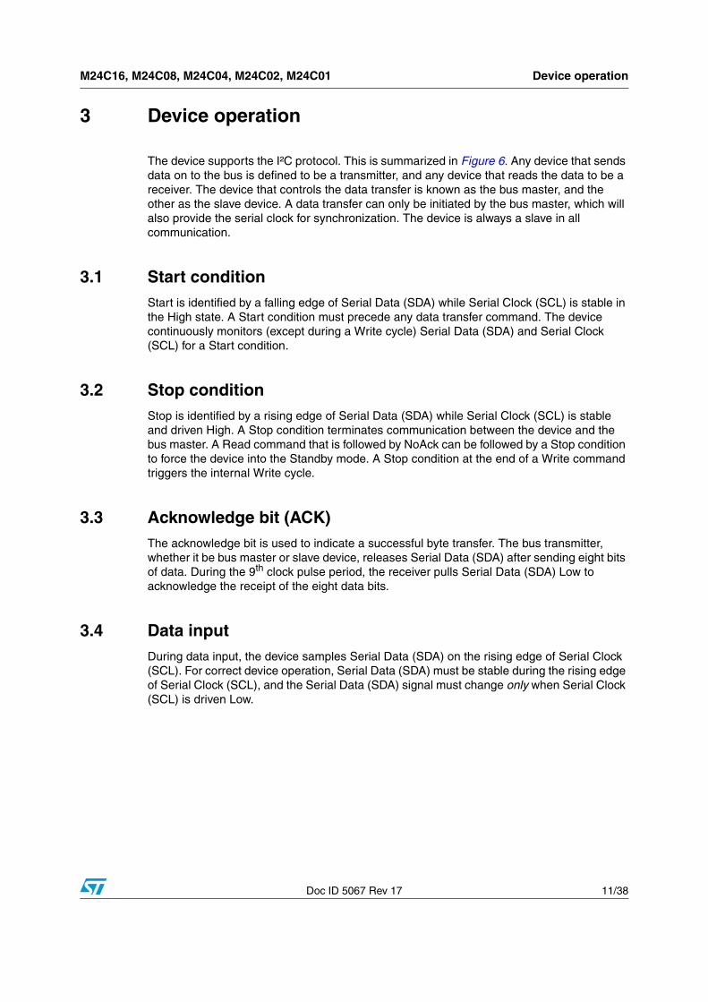
3 Device operation . . . . . . . . . . . . . . . . . . . . . . . . . . . . . . . . . . . . . . . . . . . 11
3.1 Start condition . . . . . . . . . . . . . . . . . . . . . . . . . . . . . . . . . . . . . . . . . . . . . 11
3.2 Stop condition . . . . . . . . . . . . . . . . . . . . . . . . . . . . . . . . . . . . . . . . . . . . . 11
3.3 Acknowledge bit (ACK) . . . . . . . . . . . . . . . . . . . . . . . . . . . . . . . . . . . . . . . 11
3.4 Data input . . . . . . . . . . . . . . . . . . . . . . . . . . . . . . . . . . . . . . . . . . . . . . . . . 11
3.5 Memory addressing . . . . . . . . . . . . . . . . . . . . . . . . . . . . . . . . . . . . . . . . . 12
3.6 Write operations . . . . . . . . . . . . . . . . . . . . . . . . . . . . . . . . . . . . . . . . . . . . 13
3.6.1 Byte Write . . . . . . . . . . . . . . . . . . . . . . . . . . . . . . . . . . . . . . . . . . . . . . . 14
3.6.2 Page Write . . . . . . . . . . . . . . . . . . . . . . . . . . . . . . . . . . . . . . . . . . . . . . . 14
3.6.3 Minimizing system delays by polling on ACK . . . . . . . . . . . . . . . . . . . . . 16
3.7 Read operations . . . . . . . . . . . . . . . . . . . . . . . . . . . . . . . . . . . . . . . . . . . . 17
3.7.1 Random Address Read . . . . . . . . . . . . . . . . . . . . . . . . . . . . . . . . . . . . . 17
3.7.2 Current Address Read . . . . . . . . . . . . . . . . . . . . . . . . . . . . . . . . . . . . . . 18
3.7.3 Sequential Read . . . . . . . . . . . . . . . . . . . . . . . . . . . . . . . . . . . . . . . . . . 18
3.7.4 Acknowledge in Read mode . . . . . . . . . . . . . . . . . . . . . . . . . . . . . . . . . 18
4 Initial delivery state . . . . . . . . . . . . . . . . . . . . . . . . . . . . . . . . . . . . . . . . . 19
5 Maximum rating . . . . . . . . . . . . . . . . . . . . . . . . . . . . . . . . . . . . . . . . . . . . 19
6 DC and AC parameters . . . . . . . . . . . . . . . . . . . . . . . . . . . . . . . . . . . . . . 20
M24C16, M24C08, M24C04, M24C02, M24C01 Contents
Doc ID 5067 Rev 17 3/38
7 Package mechanical data . . . . . . . . . . . . . . . . . . . . . . . . . . . . . . . . . . . . 27
8 Part numbering . . . . . . . . . . . . . . . . . . . . . . . . . . . . . . . . . . . . . . . . . . . . 33
9 Revision history . . . . . . . . . . . . . . . . . . . . . . . . . . . . . . . . . . . . . . . . . . . 34
List of tables M24C16, M24C08, M24C04, M24C02, M24C01
4/38 Doc ID 5067 Rev 17
List of tables
Table 1. Device summary . . . . . . . . . . . . . . . . . . . . . . . . . . . . . . . . . . . . . . . . . . . . . . . . . . . . . . . . . . 1Table 2. Signal names . . . . . . . . . . . . . . . . . . . . . . . . . . . . . . . . . . . . . . . . . . . . . . . . . . . . . . . . . . . . 6Table 3. Device select code . . . . . . . . . . . . . . . . . . . . . . . . . . . . . . . . . . . . . . . . . . . . . . . . . . . . . . . 10Table 4. Operating modes . . . . . . . . . . . . . . . . . . . . . . . . . . . . . . . . . . . . . . . . . . . . . . . . . . . . . . . . 12Table 5. Absolute maximum ratings . . . . . . . . . . . . . . . . . . . . . . . . . . . . . . . . . . . . . . . . . . . . . . . . . 19Table 6. Operating conditions (M24Cxx-W) . . . . . . . . . . . . . . . . . . . . . . . . . . . . . . . . . . . . . . . . . . . 20Table 7. Operating conditions (M24Cxx-R) . . . . . . . . . . . . . . . . . . . . . . . . . . . . . . . . . . . . . . . . . . . 20Table 8. Operating conditions (M24Cxx-F) . . . . . . . . . . . . . . . . . . . . . . . . . . . . . . . . . . . . . . . . . . . . 20Table 9. DC characteristics (M24Cxx-W, device grade 6) . . . . . . . . . . . . . . . . . . . . . . . . . . . . . . . . 21Table 10. DC characteristics (M24Cxx-W, device grade 3) . . . . . . . . . . . . . . . . . . . . . . . . . . . . . . . . 21Table 11. DC characteristics (M24Cxx-R) . . . . . . . . . . . . . . . . . . . . . . . . . . . . . . . . . . . . . . . . . . . . . 22Table 12. DC characteristics (M24Cxx-F). . . . . . . . . . . . . . . . . . . . . . . . . . . . . . . . . . . . . . . . . . . . . . 23Table 13. AC measurement conditions. . . . . . . . . . . . . . . . . . . . . . . . . . . . . . . . . . . . . . . . . . . . . . . . 23Table 14. Input parameters. . . . . . . . . . . . . . . . . . . . . . . . . . . . . . . . . . . . . . . . . . . . . . . . . . . . . . . . . 23Table 15. AC characteristics at 400 kHz (I2C Fast-mode) (M24Cxx-W, M24Cxx-R,
M24Cxx-F) . . . . . . . . . . . . . . . . . . . . . . . . . . . . . . . . . . . . . . . . . . . . . . . . . . . . . . . . . . . . . 24Table 16. AC characteristics at 100 kHz (I2C Standard-mode) (M24Cxx-W,
M24Cxx-R, M24Cxx-F) . . . . . . . . . . . . . . . . . . . . . . . . . . . . . . . . . . . . . . . . . . . . . . . . . . . . 25Table 17. M24C08: WLCSP (0.5 mm height) 0.4 mm pitch, 5 bumps, package data . . . . . . . . . . . . 27Table 18. M24C08: Thin WLCSP (0.3 mm height), 0.4 mm pitch, 5 bumps, package data . . . . . . . . 28Table 19. M24C16: WLCSP (0.5 mm height) 0.4 mm pitch, 5 bumps, package data . . . . . . . . . . . . 28Table 20. SO8 narrow – 8 lead plastic small outline, 150 mils body width,
package mechanical data . . . . . . . . . . . . . . . . . . . . . . . . . . . . . . . . . . . . . . . . . . . . . . . . . . 29Table 21. UFDFPN8 (MLP8) 8-lead ultra thin fine pitch dual flat package no lead
2 x 3 mm, data . . . . . . . . . . . . . . . . . . . . . . . . . . . . . . . . . . . . . . . . . . . . . . . . . . . . . . . . . . 30Table 22. TSSOP8 – 8 lead thin shrink small outline, package mechanical data. . . . . . . . . . . . . . . . 31Table 23. PDIP8 – 8 pin plastic DIP, 0.25 mm lead frame, package mechanical data. . . . . . . . . . . . 32Table 24. Ordering information scheme . . . . . . . . . . . . . . . . . . . . . . . . . . . . . . . . . . . . . . . . . . . . . . . 33Table 25. Document revision history . . . . . . . . . . . . . . . . . . . . . . . . . . . . . . . . . . . . . . . . . . . . . . . . . 34
M24C16, M24C08, M24C04, M24C02, M24C01 List of figures
Doc ID 5067 Rev 17 5/38
List of figures
Figure 1. Logic diagram . . . . . . . . . . . . . . . . . . . . . . . . . . . . . . . . . . . . . . . . . . . . . . . . . . . . . . . . . . . . 6Figure 2. 8-pin package connections (top view) . . . . . . . . . . . . . . . . . . . . . . . . . . . . . . . . . . . . . . . . . 7Figure 3. WLCSP and thin WLCSP connections
(top view, marking side, with balls on the underside) . . . . . . . . . . . . . . . . . . . . . . . . . . . . . 7Figure 4. Device select code . . . . . . . . . . . . . . . . . . . . . . . . . . . . . . . . . . . . . . . . . . . . . . . . . . . . . . . . 8Figure 5. Maximum RP value versus bus parasitic capacitance (C) for an I²C bus . . . . . . . . . . . . . . 9Figure 6. I²C bus protocol . . . . . . . . . . . . . . . . . . . . . . . . . . . . . . . . . . . . . . . . . . . . . . . . . . . . . . . . . 10Figure 7. Write mode sequences with WC = 1 (data write inhibited) . . . . . . . . . . . . . . . . . . . . . . . . . 13Figure 8. Write mode sequences with WC = 0 (data write enabled) . . . . . . . . . . . . . . . . . . . . . . . . . 15Figure 9. Write cycle polling flowchart using ACK . . . . . . . . . . . . . . . . . . . . . . . . . . . . . . . . . . . . . . . 16Figure 10. Read mode sequences. . . . . . . . . . . . . . . . . . . . . . . . . . . . . . . . . . . . . . . . . . . . . . . . . . . . 17Figure 11. AC measurement I/O waveform . . . . . . . . . . . . . . . . . . . . . . . . . . . . . . . . . . . . . . . . . . . . . 23Figure 12. AC waveforms . . . . . . . . . . . . . . . . . . . . . . . . . . . . . . . . . . . . . . . . . . . . . . . . . . . . . . . . . . 26Figure 13. WLCSP (0.5 mm) and Thin WLCSP (0.3 mm) 0.4 mm pitch 5 bumps,
package outline . . . . . . . . . . . . . . . . . . . . . . . . . . . . . . . . . . . . . . . . . . . . . . . . . . . . . . . . . 27Figure 14. SO8 narrow – 8 lead plastic small outline, 150 mils body width, package outline . . . . . . . 29Figure 15. UFDFPN8 (MLP8) 8-lead ultra thin fine pitch dual flat package no lead
2 x 3 mm, outline . . . . . . . . . . . . . . . . . . . . . . . . . . . . . . . . . . . . . . . . . . . . . . . . . . . . . . . . 30Figure 16. TSSOP8 – 8 lead thin shrink small outline, package outline . . . . . . . . . . . . . . . . . . . . . . . 31Figure 17. PDIP8 – 8 pin plastic DIP, 0.25 mm lead frame, package outline . . . . . . . . . . . . . . . . . . . 32
Description M24C16, M24C08, M24C04, M24C02, M24C01
6/38 Doc ID 5067 Rev 17
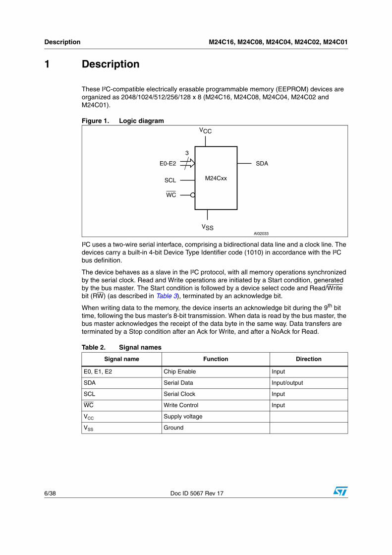
1 Description
These I²C-compatible electrically erasable programmable memory (EEPROM) devices are organized as 2048/1024/512/256/128 x 8 (M24C16, M24C08, M24C04, M24C02 and M24C01).
Figure 1. Logic diagram
I²C uses a two-wire serial interface, comprising a bidirectional data line and a clock line. The devices carry a built-in 4-bit Device Type Identifier code (1010) in accordance with the I²C bus definition.
The device behaves as a slave in the I²C protocol, with all memory operations synchronized by the serial clock. Read and Write operations are initiated by a Start condition, generated by the bus master. The Start condition is followed by a device select code and Read/Write bit (RW) (as described in Table 3), terminated by an acknowledge bit.
When writing data to the memory, the device inserts an acknowledge bit during the 9th bit time, following the bus master’s 8-bit transmission. When data is read by the bus master, the bus master acknowledges the receipt of the data byte in the same way. Data transfers are terminated by a Stop condition after an Ack for Write, and after a NoAck for Read.
Table 2. Signal names
Signal name Function Direction
E0, E1, E2 Chip Enable Input
SDA Serial Data Input/output
SCL Serial Clock Input
WC Write Control Input
VCC Supply voltage
VSS Ground
AI02033
3
E0-E2 SDA
VCC
M24Cxx
WC
SCL
VSS
M24C16, M24C08, M24C04, M24C02, M24C01 Description
Doc ID 5067 Rev 17 7/38
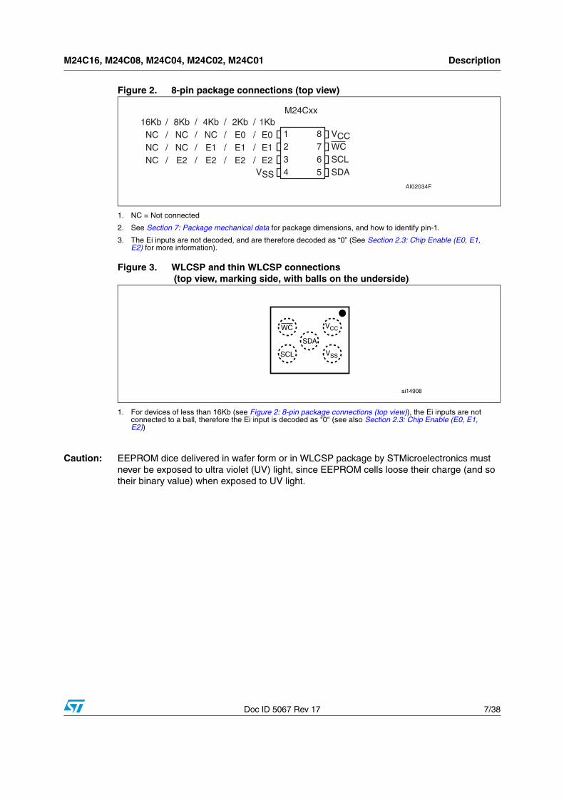
Figure 2. 8-pin package connections (top view)
1. NC = Not connected
2. See Section 7: Package mechanical data for package dimensions, and how to identify pin-1.
3. The Ei inputs are not decoded, and are therefore decoded as “0” (See Section 2.3: Chip Enable (E0, E1,E2) for more information).
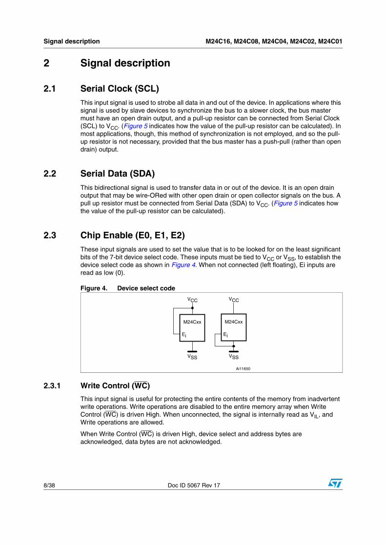
Figure 3. WLCSP and thin WLCSP connections (top view, marking side, with balls on the underside)
1. For devices of less than 16Kb (see Figure 2: 8-pin package connections (top view)), the Ei inputs are notconnected to a ball, therefore the Ei input is decoded as "0" (see also Section 2.3: Chip Enable (E0, E1,E2))
Caution: EEPROM dice delivered in wafer form or in WLCSP package by STMicroelectronics must never be exposed to ultra violet (UV) light, since EEPROM cells loose their charge (and so their binary value) when exposed to UV light.
SDAVSS
SCLWCVCC
AI02034F
M24Cxx
1234
8765
16Kb / 8Kb / 4Kb / 2Kb / 1Kb NC / NC / NC / E0 / E0 NC / NC / E1 / E1 / E1 NC / E2 / E2 / E2 / E2
VCCWC
SDA
SCL VSS
ai14908
Signal description M24C16, M24C08, M24C04, M24C02, M24C01
8/38 Doc ID 5067 Rev 17
2 Signal description
2.1 Serial Clock (SCL)This input signal is used to strobe all data in and out of the device. In applications where this signal is used by slave devices to synchronize the bus to a slower clock, the bus master must have an open drain output, and a pull-up resistor can be connected from Serial Clock (SCL) to VCC. (Figure 5 indicates how the value of the pull-up resistor can be calculated). In most applications, though, this method of synchronization is not employed, and so the pull-up resistor is not necessary, provided that the bus master has a push-pull (rather than open drain) output.
2.2 Serial Data (SDA)This bidirectional signal is used to transfer data in or out of the device. It is an open drain output that may be wire-ORed with other open drain or open collector signals on the bus. A pull up resistor must be connected from Serial Data (SDA) to VCC. (Figure 5 indicates how the value of the pull-up resistor can be calculated).
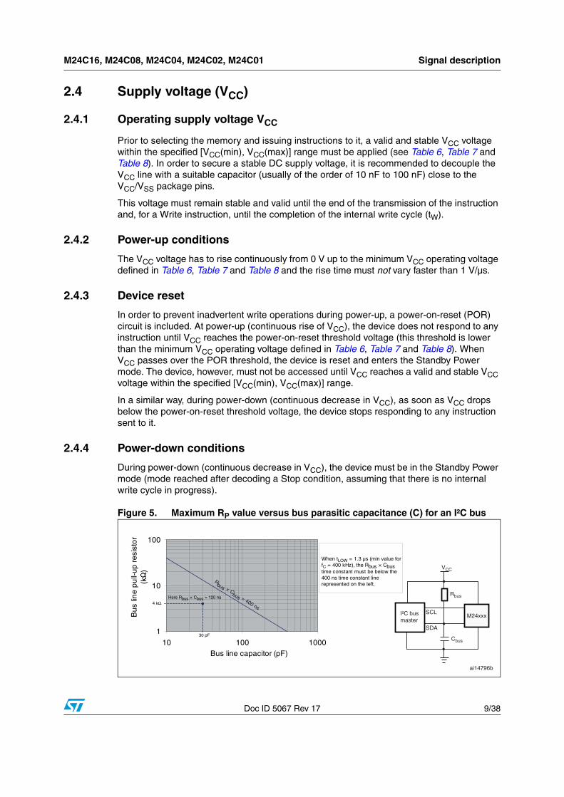
2.3 Chip Enable (E0, E1, E2)These input signals are used to set the value that is to be looked for on the least significant bits of the 7-bit device select code. These inputs must be tied to VCC or VSS, to establish the device select code as shown in Figure 4. When not connected (left floating), Ei inputs are read as low (0).
Figure 4. Device select code
2.3.1 Write Control (WC)
This input signal is useful for protecting the entire contents of the memory from inadvertent write operations. Write operations are disabled to the entire memory array when Write Control (WC) is driven High. When unconnected, the signal is internally read as VIL, and Write operations are allowed.
When Write Control (WC) is driven High, device select and address bytes are acknowledged, data bytes are not acknowledged.
Ai11650
VCC
M24Cxx
VSS
Ei
VCC
M24Cxx
VSS
Ei
M24C16, M24C08, M24C04, M24C02, M24C01 Signal description
Doc ID 5067 Rev 17 9/38
2.4 Supply voltage (VCC)
2.4.1 Operating supply voltage VCC
Prior to selecting the memory and issuing instructions to it, a valid and stable VCC voltage within the specified [VCC(min), VCC(max)] range must be applied (see Table 6, Table 7 and Table 8). In order to secure a stable DC supply voltage, it is recommended to decouple the VCC line with a suitable capacitor (usually of the order of 10 nF to 100 nF) close to the VCC/VSS package pins.
This voltage must remain stable and valid until the end of the transmission of the instruction and, for a Write instruction, until the completion of the internal write cycle (tW).
2.4.2 Power-up conditions
The VCC voltage has to rise continuously from 0 V up to the minimum VCC operating voltage defined in Table 6, Table 7 and Table 8 and the rise time must not vary faster than 1 V/µs.
2.4.3 Device reset
In order to prevent inadvertent write operations during power-up, a power-on-reset (POR) circuit is included. At power-up (continuous rise of VCC), the device does not respond to any instruction until VCC reaches the power-on-reset threshold voltage (this threshold is lower than the minimum VCC operating voltage defined in Table 6, Table 7 and Table 8). When VCC passes over the POR threshold, the device is reset and enters the Standby Power mode. The device, however, must not be accessed until VCC reaches a valid and stable VCC voltage within the specified [VCC(min), VCC(max)] range.
In a similar way, during power-down (continuous decrease in VCC), as soon as VCC drops below the power-on-reset threshold voltage, the device stops responding to any instruction sent to it.
2.4.4 Power-down conditions
During power-down (continuous decrease in VCC), the device must be in the Standby Power mode (mode reached after decoding a Stop condition, assuming that there is no internal write cycle in progress).
Figure 5. Maximum RP value versus bus parasitic capacitance (C) for an I²C bus
1
10
100
10 100 1000Bus line capacitor (pF)
Bu
s lin
e p
ull-
up
re
sist
or
(k)
When tLOW = 1.3 µs (min value forfC = 400 kHz), the Rbus × Cbustime constant must be below the 400 ns time constant linerepresented on the left.
I²C busmaster
M24xxx
Rbus
VCC
Cbus
SCL
SDA
ai14796b
Rbus × C
bus = 400 ns
Here Rbus × Cbus = 120 ns4 kΩ
30 pF
Signal description M24C16, M24C08, M24C04, M24C02, M24C01
10/38 Doc ID 5067 Rev 17
Figure 6. I²C bus protocol
Table 3. Device select code
Device type identifier(1)
1. The most significant bit, b7, is sent first.
Chip Enable(2),(3)
2. E0, E1 and E2 are compared against the respective external pins on the memory device.
3. A10, A9 and A8 represent most significant bits of the address.
RW
b7 b6 b5 b4 b3 b2 b1 b0
M24C01 select code 1 0 1 0 E2 E1 E0 RW
M24C02 select code 1 0 1 0 E2 E1 E0 RW
M24C04 select code 1 0 1 0 E2 E1 A8 RW
M24C08 select code 1 0 1 0 E2 A9 A8 RW
M24C16 select code 1 0 1 0 A10 A9 A8 RW
SCL
SDA
SCL
SDA
SDA
Startcondition
SDAInput
SDAChange
AI00792c
Stopcondition
1 2 3 7 8 9
MSB ACK
Startcondition
SCL 1 2 3 7 8 9
MSB ACK
Stopcondition
M24C16, M24C08, M24C04, M24C02, M24C01 Device operation
Doc ID 5067 Rev 17 11/38
3 Device operation
The device supports the I²C protocol. This is summarized in Figure 6. Any device that sends data on to the bus is defined to be a transmitter, and any device that reads the data to be a receiver. The device that controls the data transfer is known as the bus master, and the other as the slave device. A data transfer can only be initiated by the bus master, which will also provide the serial clock for synchronization. The device is always a slave in all communication.
3.1 Start conditionStart is identified by a falling edge of Serial Data (SDA) while Serial Clock (SCL) is stable in the High state. A Start condition must precede any data transfer command. The device continuously monitors (except during a Write cycle) Serial Data (SDA) and Serial Clock (SCL) for a Start condition.
3.2 Stop conditionStop is identified by a rising edge of Serial Data (SDA) while Serial Clock (SCL) is stable and driven High. A Stop condition terminates communication between the device and the bus master. A Read command that is followed by NoAck can be followed by a Stop condition to force the device into the Standby mode. A Stop condition at the end of a Write command triggers the internal Write cycle.
3.3 Acknowledge bit (ACK)The acknowledge bit is used to indicate a successful byte transfer. The bus transmitter, whether it be bus master or slave device, releases Serial Data (SDA) after sending eight bits of data. During the 9th clock pulse period, the receiver pulls Serial Data (SDA) Low to acknowledge the receipt of the eight data bits.
3.4 Data inputDuring data input, the device samples Serial Data (SDA) on the rising edge of Serial Clock (SCL). For correct device operation, Serial Data (SDA) must be stable during the rising edge of Serial Clock (SCL), and the Serial Data (SDA) signal must change only when Serial Clock (SCL) is driven Low.
Device operation M24C16, M24C08, M24C04, M24C02, M24C01
12/38 Doc ID 5067 Rev 17
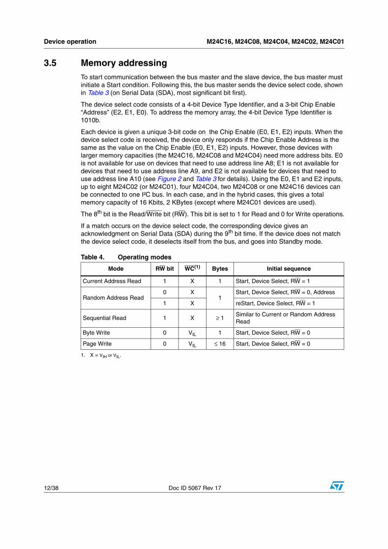
3.5 Memory addressingTo start communication between the bus master and the slave device, the bus master must initiate a Start condition. Following this, the bus master sends the device select code, shown in Table 3 (on Serial Data (SDA), most significant bit first).
The device select code consists of a 4-bit Device Type Identifier, and a 3-bit Chip Enable “Address” (E2, E1, E0). To address the memory array, the 4-bit Device Type Identifier is 1010b.
Each device is given a unique 3-bit code on the Chip Enable (E0, E1, E2) inputs. When the device select code is received, the device only responds if the Chip Enable Address is the same as the value on the Chip Enable (E0, E1, E2) inputs. However, those devices with larger memory capacities (the M24C16, M24C08 and M24C04) need more address bits. E0 is not available for use on devices that need to use address line A8; E1 is not available for devices that need to use address line A9, and E2 is not available for devices that need to use address line A10 (see Figure 2 and Table 3 for details). Using the E0, E1 and E2 inputs, up to eight M24C02 (or M24C01), four M24C04, two M24C08 or one M24C16 devices can be connected to one I²C bus. In each case, and in the hybrid cases, this gives a total memory capacity of 16 Kbits, 2 KBytes (except where M24C01 devices are used).
The 8th bit is the Read/Write bit (RW). This bit is set to 1 for Read and 0 for Write operations.
If a match occurs on the device select code, the corresponding device gives an acknowledgment on Serial Data (SDA) during the 9th bit time. If the device does not match the device select code, it deselects itself from the bus, and goes into Standby mode.
Table 4. Operating modes
Mode RW bit WC(1)
1. X = VIH or VIL.
Bytes Initial sequence
Current Address Read 1 X 1 Start, Device Select, RW = 1
Random Address Read0 X
1Start, Device Select, RW = 0, Address
1 X reStart, Device Select, RW = 1
Sequential Read 1 X ≥ 1Similar to Current or Random Address Read
Byte Write 0 VIL 1 Start, Device Select, RW = 0
Page Write 0 VIL ≤ 16 Start, Device Select, RW = 0
M24C16, M24C08, M24C04, M24C02, M24C01 Device operation
Doc ID 5067 Rev 17 13/38
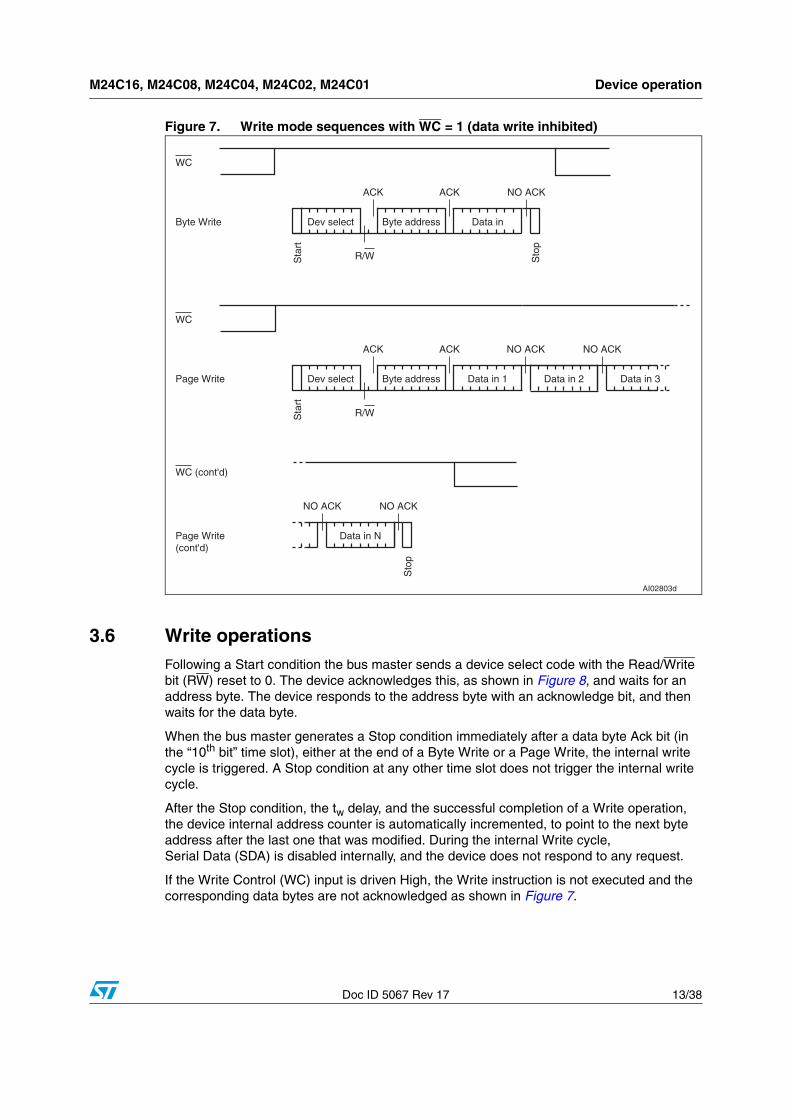
Figure 7. Write mode sequences with WC = 1 (data write inhibited)
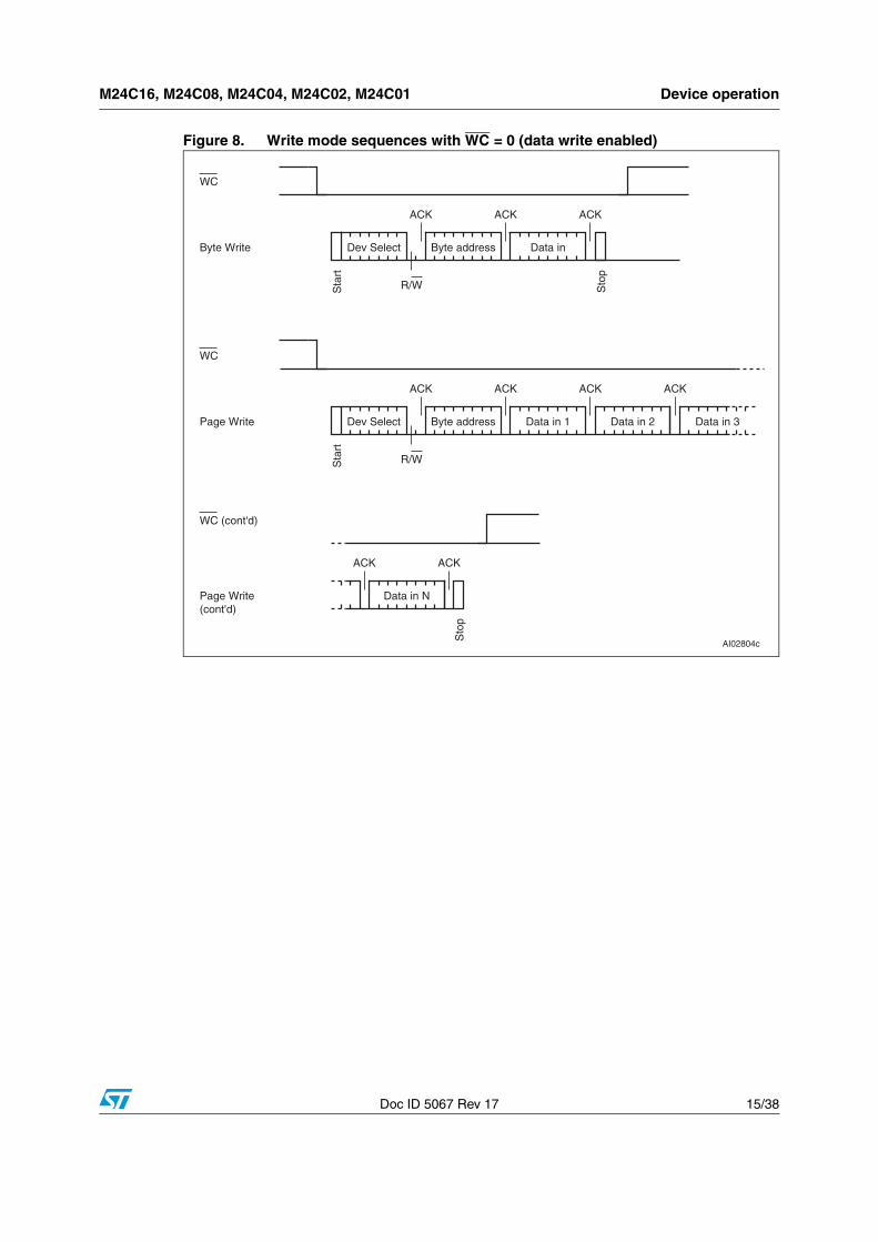
3.6 Write operationsFollowing a Start condition the bus master sends a device select code with the Read/Write bit (RW) reset to 0. The device acknowledges this, as shown in Figure 8, and waits for an address byte. The device responds to the address byte with an acknowledge bit, and then waits for the data byte.
When the bus master generates a Stop condition immediately after a data byte Ack bit (in the “10th bit” time slot), either at the end of a Byte Write or a Page Write, the internal write cycle is triggered. A Stop condition at any other time slot does not trigger the internal write cycle.
After the Stop condition, the tw delay, and the successful completion of a Write operation, the device internal address counter is automatically incremented, to point to the next byte address after the last one that was modified. During the internal Write cycle, Serial Data (SDA) is disabled internally, and the device does not respond to any request.
If the Write Control (WC) input is driven High, the Write instruction is not executed and the corresponding data bytes are not acknowledged as shown in Figure 7.
Sto
p
Sta
rt
Byte Write Dev select Byte address Data in
WC
Sta
rt
Page Write Dev select Byte address Data in 1 Data in 2
WC
Data in 3
AI02803d
Page Write(cont'd)
WC (cont'd)
Sto
p
Data in N
ACK ACK NO ACK
R/W
ACK ACK NO ACK NO ACK
R/W
NO ACK NO ACK
Device operation M24C16, M24C08, M24C04, M24C02, M24C01
14/38 Doc ID 5067 Rev 17
3.6.1 Byte Write
After the device select code and the address byte, the bus master sends one data byte. If the addressed location is Write-protected, by Write Control (WC) being driven High, the device replies to the data byte with NoAck, as shown in Figure 7, and the location is not modified. If, instead, the addressed location is not Write-protected, the device replies with Ack. The bus master terminates the transfer by generating a Stop condition, as shown in Figure 8.
3.6.2 Page Write
The Page Write mode allows up to 16 bytes to be written in a single Write cycle, provided that they are all located in the same page in the memory: that is, the most significant memory address bits are the same. If more bytes are sent than will fit up to the end of the page, a condition known as ‘roll-over’ occurs. This should be avoided, as data starts to become overwritten in an implementation dependent way.
The bus master sends from 1 to 16 bytes of data, each of which is acknowledged by the device if Write Control (WC) is Low. If the addressed location is Write-protected, by Write Control (WC) being driven High, the device replies to the data bytes with NoAck, as shown in Figure 7, and the locations are not modified. After each byte is transferred, the internal byte address counter (the 4 least significant address bits only) is incremented. The transfer is terminated by the bus master generating a Stop condition.
M24C16, M24C08, M24C04, M24C02, M24C01 Device operation
Doc ID 5067 Rev 17 15/38
Figure 8. Write mode sequences with WC = 0 (data write enabled)
Sto
p
Sta
rt
Byte Write Dev Select Byte address Data in
WC
Sta
rt
Page Write Dev Select Byte address Data in 1 Data in 2
WC
Data in 3
AI02804c
Page Write(cont'd)
WC (cont'd)
Sto
p
Data in N
ACK
R/W
ACK ACK
ACK ACK ACK ACK
R/W
ACKACK
Device operation M24C16, M24C08, M24C04, M24C02, M24C01
16/38 Doc ID 5067 Rev 17
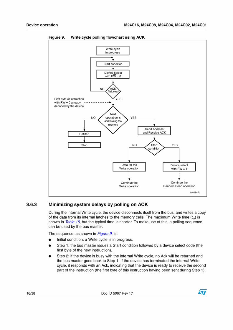
Figure 9. Write cycle polling flowchart using ACK
3.6.3 Minimizing system delays by polling on ACK
During the internal Write cycle, the device disconnects itself from the bus, and writes a copy of the data from its internal latches to the memory cells. The maximum Write time (tw) is shown in Table 15, but the typical time is shorter. To make use of this, a polling sequence can be used by the bus master.
The sequence, as shown in Figure 9, is:
● Initial condition: a Write cycle is in progress.
● Step 1: the bus master issues a Start condition followed by a device select code (thefirst byte of the new instruction).
● Step 2: if the device is busy with the internal Write cycle, no Ack will be returned andthe bus master goes back to Step 1. If the device has terminated the internal Writecycle, it responds with an Ack, indicating that the device is ready to receive the secondpart of the instruction (the first byte of this instruction having been sent during Step 1).
Write cyclein progress
AI01847d
Nextoperation is
addressing thememory
Start condition
Device selectwith RW = 0
ACKReturned
YES
NO
YESNO
ReStart
Stop
Data for theWrite operation
Device selectwith RW = 1
Send Addressand Receive ACK
First byte of instructionwith RW = 0 alreadydecoded by the device
YESNO Startcondition
Continue theWrite operation
Continue theRandom Read operation
M24C16, M24C08, M24C04, M24C02, M24C01 Device operation
Doc ID 5067 Rev 17 17/38
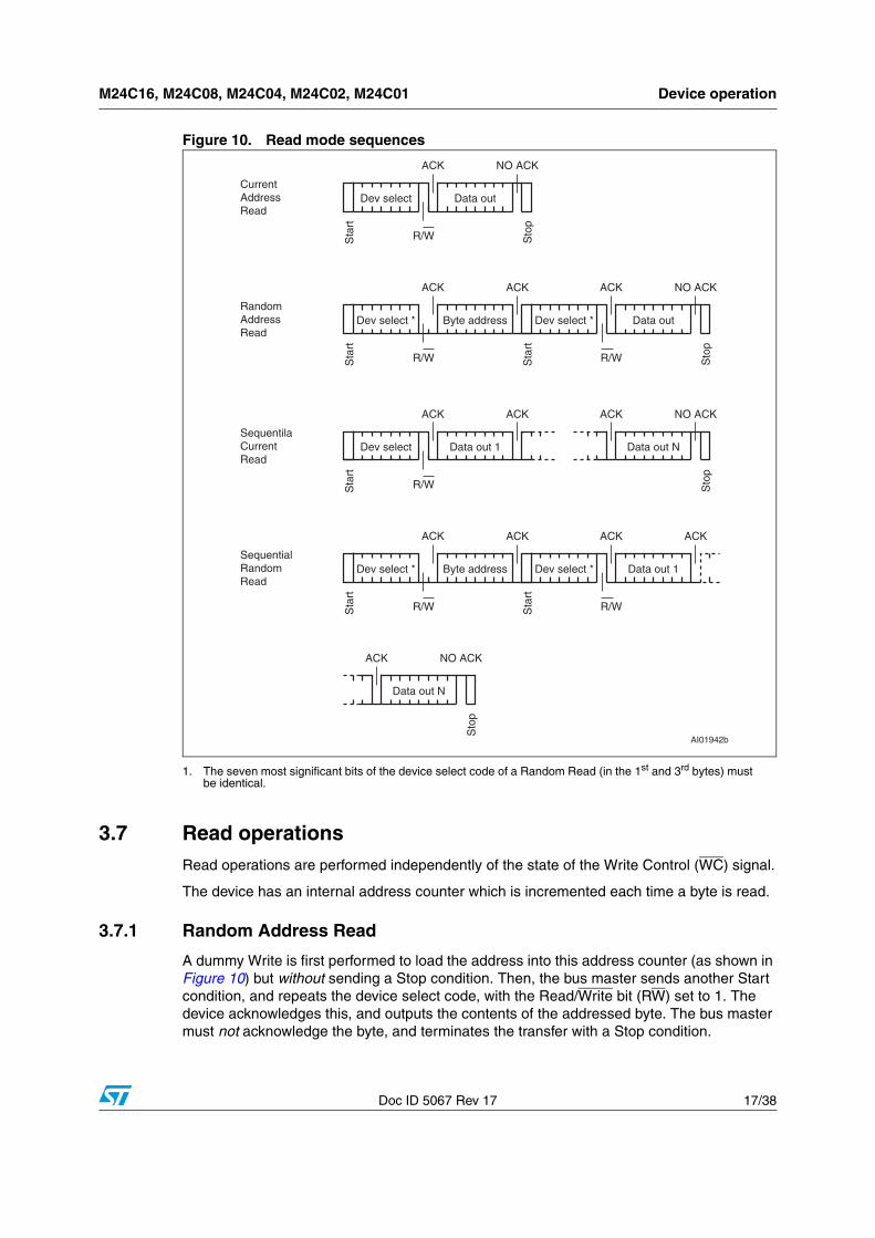
Figure 10. Read mode sequences
1. The seven most significant bits of the device select code of a Random Read (in the 1st and 3rd bytes) must be identical.
3.7 Read operationsRead operations are performed independently of the state of the Write Control (WC) signal.
The device has an internal address counter which is incremented each time a byte is read.
3.7.1 Random Address Read
A dummy Write is first performed to load the address into this address counter (as shown in Figure 10) but without sending a Stop condition. Then, the bus master sends another Start condition, and repeats the device select code, with the Read/Write bit (RW) set to 1. The device acknowledges this, and outputs the contents of the addressed byte. The bus master must not acknowledge the byte, and terminates the transfer with a Stop condition.
Sta
rt
Dev select * Byte address
Sta
rt
Dev select Data out 1
AI01942b
Data out N
Sto
p
Sta
rt
CurrentAddressRead
Dev select Data out
RandomAddressRead
Sto
p
Sta
rt
Dev select * Data out
SequentilaCurrentRead
Sto
p
Data out N
Sta
rt
Dev select * Byte addressSequentialRandomRead
Sta
rt
Dev select * Data out 1
Sto
p
ACK
R/W
NO ACK
ACK
R/W
ACK ACK
R/W
ACK ACK ACK NO ACK
R/W
NO ACK
ACK ACK
R/W
ACK ACK
R/W
ACK NO ACK
Device operation M24C16, M24C08, M24C04, M24C02, M24C01
18/38 Doc ID 5067 Rev 17
3.7.2 Current Address Read
For the Current Address Read operation, following a Start condition, the bus master only sends a device select code with the Read/Write bit (RW) set to 1. The device acknowledges this, and outputs the byte addressed by the internal address counter. The counter is then incremented. The bus master terminates the transfer with a Stop condition, as shown in Figure 10, without acknowledging the byte.
3.7.3 Sequential Read
This operation can be used after a Current Address Read or a Random Address Read. The bus master does acknowledge the data byte output, and sends additional clock pulses so that the device continues to output the next byte in sequence. To terminate the stream of bytes, the bus master must not acknowledge the last byte, and must generate a Stop condition, as shown in Figure 10.
The output data comes from consecutive addresses, with the internal address counter automatically incremented after each byte output. After the last memory address, the address counter ‘rolls-over’, and the device continues to output data from memory address 00h.
3.7.4 Acknowledge in Read mode
For all Read commands, the device waits, after each byte read, for an acknowledgment during the 9th bit time. If the bus master does not drive Serial Data (SDA) Low during this time, the device terminates the data transfer and switches to its Standby mode.
M24C16, M24C08, M24C04, M24C02, M24C01 Initial delivery state
Doc ID 5067 Rev 17 19/38
4 Initial delivery state
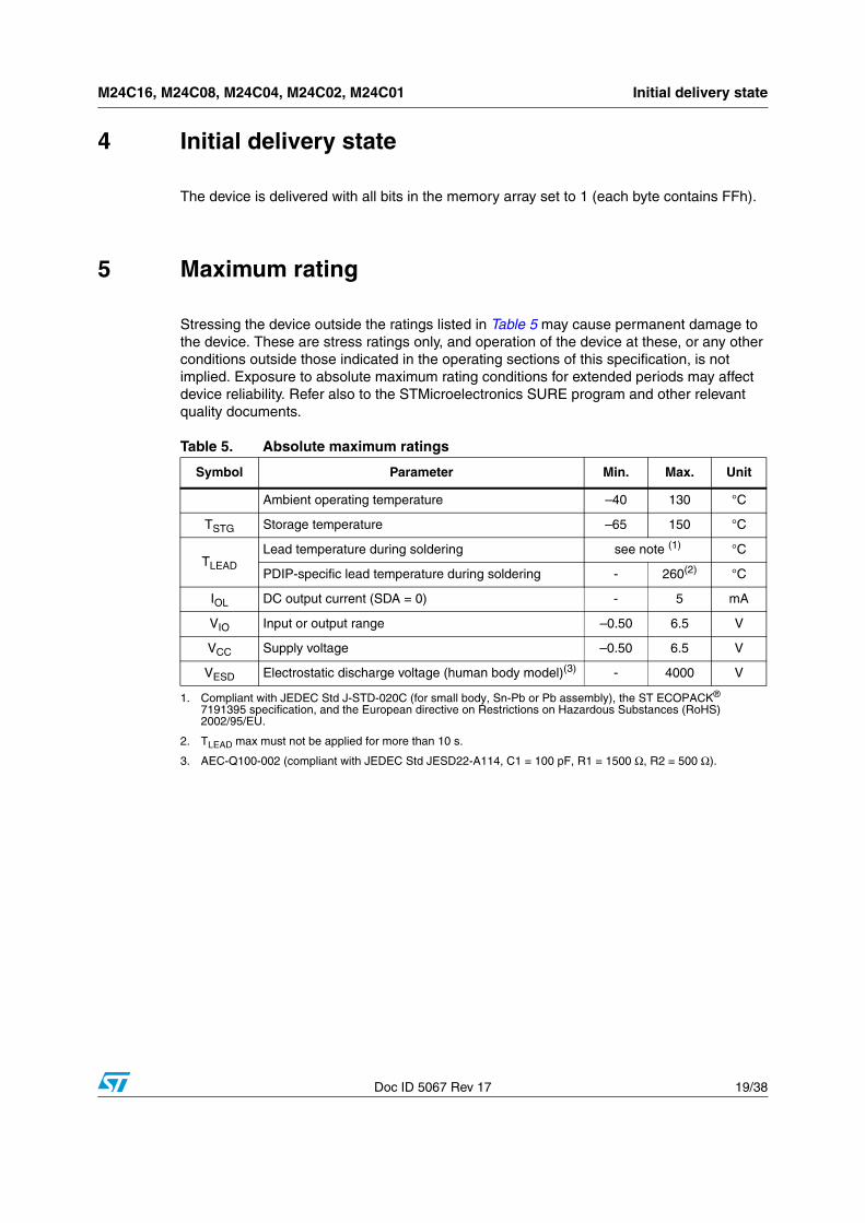
The device is delivered with all bits in the memory array set to 1 (each byte contains FFh).
5 Maximum rating
Stressing the device outside the ratings listed in Table 5 may cause permanent damage to the device. These are stress ratings only, and operation of the device at these, or any other conditions outside those indicated in the operating sections of this specification, is not implied. Exposure to absolute maximum rating conditions for extended periods may affect device reliability. Refer also to the STMicroelectronics SURE program and other relevant quality documents.
Table 5. Absolute maximum ratings
Symbol Parameter Min. Max. Unit
Ambient operating temperature –40 130 °C
TSTG Storage temperature –65 150 °C
TLEAD
Lead temperature during soldering see note (1)
1. Compliant with JEDEC Std J-STD-020C (for small body, Sn-Pb or Pb assembly), the ST ECOPACK® 7191395 specification, and the European directive on Restrictions on Hazardous Substances (RoHS) 2002/95/EU.
°C
PDIP-specific lead temperature during soldering - 260(2)
2. TLEAD max must not be applied for more than 10 s.
°C
IOL DC output current (SDA = 0) - 5 mA
VIO Input or output range –0.50 6.5 V
VCC Supply voltage –0.50 6.5 V
VESD Electrostatic discharge voltage (human body model)(3)
3. AEC-Q100-002 (compliant with JEDEC Std JESD22-A114, C1 = 100 pF, R1 = 1500 Ω, R2 = 500 Ω).
- 4000 V
DC and AC parameters M24C16, M24C08, M24C04, M24C02, M24C01
20/38 Doc ID 5067 Rev 17
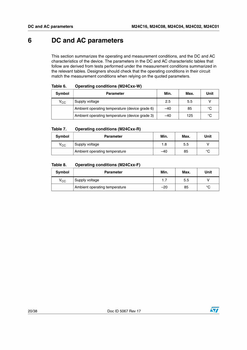
6 DC and AC parameters
This section summarizes the operating and measurement conditions, and the DC and AC characteristics of the device. The parameters in the DC and AC characteristic tables that follow are derived from tests performed under the measurement conditions summarized in the relevant tables. Designers should check that the operating conditions in their circuit match the measurement conditions when relying on the quoted parameters.
Table 6. Operating conditions (M24Cxx-W)
Symbol Parameter Min. Max. Unit
VCC Supply voltage 2.5 5.5 V
Ambient operating temperature (device grade 6) –40 85 °C
Ambient operating temperature (device grade 3) –40 125 °C
Table 7. Operating conditions (M24Cxx-R)
Symbol Parameter Min. Max. Unit
VCC Supply voltage 1.8 5.5 V
Ambient operating temperature –40 85 °C
Table 8. Operating conditions (M24Cxx-F)
Symbol Parameter Min. Max. Unit
VCC Supply voltage 1.7 5.5 V
Ambient operating temperature –20 85 °C
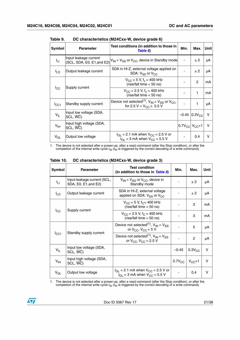
M24C16, M24C08, M24C04, M24C02, M24C01 DC and AC parameters
Doc ID 5067 Rev 17 21/38
Table 9. DC characteristics (M24Cxx-W, device grade 6)
Symbol ParameterTest conditions (in addition to those in
Table 6)Min. Max. Unit
ILIInput leakage current (SCL, SDA, E0, E1,and E2)
VIN = VSS or VCC, device in Standby mode - ± 2 µA
ILO Output leakage currentSDA in Hi-Z, external voltage applied on
SDA: VSS or VCC- ± 2 µA
ICC Supply current
VCC = 5 V, fc = 400 kHz(rise/fall time < 50 ns)
- 2 mA
VCC = 2.5 V, fc = 400 kHz(rise/fall time < 50 ns)
- 1 mA
ICC1 Standby supply currentDevice not selected(1), VIN = VSS or VCC,
for 2.5 V < VCC ≤ 5.5 V
1. The device is not selected after a power-up, after a read command (after the Stop condition), or after the completion of the internal write cycle tW (tW is triggered by the correct decoding of a write command).
- 1 µA
VILInput low voltage (SDA, SCL, WC)
–0.45 0.3VCC V
VIHInput high voltage (SDA, SCL, WC)
0.7VCC VCC+1 V
VOL Output low voltageIOL = 2.1 mA when VCC = 2.5 V or
IOL = 3 mA when VCC = 5.5 V- 0.4 V
Table 10. DC characteristics (M24Cxx-W, device grade 3)
Symbol ParameterTest condition
(in addition to those in Table 6)Min. Max. Unit
ILIInput leakage current (SCL, SDA, E0, E1,and E2)
VIN = VSS or VCC, device in Standby mode
- ± 2 µA
ILO Output leakage currentSDA in Hi-Z, external voltage applied on SDA: VSS or VCC
- ± 2 µA
ICC Supply current
VCC = 5 V, fC= 400 kHz(rise/fall time < 50 ns)
- 3 mA
VCC = 2.5 V, fC = 400 kHz (rise/fall time < 50 ns)
- 3 mA
ICC1 Standby supply current
Device not selected(1), VIN = VSS or VCC, VCC = 5 V
1. The device is not selected after a power-up, after a read command (after the Stop condition), or after the completion of the internal write cycle tW (tW is triggered by the correct decoding of a write command).
- 5 µA
Device not selected(1), VIN = VSS or VCC, VCC = 2.5 V
- 2 µA
VILInput low voltage (SDA, SCL, WC)
–0.45 0.3VCC V
VIHInput high voltage (SDA, SCL, WC)
0.7VCC VCC+1 V
VOL Output low voltageIOL = 2.1 mA when VCC = 2.5 V or
IOL = 3 mA when VCC = 5.5 V- 0.4 V
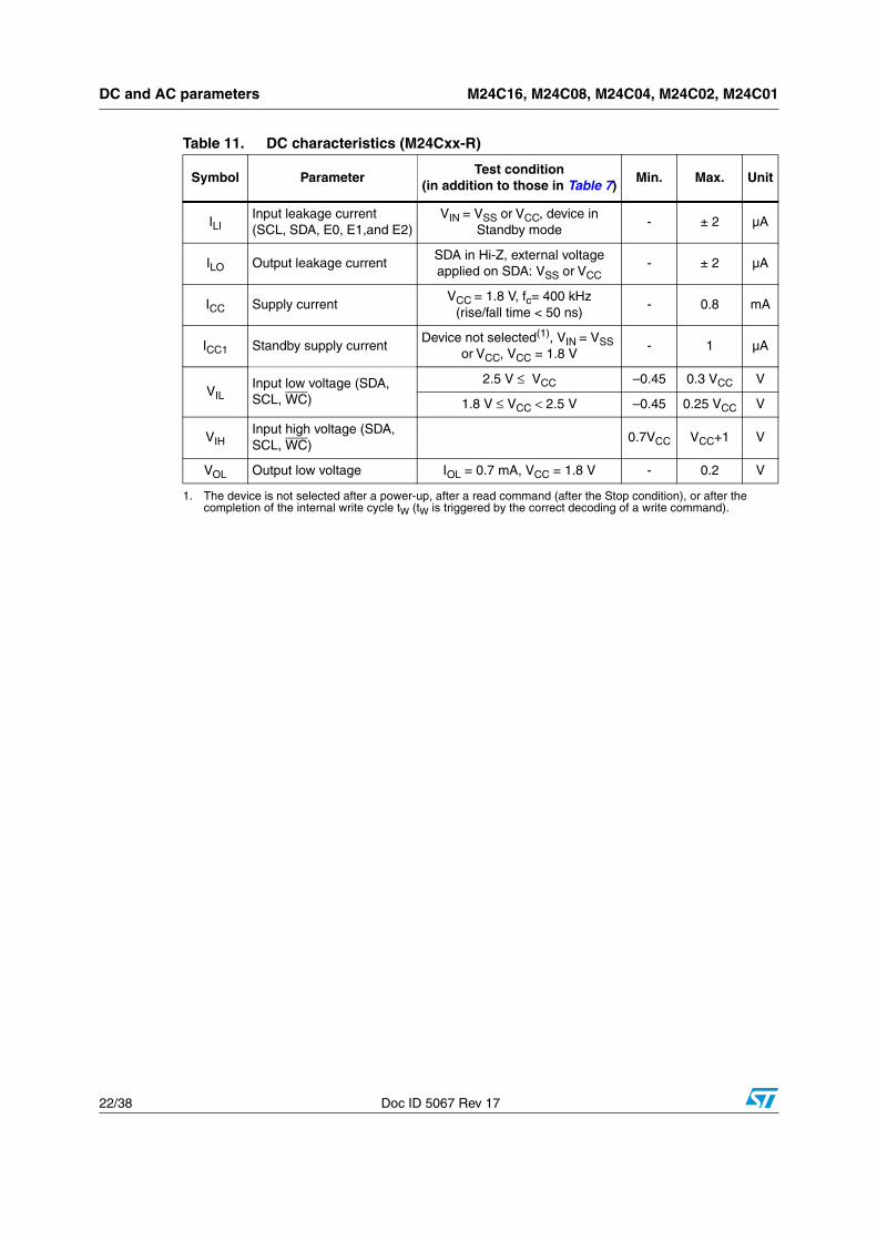
DC and AC parameters M24C16, M24C08, M24C04, M24C02, M24C01
22/38 Doc ID 5067 Rev 17
Table 11. DC characteristics (M24Cxx-R)
Symbol ParameterTest condition
(in addition to those in Table 7)Min. Max. Unit
ILIInput leakage current (SCL, SDA, E0, E1,and E2)
VIN = VSS or VCC, device in Standby mode
- ± 2 µA
ILO Output leakage currentSDA in Hi-Z, external voltage applied on SDA: VSS or VCC
- ± 2 µA
ICC Supply currentVCC = 1.8 V, fc= 400 kHz
(rise/fall time < 50 ns)- 0.8 mA
ICC1 Standby supply currentDevice not selected(1), VIN = VSS
or VCC, VCC = 1.8 V
1. The device is not selected after a power-up, after a read command (after the Stop condition), or after the completion of the internal write cycle tW (tW is triggered by the correct decoding of a write command).
- 1 µA
VILInput low voltage (SDA, SCL, WC)
2.5 V ≤ VCC –0.45 0.3 VCC V
1.8 V ≤ VCC < 2.5 V –0.45 0.25 VCC V
VIHInput high voltage (SDA, SCL, WC)
0.7VCC VCC+1 V
VOL Output low voltage IOL = 0.7 mA, VCC = 1.8 V - 0.2 V
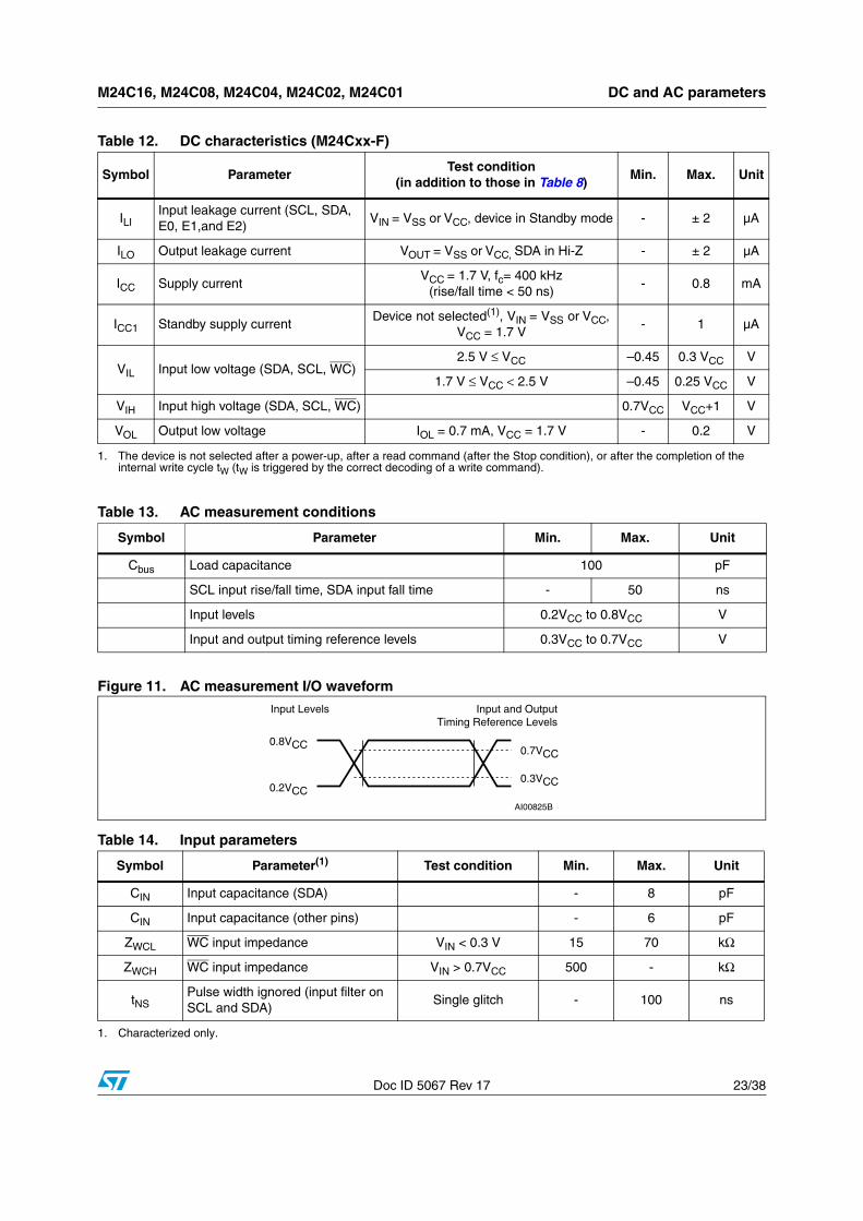
M24C16, M24C08, M24C04, M24C02, M24C01 DC and AC parameters
Doc ID 5067 Rev 17 23/38
Figure 11. AC measurement I/O waveform
Table 12. DC characteristics (M24Cxx-F)
Symbol ParameterTest condition
(in addition to those in Table 8)Min. Max. Unit
ILIInput leakage current (SCL, SDA, E0, E1,and E2)
VIN = VSS or VCC, device in Standby mode - ± 2 µA
ILO Output leakage current VOUT = VSS or VCC, SDA in Hi-Z - ± 2 µA
ICC Supply currentVCC = 1.7 V, fc= 400 kHz
(rise/fall time < 50 ns)- 0.8 mA
ICC1 Standby supply currentDevice not selected(1), VIN = VSS or VCC,
VCC = 1.7 V- 1 µA
VIL Input low voltage (SDA, SCL, WC)2.5 V ≤ VCC –0.45 0.3 VCC V
1.7 V ≤ VCC < 2.5 V –0.45 0.25 VCC V
VIH Input high voltage (SDA, SCL, WC) 0.7VCC VCC+1 V
VOL Output low voltage IOL = 0.7 mA, VCC = 1.7 V - 0.2 V
1. The device is not selected after a power-up, after a read command (after the Stop condition), or after the completion of theinternal write cycle tW (tW is triggered by the correct decoding of a write command).
Table 13. AC measurement conditions
Symbol Parameter Min. Max. Unit
Cbus Load capacitance 100 pF
SCL input rise/fall time, SDA input fall time - 50 ns
Input levels 0.2VCC to 0.8VCC V
Input and output timing reference levels 0.3VCC to 0.7VCC V
AI00825B
0.8VCC
0.2VCC
0.7VCC
0.3VCC
Input and OutputTiming Reference Levels
Input Levels
Table 14. Input parameters
Symbol Parameter(1) Test condition Min. Max. Unit
CIN Input capacitance (SDA) - 8 pF
CIN Input capacitance (other pins) - 6 pF
ZWCL WC input impedance VIN < 0.3 V 15 70 kΩ
ZWCH WC input impedance VIN > 0.7VCC 500 - kΩ
tNSPulse width ignored (input filter on SCL and SDA)
Single glitch - 100 ns
1. Characterized only.
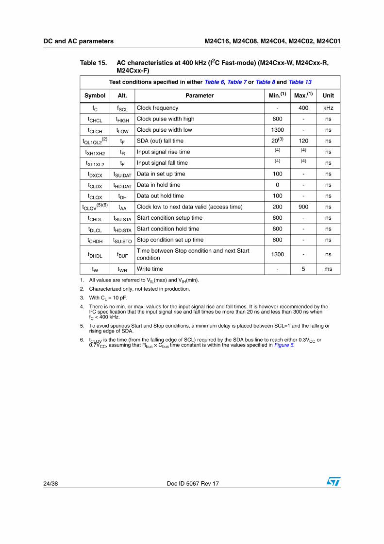
DC and AC parameters M24C16, M24C08, M24C04, M24C02, M24C01
24/38 Doc ID 5067 Rev 17
Table 15. AC characteristics at 400 kHz (I2C Fast-mode) (M24Cxx-W, M24Cxx-R, M24Cxx-F)
Test conditions specified in either Table 6, Table 7 or Table 8 and Table 13
Symbol Alt. Parameter Min.(1)
1. All values are referred to VIL(max) and VIH(min).
Max.(1) Unit
fC fSCL Clock frequency - 400 kHz
tCHCL tHIGH Clock pulse width high 600 - ns
tCLCH tLOW Clock pulse width low 1300 - ns
tQL1QL2(2)
2. Characterized only, not tested in production.
tF SDA (out) fall time 20(3)
3. With CL = 10 pF.
120 ns
tXH1XH2 tR Input signal rise time (4)
4. There is no min. or max. values for the input signal rise and fall times. It is however recommended by the I²C specification that the input signal rise and fall times be more than 20 ns and less than 300 ns when fC < 400 kHz.
(4) ns
tXL1XL2 tF Input signal fall time (4) (4) ns
tDXCX tSU:DAT Data in set up time 100 - ns
tCLDX tHD:DAT Data in hold time 0 - ns
tCLQX tDH Data out hold time 100 - ns
tCLQV(5)(6)
5. To avoid spurious Start and Stop conditions, a minimum delay is placed between SCL=1 and the falling or rising edge of SDA.
6. tCLQV is the time (from the falling edge of SCL) required by the SDA bus line to reach either 0.3VCC or 0.7VCC, assuming that Rbus × Cbus time constant is within the values specified in Figure 5.
tAA Clock low to next data valid (access time) 200 900 ns
tCHDL tSU:STA Start condition setup time 600 - ns
tDLCL tHD:STA Start condition hold time 600 - ns
tCHDH tSU:STO Stop condition set up time 600 - ns
tDHDL tBUFTime between Stop condition and next Start condition
1300 - ns
tW tWR Write time - 5 ms
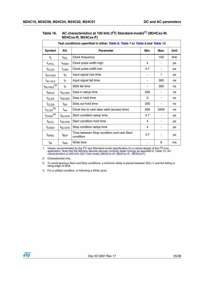
M24C16, M24C08, M24C04, M24C02, M24C01 DC and AC parameters
Doc ID 5067 Rev 17 25/38
Table 16. AC characteristics at 100 kHz (I2C Standard-mode)(1) (M24Cxx-W, M24Cxx-R, M24Cxx-F)
1. Values recommended by the I2C bus Standard-mode specification for a robust design of the I2C bus application. Note that the M24xxx devices decode correctly faster timings as specified in Table 15: AC characteristics at 400 kHz (I2C Fast-mode) (M24Cxx-W, M24Cxx-R, M24Cxx-F).
Test conditions specified in either Table 6, Table 7 or Table 8 and Table 13
Symbol Alt. Parameter Min. Max. Unit
fC fSCL Clock frequency - 100 kHz
tCHCL tHIGH Clock pulse width high 4 - µs
tCLCH tLOW Clock pulse width low 4.7 - µs
tXH1XH2 tR Input signal rise time - 1 µs
tXL1XL2 tF Input signal fall time - 300 ns
tQL1QL2(2)
2. Characterized only.
tF SDA fall time - 300 ns
tDXCX tSU:DAT Data in setup time 250 - ns
tCLDX tHD:DAT Data in hold time 0 - ns
tCLQX tDH Data out hold time 200 - ns
tCLQV(3)
3. To avoid spurious Start and Stop conditions, a minimum delay is placed between SCL=1 and the falling or rising edge of SDA.
tAA Clock low to next data valid (access time) 200 3450 ns
tCHDX(4)
4. For a reStart condition, or following a Write cycle.
tSU:STA Start condition setup time 4.7 - µs
tDLCL tHD:STA Start condition hold time 4 - µs
tCHDH tSU:STO Stop condition setup time 4 - µs
tDHDL tBUFTime between Stop condition and next Start condition
4.7 - µs
tW tWR Write time - 5 ms
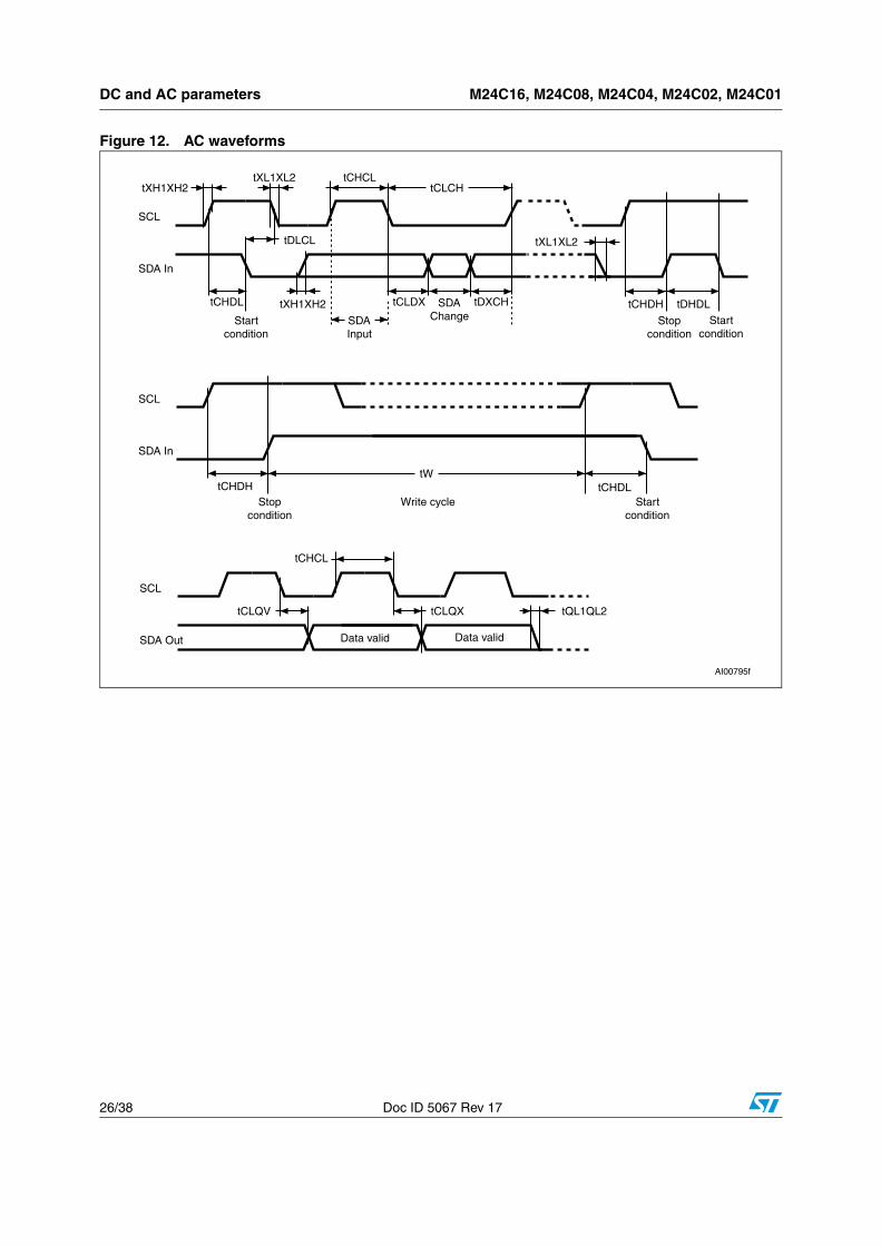
DC and AC parameters M24C16, M24C08, M24C04, M24C02, M24C01
26/38 Doc ID 5067 Rev 17
Figure 12. AC waveforms
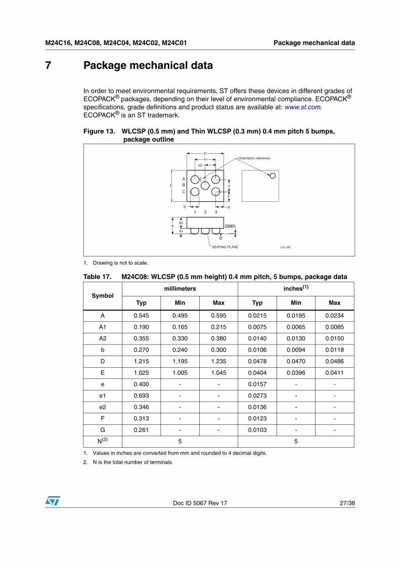
M24C16, M24C08, M24C04, M24C02, M24C01 Package mechanical data
Doc ID 5067 Rev 17 27/38
7 Package mechanical data
In order to meet environmental requirements, ST offers these devices in different grades of ECOPACK® packages, depending on their level of environmental compliance. ECOPACK® specifications, grade definitions and product status are available at: www.st.com. ECOPACK® is an ST trademark.
Figure 13. WLCSP (0.5 mm) and Thin WLCSP (0.3 mm) 0.4 mm pitch 5 bumps, package outline
1. Drawing is not to scale.
Table 17. M24C08: WLCSP (0.5 mm height) 0.4 mm pitch, 5 bumps, package data
Symbolmillimeters inches(1)
1. Values in inches are converted from mm and rounded to 4 decimal digits.
Typ Min Max Typ Min Max
A 0.545 0.495 0.595 0.0215 0.0195 0.0234
A1 0.190 0.165 0.215 0.0075 0.0065 0.0085
A2 0.355 0.330 0.380 0.0140 0.0130 0.0150
b 0.270 0.240 0.300 0.0106 0.0094 0.0118
D 1.215 1.195 1.235 0.0478 0.0470 0.0486
E 1.025 1.005 1.045 0.0404 0.0396 0.0411
e 0.400 - - 0.0157 - -
e1 0.693 - - 0.0273 - -
e2 0.346 - - 0.0136 - -
F 0.313 - - 0.0123 - -
G 0.261 - - 0.0103 - -
N(2)
2. N is the total number of terminals.
5 5
Orientation reference
E
A
B
C
D
e1
e2
e
F
G
AA2
A1
SEATING PLANE
1 2 3
1Ca_ME
b
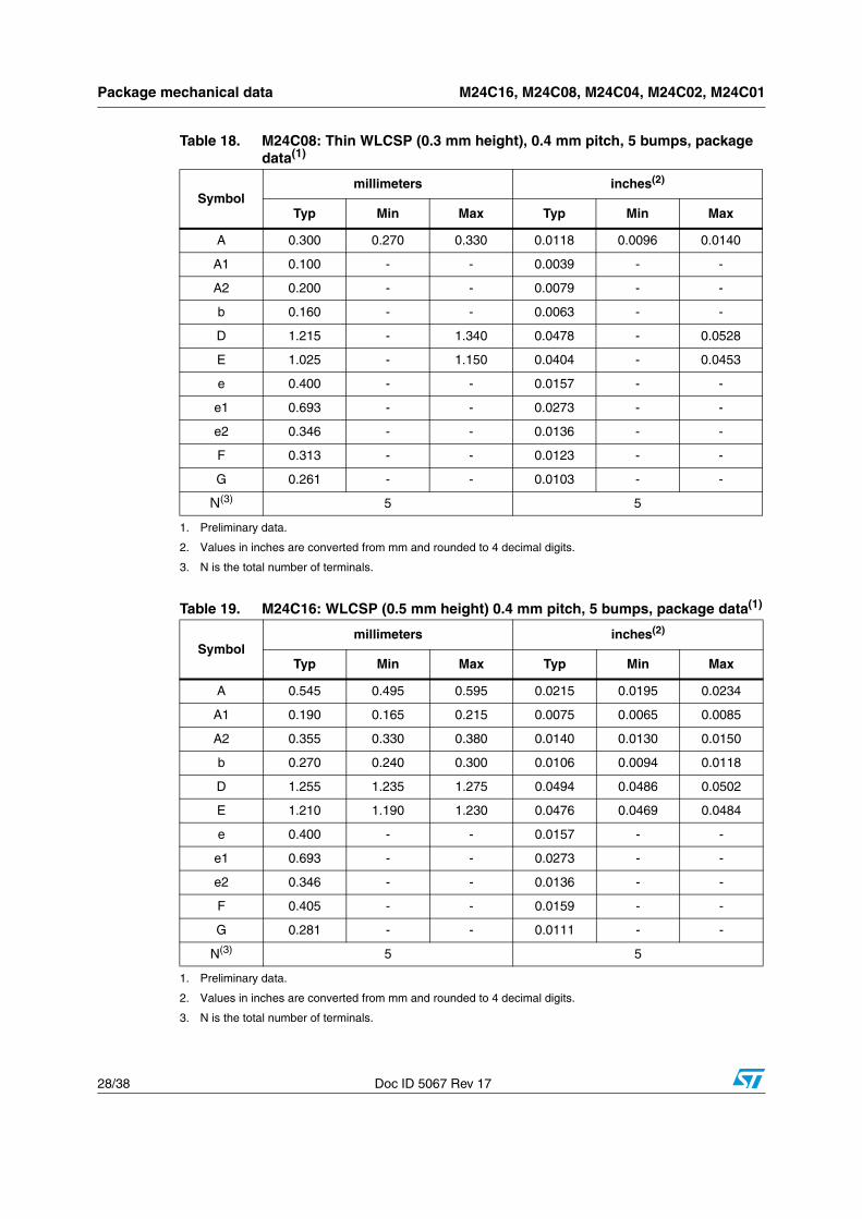
Package mechanical data M24C16, M24C08, M24C04, M24C02, M24C01
28/38 Doc ID 5067 Rev 17
Table 18. M24C08: Thin WLCSP (0.3 mm height), 0.4 mm pitch, 5 bumps, package data(1)
1. Preliminary data.
Symbolmillimeters inches(2)
2. Values in inches are converted from mm and rounded to 4 decimal digits.
Typ Min Max Typ Min Max
A 0.300 0.270 0.330 0.0118 0.0096 0.0140
A1 0.100 - - 0.0039 - -
A2 0.200 - - 0.0079 - -
b 0.160 - - 0.0063 - -
D 1.215 - 1.340 0.0478 - 0.0528
E 1.025 - 1.150 0.0404 - 0.0453
e 0.400 - - 0.0157 - -
e1 0.693 - - 0.0273 - -
e2 0.346 - - 0.0136 - -
F 0.313 - - 0.0123 - -
G 0.261 - - 0.0103 - -
N(3)
3. N is the total number of terminals.
5 5
Table 19. M24C16: WLCSP (0.5 mm height) 0.4 mm pitch, 5 bumps, package data(1)
1. Preliminary data.
Symbolmillimeters inches(2)
2. Values in inches are converted from mm and rounded to 4 decimal digits.
Typ Min Max Typ Min Max
A 0.545 0.495 0.595 0.0215 0.0195 0.0234
A1 0.190 0.165 0.215 0.0075 0.0065 0.0085
A2 0.355 0.330 0.380 0.0140 0.0130 0.0150
b 0.270 0.240 0.300 0.0106 0.0094 0.0118
D 1.255 1.235 1.275 0.0494 0.0486 0.0502
E 1.210 1.190 1.230 0.0476 0.0469 0.0484
e 0.400 - - 0.0157 - -
e1 0.693 - - 0.0273 - -
e2 0.346 - - 0.0136 - -
F 0.405 - - 0.0159 - -
G 0.281 - - 0.0111 - -
N(3)
3. N is the total number of terminals.
5 5
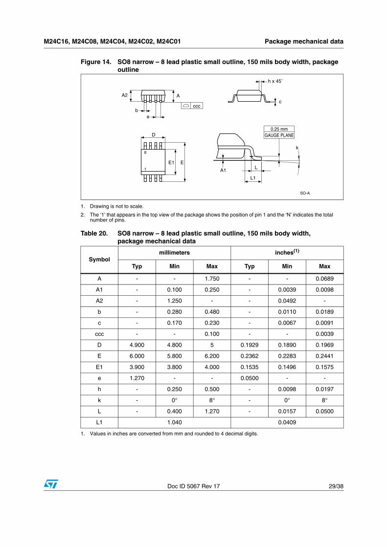
M24C16, M24C08, M24C04, M24C02, M24C01 Package mechanical data
Doc ID 5067 Rev 17 29/38
Figure 14. SO8 narrow – 8 lead plastic small outline, 150 mils body width, package outline
1. Drawing is not to scale.
2. The ‘1’ that appears in the top view of the package shows the position of pin 1 and the ‘N’ indicates the total number of pins.
Table 20. SO8 narrow – 8 lead plastic small outline, 150 mils body width, package mechanical data
Symbolmillimeters inches(1)
1. Values in inches are converted from mm and rounded to 4 decimal digits.
Typ Min Max Typ Min Max
A - - 1.750 - - 0.0689
A1 - 0.100 0.250 - 0.0039 0.0098
A2 - 1.250 - - 0.0492 -
b - 0.280 0.480 - 0.0110 0.0189
c - 0.170 0.230 - 0.0067 0.0091
ccc - - 0.100 - - 0.0039
D 4.900 4.800 5 0.1929 0.1890 0.1969
E 6.000 5.800 6.200 0.2362 0.2283 0.2441
E1 3.900 3.800 4.000 0.1535 0.1496 0.1575
e 1.270 - - 0.0500 - -
h - 0.250 0.500 - 0.0098 0.0197
k - 0° 8° - 0° 8°
L - 0.400 1.270 - 0.0157 0.0500
L1 1.040 0.0409
SO-A
E1
8
cccb
e
A
D
c
1
E
h x 45˚
A2
k
0.25 mm
L
L1
A1
GAUGE PLANE
Package mechanical data M24C16, M24C08, M24C04, M24C02, M24C01
30/38 Doc ID 5067 Rev 17
Figure 15. UFDFPN8 (MLP8) 8-lead ultra thin fine pitch dual flat package no lead 2 x 3 mm, outline
1. Drawing is not to scale.
2. The central pad (the area E2 by D2 in the above illustration) is pulled, internally, to VSS. It must not be allowed to be connected to any other voltage or signal line on the PCB, for example during the soldering process.
3. The circle in the top view of the package indicates the position of pin 1.
Table 21. UFDFPN8 (MLP8) 8-lead ultra thin fine pitch dual flat package no lead 2 x 3 mm, data
Symbolmillimeters inches(1)
1. Values in inches are converted from mm and rounded to 4 decimal digits.
Note
Typ Min Max Typ Min Max
A 0.550 0.450 0.600 0.0217 0.0177 0.0236
A1 0.020 0.000 0.050 0.0008 0.0000 0.0020
b 0.250 0.200 0.300 0.0098 0.0079 0.0118
D 2.000 1.900 2.100 0.0787 0.0748 0.0827
D2 (MB) 1.600 1.500 1.700 0.0630 0.0591 0.0669
D2 (MC) - 1.200 1.600 - 0.0472 0.0630
E 3.000 2.900 3.100 0.1181 0.1142 0.1220
E2 (MB) 0.200 0.100 0.300 0.0079 0.0039 0.0118
E2 (MC) - 1.200 1.600 - 0.0472 0.0630
e 0.500 - - 0.0197 - -
K - 0.300 - - 0.0118 -
L - 0.300 0.500 - 0.0118 0.0197
L1 - 0.150 - - 0.0059
L3 - 0.300 - - 0.0118 -
eee 0.080 0.0031 (2)
2. Applied for exposed die paddle and terminals. Excludes embedding part of exposed die paddle from measuring.
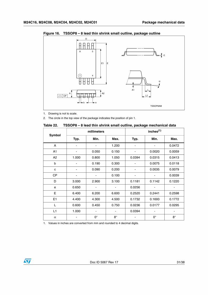
M24C16, M24C08, M24C04, M24C02, M24C01 Package mechanical data
Doc ID 5067 Rev 17 31/38
Figure 16. TSSOP8 – 8 lead thin shrink small outline, package outline
1. Drawing is not to scale.
2. The circle in the top view of the package indicates the position of pin 1.
Table 22. TSSOP8 – 8 lead thin shrink small outline, package mechanical data
Symbolmillimeters inches(1)
1. Values in inches are converted from mm and rounded to 4 decimal digits.
Typ. Min. Max. Typ. Min. Max.
A - - 1.200 - - 0.0472
A1 - 0.050 0.150 - 0.0020 0.0059
A2 1.000 0.800 1.050 0.0394 0.0315 0.0413
b - 0.190 0.300 - 0.0075 0.0118
c - 0.090 0.200 - 0.0035 0.0079
CP - - 0.100 - - 0.0039
D 3.000 2.900 3.100 0.1181 0.1142 0.1220
e 0.650 - - 0.0256 - -
E 6.400 6.200 6.600 0.2520 0.2441 0.2598
E1 4.400 4.300 4.500 0.1732 0.1693 0.1772
L 0.600 0.450 0.750 0.0236 0.0177 0.0295
L1 1.000 - - 0.0394 - -
α - 0° 8° - 0° 8°
TSSOP8AM
1
8
CP
c
L
EE1
D
A2A
α
eb
4
5
A1
L1
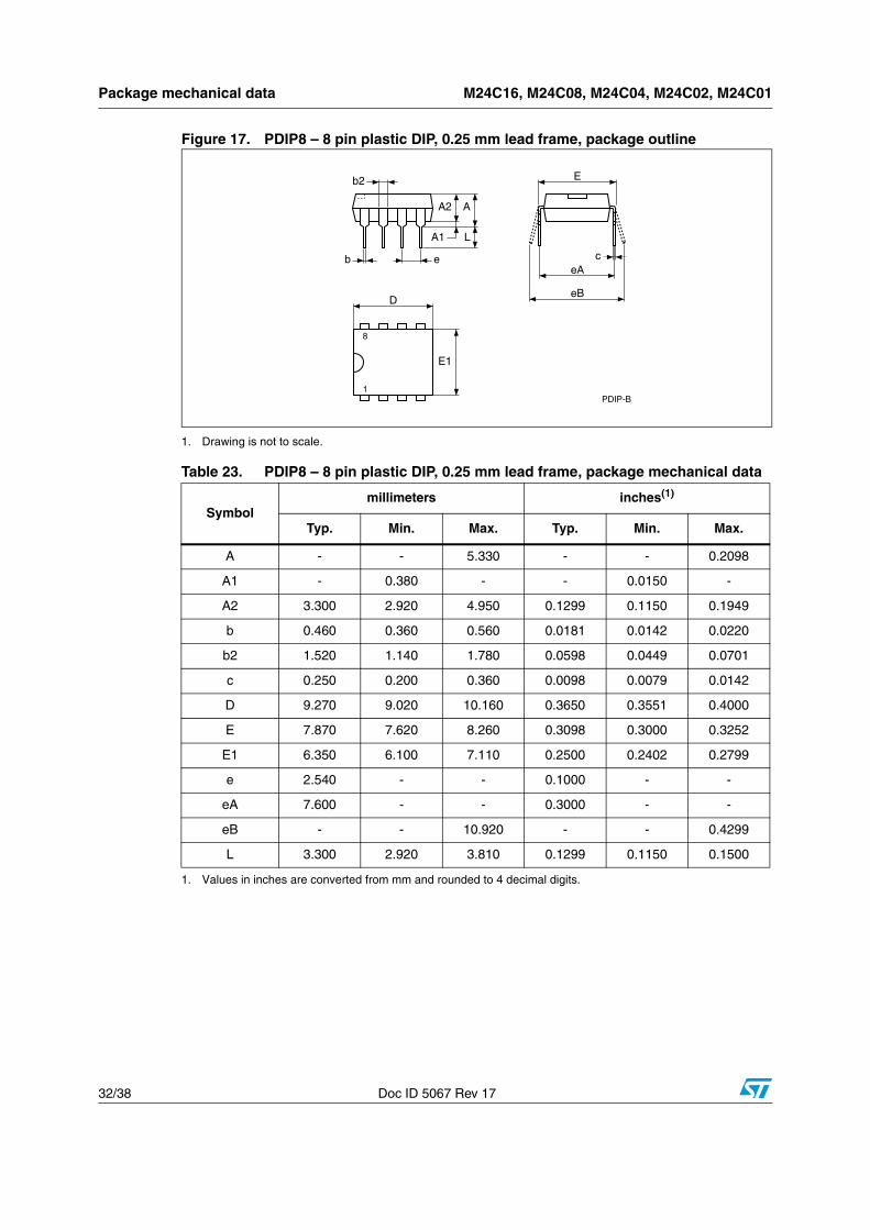
Package mechanical data M24C16, M24C08, M24C04, M24C02, M24C01
32/38 Doc ID 5067 Rev 17
Figure 17. PDIP8 – 8 pin plastic DIP, 0.25 mm lead frame, package outline
1. Drawing is not to scale.
Table 23. PDIP8 – 8 pin plastic DIP, 0.25 mm lead frame, package mechanical data
Symbolmillimeters inches(1)
1. Values in inches are converted from mm and rounded to 4 decimal digits.
Typ. Min. Max. Typ. Min. Max.
A - - 5.330 - - 0.2098
A1 - 0.380 - - 0.0150 -
A2 3.300 2.920 4.950 0.1299 0.1150 0.1949
b 0.460 0.360 0.560 0.0181 0.0142 0.0220
b2 1.520 1.140 1.780 0.0598 0.0449 0.0701
c 0.250 0.200 0.360 0.0098 0.0079 0.0142
D 9.270 9.020 10.160 0.3650 0.3551 0.4000
E 7.870 7.620 8.260 0.3098 0.3000 0.3252
E1 6.350 6.100 7.110 0.2500 0.2402 0.2799
e 2.540 - - 0.1000 - -
eA 7.600 - - 0.3000 - -
eB - - 10.920 - - 0.4299
L 3.300 2.920 3.810 0.1299 0.1150 0.1500
PDIP-B
A2
A1
A
L
b e
D
E1
8
1
ceA
b2
eB
E
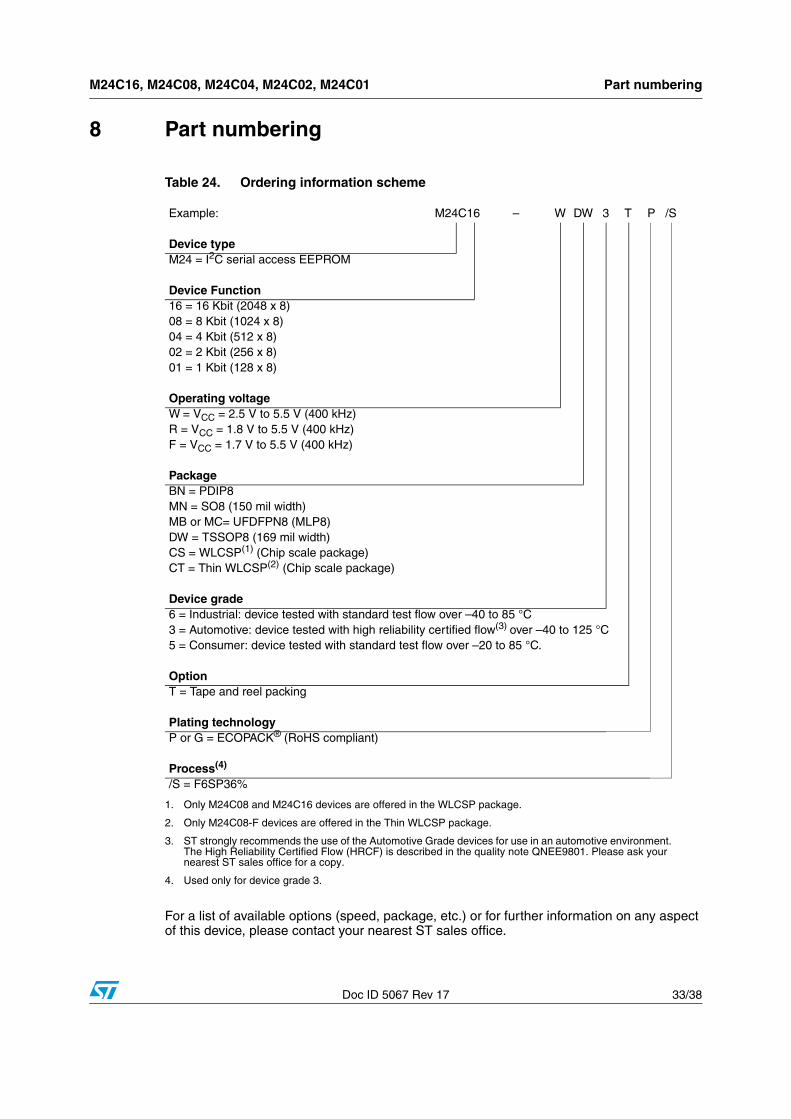
M24C16, M24C08, M24C04, M24C02, M24C01 Part numbering
Doc ID 5067 Rev 17 33/38
8 Part numbering
For a list of available options (speed, package, etc.) or for further information on any aspect of this device, please contact your nearest ST sales office.
Table 24. Ordering information scheme Example: M24C16 – W DW 3 T P /S
Device typeM24 = I2C serial access EEPROM
Device Function16 = 16 Kbit (2048 x 8)08 = 8 Kbit (1024 x 8)04 = 4 Kbit (512 x 8)02 = 2 Kbit (256 x 8)01 = 1 Kbit (128 x 8)
Operating voltageW = VCC = 2.5 V to 5.5 V (400 kHz)R = VCC = 1.8 V to 5.5 V (400 kHz)F = VCC = 1.7 V to 5.5 V (400 kHz)
PackageBN = PDIP8MN = SO8 (150 mil width)MB or MC= UFDFPN8 (MLP8)DW = TSSOP8 (169 mil width)CS = WLCSP(1) (Chip scale package)
1. Only M24C08 and M24C16 devices are offered in the WLCSP package.
CT = Thin WLCSP(2) (Chip scale package)
2. Only M24C08-F devices are offered in the Thin WLCSP package.
Device grade6 = Industrial: device tested with standard test flow over –40 to 85 °C3 = Automotive: device tested with high reliability certified flow(3) over –40 to 125 °C
3. ST strongly recommends the use of the Automotive Grade devices for use in an automotive environment. The High Reliability Certified Flow (HRCF) is described in the quality note QNEE9801. Please ask your nearest ST sales office for a copy.
5 = Consumer: device tested with standard test flow over –20 to 85 °C.
OptionT = Tape and reel packing
Plating technologyP or G = ECOPACK® (RoHS compliant)
Process(4)
4. Used only for device grade 3.
/S = F6SP36%
Revision history M24C16, M24C08, M24C04, M24C02, M24C01
34/38 Doc ID 5067 Rev 17
9 Revision history
Table 25. Document revision history
Date Version Changes
10-Dec-1999 2.4TSSOP8 Turned-Die package removed (p 2 and order information)
Lead temperature added for TSSOP8 in table 2
18-Apr-2000 2.5Labelling change to Fig-2D, correction of values for ‘E’ and main caption for Tab-13
05-May-2000 2.6 Extra labelling to Fig-2D
23-Nov-2000 3.0SBGA package information removed to an annex document
-R range changed to being the -S range, and the new -R range added
19-Feb-2001 3.1
SBGA package information put back in this document
Lead Soldering Temperature in the Absolute Maximum Ratings table amended
Write Cycle Polling Flow Chart using ACK illustration updated
References to PSDIP changed to PDIP and Package Mechanical data updated
Wording brought in to line with standard glossary
20-Apr-2001 3.2 Revision of DC and AC characteristics for the -S series
08-Oct-2001 3.3Ball numbers added to the SBGA connections and package mechanical illustrations
09-Nov-2001 3.4Specification of Test Condition for Leakage Currents in the DC Characteristics table improved
30-Jul-2002 3.5Document reformatted using new template. SBGA5 package removed
TSSOP8 (3x3mm² body size) package (MSOP8) added. -L voltage range added
04-Feb-2003 3.6Document title spelt out more fully. “W”-marked devices with tw=5ms added.
05-May-2003 3.7
-R voltage range upgraded to 400kHz working, and no longer preliminary data.
5V voltage range at temperature range 3 (-xx3) no longer preliminary data.
-S voltage range removed. -Wxx3 voltage+temp ranged added as preliminary data.
07-Oct-2003 4.0
Table of contents, and Pb-free options added. Minor wording changes in Summary Description, Power-On Reset, Memory Addressing, Read Operations. VIL(min) improved to -0.45V. tW(max) value for -R voltage range corrected.
17-Mar-2004 5.0
MLP package added. Absolute Maximum Ratings for VIO(min) and VCC(min) changed. Soldering temperature information clarified for RoHS compliant devices. Device grade information clarified. Process identification letter “G” information added. 2.2-5.5V range is removed, and 4.5-5.5V range is now Not for New Design
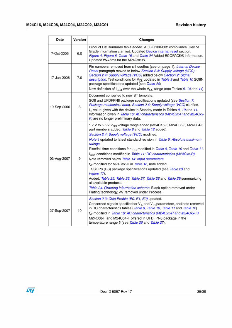
M24C16, M24C08, M24C04, M24C02, M24C01 Revision history
Doc ID 5067 Rev 17 35/38
7-Oct-2005 6.0
Product List summary table added. AEC-Q100-002 compliance. Device Grade information clarified. Updated Device internal reset section, Figure 4, Figure 5, Table 16 and Table 24 Added ECOPACK® information. Updated tW=5ms for the M24Cxx-W.
17-Jan-2006 7.0
Pin numbers removed from silhouettes (see on page 1). Internal Device Reset paragraph moved to below Section 2.4: Supply voltage (VCC). Section 2.4: Supply voltage (VCC) added below Section 2: Signal description. Test conditions for VOL updated in Table 9 and Table 10 SO8N package specifications updated (see Table 20)New definition of ICC1 over the whole VCC range (see Tables 9, 10 and 11).
19-Sep-2006 8
Document converted to new ST template.SO8 and UFDFPN8 package specifications updated (see Section 7: Package mechanical data). Section 2.4: Supply voltage (VCC) clarified. ILI value given with the device in Standby mode in Tables 9, 10 and 11. Information given in Table 16: AC characteristics (M24Cxx-R and M24Cxx-F) are no longer preliminary data.
03-Aug-2007 9
1.7 V to 5.5 V VCC voltage range added (M24C16-F, M24C08-F, M24C04-F part numbers added; Table 8 and Table 12 added).
Section 2.4: Supply voltage (VCC) modified.Note 1 updated to latest standard revision in Table 5: Absolute maximum ratings.Rise/fall time conditions for ICC modified in Table 9, Table 10 and Table 11.
ICC1 conditions modified in Table 11: DC characteristics (M24Cxx-R).
Note removed below Table 14: Input parameters.tW modified for M24Cxx-R in Table 16, note added.
TSSOP8 (DS) package specifications updated (see Table 23 and Figure 17).
Added: Table 25, Table 26, Table 27, Table 28 and Table 29 summarizing all available products.
Table 24: Ordering information scheme: Blank option removed under Plating technology, /W removed under Process.
27-Sep-2007 10
Section 2.3: Chip Enable (E0, E1, E2) updated.Concerned signals specified for VIL and VIH parameters, and note removed in DC characteristics tables (Table 9, Table 10, Table 11 and Table 12).tW modified in Table 16: AC characteristics (M24Cxx-R and M24Cxx-F).
M24C08-F and M24C04-F offered in UFDFPN8 package in the temperature range 5 (see Table 26 and Table 27).
Date Version Changes
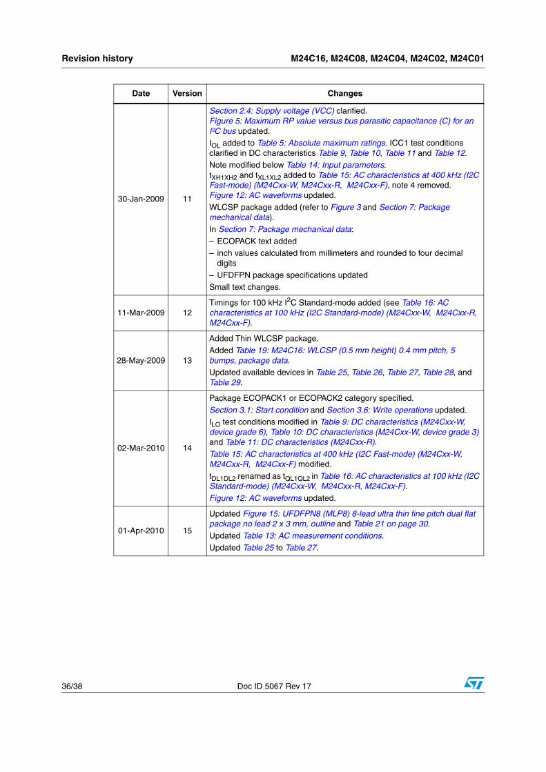
Revision history M24C16, M24C08, M24C04, M24C02, M24C01
36/38 Doc ID 5067 Rev 17
30-Jan-2009 11
Section 2.4: Supply voltage (VCC) clarified. Figure 5: Maximum RP value versus bus parasitic capacitance (C) for an I²C bus updated.IOL added to Table 5: Absolute maximum ratings. ICC1 test conditions clarified in DC characteristics Table 9, Table 10, Table 11 and Table 12.Note modified below Table 14: Input parameters. tXH1XH2 and tXL1XL2 added to Table 15: AC characteristics at 400 kHz (I2C Fast-mode) (M24Cxx-W, M24Cxx-R, M24Cxx-F), note 4 removed. Figure 12: AC waveforms updated.
WLCSP package added (refer to Figure 3 and Section 7: Package mechanical data).
In Section 7: Package mechanical data:
– ECOPACK text added– inch values calculated from millimeters and rounded to four decimal
digits– UFDFPN package specifications updated
Small text changes.
11-Mar-2009 12Timings for 100 kHz I2C Standard-mode added (see Table 16: AC characteristics at 100 kHz (I2C Standard-mode) (M24Cxx-W, M24Cxx-R, M24Cxx-F).
28-May-2009 13
Added Thin WLCSP package.Added Table 19: M24C16: WLCSP (0.5 mm height) 0.4 mm pitch, 5 bumps, package data.Updated available devices in Table 25, Table 26, Table 27, Table 28, and Table 29.
02-Mar-2010 14
Package ECOPACK1 or ECOPACK2 category specified.
Section 3.1: Start condition and Section 3.6: Write operations updated.ILO test conditions modified in Table 9: DC characteristics (M24Cxx-W, device grade 6), Table 10: DC characteristics (M24Cxx-W, device grade 3) and Table 11: DC characteristics (M24Cxx-R).
Table 15: AC characteristics at 400 kHz (I2C Fast-mode) (M24Cxx-W, M24Cxx-R, M24Cxx-F) modified.
tDL1DL2 renamed as tQL1QL2 in Table 16: AC characteristics at 100 kHz (I2C Standard-mode) (M24Cxx-W, M24Cxx-R, M24Cxx-F).
Figure 12: AC waveforms updated.
01-Apr-2010 15
Updated Figure 15: UFDFPN8 (MLP8) 8-lead ultra thin fine pitch dual flat package no lead 2 x 3 mm, outline and Table 21 on page 30.
Updated Table 13: AC measurement conditions.
Updated Table 25 to Table 27.
Date Version Changes
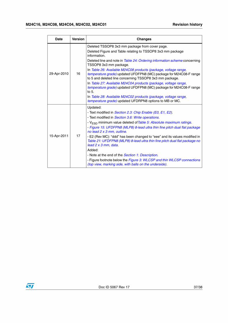
M24C16, M24C08, M24C04, M24C02, M24C01 Revision history
Doc ID 5067 Rev 17 37/38
29-Apr-2010 16
Deleted TSSOP8 3x3 mm package from cover page.
Deleted Figure and Table relating to TSSOP8 3x3 mm package information.
Deleted line and note in Table 24: Ordering information scheme concerning TSSOP8 3x3 mm package.
In Table 26: Available M24C08 products (package, voltage range, temperature grade) updated UFDFPN8 (MC) package for M24C08-F range to 5 and deleted line concerning TSSOP8 3x3 mm package.
In Table 27: Available M24C04 products (package, voltage range, temperature grade) updated UFDFPN8 (MC) package for M24C08-F range to 5.In Table 28: Available M24C02 products (package, voltage range, temperature grade) updated UFDRPN8 options to MB or MC.
15-Apr-2011 17
Updated:
- Text modified in Section 2.3: Chip Enable (E0, E1, E2).
- Text modified in Section 3.6: Write operations.- VESD minimum value deleted ofTable 5: Absolute maximum ratings.
- Figure 15: UFDFPN8 (MLP8) 8-lead ultra thin fine pitch dual flat package no lead 2 x 3 mm, outline.
- E2 (Rev MC): “ddd” has been changed to “eee” and its values modified in Table 21: UFDFPN8 (MLP8) 8-lead ultra thin fine pitch dual flat package no lead 2 x 3 mm, data.Added:
- Note at the end of the Section 1: Description.
- Figure footnote below the Figure 3: WLCSP and thin WLCSP connections (top view, marking side, with balls on the underside).
Date Version Changes
M24C16, M24C08, M24C04, M24C02, M24C01
38/38 Doc ID 5067 Rev 17
Please Read Carefully:
Information in this document is provided solely in connection with ST products. STMicroelectronics NV and its subsidiaries (“ST”) reserve the right to make changes, corrections, modifications or improvements, to this document, and the products and services described herein at any time, without notice.
All ST products are sold pursuant to ST’s terms and conditions of sale.
Purchasers are solely responsible for the choice, selection and use of the ST products and services described herein, and ST assumes no liability whatsoever relating to the choice, selection or use of the ST products and services described herein.
No license, express or implied, by estoppel or otherwise, to any intellectual property rights is granted under this document. If any part of this document refers to any third party products or services it shall not be deemed a license grant by ST for the use of such third party products or services, or any intellectual property contained therein or considered as a warranty covering the use in any manner whatsoever of such third party products or services or any intellectual property contained therein.
UNLESS OTHERWISE SET FORTH IN ST’S TERMS AND CONDITIONS OF SALE ST DISCLAIMS ANY EXPRESS OR IMPLIED WARRANTY WITH RESPECT TO THE USE AND/OR SALE OF ST PRODUCTS INCLUDING WITHOUT LIMITATION IMPLIED WARRANTIES OF MERCHANTABILITY, FITNESS FOR A PARTICULAR PURPOSE (AND THEIR EQUIVALENTS UNDER THE LAWS OF ANY JURISDICTION), OR INFRINGEMENT OF ANY PATENT, COPYRIGHT OR OTHER INTELLECTUAL PROPERTY RIGHT.
UNLESS EXPRESSLY APPROVED IN WRITING BY AN AUTHORIZED ST REPRESENTATIVE, ST PRODUCTS ARE NOT RECOMMENDED, AUTHORIZED OR WARRANTED FOR USE IN MILITARY, AIR CRAFT, SPACE, LIFE SAVING, OR LIFE SUSTAINING APPLICATIONS, NOR IN PRODUCTS OR SYSTEMS WHERE FAILURE OR MALFUNCTION MAY RESULT IN PERSONAL INJURY, DEATH, OR SEVERE PROPERTY OR ENVIRONMENTAL DAMAGE. ST PRODUCTS WHICH ARE NOT SPECIFIED AS "AUTOMOTIVE GRADE" MAY ONLY BE USED IN AUTOMOTIVE APPLICATIONS AT USER’S OWN RISK.
Resale of ST products with provisions different from the statements and/or technical features set forth in this document shall immediately void any warranty granted by ST for the ST product or service described herein and shall not create or extend in any manner whatsoever, any liability of ST.
ST and the ST logo are trademarks or registered trademarks of ST in various countries.
Information in this document supersedes and replaces all information previously supplied.
The ST logo is a registered trademark of STMicroelectronics. All other names are the property of their respective owners.
© 2011 STMicroelectronics - All rights reserved
STMicroelectronics group of companies
Australia - Belgium - Brazil - Canada - China - Czech Republic - Finland - France - Germany - Hong Kong - India - Israel - Italy - Japan - Malaysia - Malta - Morocco - Philippines - Singapore - Spain - Sweden - Switzerland - United Kingdom - United States of America
www.st.com
PCN MMS-MMY/13/7714 - Dated 18 Feb 2013
Please Read Carefully:
Information in this document is provided solely in connection with ST products. STMicroelectronics NV and its subsidiaries(‘‘ST’’) reserve theright to make changes, corrections, modifications or improvements, to this document, and the products and services described herein at anytime, without notice.
All ST products are sold pursuant to ST’s terms and conditions of sale.
Purchasers are solely responsible for the choice, selection and use of the ST products and services described herein, and ST assumes noliability whatsoever relating to the choice, selection or use of the ST products and services described herein.
No license, express or implied, by estoppel or otherwise, to any intellectual property rights is granted under this document. If any part of thisdocument refers to any third party products or services it shall not be deemed a license grant by ST for the use of such third party productsor services, or any intellectual property contained therein or considered as a warranty covering the use in any manner whatsoever of suchthird party products or services or any intellectual property contained therein.
UNLESS OTHERWISE SET FORTH IN ST’S TERMS AND CONDITIONS OF SALE ST DISCLAIMS ANY EXPRESS OR IMPLIEDWARRANTY WITH RESPECT TO THE USE AND / OR SALE OF ST PRODUCTS INCLUDING WITHOUT LIMITATION IMPLIEDWARRANTIES OF MERCHANTABILITY, FITNESS FOR A PARTICULAR PURPOSE ( AND THEIR EQUIVALENTS UNDER THE LAWSOF ANY JURISDICTION ), OR INFRINGEMENT OF ANY PATENT, COPYRIGHT OR OTHER INTELLECTUAL PROPERTY RIGHT.
UNLESS EXPRESSLY APPROVED IN WRITING BY TWO AUTHORIZED ST REPRESENTATIVES, ST PRODUCTS ARE NOTRECOMMENDED, AUTHORIZED OR WARRANTED FOR USE IN MILITARY, AIR CRAFT, SPACE, LIFE SAVING, OR LIFE SUSTAININGAPPLICATIONS, NOR IN PRODUCTS OR SYSTEMS WHERE FAILURE OR MALFUNCTION MAY RESULT IN PERSONAL INJURY,DEATH, OR SEVERE PROPERTY OR ENVIRONMENTAL DAMAGE. ST PRODUCTS WHICH ARE NOT SPECIFIED AS ‘‘AUTOMOTIVEGRADE’’ MAY ONLY BE USED IN AUTOMOTIVE APPLICATIONS AT USER’S OWN RISK.
Resale of ST products with provisions different from the statements and/or technical features set forth in this document shall immediately voidany warranty granted by ST for the ST product or service described herein and shall not create or extend in any manner whatsoever, anyliability of ST.
ST and the ST logo are trademarks or registered trademarks of ST in various countries.
Information in this document supersedes and replaces all information previously supplied.
The ST logo is a registered trademark of STMicroelectronics. All other names are the property of their respective owners
c 2013 STMicroelectronics - All rights reserved.
STMicroelectronics group of companies
Australia - Belgium - Brazil - Canada - China - Czech Republic - Finland - France - Germany - Hong Kong - India - Israel - Italy - Japan -
Malaysia - Malta - Morocco - Philippines - Singapore - Spain - Sweden - Switzerland - United Kingdom - United States of America
www.st.com
® 77/77
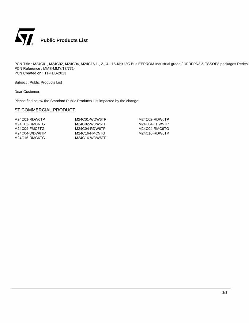
Public Products List®
PCN Title : M24C01, M24C02, M24C04, M24C16 1-, 2-, 4-, 16-Kbit I2C Bus EEPROM Industrial grade / UFDFPN8 & TSSOP8 packages RedesigPCN Reference : MMS-MMY/13/7714 PCN Created on : 11-FEB-2013
Subject : Public Products List
Dear Customer,
Please find below the Standard Public Products List impacted by the change:
ST COMMERCIAL PRODUCT
M24C01-RDW6TP M24C01-WDW6TP M24C02-RDW6TP M24C02-RMC6TG M24C02-WDW6TP M24C04-FDW5TP M24C04-FMC5TG M24C04-RDW6TP M24C04-RMC6TG M24C04-WDW6TP M24C16-FMC5TG M24C16-RDW6TP M24C16-RMC6TG M24C16-WDW6TP
1/1


![Medical Face Mask (Non-Sterile) · 9 User Guide [For Epidemic Use] Product Name: Disposable Medical Face Mask (Non-sterile) Specifications: Flat fold, ear loop,17cm×10cm Model no.:RK-MMY-50](https://img.pdfslide.us/doc/110x75/6025516606ecf37ec90e0c63/medical-face-mask-non-sterile-9-user-guide-for-epidemic-use-product-name-disposable.jpg)