Embed Size (px)
Citation preview

PROCESSNEWS 1
We’ve been lucky that distinguished experts in each field have presented at these webinars. They are available to view again, just look inside this newsletter to find out more about them.
www.oxford-instruments.com/plasma-videos
Data storage, Atomic Layer Deposition, MEMS, Graphene and 2D materials have all been presented recently through our series of webinars
Welcome to this issue of PROCESSNEWS 2 Flexible high performance Silicon-
based inorganic electronics
3 Watch again - Fascinating technical webinars – key expert guest speakers
4/5 Exploring Flatlands at Oxford Instruments
6/7 Atomic layer deposition of dielectric materials
8/9 The application of Bosch™ Deep Silicon Etch (DSiE) to the manufacture of X-Ray lenses
10 ICP plasma etching of tapered Via in Silicon for MEMS integration
11 Metallic nanoparticle formation by sputtering and annealing
12 2D plenary sessions attracted enormous interest at recent Beijing Nanotechnology Seminar
13 Nanoparticle and nanosphere mask for etching of ITO nanostructures and their reflection properties
13 University of Science and Technology of China orders an additional plasma etching system for quantum information processing
14/15 Dust management in silane PECVD systems
16 Introducing our new Service agent in Israel
16 Launching new training dates for 2015
IN THIS ISSUE
PROCESSNEWS 1114A Newsletter from Oxford Instruments Plasma Technology
Follow us on...
/oxinst@oxinst

1114Watch again
Taking nano to the next levelFocusing on recent advances in nanoscale etching and in atomic layer deposition (ALD),
from research to manufacturing applications, this webinar was presented by leaders in their
respective fields of research and production.
Two industry-leading speakers discussed their specialities:
• ALD and nanoscale-etch processing techniques and results from recent work carried out
at the LBNL, Deirdre Olynick, Lawrence Berkeley National Laboratory (LBNL):
• Data storage - a technology area that is benefitting from advances in nanoscale
fabrication, Kim Lee, Seagate
Exploring flatlands: fabrication technologiesOne of the key technical challenges when working towards the commercial realization of
graphene and related 2D materials is the development of robust fabrication techniques for
deposition, etching and integration with other processes in a device-fabrication facility. This
webinar focussed on recent advances in research from academic speakers at the forefront of
their fields, as well as from Oxford Instruments.
What you will gain from this webinar:
• Understanding of the use of controlled etching processes for novel 2D heterostructures
– by Dr Andrey V Kretinin (University of Manchester, UK)
• Growth and characterization of graphene and hexagonal boron nitride via CVD and
plasma-enhanced CVD – by Dr Ravi Sundaram (Oxford Instruments, UK)
• Use of ALD in the deposition of low-resistance contacts and high-k dielectrics on
graphene – by Dr A A Bol (Eindhoven University of Technology, Netherlands)
Fascinating technical webinars – key expert guest speakers
PROCESSNEWS 32 PROCESSNEWS
Galo A. Torres Sevilla and Dr. Muhammad Mustafa Hussain / Integrated Nanotechnology Group, King Abdullah University of Science and Technology (KAUST)
Flexible high performance Silicon-based inorganic electronics
Figure 2 shows a comparison between the performance
of released and unreleased samples. It can be seen that no
degradation is introduced to the devices during peel-off process,
hence making our technique suitable for state of the art devices.
In summary, we have developed and presented a practical
way to transform traditional high performance electronics
into flexible ones without the need of expensive substrates or
processes. We expect that in a close future, this technique may
be used to fabricate high performance wearable and ultra-
portable electronics.
Since the introduction of flexible electronics in 1969, many
different approaches have been demonstrated to create high
performance devices on flexible substrates. The most commonly
known is the use of flexible organic substrates to fabricate
devices using microfabrication processes. However, plastic
semiconductors have many disadvantages when compared with
inorganic ones. Plastic thermal instability together with their
inherited low electron mobility hinder their potential for truly
high performance flexible electronics. For this reason, alternate
approaches have been followed to integrate the electrical
advantages of inorganic substrates with the flexibility of organic
semiconductors. These techniques are usually based on transfer
of silicon nano-ribbons released from costly Si (111) substrates
to plastic host substrates. However, the incompatibility between
transfer techniques and industries’ processes along with the
reduced integration density, hinder their potential for very large
scale integration required for high performance electronics.
For these reasons, in recent years, we have demonstrated state
of the art silicon devices on flexible platforms without the need
of transfer processes or expensive substrates. Our process is
based on etch-release-peel-reuse techniques. First, we fabricate
our devices with state of the art industry compatible processes.
Then, with the aid of BOSCH process (Oxford Instruments
PlasmaPro 100) we etch deep trenches in the passive areas
of the wafer. Depending on the etch depth, the final thickness
of the substrate can be controlled. Next, we protect the lateral
walls of the holes using ALD deposition. Finally, using isotropic
etching of silicon (XeF2), we create caves at the bottom of the
trenches, once these caves meet, the top silicon film can be
easily peeled and flexed due to the extremely reduced thickness
(1 to 20 µm). At this point, the remaining substrate can be
polished and reused making our process industry compatible
and cost effective at the same time.
Figure 1 shows a released sample containing the most advanced
transistor architecture (FinFET). The obtained film is only 1
µm thick exhibiting extremely high flexibility (5 mm minimum
bending radius) and semitransparency due to the etch holes
created for the peeling process.
Figure 1: Released sample containing FinFET transistors. Sample is 1µm thick allowing a minimum bending radius of 5 mm and exhibits semitransparency due to the etch holes introduced during the peel-off process.
Figure 2: Transfer characteristics comparing released and unreleased samples showing no performance degradation due to peel-off process. Gate length (L) = 250nm and width (W) = 3.6 µm.
Contact: [email protected]
Dr Deirdre Olynick, LBNL
Kim Lee, Seagate
Watch either of these webinars at: www.oxford-instruments.com/plasma-videos
Galo A. Torres Sevilla was a guest speaker at our spring seminar at IEMN, Lille, France
Dr Andrey V Kretinin, University of Manchester
Dr Ravi Sundaram, Oxford Instruments
Dr A A Bol, Eindhoven University of Technology

4 PROCESSNEWS PROCESSNEWS 5
Chemical structures are characterized by X-ray photoelectron spectroscopy
(Oxford Instruments-Omicron ESCA+). XPS measurements were performed with
an Al-Kα X-ray source on the samples. Fig. 2 shows the XPS spectrum for the
transferred sample on Nickel, where two peaks at 191.03 eV and 398.4 eV are
identified as the binding energies of the B 1s and N 1s electrons respectively.
These energy values (and integrated intensity analysis) reaffirms the formation
of hexagonal Boron Nitride presented in nearly equal stoichiometric ratio [7].
We have an extensive portfolio of deposition and characterization tools
tailored towards research the field of graphene and 2 dimensional materials.
N 1s
x 103
10
20
30
40
50
60
CP
S
408 404 400 396 392Binding Energy (eV)
B 1s
x 103
4
6
8
10
12
14
16
18
20
22
CP
S
200 196 192 188 184Binding Energy (eV)
References:
[1]. Li, X et al; Science 324, 1312-1314 (2009)
[2] Bae, S. et al; Nat Nanotech. 5, 574 (2010)
[3] Ismach, A. et al; ACS Nano,6, 6378 (2012)
[4] Zhan, Y et al; Small, 8, 966 (2012)
[5] R. Gorbachev et al; Small , 7, 465,(2011)
[6] Reich, S. et al; Phys. Rev. B, 71, 205201, (2005)
[7] Lee, Yi-Hsien et al; RSC Adv., 2, 111(2012)
Fig. 2. (a) Raman spectrum of hBN on Ni showing the characteristic peak ~1368 cm-1 (b)Zoomed in plot of Spectrum shown in (a) to elucidate the absence of non-hBN phase (c) XPS survey scan, (d) N1s(at 398.4 eV) and (e) B1s(at 191.03 eV)
Chemical Vapour Deposition (CVD) has emerged as a
workhorse for the preparation and production of graphene
[1,2] and more recently applied in the synthesis of other
2D materials such as hexagonal Boron Nitride [3] and
Molybdenum Disulphide [4]. We had previously demonstrated
that the Oxford Instruments Nanofab Agile tool with the
capability of both CVD and PECVD processes can be used for
the growth of monolayer graphene and related graphene-like
allotropes. Recently, we have developed a thermal CVD route
to synthesize hexagonal Boron Nitride (hBN) using Nickel foils
as catalyst in this tool.
The processStandard semiconductor process gases, Diborane (B
2H
6) and
Ammonia (NH3) were introduced in the right proportions over
a nickel foil heated (~1000 ºC ) which were pre-treated in
a reducing atmosphere. The reaction of these components
catalysed by nickel resulted in the nucleation and growth of
hBN islands. The load-locked sample transfer enabled quick
sample exchange and also allowed us to precisely arrest the
reaction to observe these growth fronts before the formation
of a continuous film using an SEM and also on an Oxford
Instruments Asylum Research MFP-3D Classic AFM
Dr Ravi Sundaram, Development Scientist, Oxford Instruments
We have been taking a close look at growth and characterisation of 2 dimensional
materials. As the field moves beyond graphene, there is growing interest in
studying atomic planes of other Van der Waals solids and heterostructures
created by stacking layers with complementary characteristics to achieve novel
functionality. One such material that serves as a high quality substrate for
graphene is hexagonal Boron Nitride (hBN).
Fig. 1. (a) SEM image showing a triangular hBN island growing on a Nickel crystal face. (b)AFM topography and (c) AFM lateral force image of a growing edge.
Film characterisationIn order to confirm the deposition of hBN we used Raman spectroscopy and X-Ray Photoelectron Spectroscopy (XPS) (Figure 2).
The presence of a sharp peak at ~1368 cm-1 (excitation at 532 nm) arises from the E2g
phonon and is characteristic of the h-BN
phase. On closer examination of the spectrum we did not see the presence of broad peaks which may arise due to unwanted
co-deposition of the cubic phase, carbon contaminated phase or amorphous BN soot.
1000 1100 1200 1300 1400 1500 1600
0
200
400
600
800
1000
1200
1400
1600
1800
2000
Inte
nsity
(a.u
.)
Raman Shift (cm-1)
Lorentz
Position1367.534 0.11898
FWHM 21.413 0.37
Please contact us for more information on graphene and other 2 dimensional materials:
[email protected] or visit www.oxford-instruments.com/graphene
1114Exploring Flatlands at Oxford Instruments
N1s:398.4 B1s:191.03

0614
PROCESSNEWS 76 PROCESSNEWS
Harm Knoops and Tom Sharp, Oxford Instruments
Atomic layer deposition of dielectric materials
Atomic layer deposition (ALD) is of interest for controlled
deposition of dielectric materials in complex device structures.
To serve the needs of the wide range of devices and applications
fields which can benefit from these dielectric films, there is
a constant drive towards new ALD processes and improved
material properties (e.g., higher dielectric constant). Furthermore
for many applications there is a desire to go towards lower
temperatures, while maintaining high material quality.
To this end, several oxidants can be applied in the ALD cycle
such as water, ozone and oxygen plasma, which differ in
oxidizing strength. Figure 1 shows an overview of common
dielectric materials and whether they have been grown using
Oxford Instrument systems (OpAL and/or FlexAL). The usage
of oxygen plasma allows the deposition of the widest range
of oxides and furthermore has been demonstrated to allow
deposition at room temperature for some (Al2O
3, SiO
2, and
TiO2 have been demonstrated by the Eindhoven University of
Technology). Note that for deposition on sensitive substrates
(such as III-V materials) a low power plasma or weaker oxidant
could be desired.
Besides binary oxides, also the desire to deposit multi-
component oxides using ALD is present. For instance
stoichiometric strontium titanate oxide (STO) can have very
high k values. The cycle wise nature of the ALD process and
the recipe based software of the OpAL and FlexAL allows
easy mixing of materials by alternating ALD cycles of the
binary compounds. Figure 2 for instance shows how the
optical properties of STO deposited on a FlexAL system
can be tuned by varying the [SrO]/[TiO2] ALD cycle ratio. This
example furthermore shows how in situ ellipsometry can be
used to determine the stoichiometry for these materials. Post-
annealing at 600/650 °C for 10 min under N2 gas resulted
in a crystallization into the high-k perovskite phase. The
highest capacitance density has been demonstrated for 15 nm
polycrystalline stoichiometric SrTiO3 films resulting in a capacitor
equivalent thickness (CET) of about 0.7 nm.
One of the main advantages of ALD is its inherent high
conformality, which for instance can be used to deposit
Figure 1 Common dielectric materials and possible oxidants by which they have been deposited. Materials that have been grown at room temperature are also indicated. Processes in blank spaces may have been demonstrated in literature but have not yet been directly demonstrated by Oxford Instruments. Material list is not exhaustive.
dielectric films for trench capacitors. Due to the self-limiting
nature of the ALD surface reactions, complex 3D structures
can be covered with films of equal thickness throughout the
structure, as long as sufficient flux of precursor and oxidant
has reached all surfaces. For thermal ALD processes conformal
coating of extremely high aspect ratio (>1000:1) has been
reported. In this case methods to enclose the precursor in the
reactor chamber, such as the automatic pressure control valve
(APC), are beneficial to limit the precursor usage per cycle
(note that the APC which is standard on the FlexAL system is
now also available as an option for the OpAL system). Due to
recombination of plasma radicals at surfaces, conformality for
plasma processes can be more challenging depending on radical
type and surface material. Nonetheless, conformal coating of
high aspect ratio structures is achievable by plasma deposition.
For instance for plasma ALD of SiO2, conformal coating of 30:1
trenches using an OpAL has been reported. Also for plasma
ALD of HfO2, high conformality can be obtained as shown in
Fig. 3. Here 25:1 trenches are coated by 20 nm HfO2. In general
Oxford Instruments ALD tools are equipped to deposit a wide
range of dielectric materials under demanding conditions, such
as room temperature deposition, stoichiometry control of ultra-
high k materials, and plasma deposition in 3D structures.
Figure 2 (a) Real and imaginary part of the dielectric functions ε1 (a) and ε2 (b), respectively, of as-deposited TiO2, SrO and of STO films.
The corresponding [Sr]/([Sr]+[Ti]) content ratio from RBS and [SrO]/[TiO2] cycle ratio are indicated for the STO films.
Potts et al., Chem. Vap. Deposition, 19, 125 (2013)Aslam et al., Phys. Status Solidi A 211, 389 (2013)Dingemans et al., J. Electrochem. Soc. 159, H277 (2012)Longo et al., ECS Trans. 41, 63 (2011), and ECS J. Solid State Sci. Technol. 2, N15 (2013)
Figure 3 SEM image of Si trenches (AR = 25:1) with conformal coating by plasma ALD of HfO
2 (20 nm) as shown by insets of SEM
images on the right at the trench corner and the trench bottom.
Al2O3 HfO2 SiO2 Ta2O5 TiO2 ZrO2 SrTiO3
Water ✔ ✔ ✗ ✔ ✔ ✔ ✗
Ozone ✔ ✔ ✔
Plasma ✔ ✔ ✔ ✔ ✔ ✔ ✔
Room Temp. ✔ ✔ ✔

8 PROCESSNEWS
1114
PROCESSNEWS 9
Katarzyna Korwin-Mikke a, Mark E McNie a, Lucia Alianelli b
a Oxford Instruments Plasma Technology, Yatton, BS494AP, United Kingdomb STFC Diamond Light Source, Oxfordshire, OX11 0DE, United Kingdom
etched lenses is to tune the process to operate at low pressures
and a low (controllable) DC bias. The other is to reduce the
number of ion impacts on the sidewalls by protecting the lenses
with sacrificial features that can be removed after the process.
In the Oxford Instruments Applications Laboratory, etch
processes for each approach were developed (with and without
compensating features – Fig.2). The results gave close to vertical
lens profiles (89.90°) without compensating features etched to
50µm depth with no mask undercut and controlled scallops to
below 50nm (Fig.3). This process was adapted and extended to
the lenses with compensation features to achieve etch depths in
excess of 70µm with smooth sidewalls (scallops <50nm), no mask
undercut or sidewall damage, vertical profile (89.94°) and clean
surfaces in open silicon areas (Fig.4).
The X-Ray silicon lens etch processes were carried out in a
PlasmaPro 100 Estrelas deep silicon etch tool (Fig.5). This
latest generation deep silicon etch system can trade high rate
performance for increased control to enable a very flexible set
of processes from high etch rate applications (>25µm/min) to
nanoscale etching. The lens processes are being transferred to a
third party commercial supplier for production of the lenses going
forwards.
Adapted from work presented at the International Micro Nano
Engineering (MNE) Conference, Sept. 2014
The trend in X-Ray optical devices, such as refractive lenses, zone plates, curved mirrors, multilayers and multilayer Laue lenses, is towards shrinking dimensions and/or deeper
optics.
Due to excellent properties, such as thermal x-ray absorption, diamond is highly desirable material for use in many optical instruments, however, due to cost of manufacturing, extreme hardness and resistance to chemical attack, diamond is a difficult material to realize structures suitable for x-ray lenses and this is why silicon is the leading material for x-ray lens production. Nanofocusing silicon x-ray lenses require not only high quality material but also high aspect ratio with vertical sidewalls and controlled roughness on the sidewalls to minimize aberrations and parasitic scattering respectively. The focus of this work was to develop the process for etching silicon x-ray lenses with good profile control and smooth sidewalls using the Oxford Instruments PlasmaPro 100 Estrelas etch tool.
To achieve high aspect ratio lenses with vertical profiles and
smooth sidewalls, a short cycle time is used in conjunction
with lower powers for less aggressive process conditions. The
passivation is regularly refreshed to maintain sidewall integrity
through rapid switching with controlled ion energies. Etching
microstructures on the samples with a high silicon exposed area
reduces the etch rate due to loading effects and may cause
undercut of the mask as the result of sidewall plasma attack on
isolated features (Fig.1) even when overpassivated. One of the
solutions to reducing the negative impact of the ions on the
The application of Bosch™ Deep Silicon Etch (DSiE) to the manufacture of x-ray lenses
Figure 1. The negative impact of the ions on etched X-Ray lens structure.
Figure 2. Device mask patterns. Left: Lens with compensation features; Right: Lens without compensation features.
Figure 3. SEM of a lens without compensation features etched to 50µm depth.
Figure 4. SEM of a lens with compensation features etched to 75µm depth. Figure5. PlasmaPro 100 Estrelas.
PROCESSNEWS 11
A proposed method for enhancing the efficiency of silicon solar
cells is to incorporate nanoparticles of gold or aluminium for
improved light capture. In order to develop practical nanoparticle
optimisation criteria, equipment which is suitably scaled for
research, but traceable to volume production is required. To
synthesise nanoparticles, precise and repeatable deposition of thin
metallic films is done using a multiple target magnetron sputtering
tool and post-deposition with an in-situ heater.
Magnetron sputtering is a well established large area technique
for the deposition of metals. In this investigation we have prepared
uniform sputtered films varying in thickness from 200nm to less
than 10nm for nanoparticle seed layers. Deposition rates are
high and result in short sputtering times for the film thickness
required so a cyclical deposition mode is used with short deposition
times and low discharge powers. Resistivity data from multi-
layers formed by successive passes beneath the deposition flux
demonstrates the thickness control that can be met in this mode
which mimics an in-line sputter configuration.
When the substrate is oscillated beneath the target, a shaper is
used to correct the arrival flux such that the sputtered thin films are
uniform and thin. The shaper can be further refined to permit the
use of a range of instantaneous deposition rates which may in turn
influence the morphology of the thin film. When depositing thin
films for short processing times there is a stringent need for process
repeatability. Au film sputtered to date has been 4 nm thick,
determined by measuring the resistivity with a four point probe.
We show examples of nanoparticle formation by post deposition
annealing. These indicate that for successful aluminium
nanoparticle formation, a full in vacuum process is necessary, while
for gold ex-situ annealing may be practical. This is an important
factor in enabling research into the impact of particle size and
distribution to the silicon solar cell efficiency.
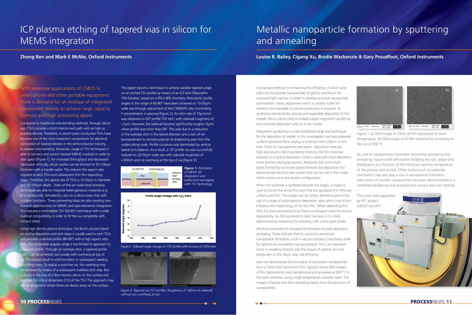
Here we demonstrate the formation of aluminium nanoparticles
from a 10nm thick aluminium film. Figure 6 shows SEM images
of film deposited at room temperature and annealed at 600 °C in
the same chamber, using a high temperature substrate table. The
images of before and after annealing clearly show the presence of
nanoparticles.
Figure 1 (a) SEM image of 10nm Al Film deposited at room
temperature; (b) SEM image of Al NPs obtained by annealing Al
film (a) at 600 °C
Au and Al nanoparticles have been formed by sputtering and
annealing. Future work will involve studying the size, shape and
distribution as a function of film thickness and the temperature
of the process and anneal. Other factors such as substrate
orientation may also play a role in nanoparticle formation.
Fabrication of metallic nanoparticles has been demonstrated in a
combined sputtering and anealing tool using a low-cost method.
This work was supported
by FP7 project
246331nanoPV.
ICP plasma etching of tapered vias in silicon for MEMS integration
Metallic nanoparticle formation by sputtering and annealing
Zhong Ren and Mark E McNie, Oxford Instruments Louise R. Bailey, Cigang Xu, Brodie Mackenzie & Gary Proudfoot, Oxford Instruments
This paper reports a technique to achieve variable tapered angle
on an etched TSV profile by means of an ICP etch (PlasmaPro
100 Estrelas), based on a SF6-C4F8 chemistry. Monotonic profile
angles in the range of 60-80º have been achieved on 10-50µm
wide vias through adjustment of the C4F8/SF6 ratio (controlling
F concentration in plasma) [Figure 2]. An etch rate of 10µm/min
was obtained on 60º profile TSV etch, with sidewall roughness of
<1µm. However, the sidewall became significantly rougher (3µm)
when profile was more than 68º. This was due to a reduction
of the isotropic etch in the lateral direction and a lack of ion
bombardment to remove polymer at shadowing area from the
undercutting mask. Profile curvature was dominated by vertical:
lateral etch balance. As a result, a 72º profile via was successfully
realized on 20-50µm wide vias with sidewall roughness of
<300nm and no overhang at the top of via [Figure 3].
Figure 1. Illustration of MEMS 3D integration and wafer-level packaging with TSV technology
Figure 2. Sidewall angle change on TSV profile with increase of C4F8 ratio
Figure 3. Tapered via (72º profile): Roughness of 180nm on sidewall, without any overhang at top
(a) (b)
10 PROCESSNEWS
With extensive applications of CMOS in
smart phone and other portable equipment
there is demand for an increase of integrated
component density to achieve large capacity
memory and high processing speed.
Compared to traditional wire-bonding methods, through silicon
vias (TSVs) provide a short interconnect path with as high as
possible density. Therefore, in recent years conductive TSVs have
become one of the most important components for electrical
connection of stacked devices in the semiconductor industry,
to replace wire bonding. Moreover, usage of TSV techniques is
able to connect and control stacked MEMS modules in order to
save space [Figure 1]. For increased throughput and decreased
fabrication difficulty, silicon wafers can be thinned to 50-100µm
thickness with a handle wafer. This reduces the aspect ratio
required to etch TSVs and subsequent thin film depositing
steps. Therefore, the typical size of TSVs is 10-50µm in diameter
and 50-100µm depth. State-of-the-art wafer-level bonding
techniques are able to integrate heterogeneous materials (e.g.
III-V compounds, ferroelectric, etc) on a silicon base chip with
multiple functions. These pioneering ideas are also creating new
research opportunities for MEMS and opto-electronic integration.
This requires a controllable TSV (60-85º) technique with a wide
material compatibility, in order to fill the via completely with
contact metal.
Using high density plasma technique, the Bosch process based
on cycling deposition and etch steps is usually used to etch TSVs
and provides a vertical profile (88-90º) with a high aspect ratio
(AR). The achievable angular range is too limited to approach to
a tapered profile. Through an isotropic etch, a tapered profile
(<85º) can be achieved, but usually with overhang at top of
via. This would result in void formation in subsequent seeding
and filling steps. To realize a void-free via, this overhang may
be removed by means of a subsequent maskless etch step. But
it results in the loss of a few microns silicon on the surface and
enlarges the critical dimension (CD) of the TSV. The approach may
not be acceptable where there are device areas on the surface.
12 PROCESSNEWS
An additional Oxford Instruments PlasmaPro 100 plasma
etch system was recently ordered by the Center for Micro
and Nanoscale Research and Fabrication at the University of
Science and Technology of China (USTC) Hefei city, Anhui
Province, adding to their already significant installed base of
our leading etch and deposition systems. The systems are
installed in USTC’s newly opened cleanroom and will be used
for fundamental research into the increasingly important field
of quantum information processing.
Multiple Oxford Instruments plasma systems, including a
PlasmaPro 100 ICP380 and PlasmaPro NGP 80 RIE, and
PlasmaPro 100 PECVD deposition tools were already installed
in USTC’s new facility during the past year.
“Our latest Oxford Instruments plasma etching system will
enhance the cutting edge research capabilities in Quantum
Information Processing, currently being undertaken at our
excellent new facility.” Said Prof Zhu, from USTC, “We chose
Oxford Instruments systems as we have found that they offer
extensive process capabilities, and great flexibility, backed by
excellent support and service packages. These tools will allow
our researchers to push the limits in micro- and nanoscale
fundamental research.”
Prof Zhu continued, “USTC has a very strong background in
both nanoscale science and engineering, and this new state-
of-the-art nanofabrication facility aims to drive collaborative,
interdisciplinary, and fundamental research in the micro- and
nano-scale.”
University of Science and Technology of China orders an additional plasma etching system for quantum information processing
2D plenary sessions attracted enormous interest at recent Beijing Nanotechnology Seminar
Nanoparticle and nanosphere mask for etching of ITO nanostructures and their reflection propertiesCigang Xu*1, Ligang Deng1, Adam Holder1, Louise R. Bailey1,
Caspar Leendertz2, Joachim Bergmann3, Gary Proudfoot1,
Owain Thomas1, Robert Gunn1
Au nanoparticles and polystyrene nanospheres were used as
a mask for plasma etching of an indium tin oxide (ITO) layer.
By reactive ion etching (RIE) processes, the morphology of
polystyrene nanospheres can be tuned through chemical or
physical etching, and an Au nanoparticle mask can result in
ITO nanostructures with larger aspect ratio than a nanosphere
mask. During inductively coupled plasma (ICP) processes, Au
nanoparticle mask was not affected by the thermal effect of
plasma, whereas temperature of the substrate was essential to
protect nanospheres from the damaging effect of plasma.
Physical bombardment in the plasma can also modify the
nanospheres. It was observed that under the same process
conditions, the ratio of CH4 and H
2 in the process gas can
affect the etching rate of ITO without completely etching the
nanospheres. The morphology of ITO nanostructures also
depends on process conditions. The resulting ITO nanostructures
show lower reflection in a spectral range of 400–1000nm than
c-Si and conventional antireflection layer of SiNx film.
ITO nanostructures obtained after etching (scale bar = 200 nm)
1 Oxford Instruments Plasma Technology, North End Road, Yatton, Bristol BS49 4AP, UK
2 Helmholtz-Zentrum Berlin für Materialien und Energie, Institut für Silizium Photovoltaik, Kekuléstr. 5, 12489 Berlin, Germany
3 Leibniz Institute of Photonic Technology, Albert-Einstein-Str. 9, 07745 Jena, Germany
The full article appeared in PSSA Journal DOI:10.1002/pssa.201431228(2014)
PROCESSNEWS 13
To find out about our forthcoming seminars:
www.oxford-instruments.com
Leading high level international speakers
dominated the Oxford Instruments two day
technical seminar hosted at the prestigious Institute
of Physics in Beijing recently. This event focused
on practical applications, techniques and advances
during a half day ‘2D materials’ plenary session,
and many other applications areas.
Expert speakers from key establishments in China, Europe and
the USA gave talks, as did Oxford Instruments specialists, keeping
participants abreast of the latest technologies and trends in many
current and future industry research topics, including:
• Recent Advancements in 2D Materials at Manchester,
Dr. Aravind Vijayaraghavan, National Graphene Institute in Manchester, UK
• ALD applications for power semi and advanced materials
Prof. Erwin Kessels, Tue Eindhoven, NL
• Nanoscale Terahertz Imaging and Spectroscopy of 2D Materials,
Prof. Yukio Kawano, Quantum Nanoelectronics Research Center, Tokyo Institute of Technology, Japan
• Superconductors and Spin-Based Quantum Processors
Prof. David Cory, University of Waterloo, Canada
• Exchange Induced Interfacial Field from Magnetic Insulators
Prof. Guoxing MIAO, Institute for Quantum Computing, University of Waterloo, Canada
• TEM studies of Nano Core/Shell Hetero structures EDS mapping
at the atomic level
Prof. Robert Klie, University of Illinois Chicago
• Fabrication of dielectric coatings using Optofab3000 Ion Beam
sputtering deposition system
Dr. Xiaodong WANG, Institute of Semiconductors, CAS
• Structure and properties of graphene and graphene-like 2D
materials by STM
Prof. Yeliang WANG, Institute of Physics, CAS
• Nano-structure fabrication by ICP-RIE for optical devices
Dr. Zhe LIU, Institute of Physics, CAS
It was great to host such high calibre speakers and attendance at
the IOP. This event showcased the breadth and diversity of Oxford
Instruments tools and applications, and also it offered a good
opportunity for the wider Nanotechnology research and fabrication
community to meet and share their experiences and vision for the
future of this exciting area.

14 PROCESSNEWS PROCESSNEWS 15
1114Use of atomic layer deposition for MEMS & NEMS applications
Watch again
Webinar hosted by the MEMS Industry Group
Atomic layer deposition (ALD) with its growth control
and unique properties can be used to grow an increasing
variety of films in complex structures. As MEMS and
NEMS applications are becoming more advanced, this
webinar discussed important aspects of ALD and how
they can be applied to MEMS.
Mechanical properties that are important for MEMS, such
as stress, were discussed for thermal and plasma ALD.
Several examples from the literature of how ALD films
can be used in MEMS applications were demonstrated
and discussed.
Presented by Oxford
Instruments’ ALD Technical
Sales Specialist Dr. Harm
Knoops. Before his current
position, Harm investigated the
fundamentals and applications
of atomic layer deposition (ALD)
at the Eindhoven University of
Technology.
Dust management in silane PECVD systems
Dr Mike Cooke, CTO, Oxford Instruments Plasma Technology
Dust creation in plasma enhanced chemical vapour deposition
(PECVD) tools can affect user safety, system reliability, and process
quality. There are two main issues:
- Upstream dust creation, from homogeneous gas reactions in
mixtures of silane and oxidising gases. This can add particles to
wafers, and in the worst case block a gas entry line.
- Downstream dust accumulation of partially reacted silane.
This rarely affects process quality, but can be a serious safety
concern.
Both are made worse the more intensively the tool is used, and the
higher quantity of silane used. We have seen a steady increase in
the total silane flow in PECVD processes, as higher rate processes
are introduced. ICPCVD processes are also becoming more widely
used, and such processes normally use 100% silane.
Regrettably, there have been very serious silane incidents across
the semiconductor industry, almost all involving the silane gas
cylinder or gas delivery. PECVD processes themselves have been in
regular, safe use for decades. This article is not concerned with safe
delivery of silane to the gas box, nor with management of effluent out of
the tool, but only with good practice in managing the PECVD tool.
Upstream powderOxford Instruments assesses the likelihood of upstream powder formation
when a tool is ordered or upgraded. We strongly recommend that
changes to the gases used or increases in maximum flow rates are only
done in consultation with Oxford Instruments. For example, we may
recommend splitting the gas manifold, so that gases mix closer to the
process chamber, or adding upstream pressure monitoring devices to
alert the user to potential line blockages.
Silane reacts far more readily with oxygen than with nitrous oxide, so
we recommend avoiding having oxygen and silane in the same gas box
where possible. We have developed and recommend plasma cleaning
processes using CF4 and N
2O rather than the CF
4/O
2 mixture used
historically.
Good practiceWhere oxygen and silane share some common pipe work, but are
not used together:
• Flush the line, preferably with an inert gas, between silane and
oxygen use
• At least 5 minutes, at least 100 sccm flow
• Pump the line thoroughly before first use of silane and before
first use of oxygen
• At least 20 minutes pumping for a gas box up to 5 metres
from the chamber
• Venting. Use the same procedure before and after venting a
chamber, to prevent air and silane meeting.
The same advice applies to gas delivery lines both to downstream
injection points in ICPCVD (‘gas rings’) and to PECVD showerhead
entry points.
DiagnosticsThe wafer is a good indicator that powder is forming upstream,
because it is often visible to the naked eye. Inspect the wafer under a
bright light for signs of roughness, especially in a pattern matching the
showerhead holes. Such powder might be formed at the showerhead
itself, and eliminated by process changes or by renewing the showerhead.
Issue Worst case fault
Mitigations
Silane – oxidiser reaction up-stream
Worse for silicon dioxide PECVD
Gas line blocks
Mix silane and oxidiser at the lowest possible pressure, close to the process chamber
Use N2O oxidiser not oxygen
Use dilute silane, not 100% silane
Perform regular checks for signs of lines blocking
Investigate if there is an increase in particles on the wafer
Pump and purge lines between gas box and chamber thoroughly before venting
Partially reacted powder downstream, building up in the vacuum line to the pump
Worse for amorphous silicon or silicon nitride PECVD
Dust explosion
Perform regular plasma cleaning
Inspect vacuum line regularly
Run a test wafer and a high flow (>500sccm) of gas and no plasma
to detect if powder is blowing down the line. Irregular mass flow
controller (MFC) behaviour, such as long stabilisation time or
failure to achieve higher flow, could be an indication of powder.
(Inadequate upstream pressure or a faulty MFC should also be
considered).
If a line is contaminated, repeated partial venting with inert gas and
pumping out can sometimes clear powder. Heavy contamination
might need partial disassembly and blowing through to clear
powder, or even renewal of pipe sections.
Downstream powderThis problem is rare, but is also less well known. Type ‘dust explosion’
into a search engine if you are unfamiliar with the issue. White
downstream dust from silicon dioxide PECVD is only a problem to
mechanical components (pumps and valves) and rarely travels back
to the process chamber unless a vacuum joint is opened without first
venting the chamber..
Orange or red dusts in exhaust lines of PECVD tools used for
silicon nitride or amorphous silicon deposition are potentially
hazardous, as well as giving rise to mechanical troubles. If such
powder builds up to more than a millimetre or so, then it can be
dislodged and create a dust cloud in the pipe. If this happens when
pumping down a chamber full of air, the conditions are satisfied for
a dust explosion. A bulletin highlighting this hazard has been written
and is available on request. Contact [email protected]
Good practicePlasma clean the chamber as recommended by Oxford Instruments.
This will help to oxidise downstream dust, as well as clean the
process chamber. Inspect the vacuum line regularly. Make the first
inspection after 3 months use, then adjust the interval based on the
amount and type of dust seen. Avoid building up more than 1mm
thickness of dust on the pipe wall.
As with all safety matters which depend on how the tool is used, it is
the user’s responsibility to ensure safe operation - Oxford Instruments
are not safety consultants, but will share our own best practice with
our customers.
To view this webinar:
www.oxford-instruments.com/aldformems

16 PROCESSNEWS
We recently signed an agreement with Asher Sonego to provide comprehensive service support to our customers in Israel.
Asher just finished an intensive training course at Oxford Instruments Plasma Technology’s UK manufacturing facility.
“I am extremely impressed by Oxford Instruments leading edge products and commitment to their customers, to provide the very best tools and world-class service and support”, said Asher, “I am excited to be a part of the team and represent the company in Israel.”
Our courses are designed to improve system maintenance and process techniques for engineers and technicians. We ensure our customers get the most from their Oxford Instruments system.
Benefits
• Courses are run by our dedicated training officer supported by our experienced process and system engineers, who know the systems and understand your individual requirements
• We aim to provide the very best training, tailored to meet with your individual needs
• We limit numbers on each course, to ensure best training possible
Book early to ensure your place for 2015 trainingFor more information: www.oxford-instruments.com/trainingEmail: [email protected]
www.oxford-instruments.com/plasma for more information or scan the code...
This publication is the copyright of Oxford Instruments plc and provides outline information only, which (unless agreed by the company in writing) may not be used, applied or reproduced for any purpose or form part of any order or contract or regarded as the representation relating to the products or services concerned. Oxford Instruments’ policy is one of continued improvement. The company reserves the right to alter, without notice the specification, design or conditions of supply of any product or service. Oxford Instruments acknowledges all trademarks and registrations. © Oxford Instruments plc, 2014. All rights reserved. Ref: OIPT/ProcessNews/2014/02
Oxford Instruments Plasma Technology
For more information please email: [email protected]
UKYattonTel: +44 (0) 1934 837000
GermanyWiesbadenTel: +49 (0) 6122 937 161
India MumbaiTel: +91 22 4253 5100
JapanTokyoTel: +81 3 5245 3261
PR ChinaShanghaiTel: +86 21 6132 9688
BeijingTel: +86 10 6518 8160/1/2
SingaporeTel: +65 6337 6848
TaiwanTel: +886 3 5788696
US, Canada & Latin AmericaConcord, MATOLLFREE: +1 800 447 4717
www.oxford-instruments.com
Oxford Instruments Plasma Technology focuses for the future
Introducing our new service agent in Israel
Launching new training dates for 2015
Mike Smyth, EMEA BusinessManager, Oxford InstrumentsPlasma Technology and Asher Sonego, shake hands while exchanging the signed Agency agreement
![CB,HBI,HBN目錄 2019.02.27 (宏聯)¼CBI/HBI/HBN... · 4 - - Nominal flow rate [m³/h] 3 0 HQBE (HBI ) HQQE (HBN ) Number of stages x10 Mechanical Seals HBI (N) 8 , 12 8 - 1](https://img.pdfslide.us/doc/110x75/5f06dfae7e708231d41a29ed/cbhbihbnceoe-20190227-e-cbiihbiihbn-4-nominal-flow-rate.jpg)