Embed Size (px)
Citation preview
Probe field enhancement in photonic crystals by upconversionnanoparticles
Jingyu Zhang,a) Teresa E. Pick, Daniel Gargas, Scott Dhuey, Emory M. Chan, Ying Wu,Xiaogan Liang, P. James Schuck, Deirdre L. Olynick, Brett A. Helms, and Stefano Cabrinib)
Molecular Foundry, Lawrence Berkeley National Laboratory, 1 Cyclotron Rd, Berkeley,California 94720
(Received 27 July 2011; accepted 26 October 2011; published 18 November 2011)
Lanthanide-doped upconverting nanoparticles, converting low frequency light to high frequency
light through a multiphoton process, have shown interesting properties for bioimaging. Here, the
authors describe a method to deposit a thin layer of upconverting Er3þ doped NaYF4 nanoparticles
(15 to 25-nm) on a quasi-zero-average-index crystal over a 2� 4 mm area to observe light propagation
through the structure. Assisted by the photoluminescence of the nanoparticles with upconverting
three-photon process, the enhanced field intensity confined in photonic crystals at near infrared
wavelength is detected in visible green light under conventional optical microscope. This new
technique has distinct advantages over the typical near infrared setups with infrared camera or
near-field scanning optical microscope setups. VC 2011 American Vacuum Society.
[DOI: 10.1116/1.3662086]
I. INTRODUCTION AND MOTIVATION
Photonic crystals have the ability to confine and mani-
pulate light and are playing a major role in the rapid devel-
opment of today’s information and communication
technology.1,2 Here, we propose a new technique to map
propagation and confinement of near infrared (NIR) light in
photonic crystals (PC) based on the use of upconverting
nanoparticles (UCNPs). Er3þ doped NaYF4 nanoparticles
deposited on the open surface of the PC convert 1.55 lm
light to visible wavelengths through multiphoton absorption
based on sequential energy transfers involving real
metastable-excited states.3,4 This new technique has distinct
advantages over the typical NIR setups composed by micro-
nanostage and IR camera5,6 with resolution limitation due to
the NIR wavelength, or near-field scanning optical micro-
scope setups which are limited by extremely shallow depth
of field and long scanning times. The upconversion method
has a three-fold increase in resolution due to detection of
green instead of IR wavelengths. The upconversion lumines-
cence (UCL) of the 550 nm Er3þ:4S3=2!4I15=2 transition
monotonically increases with increasing fluences (at NIR)
for a very large range of intensity. The photoluminescence
(PL) intensity reflects the relative strength of local field in-
tensity on PC. When the input intensity is low (<1 W=cm2),
the three-photon process for emission of visible light is pro-
portional to the cube of the 1.55 lm excitation intensity
(IPL / I3x).7–9 The PL image is much sharper than the corre-
sponding IR image at low input intensity for a Gaussian laser
beam distribution. At a higher intensity (�500 W=cm2), the
UCL in the visible spectrum is close to a linear response of
the input NIR intensity (IPL ! Ix) due to the saturation
effects in the intermediate energy states,9 allowing UCL to
remain effective for imaging field enhancement detection at
high fluences. The intensity of the PL at one visible wave-
length (550 nm) is the unit area of PL power integrated
with all nanoparticles. Therefore, to extract precise NIR field
strengths from upconversion intensity maps, the upconvert-
ing nanoparticles must be deposited uniformly in the pho-
tonic crystals over a very large area. In this paper, we
present a facile approach to deposit a uniform, thin layer of
nanoparticles on PC surfaces over large areas, enabling the
detection of localized electrical field intensity differences
with optical microscopy.
Previously, we introduced a quasi-zero-average-index
(QZAI) photonic crystals composed of negative index
(n¼�1) PC and positive index (n¼1) air in periodic arrays.5
This structure allows focusing of 1.55 lm wavelength light
in a Si waveguide under transverse mode (TM) polarized ex-
citation. This structure will be exploited and deposited by
UCNPs for image testing. We discuss high aspect ratio Si
PC fabrication, nanoparticle synthesis and the deposition of
a thin layer of nanoparticles over the large area PC surface.
The nanoparticle deposition process was optimized for high
uniformity as a key for signal interpretation. The schematic
of fabrication flows has been shown in Fig. 1. Via these
films, we detect the 550 nm PL signal emitted from the nano-
particles which arises due to the upconversion of the propa-
gating NIR field intensity in the PC.
II. PHOTONIC CRYSTALS FABRICATION
We fabricate a 2� 4 mm structure composed of negative
index (n¼�1) PC on silicon and positive index (n¼1) air
slabs, arranged in a periodic 1D array. A 1.55 lm wave-
length light with TM polarization, entering parallel to the
plane of the silicon surface and perpendicular to the length
of the stripe, is focused by the PC and the air stripe due to
light bending at the interface of positive and negative index
structures. In the previous work,5 the PC structure was
etched into silicon using a gas chopping plasma etching pro-
cess which alternates an etching step using SF6, Ar with a
passivation step using CHF3 and CH4. One cycle consists of
a)Electronic mail: [email protected])Electronic mail: [email protected]
06F403-1 J. Vac. Sci. Technol. B 29(6), Nov/Dec 2011 1071-1023/2011/29(6)/06F403/5/$30.00 VC 2011 American Vacuum Society 06F403-1
one step of etching and passivation and the overall process
requires hundreds of cycles for the deep etching (�1.5 to
2 lm) of the high aspect ratio features (�10) which compose
the PC. There are several disadvantages for gas chopping
plasma etching. In our system, the overhead required to
switch between the steps make the etching process slow. The
etch rates are �1 lm=hour. In addition, the process causes
major serious chamber contamination due to passivant depo-
sition throughout the chamber. Finally, the alternating
step process results in a characteristic sidewall ripple of
10–100 nm. The roughness can increase the loss for photonic
devices.10 Here we optimize an improved etching process
which uses SF6=O2 plasma chemistry at cryogenic wafer
temperatures.11,12 Starting with a silicon-on-insulator (SOI)
wafer (1.5 lm silicon layer on top of 1 lm oxide layer), we
spin on ZEP 520, a positive electron beam (EB) resist at a
thickness of 370 nm. The resist is patterned using a Vistec
VB300UHR EWF electron-beam lithography (EBL) System,
and developed with n-amyl acetate. The EB patterned resist
is used as a mask to etch the underlying silicon layer, down
to the SOI, in an Oxford Plasmalab 100 ICP=RIE with resist
mask. The SF6 chemistry provides the free radicals for iso-
tropic Si etching, while O2 promotes the growth (at cryo-
genic temperatures) of a passivation film. This passivation
film, with a generic temperature sensitive formula SixFyOz,
protects the side walls of the etched structures and disappears
after warming to room temperature leaving behind a clean
surface.13,14 Here, the etching was performed at �120 �C. The
etch program steps include 1) wafer cool down (2 min), 2)
plasma strike (RF power 100 W, ICP power 700 W, SF6 42
sccm and O2 15 sccm, 7 mTorr chamber pressure, 3 sec); 3)
O2 passivation (RF power 100 W, ICP power 700 W, SF6
42 sccm and O2 15 sccm, 7 mTorr chamber pressure, 6 sec);
4) main etch (RF power 100 W, ICP power 700 W, SF6
42 sccm and O2 7 sccm, etching time 70 sec). In the main
etch step, we examined the SF6=O2 gas flow ratio given that
slight changes in oxygen flow produce significant effects on
the overall etch features.11 The sidewall slope can be varied
from positive to negative and with sufficient precision that
completely vertical side walls can be obtained over micros in
height. The overall profile changes from negative to positive
as this ratio is decreased as there is a delicate balance between
passivation and etching. Low frequency power (2 W, 5k Hz,
pulsed on and off with a duty cycle 50%) was added at the
lower electrode to decrease notching at the sidewalls due to
ion deflection due to charging. A high aspect ratio with critical
dimension of 100-nm and 1500-nm etching depth is achieved
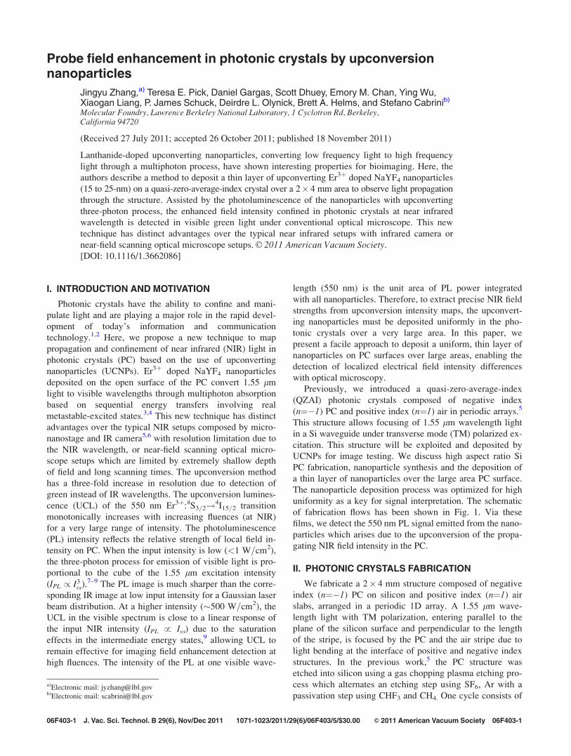
with a sidewall slope of 90�. The ICP etching results are
shown in Fig. 2. The sample is then cleaned by RCA1
(NH4OH: H2O2:H2O ¼1:1:5) and RCA3 (HCl: H2O2:
H2O¼1:1:6) at 80 �C to remove organic and metallic contami-
nants for nanoparticles deposition.
III. NANOPARTICLE SYNTHESIS
The b-NaYF4: 10% Er3þ nanoparticles were synthesized
using a modification of a recently reported procedure.15,16
Oleic acid was used as the surfactant, to control the size and
shape of the NaYF4: Er3þ nanoparticles, which showed dif-
ferent shapes when the concentration of oleic acid was
changed. Nanoparticles were drop-cast from a hexane dis-
persion and characterized by SEM, x ray diffraction (XRD)
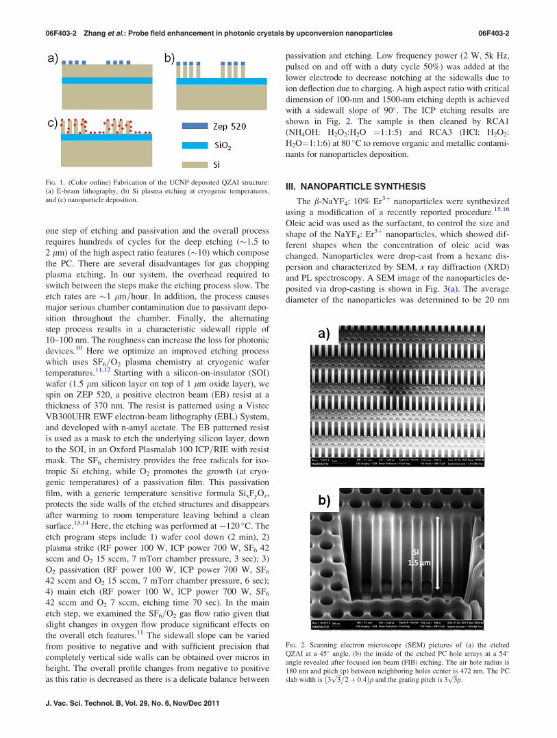
and PL spectroscopy. A SEM image of the nanoparticles de-
posited via drop-casting is shown in Fig. 3(a). The average
diameter of the nanoparticles was determined to be 20 nm
FIG. 1. (Color online) Fabrication of the UCNP deposited QZAI structure:
(a) E-beam lithography, (b) Si plasma etching at cryogenic temperatures,
and (c) nanoparticle deposition.
FIG. 2. Scanning electron microscope (SEM) pictures of (a) the etched
QZAI at a 45� angle, (b) the inside of the etched PC hole arrays at a 54�
angle revealed after focused ion beam (FIB) etching. The air hole radius is
180 nm and pitch (p) between neighboring holes center is 472 nm. The PC
slab width is 3ffiffiffi3p �
2þ 0:4� �
p and the grating pitch is 3ffiffiffi3p
p.
06F403-2 Zhang et al.: Probe field enhancement in photonic crystals by upconversion nanoparticles 06F403-2
J. Vac. Sci. Technol. B, Vol. 29, No. 6, Nov/Dec 2011
with a range of 65 nm. The nanoparticle samples were char-
acterized by XRD utilizing a Bruker D8-Discover x-ray
diffractometer. Samples were drop-cast onto thin glass cover
slips from hexanes and allowed to dry. The XRD pattern [Fig.
3(b)] shows that pure b-NaYF4 nanoparticles were obtained
and the peaks match well with the standard spectral lines of
b-NaYF4 [JCPDS #(01-077-0936)]. The PL spectrum of the
Er3þ doped nanoparticles with 1.55 lm CW diode laser
(Power density ¼ 500 W=cm2) excitation are shown in Fig.
3(c). The emission bands can be assigned to transitions within
the 4f manifolds of the Er3þ ions. The strongest two emission
bands, green emissions at 550 nm and red emission at 670 nm
is due to transitions from the 4S3=2 to 4I15=2 and 4F9=2 to 4I15=2
manifolds,17 respectively. The Er3þ doped NaYF4 nanopar-
ticles with visible emission under NIR excitation will probe
field enhancement at NIR in the QZAI photonic crystal.
IV. NANOPARTICLE DEPOSITION ON PHOTONICCRYSTAL
For deposition of the nanoparticles, the surface properties
of both the nanoparticles and that Si PC are critical. Nonpo-
lar hydrophobic molecules prefer other hydrophobic mole-
cules and nonpolar solvents whereas hydrophilic molecules
have a tendency to cling to other hydrophilic molecules.
During the synthesis process, b-NaYF4 nanoparticles are
ultimately passivated with hydrophobic oleate ligands and
dispersed in hexanes to form colloidal solutions with hydro-
phobic properties.
For surface compatibility with the oleate terminated
nanopartices, we treat the Si PC with a hydrophobic layer.
A fluoroakylsilane (FAS) in particular, 1H, 1H, 2H,
2H-perfluorodecyltri-chlorosilane (CF3(CF2)7(CH2)2SiCl3),
is applied to the Si PC to create a hydrophobic surface.18
FAS is deposited at a temperature 90 �C for 10 min – 1 h.
Contact angle measurements after 10 min give a water con-
tact angle of 110�. After FAS treatment of the PC, the nano-
particles are deposited. The PC sample is placed in a beaker
containing the particle dispersion in hexanes with silicon
substrate lean against the beaker sidewall with the PC
trenches perpendicular to the beaker bottom. We leave the
sample evaporating (2–3 h) in a ventilation hood until the so-
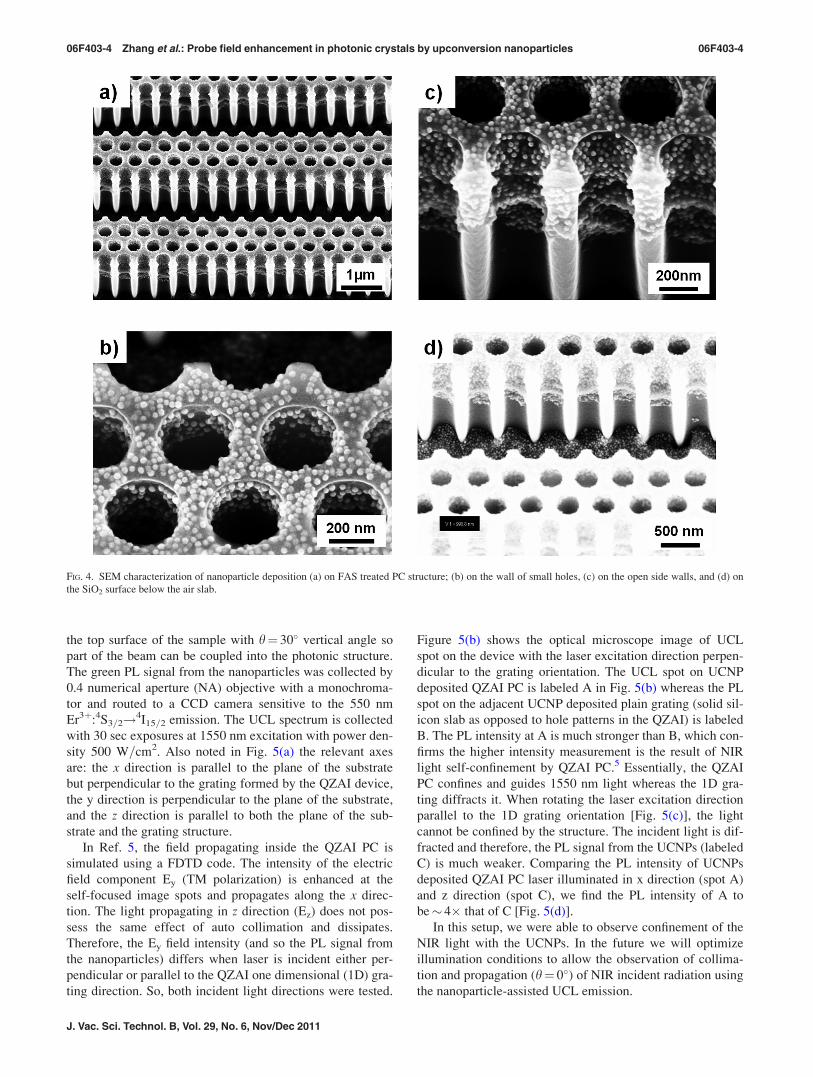
lution dries leaving the nanoparticles behind. Figure 4 shows
SEM images of nanoparticles deposited on the PC crystal.
We observe a layer of nanoparticles covering the PC struc-
ture over the entire 2-� 4-mm area. The SEM picture of
sample is shown in Fig. 4(a). The images with large magnifi-
cation are shown in Figs. 4(b), 4(c) and 4(d). Particles are
not only visible on the open side walls, but also in the inte-
rior walls of small holes and on the unpatterned SiO2 areas.
At the bottom of the vertical sections of the PC as shown in
Fig. 4(c) and 4(d), particles were not always deposited. We
attribute this to inefficient FAS coverage on the surface as
increasing the FAS deposition time to 1 h promoted the cov-
erage of particles over the entire vertical PC features.
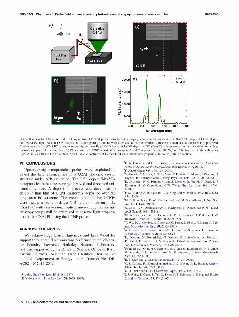
V. CHARACTERIZATION
To evaluate the functionality of the upconverting nano-
particles as probe for NIR light, we compare green light
UCL images of the QZAI device and adjacent plain silicon
grating both decorated with the nanoparticles. The experi-
mental setup is schematically illustrated in Fig. 5(a). The
QZAI device is illuminated with a continuous wave (CW)
laser at 1550 nm wavelength. The laser spot is focused on
FIG. 3. Characterization of the 10 % Er3þ doped b-NaYF4:Er nanoparticles,
(a) SEM image, (b) Powder X-ray diffraction (XRD) pattern, and c) PL
spectrum with 1550 nm CW laser excitation (Power density¼ 500 W=cm2).
The green emission at 550 nm and red emission at 670 nm indicate the Er
energy transitions from 4S 3=2 to 4I15=2 and 4F9=2 to 4I 15=2, respectively.17
06F403-3 Zhang et al.: Probe field enhancement in photonic crystals by upconversion nanoparticles 06F403-3
JVST B - Microelectronics and Nanometer Structures
the top surface of the sample with h¼ 30� vertical angle so
part of the beam can be coupled into the photonic structure.
The green PL signal from the nanoparticles was collected by
0.4 numerical aperture (NA) objective with a monochroma-
tor and routed to a CCD camera sensitive to the 550 nm
Er3þ:4S3=2!4I15=2 emission. The UCL spectrum is collected
with 30 sec exposures at 1550 nm excitation with power den-
sity 500 W=cm2. Also noted in Fig. 5(a) the relevant axes
are: the x direction is parallel to the plane of the substrate
but perpendicular to the grating formed by the QZAI device,
the y direction is perpendicular to the plane of the substrate,
and the z direction is parallel to both the plane of the sub-
strate and the grating structure.
In Ref. 5, the field propagating inside the QZAI PC is
simulated using a FDTD code. The intensity of the electric
field component Ey (TM polarization) is enhanced at the
self-focused image spots and propagates along the x direc-
tion. The light propagating in z direction (Ez) does not pos-
sess the same effect of auto collimation and dissipates.
Therefore, the Ey field intensity (and so the PL signal from
the nanoparticles) differs when laser is incident either per-
pendicular or parallel to the QZAI one dimensional (1D) gra-
ting direction. So, both incident light directions were tested.
Figure 5(b) shows the optical microscope image of UCL
spot on the device with the laser excitation direction perpen-
dicular to the grating orientation. The UCL spot on UCNP
deposited QZAI PC is labeled A in Fig. 5(b) whereas the PL
spot on the adjacent UCNP deposited plain grating (solid sil-
icon slab as opposed to hole patterns in the QZAI) is labeled
B. The PL intensity at A is much stronger than B, which con-
firms the higher intensity measurement is the result of NIR
light self-confinement by QZAI PC.5 Essentially, the QZAI
PC confines and guides 1550 nm light whereas the 1D gra-
ting diffracts it. When rotating the laser excitation direction
parallel to the 1D grating orientation [Fig. 5(c)], the light
cannot be confined by the structure. The incident light is dif-
fracted and therefore, the PL signal from the UCNPs (labeled
C) is much weaker. Comparing the PL intensity of UCNPs
deposited QZAI PC laser illuminated in x direction (spot A)
and z direction (spot C), we find the PL intensity of A to
be� 4� that of C [Fig. 5(d)].
In this setup, we were able to observe confinement of the
NIR light with the UCNPs. In the future we will optimize
illumination conditions to allow the observation of collima-
tion and propagation (h¼ 0�) of NIR incident radiation using
the nanoparticle-assisted UCL emission.
FIG. 4. SEM characterization of nanoparticle deposition (a) on FAS treated PC structure; (b) on the wall of small holes, (c) on the open side walls, and (d) on
the SiO2 surface below the air slab.
06F403-4 Zhang et al.: Probe field enhancement in photonic crystals by upconversion nanoparticles 06F403-4
J. Vac. Sci. Technol. B, Vol. 29, No. 6, Nov/Dec 2011
VI. CONCLUSIONS
Upconverting nanoparticles probes were exploited to
detect the field enhancement in a QZAI photonic crystal
structure under NIR excitation. The Er3þ doped b-NaYF4
nanoparticles in hexane were synthesized and dispersed uni-
formly by size. A deposition process was developed to
ensure a thin film of UCNP uniformly deposited over the
large area PC structure. The green light emitting UCNPs
were used as a probe to detect NIR field confinement in the
QZAI PC with conventional optical microscopy. Future mi-
croscopy setups will be optimized to observe light propaga-
tion in the QZAI PC using the UCNP probes.
ACKNOWLEDGMENTS
We acknowledge Bruce Harteneck and Erin Wood for
support throughout. This work was performed at the Molecu-
lar Foundry Lawrence Berkeley National Laboratory,
and was supported by the Office of Science, Office of Basic
Energy Sciences, Scientific User Facilities Division, of
the U.S. Department of Energy under Contract No. DE-
AC02—05CH11231.
1S. John, Phys Rev. Lett. 58, 2486 (1987).2E. Yablonovitch, Phys Rev. Lett. 58, 2059 (1987).
3D. R. Gamelin and H. U. Gudel, Upconversion Processes in TransitionMetal and Rare Earth Metal Systems (Springer, Berlin, 2001).
4F. Auzel, Chem Rev. 104, 139 (2004).5V. Mocella, S. Cabrini, A. S. P. Chang, P. Dardano, L. Moretti, I. Rendina, D.
Olynick, B. Harteneck, and S. Dhuey, Phys Rev. Lett. 102, 133902 (2009).6R. Chatterjee, N. C. Panoiu, K. Liu, Z. Dios, M. B. Yu, M. T. Doan, L. J.
Kaufman, R. M. Osgood, and C.W. Wong, Phys Rev. Lett. 100, 187401
(2008).7P. S. Golding, S. D. Jackson, T. A. King, and M. Pollnau, Phys Rev. B 62,
856 (2000).8M. P. Hasselbeck, E. W. Van Stryland, and M. Sheik-Bahae, J. Opt. Soc.
Am. B 14, 1616 (1997).9G. Chen, T. Y. Ohulchanskyy, A. Kachynski, H. Agren, and P. N. Prasad,
ACS Nano 5, 4981 (2011).10M. W. Pruessner, W. S. Rabinovich, T. H. Stievater, D. Park and J. W.
Baldwin, J. Vac. Sci. Technol. B 25, 21 (2007).11Y. Wu, D. L. Olynick, A. Goodyear, C. Peroz, S. Dhuey, X. Liang, S. Cab-
rini, Microelectron. Eng. 88, 2785 (2011).12A. F. Isakovic, K. Evans-Lutterodt, D. Elliott, A. Stein, and J. B. Warren,
J. Vac. Sci. Technol. A 26, 1182 (2008).13R. Dussart, M. Boufnichel, G. Marcos, P. Lefaucheux, A. Basillais,
R. Benoit, T. Tillocher, X. Mellhaoui, H. Estrade-Szwarckopf, and P. Ran-
son, J. Micromech. Microeng. 14, 190 (2004).14M. de Boer, J. G. E. H. Gardeniers, H. V. Jansen, E. Smulders, M. J. Gilde,
G. Roelofs, J. N. Sasserath and M. Elwenspoek, J. Microelectromech.
Syst. 11, 385 (2002).15H. S. Qian and Y. Zhang, Langmuir, 24, 12123 (2008).16C.-J. Carling, F. Nourmohammadian, J.-C. Boyer, N. R. Branda, Angew.
Chem. Int. Ed. 49, 3782 (2010).17G. H. Dieke and H. M. Crosswhite, Appl. Opt. 2, 675 (1963).18J. J. Wang, L. Chen, S. Tai, X. Deng, P. F. Sciortino, J. Deng, and F. Liu,
J. Lightw. Technol., 23, 474 (2005).
FIG. 5. (Color online) Measurement of PL signal from UCNP deposited structures (a) imaging setup and illumination axes; (b) CCD images of UCNP depos-
ited QZAI PC (spot A) and UCNP deposited silicon grating (spot B) with laser excitation predominantly in the x direction and the laser is p-polarized.
Confinement by the QZAI PC causes A to be brighter than B; (c) CCD image of UCNP deposited PC (Spot C) at laser excitation in the z direction with p-
polarization; parallel to the surface; (d) PL spectrum of UCNP deposited PC for spots A and C at power density 500 W=cm2. The intensity in the x direction
(Spot A) is� 4 x that in the z direction (Spot C) due to confinement by the QZAI when illuminated perpendicular to the grating direction.
06F403-5 Zhang et al.: Probe field enhancement in photonic crystals by upconversion nanoparticles 06F403-5
JVST B - Microelectronics and Nanometer Structures