Embed Size (px)
Citation preview

PRGA: An Open-Source FPGA Research andPrototyping Framework
Ang Liangl(at)princeton(dot)edu
Princeton UniversityPrinceton, New Jersey
David Wentzlaffwentzlaf(at)princeton(dot)edu
Princeton UniversityPrinceton, New Jersey
ABSTRACTField Programmable Gate Arrays (FPGA) are being used in a fast-growing range of scenarios, and heterogeneous CPU-FPGA systemsare being tapped as a possible way to mitigate the challenges posedby the end of Moore’s Law. This growth in diverse use cases hasfueled the need to customize FPGA architectures for particularapplications or application domains. While high-level FPGAmodelscan help explore the FPGA architecture space, as FPGAs move tomore advanced design nodes, there is an increased need for low-level FPGA research and prototyping platforms that can be broughtall the way to fabrication.
This paper presents Princeton Reconfigurable Gate Array(PRGA), a highly customizable, scalable, and complete open-sourceframework for building custom FPGAs. The framework’s core func-tions include generating synthesizable Verilog from user-specifiedFPGA architectures, and providing a complete, auto-generated,open-source CAD toolchain for the custom FPGAs. Developed inPython, PRGA provides a user-friendly API and supports use bothas a standalone FPGA as well as an embedded FPGA. PRGA is agreat platform for FPGA architecture research, FPGA configurationmemory research, FPGA CAD tool research, and heterogeneoussystems research. It is also a completely open-source frameworkfor designers who need a free and customizable FPGA IP core. AnFPGA designed with PRGA is placed and routed using standardcell libraries. The design is evaluated and compared to prior works,providing comparable performance and increased configurability.
CCS CONCEPTS• Hardware→ Reconfigurable logic and FPGAs.
KEYWORDSFPGA; FPGA architecture; open-source hardwareACM Reference Format:Ang Li and David Wentzlaff. 2021. PRGA: An Open-Source FPGA Researchand Prototyping Framework. In Proceedings of the 2021 ACM/SIGDA Interna-tional Symposium on Field Programmable Gate Arrays (FPGA ’21), February28-March 2, 2021, Virtual Event, USA. ACM, New York, NY, USA, 11 pages.https://doi.org/10.1145/3431920.3439294
Permission to make digital or hard copies of all or part of this work for personal orclassroom use is granted without fee provided that copies are not made or distributedfor profit or commercial advantage and that copies bear this notice and the full citationon the first page. Copyrights for components of this work owned by others than theauthor(s) must be honored. Abstracting with credit is permitted. To copy otherwise, orrepublish, to post on servers or to redistribute to lists, requires prior specific permissionand/or a fee. Request permissions from [email protected] ’21, February 28-March 2, 2021, Virtual Event, USA© 2021 Copyright held by the owner/author(s). Publication rights licensed to ACM.ACM ISBN 978-1-4503-8218-2/21/02. . . $15.00https://doi.org/10.1145/3431920.3439294
1 INTRODUCTIONField Programmable Gate Arrays (FPGAs) have become an in-creasingly important tool to enable application performance ina post Moore’s Law [19] world. Whether they are being used asa standalone compute fabric or a supplement to processors at thechip-level [8, 10, 29], board-level [20], system-level, or datacenter-level [1, 5], the diversity of use cases and importance of FPGAshave been increasing. Ideally, an FPGA architecture should be op-timized for each unique use case. In practice, though, it is verychallenging to evaluate different FPGA designs in detail and evenmore challenging and time-consuming to prototype and bring thoseFPGAs to fabrication. This is because FPGA chip design flow hasdiverged from the design flows of other digital ASICs like pro-cessors. Commercial FPGAs are often designed with custom cellsand specialized EDA tools that are publicly unavailable. Likewise,each unique FPGA requires the creation of customized CAD tools.Due to this high design cost, commercial FPGA vendors typicallyoffer a limited set of designs optimized across common, but poten-tially non-characteristic, use cases. Due to similar reasons, FPGAarchitecture studies often use and stop at high-level models [4, 21].
To facilitate FPGA architecture research and enable designs op-timized for custom applications, tools are needed to evaluate, opti-mize, and prototype FPGA architectures all the way down to thefabrication level. An ideal framework would be easy-to-use, exten-sible, scalable, and open-source. A framework that provides synthe-sizable RTL enables gate-level or transistor-level implementationusing commercial ASIC design flows and standard cell libraries. Byenabling such physical prototyping, a framework can be used toevaluate timing, power, and area with the utmost fidelity. Likewise,RTL-level prototyping incorporates the details of the configurationmemory, enabling research on bitstream format and partial or dy-namic reconfiguration. High-level modeling tools are an importantfirst step, but there exists a need for low-level (RTL and below)frameworks that can be used to study low-level issues such asfloorplanning, design regularity, signal integrity, and other physicaldesign issues all while providing the path to then take the optimizeddesign through prototyping and fabrication.
In this paper, we present Princeton Reconfigurable GateArray (PRGA), a highly customizable, scalable, and completeopen-source framework for building custom FPGAs. PRGA isavailable at https://parallel.princeton.edu/prga. Fig. 1 showsthe workflow used to design a custom FPGA and then develop anapplication that uses it. The PRGA FPGA architecture is highlycustomizable, and it supports user-provided modules such as SRAMmacros, hard arithmetic units, and routing switches, all of whichcan be easily added into the flow. PRGA is developed in Python andprovides a well-defined Python API. Extensions are encouraged and

Figure 1: Overview of a typical PRGA workflow
supported through modularization and low-level APIs. To furtherlower the barrier of extending the framework, most output filesare generated from human-readable Jinja [25] templates that arecustomizable without changing the Python codebase. At the end ofthe FPGA design flow, PRGA produces human-readable, industry-standard, Verilog files that are synthesizable and physically imple-mentable using commercial EDA Tools. PRGA is ASIC-friendly andcan be used to generate standalone FPGAs as well as embeddedFPGAs, where the customization that PRGA provides is critical.
PRGA is not derived from prior FPGA modeling/explorationtools. Therefore, it is not restricted by the internal representationsof legacy tools. This enables PRGA to support flexible hierarchiesthat match physical implementation needs. Likewise, the generatedconfiguration circuitry is highly flexible and is decoupled from thedesign hierarchy, opening up the ability for researchers to explorenovel configuration strategies (order, storage, and topology) whichis a key component to building efficient FPGAs. Such physical-aware customizability is critical to the design of large-scale, high-performance, fabrication-ready FPGAs.
In addition to designing the FPGA itself, PRGA offers a completeHDL-to-bitstream solution using open-source CAD tools, config-uring and parameterizing those FPGA implementation CAD toolsfor the created custom FPGA. Specifically, this flow uses Yosys [28]for technology mapping and synthesis, VPR [21] for place & route,FASM [23] for raw bitstream generation, and a custom bitstreamgenerator to convert the raw bitstream into binary format. Thetarget application can be verified by simulation with various levelsof abstraction throughout the flow, making it easy to debug boththe FPGA itself and the application. Scripts and data files for thesame FPGA are reusable across application development runs.
In summary, the key features of PRGA include:• Architecture Customizability(1) Fully-customizable, heterogeneous logic blocks: LUT count,
LUT size, local interconnect, hard adder chains, multi-modalprimitives, logic elements, and more.
(2) Bring-Your-Own-IP: block RAM, hardened multiplier/accu-mulator, and even big IP cores like CPUs, memory/networkcontrollers, etc.
(3) Fully-customizable routing structure: switch box pattern,connection box pattern, non-uniform channel, long wires,and global wires.
(4) Extensible configuration circuitry: simple scanchain-basedconfiguration or complex, NoC-based, packetized bitstreams
with support for partial reconfiguration. Custom configura-tion circuitry can also be designed using low-level API.
• CAD Support(1) Auto-generated Yosys script for synthesis: BRAM inference,
hard logic techmap, and post-synthesis simulation.(2) Auto-generated, FASM-annotated VPR inputs for place-
ment, routing and raw bitstream generation.• ASIC Compatibility(1) Bring-Your-Own-Circuits: replace generated modules with
custom Verilog modules or hard macros.(2) ASIC-friendly module hierarchy: fracturable switch box
to maximize regularity; arbitrary levels of sub-arrays tobalance ASIC QoR and ease-of-backend.
• Framework Extensibility(1) Modularized, pass-based workflow. Passes may be added
or modified without affecting the rest of the flow.(2) Core data structure can be serialized to disk. Tools don’t
need to rerun the entire building process every time.In this paper, we evaluate PRGA by characterizing its scalability
in terms of memory usage and runtime and find that it enablesthe creation of very large designs with reasonable computationalresources. In addition, we take a design through place and route totape-in quality to show that PRGA is production-ready. Finally, wecompare designs created with PRGA with prior and commercialdesigns in terms of area and delay, and show that we are competitivewith other standard-cell-based FPGA generators.
PRGA enables many exciting applications. It is a great platformfor FPGA architecture research, in particular bridging the gap fromhigh-level FPGA architecture exploration tools down to low-levelimplementation details, as well as enabling RTL-in-the-loop FPGAarchitecture optimization studies. It can also be used to build targetsfor FPGA CAD tool research, for example, security-aware place-and-route tools. PRGA is a framework that allows the creation andexploration of many different FPGA designs, which makes it morethan an FPGA generator that can only generate a certain type ofFPGA. The FPGAs built with PRGA can be used either as standaloneFPGAs or integrated into SoCs. It can even be an excellent platformfor CPU-FPGA heterogeneous system research.
2 PRGAWORKFLOWFig. 1 shows an overview of a typical PRGA workflow. The FPGAdesign flow is driven by a user-written Python script, while theHDL-to-bitstream flow integrates open-source CAD tools to generatevalid bitstreams for the created custom FPGA.

Figure 2: FPGA architecture modeled by PRGA. The position, shape and size of the modules do not reflect the physical prop-erties in an ASIC implementation. Programmable connections are shown as many-to-one connections in routing boxes andblocks. 1○ are bridging nets discussed in Sec. 3.3.3; 2○ is an unroutable clock pin directly connected to the global clock tree.
2.1 Database PreparationPRGA offers various basic components for building an FPGA, includ-ing look-up tables (LUT) and registers. However, it is common thatFPGA designers want to add custom components into the design,for example, SRAM macros, hard arithmetic units, or even complexIP cores such as memory controllers. These components are clas-sified as Logic Primitives in PRGA and elaborated in Sec. 3.3.1.During the database preparation step, users can add custom LogicPrimitives by creating proper models for them, whether they arehard macros or synthesizable HDL designs.
2.2 Architecture CustomizationAfter database preparation, the users can build the desired customFPGA architecture by creating programmable blocks and assem-bling them in a hierarchical manner, as shown in Fig. 2. In summary,the top level of the hierarchy is a 2-dimensional Array composed ofTiles, Switch Boxes, and nested Arrays. Each Tile contains oneLogic Block or multiple IO Blocks, in addition to various num-bers of Connection Boxes. Logic Blocks and IO Blocks consistof zero to many Slices and Logic Primitives. Last but not least,Slices are composed of nested Slices and Logic Primitives.Each of these modules will be discussed in detail in Sec. 3.
One key feature of PRGA is the decoupling of the functionalabstraction of the FPGA, the underlying configuration circuitry,and the physical implementation of the circuits. During architecturecustomization, FPGA designers can focus on describing the logicalfunction and connectivity, and leave the implementation details tolater steps that are independently customizable. For example, tocreate a configurable connection in a Logic Block, users do notneed to explicitly specify how the MUX tree should be constructed,or the order of the configuration bits for the MUXes.
The high customizability of PRGA opens up a huge design spacefor exploration, which is critical to architecture researchers andexperienced FPGA designers with specific needs. On the other hand,to make this highly flexible framework easy to use for new users,PRGA provides abundant built-in algorithms to ease the generationof decent FPGAs from meta parameters. For example, while routingboxes are customizable on a per-wire, per-connection basis, variousdefault algorithms are provided for populating them, includingFc-based Connection Box patterns [4], Universal [6], Wilton [27],and Cycle-Free [15] Switch Box patterns, etc.
2.3 Transformation and Generation PassesPRGA does all the heavy-lifting work through transformation andgeneration passes. The passes shown in Fig. 1 are the most com-monly used ones:
Configuration Circuitry Insertion expands the functional, abstractdescription of the FPGA by elaborating the configuration circuitryand implementing the configurable connectionswith programmableswitches. The configuration circuitry does not need to match thelogical design hierarchy. Typically, each type of configuration cir-cuitry has its own implementation of this pass.
Synthesis Script Generation discovers all the logical resourcesavailable in the FPGA, then generates technology mapping andsynthesis scripts for mapping applications onto the custom FPGA.
Place and Route Script Generation generates the XML files neededby VPR [21] to place and route for the FPGA. To accurately modelthe highly customizable routing resources, PRGA generates theRouting Resource Graph XML in addition to the Architecture Descrip-tion XML. PRGA uses FASM [23] for raw bitstream generation, soadditional annotations are added to the XML files accordingly.
RTL Generation generates industry-standard, human-readable,synthesizable Verilog files for the FPGA. As mentioned in Sec. 1,PRGA uses Jinja [25] for text file generation, and the templates canbe changed without affecting the rest of PRGA.
Passes may be bound to specific execution order constraints,depend on other passes, or conflict with each other. For example,RTL Generation depends on Configuration Circuitry Insertion tofill in the physical implementations of the abstract architecturespecifications, while Configuration Circuitry Insertion passes fordifferent types of configuration circuitry conflict with each other.Graph analysis algorithms are applied to determine the correctexecution order of passes, making it easier to add or modify passes.In addition to these built-in passes, users are encouraged and well-supported to add their own passes to optimize, analyze and createcustom reports for their custom FPGAs.
2.4 ASIC ImplementationPRGA is designed and optimized with a strong emphasis on en-abling gate-/transistor-level prototyping or even fabrication, espe-cially as a target of modern ASIC design flow using commercialEDA tools and standard cell libraries. Common ASIC implementa-tion techniques are taken into consideration during RTL generation.

For example, the configuration enable signal is registered at dif-ferent levels across the hierarchy to reduce potential skew of thishigh-fanout net. In addition, the flexible hierarchy and customizableRTL generation grant FPGA designers the freedom to explore andoptimize the layout strategy specific to their process and design.
2.5 Application Development and VerificationAll the files required by the open-sourceHDL-to-bitstream toolchainare generated by the generation passes in the FPGA design flow,and they can be reused across different runs of the application de-velopment and verification flow. Furthermore, PRGA offers variousexecutable Python scripts for generating the Verilog testbenches,constraints, and Makefiles to automate the flow. A valid and verifiedbitstream is thus only a few commands away from the HDL inputs.
With the RTL-level model of the FPGA, we can simulate theFPGA from power-on reset, bitstream loading, all the way to appli-cation emulation. This Emulation-over-Simulation approach offersgreat fidelity of the architecture, and simplifies debugging both theFPGA and the application. Moreover, after pushing the RTL throughan ASIC implementation flow, we can run gate-/transistor-levelsimulation with more accurate timing and power characteristics.
3 ARCHITECTUREIn this section, we describe PRGA’s highly flexible and customizablearchitecture.
3.1 Routing ResourcesPRGA currently supports straight, uni-directional routing tracks,global nets, and direct inter-block wires. Routing tracks, also calledwire segments, are grouped by length in the unit of logical tiles. Bydefault, PRGA fills every routing channel in the custom FPGA withall groups of tracks. However, if certain tracks are not driven by anySwitch Box or Connection Box, they are depopulated from the spe-cific routing channel, enabling per-wire, per-channel customization.We intentionally dropped support for bi-directional routing tracksbecause they are not compatible with common ASIC implementa-tion flows, and they are no longer used in newer generations ofcommercial FPGAs either. Global nets and direct inter-block wires(Tunnels in PRGA’s terminology) are non-programmable routingresources. Global nets are typically used for clock or reset trees,while Tunnels are usually used to implement fast carry-chains.
3.2 ViewsAs outlined in Sec. 2.2, PRGA decouples the logical abstraction,configuration circuitry, and physical implementation of the FPGAto maximize modularization. This is achieved by using differentViews, a concept borrowed from the EDA world, at different stepsthroughout the FPGA design flow:
The Abstract View offers a high-level abstraction of the archi-tecture. It is primarily used during the architecture customizationand CAD script generation steps.
The Design View is usually the output of the ConfigurationCircuitry Insertion pass, implementing the Abstract View specifiedby users. Synthesizable Verilog can be generated from this view.
The Physical View offers more flexibility over the Design Viewand is primarily reserved for extensions. One typical use of this
(a) Two modes in Abstract View
(b) Design View implemented with the Scanchainconfiguration circuitry. Mode selection bit high-lighted with red box and arrow.
Figure 3: Different views of a fracturable LUT3 which can beused as one single LUT3, or two LUT2s with shared inputs.
view is to generate RTL files for ASIC implementation, which aredifferent from those used in simulation.
3.3 Hierarchy and CustomizabilityIn this section, we dive into how PRGA organizes the hierarchy ofthe FPGA architectures and show the customizability of each levelin the hierarchy.
3.3.1 Logic Primitive. Also known as logic elements or logic re-sources, Logic Primitives are the building blocks of FPGAs. InPRGA, all hard logic that is targeted by technology mapping andsynthesis are categorized as Logic Primitives, including but notlimited to LUTs, flip-flops, hard arithmetic units, SRAM macros, oreven complex IP cores like memory controllers.
Logic Primitives are further classified into three types:
• Non-Programmable primitives, e.g., simple flip-flops.• Programmable primitives, e.g., LUTs. The functions providedby these primitives are altered by configuration.
• Multi-Modal primitives, e.g., fracturable LUTs. These prim-itives can be configured to one of its many modes, eachoffering a unique function. Multi-modal primitives are notdirectly targeted by synthesis. Instead, logical primitives em-ulated by its various modes are targeted by synthesis, thenmatched with the corresponding mode during packing.
Ideally, we would like to design primitives in a configuration-agnostic manner to maximize reusability and extensibility. Unfortu-nately, this is not always feasible. For example, LUTRAM, one modeof a LUT which can be used as a RAM, requires the capability ofwriting to the underlying configuration memory. Addressing thisissue, PRGA exploits the views as discussed in Sec. 3.2. PRGA usesthe Abstract View to specify the logical function of a primitive,and uses the Design View for the actual implementation. Fig. 3shows the two Abstract Views and one Design View of a "fracr-turable" LUT3, which can be used as one single LUT3, or two LUT2swith shared inputs.

All three types of primitives are customizable in PRGA. Non-programmable primitives can be easily added by creating newLogic Primitive objects with their interfaces and Verilog sourcefiles. Programmable primitives can be added in a similar way, onlythat an additional Design View matching the selected configu-ration circuitry is required. Multi-modal primitives require morehands-on development: Each mode of a multi-modal primitive issimilar to a Slice in the Abstract View. A Design View imple-menting all the different modes and the mode-selection mechanismspecific to the selected configuration circuitry is also required.
3.3.2 Slice, Logic Block, and IO Block. Slices (also called ALMsor clusters), Logic Blocks, and IO Blocks are modules built uponLogic Primitives, as shown in Fig. 2 (c). The purpose of thesemodules are three-fold: For the FPGA CAD tools, they serve as thetargets for packing aswell as routing terminals for place & route; ForRTL-level simulation, they serve as hierarchical wrappers aroundLogic Primitives, making the latter easier to monitor and debug;For ASIC implementation, they can be designed as the lowest-levelphysical block and reused across the chip, minimizing performancevariation across block instances.
Logic Blocks may be logically wide, tall, or both, spanningacross multiple tiles. It is also configurable if routing tracks areallowed to run through or over these large blocks. This logical sizeonly affects the topology of the routing resources around it, andmaymismatch the physical size or shape in the ASIC implementation.
3.3.3 Connection Box and Switch Box. Routing boxes are catego-rized into two classes in PRGA: Connection Boxes that connectrouting tracks to the pins of Logic Blocks and IO Blocks; andSwitch Boxes that connect routing tracks to other routing tracks.
By default, each side (north, east, south, and west) of a blockneeds a Connection Box, although it is very common to omit someConnection Boxes when there are no routable pins on certainsides of a block. Fig. 2 (c) shows an example where ConnectionBoxes are only needed on the east and west side of the Logic Block.Creatingmore Connection Boxes for the same side of a block is alsosupported, enabling fine-grained customization around differentinstances of the same block. For tall and wide blocks, the numberof Connection Boxes needed on each side is equal to the width orheight of the block.
Switch Boxes are modeled in a highly flexible way. As shownin Fig. 2 (a) & (b), each corner (northeast, northwest, southeast,and southwest) in a tile fits one Switch Box, allowing up to 4Switch Boxes wherever routing channels cross, although it’s notnecessary to fill all corners. No limit is set on the number of distinctSwitch Boxes used across the FPGA, though in practice, a smallset of Switch Boxes are often reused to reduce design complexity.
Since uni-directional routing tracks cannot have more than onedriver, a Connection Box may conflict with a Switch Box whenthey drive the same routing track. To solve this conflict, PRGA addsbridging nets to connect Connection Box outputs into SwitchBoxes and merges them to the switches inside Switch Boxes, ashighlighted in Fig. 2 (b).
3.3.4 Tile. A Tile wraps one Logic Block instance or multipleinstances of an IO Block, together with the Connection Boxesaround them. Fig. 2 (c) shows a tile wrapping one Logic Block
and two Connection Boxes. Multiple Tiles can be created for thesame block, enabling the usage of different Connection Boxes asmentioned in Sec. 3.3.3. Helper functions are provided for automat-ically generating Tiles for each block, as well as properly creating,populating, and instantiating Connection Boxes.
This extra level of hierarchy is primarily aimed to improve ASICimplementation, and may be useful for certain configuration pro-tocols. When used as the lowest-level physical block other thanthe Logic Block wrapped in it, it allows the EDA tools to workon a larger design and exploit more optimization opportunities,while guaranteeing that each Logic Block has only one physicalimplementation.
3.3.5 Array. The top level in the FPGA architecture hierarchy isan Array composed of Tiles, Switch Boxes, and nested Arrays.Fig. 2 (a) & (b) shows the nesting and internals of Arrays. EachArray is a 2-dimensional mesh. Each tile in the mesh can accom-modate up to four Switch Boxes (one on each corner) plus oneTile or Array. Large Tiles or Arrays may occupy more than onetile. Switch Boxes are not allowed at any routing channel cross-points that are covered by these large Tiles or Arrays, and routingtracks around them are truncated if not allowed to run throughor over them. PRGA offers helper functions for automatically, cor-rectly connecting the wires in an Array. If any built-in routing boxpopulation algorithm is used, PRGA can also automatically create,populate and instantiate proper Switch Boxes.
PRGA offers great regularity and scalability through the useof nested Arrays. Special configuration circuitry features such aspartial or dynamic reconfiguration can also take advantage of thisflexible hierarchy. For example, to implement partial dynamic recon-figuration, we can divide the FPGA into dynamically reconfigurableregions, each region being an Array. We can add one configurationcontroller per region and expose a well-defined interface of thecontroller into adjacent regions, enabling dynamic reconfigurationfrom adjacent regions.
3.4 Configuration CircuitryConfiguration circuitry, including memory cells and peripheral cir-cuits, is one of the biggest commercial secrets in the FPGA industryyet is often neglected in FPGA architecture research, despite it mak-ing up a large proportion of on-chip area (20%-40% reported [12, 14])and static energy consumption. Studying and modeling configura-tion circuitry is necessary to fully understand FPGA architectureimplications. In addition, optimization of configuration circuitryenables novel architectures [7, 9, 11, 16].
Two types of configuration circuitry and comprehensive sup-ports for them are included in PRGA at the time of this paper:Scanchain and Pktchain, respectively.
3.4.1 Scanchain. As its name suggests, Scanchain employs a shiftregister chain across the entire FPGA. The bitstream format isalso straightforwardly a literal stream of bits. The chain may besingle-bit wide or multi-bit wide, offering a trade-off between fasterconfiguration and higher metal usage. Fig. 3b shows the single-bitconfiguration chain segment inside a fracturable LUT3.
Though it seems naïve, careful design is still required to avoidpotential hazards:

• Configuration reset and enable. Even a small FPGA maycontain thousands of configuration bits, and this numbergrows quickly into millions as the size of the FPGA increases.To synchronize the reset and enable signals for this hugenumber of registers, PRGA automatically registers the resetand enable signals along the hierarchy.
• Chain orderingwith physical considerations. Logically,the registers on the chain can be ordered arbitrarily. Physi-cally, however, it is better to put the configuration bits closeto the modules they control, and order the chain so that reg-isters are connected only to adjacent registers. PRGA makesgood guesses by default, but user-provided hints are alsoaccepted.
3.4.2 Pktchain. For large FPGAs, Scanchain is not only slow butalso energy-hungry, because all the registers on the scan chainmust be enabled during programming. Pktchain addresses thisissue by dividing the single Scanchain into segments and addinghigh-bandwidth NoC routers between them. This design only addsa small amount of extra wires, minimizing the impact on metalresources that are precious for the logical routing resources. Thehigh bandwidth of the NoC allows fast delivery of the bitstreamsegments. Once delivered, each bitstream segment is independentlyshifted in the corresponding chain segment. Multiple chain seg-ments can operate in parallel, thus increasing the programmingspeed. This design also greatly reduces unnecessary switching ofthe registers, thus reducing the energy consumption.
3.4.3 Extensions. Scanchain and Pktchain are both developedupon the low-level API provided by PRGA, and they are greatproof-of-concept designs showcasing the strong extensibility of theframework. Other configuration circuitry types, for example, theindustry-standard SRAM-based design, can be added in a similarway. It is also possible to implement more complex configurationcircuitry and protocols, such as the dynamic partial reconfigurationdesign described in Sec. 3.3.5.
4 CASE STUDY: BUILDING A 14K-LUT6 FPGAIn this section, we illustrate the FPGA design flow by going throughthe process of building an example FPGA using PRGA. Fig. 4 showsthe abstract, hierarchical floorplan and the configuration circuitrysettings. Table 1 summarizes the key parameters of the FPGA. List-ing 1 shows the Python script for building this example FPGA us-ing the PRGA Python API. This FPGA provides 14240 multi-modalLUT6s, 28480 registers, 2.56Mbits memory, 1279 GPIOs, and one IOdedicated for clock.
This example design is very similar to the synthesizable FPGAspresented in prior works [12, 24]. PRGA is capable of generatingvery different architectures, and we choose the similar design sothat we can evaluate and compare our design with prior works.
4.1 Database PreparationWe choose the FLE6 multi-modal primitive used in prior works [12,24] as the basic logic element for this example FPGA. FLE6 supportstwo modes: (1) one LUT6 and an optional D-flipflop, (2) two BLEsthat are independently configurable. Each BLE also supports twomodes: (1) one LUT5 and an optional D-flipflop, (2) two LUT4s, one
(a) Floorplan of the example FPGA. Top-level Array is composedof LOGIC Arrays and IO Tiles. Each LOGIC Array consists of 89Logic Blocks (L), 5 BRAMs (M), and 1 physical-only configurationrouter (C). Each IO Tile provides 8 GPIOs. Each Logic Block con-tains 10 FLE6 (multi-modal LUT6 with hard adders and flipflops).Each BRAM provides 32Kbits memory. Routing boxes are omittedin the figure.
(b) Configuration network and chain segments
Figure 4: Floorplan and configuration circuitry of the exam-ple FPGA in Sec. 4.
hard adder, and one optional D-flipflop. The figure describing thestructure of this primitive can be found in [12].
In addition, a third-party 512 × 64𝑏 SRAM macro is added to thebuild. To give more flexibility to synthesis and packing, we can addextra muxing logic around the SRAM to support smaller word sizes,for example, 1𝐾 × 32𝑏, 2𝐾 × 16𝑏, 4𝐾 × 8𝑏, etc. This is achieved bycreating Abstract Views for each mode, writing custom Verilogfiles, and creating a Design View to link them together, as shownin line 7-40 in Listing 1 (Verilog not shown).
4.2 Architecture CustomizationAfter adding all the custom Logic Primitives, we can start cus-tomizing the FPGA architecture. First, routing tracks and global netsare added to the FPGA, as shown in line 43-46 in Listing 1. Then,we customize each Logic Block and IO Block (line 50-81). Asdiscussed in Sec. 2.2, we only need to describe the functional struc-tures of these blocks. Pack patterns (line 62) and direct inter-blockwires (line 70) are added for the carry chain. After describing theblocks, we construct Tiles (line 85-94) and Arrays (line 100-116),then adopt built-in algorithms to automatically create, populate,and instantiate routing boxes.
4.3 Transformation and Generation PassesAfter specifying the FPGA architecture, we prepare our Jinja [25]text renderer, then set up the transformation and generation passes,

Listing 1: Python script for building the example FPGA de-scribed in Sec. 4. Some API syntax is abbreviated for clarity.This script alone drives the entire FPGA design flow. It alsogenerates all the RTL as well as all the files needed by theCAD tools.
1 from prga import *
# == database preparation ==# ctx is an Context object for our workspacectx = Pktchain.new_context(noc_width=8, chain_width=1)
6# == design and add multi-modal primitive for block RAM ==# bdr is a Builder objectbdr = ctx.build_multimode(name="memory")bdr.create_clock (name="clk")
11 bdr.create_input (name="D", width=64)bdr.create_output(name="Q", width=64)# ... and more ports
# -- create abstract views for the modes --16 for name, AW, DW in [
["512x64b", 9, 64],["1K32b", 10, 32],# ... and more modes
]:21 mb = bdr.build_mode(name="mode_"+name)
# abstract view of non-programmable memory modulesdpram = ctx.build_memory(name="dpram_"+name,
addr_width=AW, data_width=DW, vpr_model="dpram",).commit()
26 inst = mb.instantiate(model=dpram, name="i_ram_core")mb.connect(mb.ports["clk"], inst.pins["clk"])mb.connect(mb.ports["D"][0:DW], inst.pins["data1"])mb.connect(inst.pins["out2"], mb.ports["Q"][0:DW])# ... and more connections
31 mb.commit()
# -- link design view --# user Verilog implementation provided by userbdr = bdr.build_logical_counterpart(
36 verilog_template="memory.v")# ... design-specific settings
# -- commit the design --memory = bdr.commit()
41# == add routing resources ==glb_clk = ctx.create_global(name="clk", is_clock=True)glb_clk.bind(position=(0, 21), subtile=0) # bind to an IOl4 = ctx.create_segment(name='L4', width=32, length=4)
46 l16 = ctx.create_segment(name='L16', width=1, length=16)
# == customize blocks ==# -- logic block --bdr = ctx.build_logic_block(name="clb")
51 clk = bdr.create_global(global_=glb_clk, side="south")in_ = bdr.create_input (name="in", width=30, side="east")ci = bdr.create_input (name="ci", width=1, side="south")out = bdr.create_output(name="out", width=20, side="east")co = bdr.create_output(name="co", width=1, side="north")
56 xbar_i, xbar_o = [], []xbar_i.extend(in_)for idx, inst in enumerate(bdr.instantiate(
model=ctx.primitives["fle6"], name="i_fle", reps=10):bdr.connect(clk, inst.pins["clk"])
61 bdr.connect(inst.pins["out"], out[idx*2:(idx+1)*2])bdr.connect(ci, inst.pins["cin"],
vpr_pack_patterns=["carrychain"])ci = inst.pins["cout"]xbar_i.extend(inst.pins["out"])
66 xbar_o.extend(inst.pins["in"])bdr.connect(ci, co)# ... connect each "xbar_o" to 50% "xbar_i"sclb = bdr.commit()
Listing 2: (Continued)70 # -- create direct inter-block wires --
ctx.create_tunnel(name="carrychain", offset=(0, -1),source=clb.ports["cout"], sink=clb.ports["cin"])
# -- IO block --75 bdr = ctx.build_io_block(name="iob")
# ... ports, instances and connectionsiob = bdr.commit()
# -- BRAM block (tall block) --80 bdr = ctx.build_logic_block(name="bram", width=1, height=2)
bdr.instantiate(model=memory, name="i_ram")# ... ports, instances and connectionsbram = bdr.commit()
85 # == automatically create and populate tiles ==# -- IO tiles --iotiles = {}for edge in ["west", "north", "east", "south"]:
bdr = ctx.build_tile(block=iob, capacity=8, edge=edge)90 bdr.fill(fc=(0.15, 0.15)).auto_connect()
iotiles[edge] = bdr.commit()
# -- CLB tile --bdr = ctx.build_tile(block=clb)
95 clbtile = bdr.fill(fc=(0.055, 0.1)).auto_connect().commit()
# -- BRAM tile --bdr = ctx.build_tile(block=bram)bramtile = bdr.fill(fc=(0.055, 0.1)).auto_connect().commit()
100# == arrays ==sb_pat = SwitchBoxPattern.cycle_free
# -- LOGIC array --105 bdr = ctx.build_array(name="logic", width=10, height=10)
for x, y in product(range(bdr.width), range(bdr.height)):if x == 5:
if y % 2 == 0:bdr.instantiate(model=bramtile, position=(x, y))
110 elif not (x == 0 and y == 0): # reserved for routerbdr.instantiate(model=clbtile, position=(x, y))
logic = bdr.fill(sbox_pattern=sb_pat).auto_connect().commit()
# -- top-level array --115 bdr = ctx.build_array(name="top", width=42, height=42,
is_top=True)# ... instantiate LOGIC arrays and IO tilestop = bdr.fill(sbox_pattern=sb_pat).auto_connect().commit()
120 # == customize configuration circuitry insertion ==# callback function for customize router & chain orderingdef order_submodules(module):
# ...
125 # == apply transformation and generation passes ==# -- Jinja2 template renderer --renderer = Pktchain.new_renderer()
# -- transformation and generation flow --130 flow = Flow(
TranslationPass(), # generate design viewsPktchain.Insert(order_submodules),VPR_Arch_Gen(output_file="vpr/arch.xml"),VPR_RRG_Gen(output_file="vpr/rrg.xml"),
135 Yosys_Scripts_Gen(output_dir="syn"),Verilog_Gen(output_dir="rtl"),# ... and more)
140 # -- fire the workflow --flow.run(ctx, renderer)
# -- save core data structure on disk --ctx.pickle("ctx.pkl")

Param. Value NoteRouting Resources𝑊 288 Routing Channel Width
𝑛 × 𝐿 1×16 Track count & length per direction per channel32×4𝐹𝑠 3 Switch Box connectivity. Pattern: cycle-free [15]Logic Block
𝑁𝐹𝐿𝐸6 10 #FLE6s per block𝑋 50% Local connectivity
𝐹𝑐,𝑖𝑛 0.055 Connection Box input connectivity𝐹𝑐,𝑜𝑢𝑡 0.1 Connection Box output connectivity
BRAM𝑚 32Kbits Memory capacity
𝐹𝑐,𝑖𝑛 0.055 Connection Box input connectivity𝐹𝑐,𝑜𝑢𝑡 0.1 Connection Box output connectivity
IO Block𝑐 8 #IOs per block
𝐹𝑐,𝑖𝑛 0.15 Connection Box input connectivity𝐹𝑐,𝑜𝑢𝑡 0.15 Connection Box output connectivity
Configuration Circuitry: Pktchain𝐵 8b NoC data width
𝑊𝑐 1b Leaf scanchain widthTable 1: Parameters of the example FPGA built in Sec. 4
as shown in line 125-136 in Listing 1. The Flow object then resolvesthe dependencies between the passes and determines the correctexecution order. Finally, we start the Flow to apply all the passesto the core Context data structure, ctx (line 139).
After all the passes finish transforming the core data structureor generating files, we save the core data structure onto hard diskfor future use (line 142).
4.4 ASIC ImplementationThe FPGA design is broken down into 3 levels of hierarchy and 5physical blocks: 1) CLB Tile; 2) BRAM Tile; 3) IO Tile; 4) LOGICArray composed of CLB Tiles and BRAM Tiles; and 5) Top-levelArray composed of LOGIC Arrays and IO Tiles. Note that thispartitioning is for this example design only, and can be changedfreely for other designs. We then lay out the FPGA using standardcell libraries on a state-of-the-art FinFET technology.
As discussed in Sec. 3.3.4, Tiles are chosen as the bottom-levelphysical block instead of Logic Blocks to improve the Qualityof Result (QoR). In the LOGIC Array, Tile instances are placedin almost perfect alignment with their logical positions. We adoptthe cycle-free Switch Box pattern [15] and flatten the Switch Boxinstances in the Arrays. Compared to a black-boxed approach inwhich blocks and routing boxes are designed individually thensimply stitched together at the top level, this design flow appliesproper constraints at Array level, enabling the EDA tools to resolvemany hazards that are otherwise unidentifiable, for example, holdtime violations, clock skew, crosstalk, IR drop, etc.
Different challenges arise when designing the top-level Arraybecause of its scale. To minimize EDA tool runtime without sacri-ficing QoR, we reduce the logic left in the top-level Array to theminimum. Pins of the LOGIC Arrays are also aligned, reducingwiring congestion.
Figure 5: Layout photos of the custom FPGA
Area (`𝑚2) [12] [24] Stratix IV 1 This workLAB/CLB 15333 - 2 - 2 15254
Tile 30625 17648 11050 34209(277%) (160%) (100%) (310%)
1 Data reported by [12].2 Unreported.
Table 2: Area Comparison
Path Delay (𝑛𝑠) [12] [24] Stratix IV 1 This work
LUT-5 0.46 0.14 0.27 0.55(170%) (52%) (100%) (204%)
LUT-6 0.50 0.15 0.28 0.64(179%) (54%) (100%) (229%)
1-bit Adder 0.70 0.54 0.77 0.72/0.09 2
(90%) (70%) (100%) (94/12%)
20-bit Adder 1.63 1.10 1.23 0.98/0.82 2
(133%) (89%) (100%) (80/67%)
Local Routing 0.27 0.12 0.17 0.34/0.92 3
(159%) (71%) (100%) (200/541%)
L4 Track4 2.53 0.40 0.59 2.22
(429%) (68%) (100%) (376%)
L16 Track4 4.02 0.78 1.02 2.91
(394%) (76%) (100%) (285%)L4→L4 Switch 5 - - - 1.21L4→L16 Switch 5 - - - 1.20L16→L4 Switch 5 - - - 1.20L16→L16 Switch 5 - - - 1.461 Data reported by [12].2 First number is the delay from addends to carry-out; second is carry-in to carry-out.3 First number is the delay from block inputs to FLE6 inputs; second is the delay of the feedback
connections from FLE6 outputs back to FLE6 inputs.4 [12] and [24] have different definitions for this metric. We adopt the definition from [12], i.e.
delay from a CLB output pin to a CLB input pin, connected via one straight track.5 Delay from the driver of the source track to the driver of the destination track.
Table 3: Representative Path Delays
Once the layout is finished and verified, Static Timing Analysis(STA) using automated EDA tools can be applied to extract the tim-ing and power characteristics from the FPGA. This information canbe passed back into the generation passes to get timing-annotatedscripts for the HDL-to-bitstream toolchain.
5 EVALUATION5.1 ASIC ImplementationIn this section, we evaluate the layout of the example FPGA builtin Sec. 4, and compare the results with previous works [12, 24] and
2 × 10²
3 × 10²
4 × 10²
6 × 10²
Peak
Mem
ory
(MB)
10−1
100
101
102
103
Runt
ime
(s)
Architecture CustomizationTransformation & Generation PassesPicklingUnpickling
102
103
104
Tota
l run
time
for R
RG_G
EN (s
)
10−1
100
101
Tota
l file
size
(MB)
VPR arch.xmlGenerated VerilogPickled Context
2 8 32 128 512#LUTs (K)
101
102
103
104
RRG.
xml f
ile si
ze (M
B)
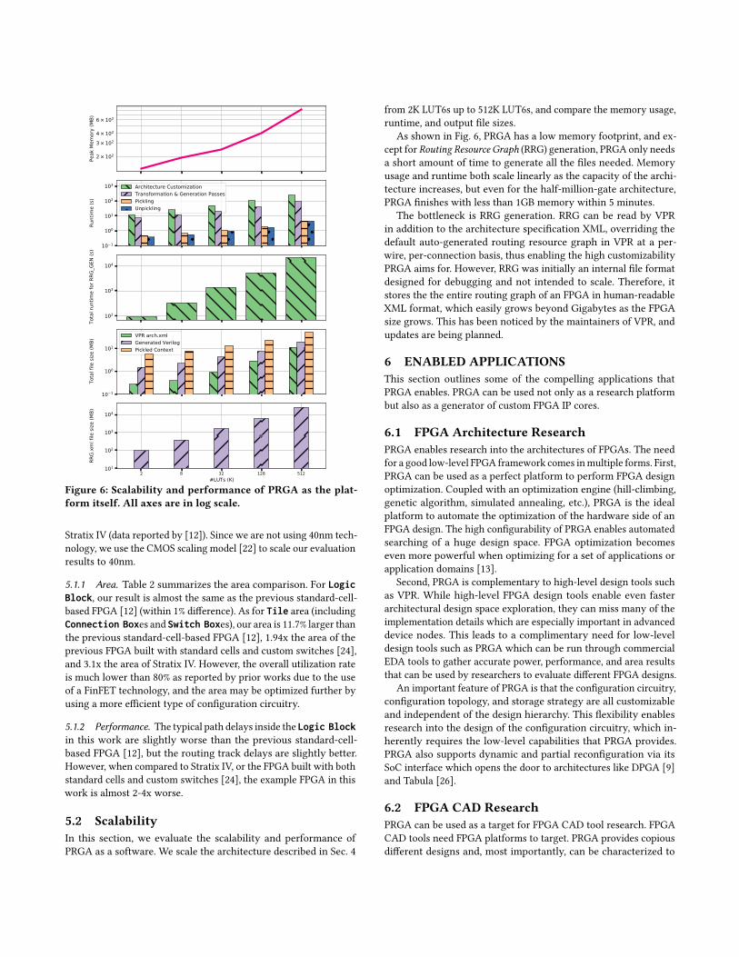
Figure 6: Scalability and performance of PRGA as the plat-form itself. All axes are in log scale.
Stratix IV (data reported by [12]). Since we are not using 40nm tech-nology, we use the CMOS scaling model [22] to scale our evaluationresults to 40nm.
5.1.1 Area. Table 2 summarizes the area comparison. For LogicBlock, our result is almost the same as the previous standard-cell-based FPGA [12] (within 1% difference). As for Tile area (includingConnection Boxes and Switch Boxes), our area is 11.7% larger thanthe previous standard-cell-based FPGA [12], 1.94x the area of theprevious FPGA built with standard cells and custom switches [24],and 3.1x the area of Stratix IV. However, the overall utilization rateis much lower than 80% as reported by prior works due to the useof a FinFET technology, and the area may be optimized further byusing a more efficient type of configuration circuitry.
5.1.2 Performance. The typical path delays inside the Logic Blockin this work are slightly worse than the previous standard-cell-based FPGA [12], but the routing track delays are slightly better.However, when compared to Stratix IV, or the FPGA built with bothstandard cells and custom switches [24], the example FPGA in thiswork is almost 2-4x worse.
5.2 ScalabilityIn this section, we evaluate the scalability and performance ofPRGA as a software. We scale the architecture described in Sec. 4
from 2K LUT6s up to 512K LUT6s, and compare the memory usage,runtime, and output file sizes.
As shown in Fig. 6, PRGA has a low memory footprint, and ex-cept for Routing Resource Graph (RRG) generation, PRGA only needsa short amount of time to generate all the files needed. Memoryusage and runtime both scale linearly as the capacity of the archi-tecture increases, but even for the half-million-gate architecture,PRGA finishes with less than 1GB memory within 5 minutes.
The bottleneck is RRG generation. RRG can be read by VPRin addition to the architecture specification XML, overriding thedefault auto-generated routing resource graph in VPR at a per-wire, per-connection basis, thus enabling the high customizabilityPRGA aims for. However, RRG was initially an internal file formatdesigned for debugging and not intended to scale. Therefore, itstores the the entire routing graph of an FPGA in human-readableXML format, which easily grows beyond Gigabytes as the FPGAsize grows. This has been noticed by the maintainers of VPR, andupdates are being planned.
6 ENABLED APPLICATIONSThis section outlines some of the compelling applications thatPRGA enables. PRGA can be used not only as a research platformbut also as a generator of custom FPGA IP cores.
6.1 FPGA Architecture ResearchPRGA enables research into the architectures of FPGAs. The needfor a good low-level FPGA framework comes inmultiple forms. First,PRGA can be used as a perfect platform to perform FPGA designoptimization. Coupled with an optimization engine (hill-climbing,genetic algorithm, simulated annealing, etc.), PRGA is the idealplatform to automate the optimization of the hardware side of anFPGA design. The high configurability of PRGA enables automatedsearching of a huge design space. FPGA optimization becomeseven more powerful when optimizing for a set of applications orapplication domains [13].
Second, PRGA is complementary to high-level design tools suchas VPR. While high-level FPGA design tools enable even fasterarchitectural design space exploration, they can miss many of theimplementation details which are especially important in advanceddevice nodes. This leads to a complimentary need for low-leveldesign tools such as PRGA which can be run through commercialEDA tools to gather accurate power, performance, and area resultsthat can be used by researchers to evaluate different FPGA designs.
An important feature of PRGA is that the configuration circuitry,configuration topology, and storage strategy are all customizableand independent of the design hierarchy. This flexibility enablesresearch into the design of the configuration circuitry, which in-herently requires the low-level capabilities that PRGA provides.PRGA also supports dynamic and partial reconfiguration via itsSoC interface which opens the door to architectures like DPGA [9]and Tabula [26].
6.2 FPGA CAD ResearchPRGA can be used as a target for FPGA CAD tool research. FPGACAD tools need FPGA platforms to target. PRGA provides copiousdifferent designs and, most importantly, can be characterized to

Project [17] [14] [12] [24] This workStd. Cells ✓ ✓ ✓ ✓ ✓
Custom Cells ✗ ✗ ✗ ✓ ✓
Hetero. Blocks 1 ✗ ✗ ✓ ✓ ✓
Custom Config. ✗ ✗ ✗ ✓2 ✓
Split SB/CB ✗ ✗ ✗ ✗ ✓
Custom Hier. 3 ✗ ✗ ✗ ✗ ✓
Open-Source ✓ ✗ ✗ ✓ ✓1 Support for tall/wide blocks.2 Configuration pins may be exposed for manual connection; No bitstream generation
or RTL support.3 Customizable hierarchy of generated RTL.
Table 4: Taxonomy of FPGA Prototyping Works
provide area, timing, and energy information to feed the FPGACAD tools.
Beyond CAD tools for FPGAs, PRGA is also a good candidatefor being a test design for the greater ASIC CAD tool researcharea. By providing large and parameterized designs, PRGA can beused as a parameterizable benchmark to test chip-design CAD tools.PRGA has already been used as a test case for some emerging opensource CAD tools.
6.3 SoC IntegrationPRGA is not only a research platform. It generates FPGA fabricsthat can be implemented in chips. One of the most promising usecases where free (open-source) or customized FPGAs are desirableis as an embedded FPGA in a System on Chip (SoC). SoCs are be-coming increasingly heterogeneous, and it is difficult to alwaysknow what functionality is needed in an SoC before fabrication.Likewise, applications are evolving faster than ASIC design cycles,pushing more designs to reconfigurable hardware. This has createda growing need for embedded FPGAs [3]. Unlike commercial em-bedded FPGA providers (e.g., Achronix, Flex Logix, QuickLogic)which require licensing fees, PRGA’s open-source nature providesan opportunity to add embedded FPGA functionality without IPlicensing cost. This can be especially impactful in two use cases (1)when only a very small amount of FPGA resources are needed or (2)when the embedded FPGA functionality is needed in low-budgetor academic designs.
7 RELATEDWORKIn this section, we qualitatively compare PRGA with other FPGAprototyping works. Table 4 summarizes the key differences betweenthis work and previous works.
Archipelago [17] is the first open-source project for designingstandard-cell-based FPGAs. It is developed in Chisel [2] and coarselyparameterized, providing limited customizability. It uses an earlyversion of VTR for bitstream generation. Various designs gener-ated by Archipelago were placed and routed using a 65nm processtechnology. Unfortunately, the project is no longer maintained.
There are two [12, 14] successful, standard-cell-based FPGAsbuilt with commercial EDA tools. Based on the VPR/VTR series [18],these projects provide independent data points in the design space,but are not open sourced as publicly available research tools.
OpenFPGA [24] is another open-source FPGA prototyping frame-work that is well-maintained and actively developed. OpenFPGA is
capable of generating synthesizable RTL from an extended XMLschema based on the VTR architecture description file format. MostVTR features are supported, including heterogeneous blocks, multi-modal primitives, carrychains, BRAMs, and so on. In addition, user-defined components and custom cells are also supported. The majordifferences between PRGA and OpenFPGA are the followings:
(1) Currently, OpenFPGA can only generate RTL in a fixed hier-archy: Top-level array → logic and IO blocks, routing boxes→ programmable switches and primitives. PRGA providesmore customizability in module hierarchy and RTL genera-tion, which not only enables more diverse ASIC implemen-tation strategies but also improves scalability.
(2) OpenFPGA is developed on top of VTR [18] and tightly inte-grated with the VTR codebase. PRGA is instead decoupledfrom VTR and uses VTR only as an open-source FPGA place-and-route tool. This decoupling, along with the modularizedworkflow, greatly reduces the bar for PRGA users to cus-tomize and extend the framework, and allows them to focuson their interested part.
(3) OpenFPGA currently supports 4 types of configuration cir-cuitry: chain-based, frame-based, memory-banked, and flat-tened, in which the last one exposes all configuration bits asports of the RTL modules, enabling custom configuration cir-cuitry with limited support for bitstream generation. PRGAallows users to directly modify RTL generation, and providesvarious levels of support for bitstream generation.
8 CONCLUSIONIn conclusion, PRGA is a great platform for building custom FP-GAs. Whether it be enabling researchers or SoC chip builders, theopen-source nature, easy-to-use design, and high configurabilitymake it an excellent low-level FPGA framework in a post-Moore’sLaw world. By providing full Verilog RTL of all of the generateddesigns, area and performance can be modeled with ultimate ac-curacy. PRGA is scalable and provides reasonable runtimes evenfor large designs (an important consideration for commercial use).PRGA provides comparable area and timing delay as other projectsbuilt out of the same technology (standard-cell-based FPGAs). Welook forward to many years of supporting PRGA and expect it toserve as the basis for FPGA research and FPGA designs for yearsto come.
9 ACKNOWLEDGEMENTSWe want to thank our colleagues from the Princeton Parallel Group,especially Ting-Jung Chang, and Fei Gao, for their help with theASIC backend flow. This material is based on research sponsoredby the NSF under Grant No. CCF-1453112, Air Force Research Lab-oratory (AFRL) and Defense Advanced Research Projects Agency(DARPA) under agreement No. FA8650-18-2-7852. The U.S. Govern-ment is authorized to reproduce and distribute reprints for Govern-mental purposes notwithstanding any copyright notation thereon.The views and conclusions contained herein are those of the au-thors and should not be interpreted as necessarily representing theofficial policies or endorsements, either expressed or implied, of AirForce Research Laboratory (AFRL) and Defense Advanced ResearchProjects Agency (DARPA), the NSF, or the U.S. Government.

REFERENCES[1] Amazon. 2020. Amazon EC2 F1 Instances. https://aws.amazon.com/ec2/instance-
types/f1/[2] Jonathan Bachrach, Huy Vo, Brian Richards, Yunsup Lee, Andrew Waterman,
Rimas Avižienis, John Wawrzynek, and Krste Asanović. 2012. Chisel: Construct-ing Hardware in a Scala Embedded Language. In Proceedings of the 49th AnnualDesign Automation Conference (DAC ’12). Association for Computing Machinery,New York, NY, USA, 1216–1225. https://doi.org/10.1145/2228360.2228584
[3] Brian Bailey. 2019. The Case For Embedded FPGAs Strengthens And Widens.https://semiengineering.com/embedded-fpga-becomes-a-viable-option/
[4] Vaughn Betz. 2000. Architecture and CAD for Speed and Area Optimization ofFPGAs. Ph.D. Dissertation. University of Toronto.
[5] Adrian M. Caulfield, Eric S. Chung, Andrew Putnam, Hari Angepat, JeremyFowers, Michael Haselman, Stephen Heil, Matt Humphrey, Puneet Kaur, Joo-Young Kim, Daniel Lo, Todd Massengill, Kalin Ovtcharov, Michael Papamichael,Lisa Woods, Sitaram Lanka, Derek Chiou, and Doug Burger. 2016. A Cloud-ScaleAcceleration Architecture. In The 49th Annual IEEE/ACM International Symposiumon Microarchitecture (MICRO-49). IEEE Press, Article 7, 13 pages.
[6] Yao-Wen Chang, D. F. Wong, and C. K. Wong. 1996. Universal Switch Modulesfor FPGA Design. ACM Trans. Des. Autom. Electron. Syst. 1, 1 (Jan. 1996), 80–101.https://doi.org/10.1145/225871.225886
[7] Paul Chow, Soon Ong Seo, Jonathan Rose, Kevin Chung, and P Gerard. 1999. TheDesign of an SRAM-Based Field-Programmable Gate Array — Part I : Architecture.7, 2 (1999), 191–197.
[8] Eric S. Chung, Peter A. Milder, James C. Hoe, and Ken Mai. 2010. Single-chipHeterogeneous Computing: Does the Future Include Custom Logic, FPGAs, andGPGPUs? Proceedings of the Annual International Symposium onMicroarchitecture,MICRO (2010), 225–236. https://doi.org/10.1109/MICRO.2010.36
[9] André DeHon. 1996. DPGA Utilization and Application. In Proceedings of the1996 ACM Fourth International Symposium on Field-Programmable Gate Arrays(FPGA ’96). Association for Computing Machinery, New York, NY, USA, 115–121.https://doi.org/10.1145/228370.228387
[10] Brian Gaide, Dinesh Gaitonde, Chirag Ravishankar, and Trevor Bauer. 2019. XilinxAdaptive Compute Acceleration Platform: Versal™ Architecture. In Proceedingsof the 2019 ACM/SIGDA International Symposium on Field-Programmable GateArrays (FPGA ’19). Association for Computing Machinery, New York, NY, USA,84–93. https://doi.org/10.1145/3289602.3293906
[11] Mingyu Gao, Christina Delimitrou, Dimin Niu, Krishna T. Malladi, HongzhongZheng, Bob Brennan, and Christos Kozyrakis. 2016. DRAF: A Low-Power DRAM-Based Reconfigurable Acceleration Fabric. SIGARCH Comput. Archit. News 44, 3,506–518. https://doi.org/10.1145/3007787.3001191
[12] Brett Grady and Jason H. Anderson. 2018. Synthesizable Heterogeneous FPGAFabrics. In 2018 International Conference on Field-Programmable Technology (FPT).222–229.
[13] Mark Hammerquist and Roman Lysecky. 2008. Design Space Exploration forApplication Specific FPGAs in System-on-Chip Designs. In 2008 IEEE International
SOC Conference. 279–282.[14] Jin Hee Kim and Jason H. Anderson. 2015. Synthesizable FPGA Fabrics Targetable
by the Verilog-to-Routing (VTR) CAD Flow. In 25th International Conference onField Programmable Logic and Applications, FPL 2015. https://doi.org/10.1109/FPL.2015.7293955
[15] Ang Li, Ting-Jung Chang, and David Wentzlaff. 2020. Automated Design ofFPGAs Facilitated by Cycle-Free Routing. In 2020 30th International Conferenceon Field-Programmable Logic and Applications (FPL). 208–213. https://doi.org/10.1109/FPL50879.2020.00042
[16] Ting-Jung Lin, Wei Zhang, and Niraj K Jha. 2012. FPGA Based on 10T Low-PowerSRAMs. 20, 11 (2012), 2151–2156.
[17] Hao Jun Liu. 2014. Archipelago - An Open Source FPGA with Toolflow Support.Master’s thesis. University of Toronto.
[18] Jason Luu, Jeffrey Goeders, Michael Wainberg, Andrew Somerville, Thien Yu,Konstantin Nasartschuk, Miad Nasr, Sen Wang, Tim Liu, Nooruddin Ahmed,Kenneth B. Kent, Jason Anderson, Jonathan Rose, and Vaughn Betz. 2014. VTR7.0: Next Generation Architecture and CAD System for FPGAs. ACM Trans.Reconfigurable Technol. Syst. 7, 2, Article 6 (July 2014), 30 pages. https://doi.org/10.1145/2617593
[19] Gordon E. Moore. 1965. Cramming More Components Onto Integrated Circuits.Electronics (April 1965).
[20] Duncan J. M. Moss, Eriko Nurvitadhi, Jaewoong Sim, Asit Mishra, Debbie Marr,Suchit Subhaschandra, and Philip H. W. Leong. 2017. High Performance BinaryNeural Networks on The Xeon+FPGA™ Platform. In 2017 27th InternationalConference on Field Programmable Logic and Applications (FPL). 1–4.
[21] Kevin E. Murray, Oleg Petelin, Sheng Zhong, Jia Min Wang, Mohamed Eldafrawy,Jean-Philippe Legault, Eugene Sha, Aaron G. Graham, Jean Wu, Matthew J. P.Walker, Hanqing Zeng, Panagiotis Patros, Jason Luu, Kenneth B. Kent, andVaughn Betz. 2020. VTR 8: High-Performance CAD and Customizable FPGAArchitecture Modelling. ACM Trans. Reconfigurable Technol. Syst. 13, 2, Article 9(May 2020), 55 pages. https://doi.org/10.1145/3388617
[22] Aaron Stillmaker and Bevan Baas. 2017. Scaling Equations for the AccuratePrediction of CMOS Device Performance from 180nm to 7nm. Integration, theVLSI Journal 58, January (2017), 74–81. https://doi.org/10.1016/j.vlsi.2017.02.002
[23] SymbiFlow. 2020. FPGA ASM (FASM). https://fasm.readthedocs.io/en/latest/[24] Xifan Tang, Edouard Giacomin, Aurélien Alacchi, Baudouin Chauviere, and
Pierre-Emmanuel Gaillardon. 2019. OpenFPGA: An Opensource FrameworkEnabling Rapid Prototyping of Customizable FPGAs. In 2019 29th InternationalConference on Field Programmable Logic and Applications (FPL). 367–374. https://doi.org/10.1109/FPL.2019.00065
[25] The Pallets Projects. 2020. Jinja. https://palletsprojects.com/p/jinja/[26] Tom R. Halfhill. 2010. Tabula’s Time Machine. Microprocessor Report.[27] Steven J.E. Wilton. 1997. Architectures and Algorithms for Field-Programmable
Gate Arrays with Embedded Memory. Ph.D. Dissertation. University of Toronto.[28] Clifford Wolf. 2020. Yosys Open SYnthesis Suite. http://www.clifford.at/yosys/.[29] Xilinx. 2020. Zynq-7000 SoC. https://www.xilinx.com/products/silicon-devices/
soc/zynq-7000.html