Embed Size (px)
Citation preview
1
Creating Antennas by Photosintering Silver Nanoparticle Ink on Paper
Prepared by:
Sierra Rasmussen
Faculty Advisors:
Dr. Grant Crawford REU Site Director, Department of Materials and Metallurgical Engineering
Dr. Jon Kellar Professor, Department of Materials and Metallurgical Engineering
Dr. William Cross
Associate Professor, Department of Materials and Metallurgical Engineering
Dr. Alfred Boysen
Professor, Department of Humanities
Program Information: National Science Foundation
Grant #EEC-1263343
Research Experience for Undergraduates Summer 2013
South Dakota School of Mines & Technology 501 E. Saint Joseph Street
Rapid City, SD 57701

2
TABLE OF CONTENTS
Abstract ................................................................................................................................................... 3
Introduction ............................................................................................................................................. 4
Broader Impact ........................................................................................................................................ 4
Procedure ................................................................................................................................................ 4
Materials ..................................................................................................................................... 4
Equipment .................................................................................................................................. 5
Silver Nanoparticle Synthesis ...................................................................................................... 5
Ink Preparation ........................................................................................................................... 5
Printing ....................................................................................................................................... 6
Sintering ..................................................................................................................................... 6
MicroXCT .................................................................................................................................. 7
Conductivity Measurements ........................................................................................................ 7
Antenna ...................................................................................................................................... 7
Results .................................................................................................................................................... 8
Photosintering Effects on Printed Silver ...................................................................................... 8
MicroXCT ................................................................................................................................ 14
Conductivity ............................................................................................................................. 16
Antenna Functionality ............................................................................................................... 17
Discussion ............................................................................................................................................. 20
Conclusion ............................................................................................................................................ 21
References............................................................................................................................................. 22
Acknowledgments ................................................................................................................................. 23
3
Abstract
Silver nanoparticles are a rather novel material with unique optical and electronic properties.
Silver nanoparticles can be mixed into an ink formulation and printed onto a substrate. When the silver
particles in the ink are sintered, they can conduct a charge, allowing their use in printed electronics such
as antennas. However, thermal sintering is generally a high-temperature process and can damage
substrates that are sensitive to heat. The purpose of this research is to determine whether it is possible to
use silver nanoparticles to print a quick-response code on paper that can function as an antenna when the
particles are photonically sintered to create continuous layers of silver.
It was found that photonic sintering does have the ability to sinter silver nanoparticle ink on
paper, and the sintered particles had conductivity ranging from .527-1.5 /Ωm, which is sufficient for
antenna applications. However, the ink seems to have poor adhesion to the paper substrate and further
study will be needed to determine a solution to this.
4
Introduction
Silver nanoparticle ink can be made by suspending silver nanoparticles capped with decanoic acid
in toluene [1]. When printed onto a substrate and fully sintered, the resulting films can be used in
electronics applications. However, the sintering method typically used, thermal sintering, can easily
damage heat-sensitive substrates, such as paper.
To solve this problem, photonic sintering may be used. Photonic sintering is a type of thermal
processing that uses pulses of high-intensity white light to sinter materials [2]. Since this process only
uses light, photonic sintering’s low operating temperature would help to avoid damaging the substrate
during the sintering process [3, 2]. The purpose of this research is to determine whether using photonic
sintering to cure silver nanoparticle ink would attain sufficient conductivity with minimal substrate
deterioration.
Broader Impact
Thermal curing often takes significant lengths of time to complete. Replacing thermal sintering
with photonic sintering would significantly decrease the amount of time needed, allowing for faster
production, and quite possibly, lower energy costs.
Procedure
Materials
AgNO3 (12.74 g)
n-Butylamine (25 mL)
Decanoic acid (6 g)
NaBH4 (2.84 g)
Toluene (33 mL)
5
α-terpineol (200 μL)
Boise brand, 92 bright, 20 lb. 8.5”x11” printer paper
Southworth brand Resume paper, white, 100% cotton, 24 lb. (90 g/m2)
Equipment
Optomec M3D printer
Novacentrix Pulseforge PCS-1100
Xradia brand MicroXCT-400
Materials Development Corporation CSM/WIN System 1398-906
Signatone 1160 Series Probe Station
Silver Nanoparticle Synthesis
Silver nitrate (12.74 g) was added to n-butyl amine (25 mL) and stirred with a magnetic stir bar at
400 rpm. The decanoic acid (6 g) was mixed and dissolved in toluene (23 mL), and then added to the
silver nitrate and n-butylamine solution while continuing to stir at 400 rpm. To reduce the potential of the
solution, sodium borohydride (2.84 g) was added, and the solution was heated to approximately 80°C, and
refluxed for one hour. When the refluxing was finished, the solution was allowed to return to room
temperature and left for at least eight hours.
To clean the nanoparticles from the remaining solution, a mixture of acetone (250 mL) and
methanol (250 mL) was added and filtered through a glass filter. Next, another 250 mL of acetone was
added and filtered, followed by another 250 mL of methanol. When the filtering was complete, the
particles were left to dry in closed Petri dishes overnight.
Ink Preparation
The particles were gently ground in a mortar and pestle and added to a vial and toluene (10 mL)
was added. The vial was capped and shaken vigorously to redisperse the nanoparticles. The vial was then
6
put in a vortex mixer for 30 minutes at 3000 rpm, and then sonicated for 30 minutes to help more
thoroughly redisperse the nanoparticles. The vial was then vortex mixed and sonicated again with the
same parameters, and then centrifuged at 6000 rpm for 90 minutes to remove agglomerates. The ink was
removed from the centrifuge tubes using a pipette, being careful not to pick up the particles that settled
during centrifuging. To determine the weight percent of silver nanoparticles, a glass vial was weighed,
100 μL were deposited inside and evaporated, and the vial was weighed again.
Printing
The final ink was printed using an Optomec M3D printer with a 300 μm orifice. Before printing,
2 mL of silver nanoparticle ink previously prepared was deposited in a glass vial, and approximately 200
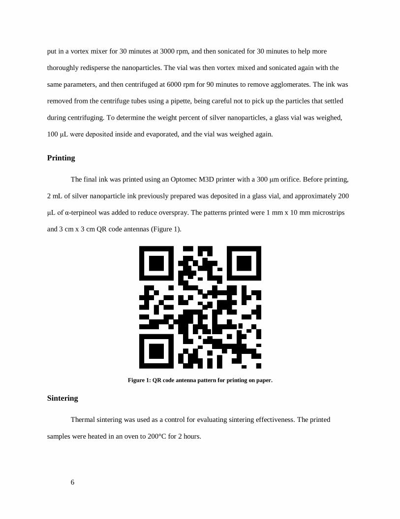
μL of α-terpineol was added to reduce overspray. The patterns printed were 1 mm x 10 mm microstrips
and 3 cm x 3 cm QR code antennas (Figure 1).
Figure 1: QR code antenna pattern for printing on paper.
Sintering
Thermal sintering was used as a control for evaluating sintering effectiveness. The printed
samples were heated in an oven to 200°C for 2 hours.
7
To photonically sinter the silver nanoparticles, a Novacentrix Pulseforge PCS-1100 was used.
The silver was sintered using a white lamp, using settings of 800-1200 V for 500-900 μs. 1200 V and 900
μs were used as maxima for the sintering parameters, as they were most effective in sintering silver
nanoparticles of a larger size [3].
MicroXCT
MicroXCT images were created using a MicroXCT-400 manufactured by Xradia. Source settings
used were 40 kV, 250 μA. Pixel size was 17.8761 μm. 1600 frames were taken of the sample, rotated
180°, and the exposure time for each frame was 8.0 seconds.
Conductivity Measurements
Sheet resistance was measured using a Materials Development Corporation CSM/WIN System
1398-906 four point probe measurement system. Other resistance measurements were taken using a
Signatone 1160 Series Probe Station.
Antenna
The QR code antenna pattern used was designed by Mr. Abu Numan-Al-Mobin to resonate at 2.4
GHz. AutoCAD was used to generate the toolpath for printing with Optomec M3D.
An Agilent 8753SE Vector Network Analyzer was used to measure return loss of the antenna in a
custom-built anechoic chamber [4].
8
Results
Photosintering Effects on Printed Silver
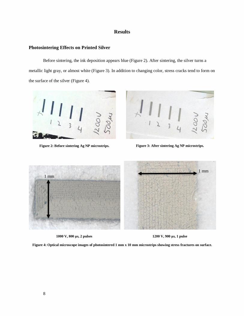
Before sintering, the ink deposition appears blue (Figure 2). After sintering, the silver turns a
metallic light gray, or almost white (Figure 3). In addition to changing color, stress cracks tend to form on
the surface of the silver (Figure 4).
Figure 2: Before sintering Ag NP microstrips.
Figure 3: After sintering Ag NP microstrips.
1000 V, 800 μs, 2 pulses
1200 V, 900 μs, 1 pulse
Figure 4: Optical microscope images of photosintered 1 mm x 10 mm microstrips showing stress fractures on surface.
1 mm
1 mm
9
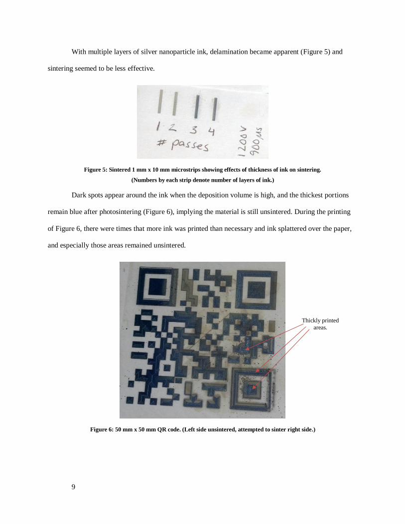
With multiple layers of silver nanoparticle ink, delamination became apparent (Figure 5) and
sintering seemed to be less effective.
Figure 5: Sintered 1 mm x 10 mm microstrips showing effects of thickness of ink on sintering.
(Numbers by each strip denote number of layers of ink.)
Dark spots appear around the ink when the deposition volume is high, and the thickest portions
remain blue after photosintering (Figure 6), implying the material is still unsintered. During the printing
of Figure 6, there were times that more ink was printed than necessary and ink splattered over the paper,
and especially those areas remained unsintered.
Figure 6: 50 mm x 50 mm QR code. (Left side unsintered, attempted to sinter right side.)
Thickly printed
areas.
10
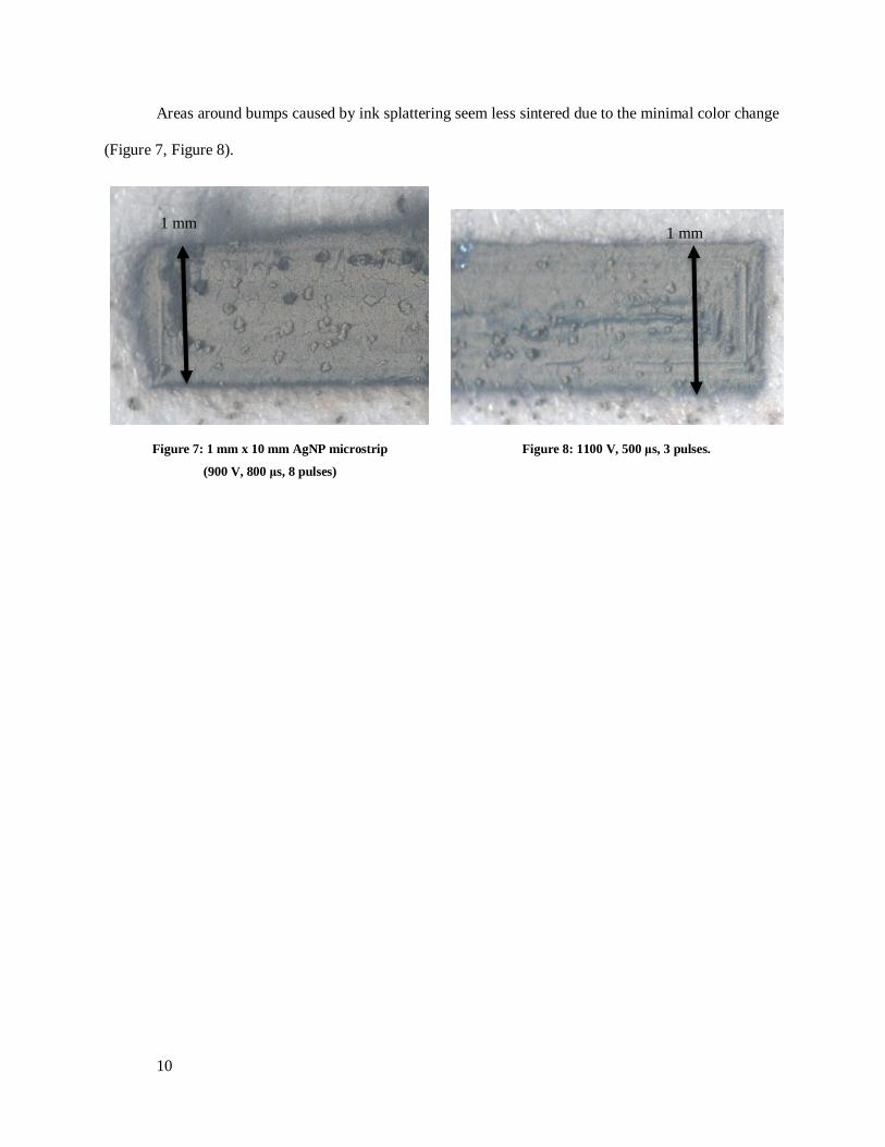
Areas around bumps caused by ink splattering seem less sintered due to the minimal color change
(Figure 7, Figure 8).
Figure 7: 1 mm x 10 mm AgNP microstrip
(900 V, 800 μs, 8 pulses)
Figure 8: 1100 V, 500 μs, 3 pulses.
1 mm 1 mm
11
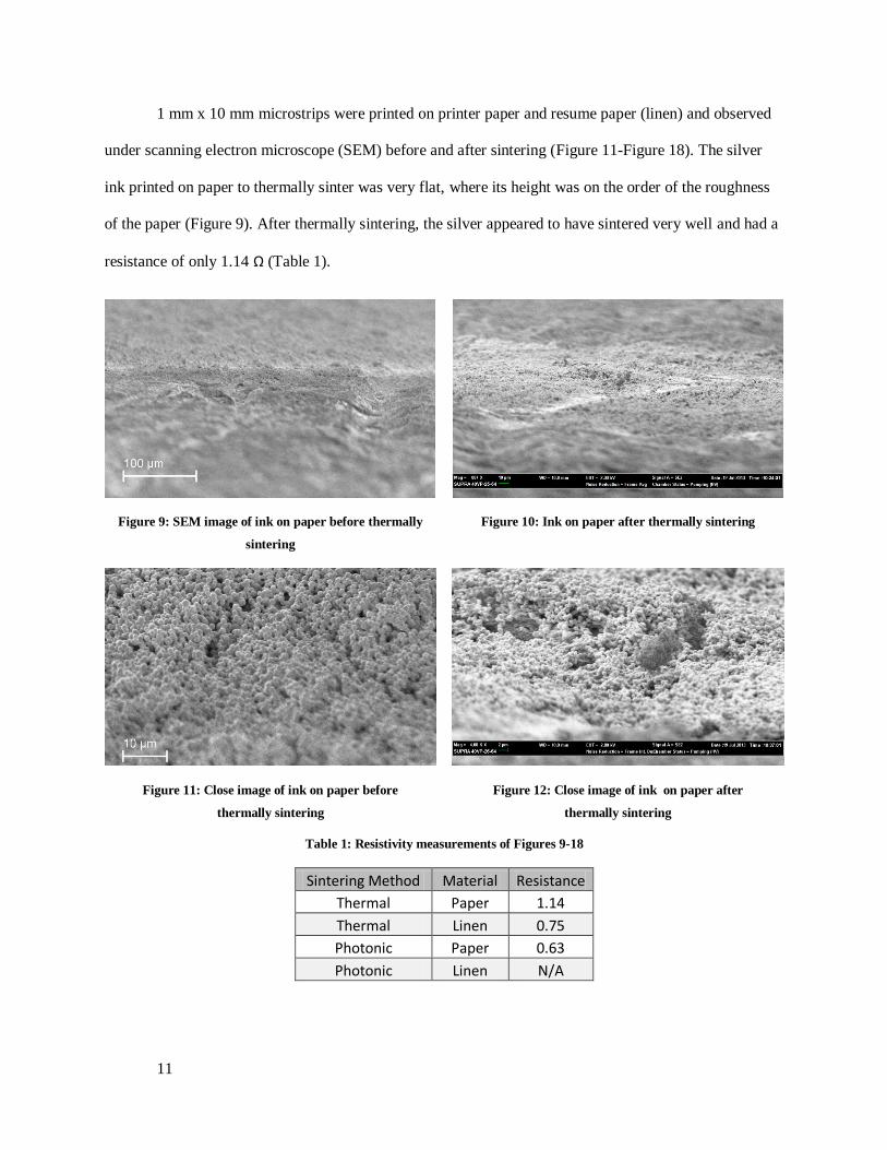
1 mm x 10 mm microstrips were printed on printer paper and resume paper (linen) and observed
under scanning electron microscope (SEM) before and after sintering (Figure 11-Figure 18). The silver
ink printed on paper to thermally sinter was very flat, where its height was on the order of the roughness
of the paper (Figure 9). After thermally sintering, the silver appeared to have sintered very well and had a
resistance of only 1.14 Ω (Table 1).
Figure 9: SEM image of ink on paper before thermally
sintering
Figure 10: Ink on paper after thermally sintering
Figure 11: Close image of ink on paper before
thermally sintering
Figure 12: Close image of ink on paper after
thermally sintering
Table 1: Resistivity measurements of Figures 9-18
Sintering Method Material Resistance
Thermal Paper 1.14
Thermal Linen 0.75
Photonic Paper 0.63
Photonic Linen N/A
12
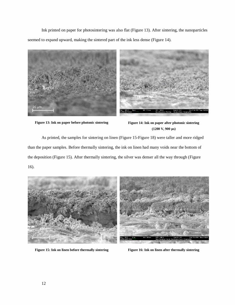
Ink printed on paper for photosintering was also flat (Figure 13). After sintering, the nanoparticles
seemed to expand upward, making the sintered part of the ink less dense (Figure 14).
Figure 13: Ink on paper before photonic sintering
Figure 14: Ink on paper after photonic sintering
(1200 V, 900 μs)
As printed, the samples for sintering on linen (Figure 15-Figure 18) were taller and more ridged
than the paper samples. Before thermally sintering, the ink on linen had many voids near the bottom of
the deposition (Figure 15). After thermally sintering, the silver was denser all the way through (Figure
16).
Figure 15: Ink on linen before thermally sintering
Figure 16: Ink on linen after thermally sintering
13
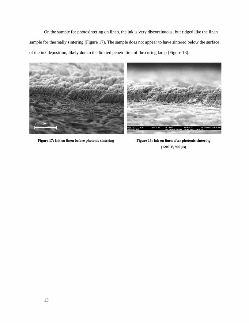
On the sample for photosintering on linen, the ink is very discontinuous, but ridged like the linen
sample for thermally sintering (Figure 17). The sample does not appear to have sintered below the surface
of the ink deposition, likely due to the limited penetration of the curing lamp (Figure 18).
Figure 17: Ink on linen before photonic sintering
Figure 18: Ink on linen after photonic sintering
(1200 V, 900 μs)
14
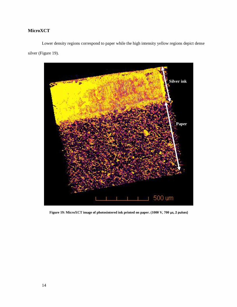
MicroXCT
Lower density regions correspond to paper while the high intensity yellow regions depict dense
silver (Figure 19).
Figure 19: MicroXCT image of photosintered ink printed on paper. (1000 V, 700 μs, 2 pulses)
Silver ink
Paper
15
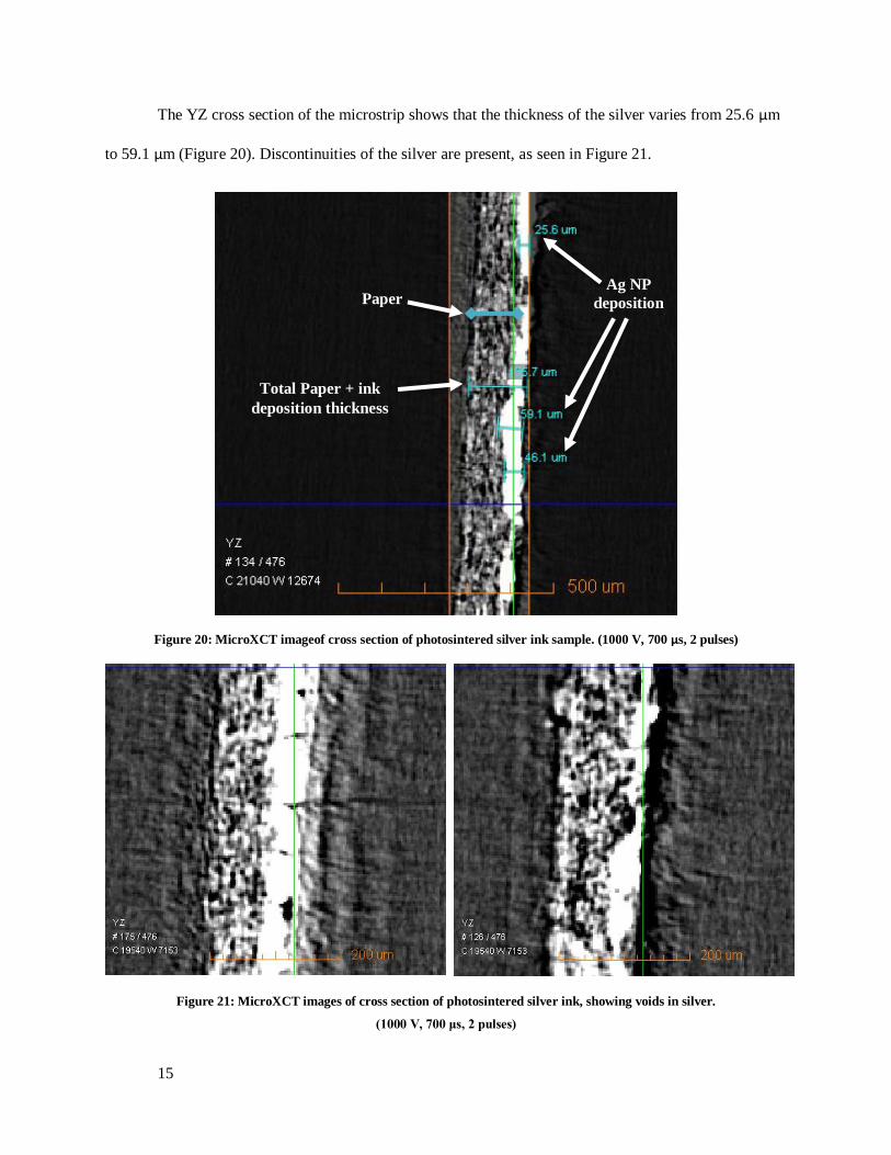
The YZ cross section of the microstrip shows that the thickness of the silver varies from 25.6 μm
to 59.1 μm (Figure 20). Discontinuities of the silver are present, as seen in Figure 21.
Figure 20: MicroXCT imageof cross section of photosintered silver ink sample. (1000 V, 700 μs, 2 pulses)
Figure 21: MicroXCT images of cross section of photosintered silver ink, showing voids in silver.
(1000 V, 700 μs, 2 pulses)
Paper Ag NP
deposition
Total Paper + ink
deposition thickness
16
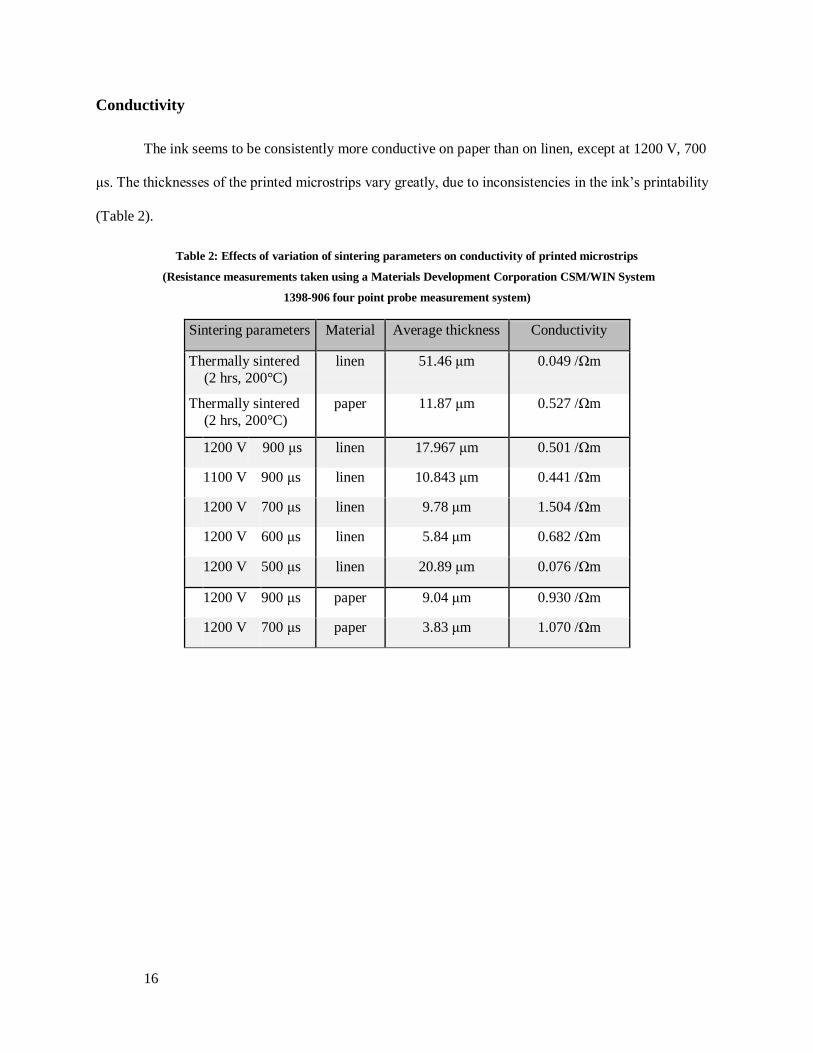
Conductivity
The ink seems to be consistently more conductive on paper than on linen, except at 1200 V, 700
μs. The thicknesses of the printed microstrips vary greatly, due to inconsistencies in the ink’s printability
(Table 2).
Table 2: Effects of variation of sintering parameters on conductivity of printed microstrips
(Resistance measurements taken using a Materials Development Corporation CSM/WIN System
1398-906 four point probe measurement system)
Sintering parameters Material Average thickness Conductivity
Thermally sintered
(2 hrs, 200°C)
linen 51.46 μm 0.049 /Ωm
Thermally sintered
(2 hrs, 200°C)
paper 11.87 μm 0.527 /Ωm
1200 V 900 μs linen 17.967 μm 0.501 /Ωm
1100 V 900 μs linen 10.843 μm 0.441 /Ωm
1200 V 700 μs linen 9.78 μm 1.504 /Ωm
1200 V 600 μs linen 5.84 μm 0.682 /Ωm
1200 V 500 μs linen 20.89 μm 0.076 /Ωm
1200 V 900 μs paper 9.04 μm 0.930 /Ωm
1200 V 700 μs paper 3.83 μm 1.070 /Ωm
17
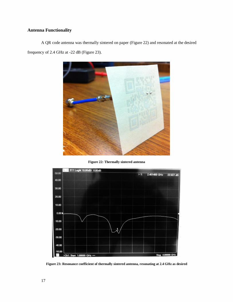
Antenna Functionality
A QR code antenna was thermally sintered on paper (Figure 22) and resonated at the desired
frequency of 2.4 GHz at -22 dB (Figure 23).
Figure 22: Thermally sintered antenna
Figure 23: Resonance coefficient of thermally sintered antenna, resonating at 2.4 GHz as desired
18
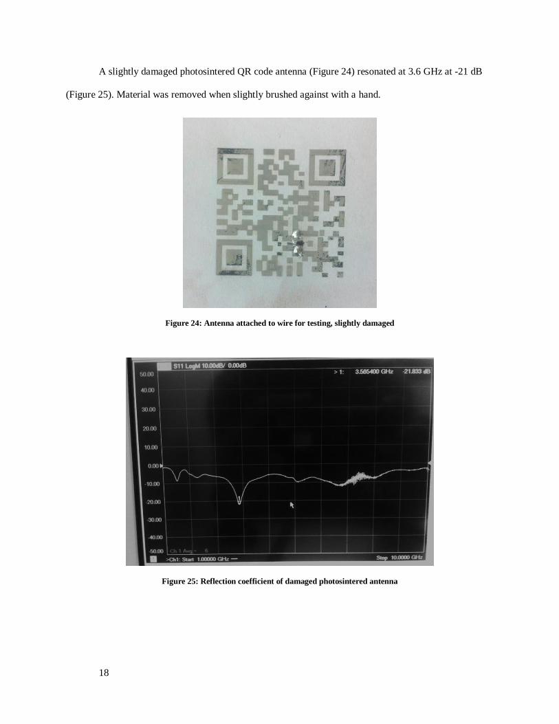
A slightly damaged photosintered QR code antenna (Figure 24) resonated at 3.6 GHz at -21 dB
(Figure 25). Material was removed when slightly brushed against with a hand.
Figure 24: Antenna attached to wire for testing, slightly damaged
Figure 25: Reflection coefficient of damaged photosintered antenna
19
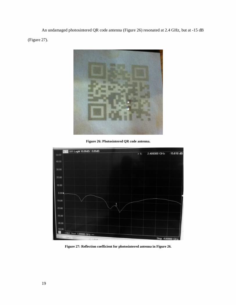
An undamaged photosintered QR code antenna (Figure 26) resonated at 2.4 GHz, but at -15 dB
(Figure 27).
Figure 26: Photosintered QR code antenna.
Figure 27: Reflection coefficient for photosintered antenna in Figure 26.
20
Discussion
Photonic sintering was effective in obtaining sufficient conductivity of the silver nanoparticle ink.
As particle size decreases, melting temperature also decreases [5, 6], implying that less energy is needed
for sintering to occur between silver nanoparticles than for bulk silver. This makes photonic sintering an
attractive method of creating conductive macrostructured silver from silver nanoparticle ink.
The surface delamination (Figure 5) could have been due to high thermal dissipation forcing
silver layers apart, multiple stress cracks caused by the high heating and cooling rates, or large amounts of
outgassing from photonic curing removing the capping agent decanoic acid and residual solvent toluene.
Conductivity seemed to decrease with thicker ink depositions and less sintering seemed apparent,
possibly due to delamination of the sintered surface material.
Paper also appeared to have a large capillary force on toluene, and swelled slightly in its
presence. This swelling could skew actual ink thickness data if swelling was limited to beneath the
deposition. After being exposed to toluene and being photocured, paper did not seem to discolor.
However, discoloration was obvious with trace amounts of silver present (Figure 6).
Conductivity could be affected by cracks (Figure 4) and discontinuities (Figure 21) in the sintered
silver film. Conductivity could also be affected by the depth of the sintered material.
The adhesion of the ink to paper seems poor after photonic sintering; light brushing against any
surface seems to remove material (Figure 24). This may be due to incomplete sintering from the low
penetration of the lamp. The photonic light penetrates up to approximately 5 μm, suggesting that any
sintering deeper than this distance could be due to thermal conduction of the ink [3]. This loss of material
affects the conductive area of the antenna, and consequently, the frequencies at which it resonates (Figure
24). The thickness of the ink is not crucial to the functionality of the antenna, although the requested
minimum thickness of ink deposition was approximately 5μm. The surface conductivity is the main
21
concern for the functionality of the antenna, as only the surface “skin” of the deposition is important for
resonation.
Conclusion
Photonically sintered silver nanoparticle ink on paper demonstrates sufficient conductivity for
antenna applications, with minimal alteration to the substrate. Also, a QR code antenna that resonated at
2.4 GHz was successfully printed on paper for Wi-Fi application.
For future work, it will be necessary to improve ink adhesion to the substrate. Possible solutions
include a thin polymer coating over the deposition or use of thermally-assisted photosintering to more
thoroughly sinter the underlying material.
22
References
1. Ankireddy, K., Vunnam, S., Kellar, J., & Cross, W. (2013). Highly conductive short chain carboxylic
acid encapsulated silver nanoparticle based inks for direct write technology applications. Journal of
Materials Chemistry C, 1, 572-. doi: 10.1039/c2tc00336h
2. Falat, T., Felba, J., Platek, B., Piasecki, T., Moscicki, A., & Smolarek, A. (2011). Low-temperature,
photonic approach to sintering the ink-jet printed conductive microstructures containing
nano sized silver particles . In 2011 18th European Microelectronics and Packaging
Conference (EMPC), (pp. 1, 4, 12-15). Retrieved from
http://ieeexplore.ieee.org/xpl/freeabs_all.jsp?arnumber=6142409&tag=1&abstractAccess=no&userTy
pe=inst
3. Carter, M., Sears, J., Smith, S., & West, J. (2012). Photonic sintering of silver nanoparticles:
Comparison of experiment and theory. In V. Shatokha (Ed.), Sintering - Methods and Products.
Retrieved from http://www.intechopen.com/books/sintering-methods-andproducts/ photonic-
sintering-of-silver-nanoparticles-comparison-of-experiment-and-theory
4. Anagnostou, D. E., Gheethan, A. A., Amert, A. K., & Whites, K. W. (2010). A direct-write printed
antenna on paper-based organic substrate for flexible displays and WLAN applications. Journal of
Display Technology, 6(11), 558-564.
5. Zhang, M., Efremov, M. Y., Schiettekatte, F., Olson, E. A., Kwan, A. T., Lai, S. L., ... & Allen, L. H.
(2000). Size-dependent melting point depression of nanostructures: Nanocalorimetric
measurements. Physical Review B, 62(15), 10548. doi: 10.1103/PhysRevB.62.10548
6. Sun, J., & Simon, S. L. (2007). The melting behavior of aluminum nanoparticles. Thermochimica
Acta, 463(1), 32-40. doi: 10.1016/j.tca.2007.07.007
23
Acknowledgments
Thanks to the National Science Foundation for providing funding for this research (NSF Grant
#EEC-1263343). Also, special thanks to advisors Dr. Jon Kellar, REU director Dr. Grant Crawford, Dr.
William Cross, James Randle, Dr. Anagnostou, and Dr. Alfred Boysen, graduate students Jacob Petersen,
Abu Numan-Al-Mobin, Jeevan Meruga, and Krishnamraju Ankireddy, and the rest of the REU staff for
their support, assistance, and guidance with this research. The micro-computed tomography equipment
used in this research was purchased through NSF Grant #CMMI-1126848.