Embed Size (px)
Citation preview

Table of contents
1 INTRODUCTION................................................................................................3
1.1 NUMBER SYSTEMS....................................................................................41.2 Base Values....................................................................................................41.3 Decimal Number System...............................................................................41.4 Binary Number system ( Base 2)...................................................................51.5 Octal Base System (Base 8)...........................................................................51.6 Hexadecimal Number System (Base16)........................................................5
2 CONVERTING DECIMAL NUMBERS TO BINARY NUMBERS..............6
2.1 Method 1: Using the remainder theorem.......................................................62.2 Method 2: Using the Binary Exponential Placeholders.................................72.3 CONVERTING DECIMAL FRACTIONS TO BINARY...........................102.4 Converting mixed decimal numbers to binary.............................................112.5 Converting decimal numbers to octal number system.................................132.6 Converting decimal fractions to octal system..............................................132.7 Converting decimal numbers to Hexadecimal number system....................152.8 Converting decimal fractions to hexadecimal number system....................152.9 Converting binary numbers to octal number system....................................162.10 Converting binary numbers to hexadecimal number system.......................17
3 SIGNED FIXED POINT NUMBERS..............................................................18
3.1 Signed magnitude.........................................................................................183.2 Ones Complement........................................................................................183.3 Twos complement........................................................................................193.4 Excess Representation..................................................................................203.5 Gray Code....................................................................................................223.6 Converting a number in Gray to Binary.......................................................223.7 Excess 3 Gray Code.....................................................................................253.8 Range and Precision in Floating Point Numbers.........................................253.9 Representing floating point numbers in the computer.................................26
4 BINARY CODED DECIMAL..........................................................................29
4.1 Representing signed numbers in BCD.........................................................294.2 NINES AND TENS COMPLEMENT.........................................................30
4.2.1 Nines complement (Negative)..............................................................304.2.2 Tens complement (Negative)...............................................................30
5 COMPUTER CODES........................................................................................31
5.1 ASCII (American Standard Code for Information Interchange).................315.2 EBCDIC – (Extended Binary Coded Decimal Information Code).............325.3 UNICODE....................................................................................................33
6 BOOLEAN ALGEBRA.....................................................................................35
6.1 PROPERTIES OF BOOLEAN ALGEBRA................................................356.2 DE MORGAN’S THEOREM......................................................................36
7 LOGIC GATES..................................................................................................38
1

7.1 NOT Logic gate...........................................................................................387.2 The OR Logic Gate......................................................................................397.3 The AND logic gate.....................................................................................407.4 The NOR logic gate.....................................................................................407.5 The NAND logic gate..................................................................................417.6 EXclusive OR (XOR) logic gate..................................................................427.7 EXclusive NOR (XNOR) logic gate............................................................42
8 KARNAUGH MAPS..........................................................................................44
8.1 One variable Karnaugh map.........................................................................448.2 Two variable Karnaugh map........................................................................448.3 The three variable Karnaugh map................................................................458.4 The Four variable Karnaugh map................................................................468.5 Karnaugh Maps Rules for Boolean Functions Simplification.....................468.6 WORKING WITH DON’T CARE CONDITIONS....................................51
9 COMBINATIONAL AND SEQUENTIAL CIRCUITS.................................55
9.1 ADDERS......................................................................................................559.2 FULL ADDER.............................................................................................579.3 REDUCTION OF COMBINATIONAL CIRCUITS...................................599.4 DECODER...................................................................................................619.5 MULTIPLEXER (MUX).............................................................................639.6 DE MULTIPLEXER (DEMUX).................................................................64
10 SEQUENTIAL CIRCUITS...............................................................................65
10.1 Flip Flop Circuits.........................................................................................6510.2 Clocked R S Flip Flop..................................................................................6810.3 JK Flip-flop (Universal Flip-flop)................................................................6910.4 JK Master Slave flip-flop built on NAND gates..........................................7010.5 D flip-flop (Delay Flip-flop)........................................................................7110.6 EDGE TRIGGERED FLIP FLOPS.............................................................7210.7 EXCITATION TABLES.............................................................................7310.8 SEQUENTIAL CIRCUIT EQUATIONS....................................................75
11 DIGITAL COUNTERS.....................................................................................84
11.1 An asynchronous 4 bit Binary Up counter...................................................8511.2 An Asynchronous 4-Bit Down Counter......................................................8611.3 SYNCHRONOUS COUNTERS..................................................................88
12 REGISTERS AND THEIR OPEATIONS.......................................................90
12.1 SHIFT REGISTERS....................................................................................9212.2 SERIAL-IN SERIAL-OUT REGISTER......................................................9212.3 SERIAL-IN PARALLEL-OUT SHIFT REGISTER...................................9312.4 PARALLEL IN- SERIAL –OUT REGISTER............................................94
APPENDICES....................................................................................................95
APPENDIX 1...........................................................................................................95APPENDIX 2...........................................................................................................98
REFERENCES.........................................................................................................101
2
1 INTRODUCTION
Digital Logic Technology has a strong impact in our daily lives. Therefore a course
in Digital Logic Design Concepts becomes a standard requirement for undergraduates
majoring in computer science, physics, electrical engineering as and in mathematics
(for those who do a computer science with mathematics degree).
In this module emphasis is on digital logic design. This book assumes no background
in computers on the part of the reader but a good background in physics and
mathematics is a requirement. Our intention, as authors of this module, is to present a
set of procedures commonly encountered in Digital Logic Design.
Our philosophy as authors of this module is that an introductory course in Digital
Logic Design should establish a strong foundation on the basic principles that are
provided by a more traditional approach to the design of combinational and sequential
circuits before one engages on the use of computer-aided design tools.
Once the basic concepts and principles have been mastered then the use of design
software becomes more meaningful and allows the student to use the design software
more effectively. So this module focuses on the understanding of basic principles of
Digital Logic Design and the application of these principles to the analysis and design
of combinational and sequential logic circuits
3

1.1 NUMBER SYSTEMS
A number system defines a set of values used to represent quantity. We talk about the
number of people attending class, the number of modules taken per student, and also
use numbers to represent grades achieved by students in tests.
Quantifying values and items in relation to each other is helpful for us to make sense
of our environment. The study of number systems is not just limited to computers. We
apply numbers every day, and knowing how numbers work will give us an insight
into how a computer manipulates and stores numbers.
1.2 Base Values
The base value of a number system is the number of different values the set has before
repeating itself. For example, decimal has a base of ten values, 0 to 9.
Decimal = 10 (0 - 9) Binary = 2 (0, 1)
Octal = 8 (0 - 7)
Hexadecimal = 16 (0 - 9, A-F)
We will limit ourselves to the above number base systems.
1.3 Decimal Number System
This number base system is also called denary system and is the most common to us
as human beings as we use it in our daily lives to do calculations and counting. It uses
ten (10) different symbols to represent values. The set values used in decimal are 0 1
2 3 4 5 6 7 8 9 and 0 has the least value and nine has the greatest value. The digit on
the left has the greatest value, whilst the digit on the right has the least value.
4

Although this is the most common number base system in use in our daily lives, the
computers do not use this base for representing data/information.
1.4 Binary Number system ( Base 2)
The binary number system uses two values to represent numbers. The values are, 0
and a 1. These two values have also the interpretations FALSE for a 0 and TRUE for
a 1, LOW for a 0 and HIGH for a 1, OFF for 0 and ON for a 1. Zero (0) has the least
value, and one (1) has the greatest value. The least value is also called the least
significant bit (LSB), the greatest value the most significant bit (MSB)
1.5 Octal Base System (Base 8)
The octal number system uses eight values to represent numbers. The values are 0, 1,
2, 3, 4, 5, 6, 7 with 0 having the least value and seven having the greatest value.
1.6 Hexadecimal Number System (Base16)
The hexadecimal number system uses sixteen values to represent numbers. The values
are, 0 1 2 3 4 5 6 7 8 9 A B C D E F with 0 having the least value and F having the
greatest value.
5

2 CONVERTING DECIMAL NUMBERS TO BINARY NUMBERS
There are a number of ways to convert between decimal and binary.
We will start converting the decimal value 50 to binary using the remainder
theorem also called the division method followed by the Subtraction method.
2.1 Method 1: Using the remainder theorem
Steps
1. Divide the decimal number by 2, and note down the remainder
2. Divide the quotient by 2 and note the remainder
3. Repeat step 2 until the number is no longer divisible by 2
4. Write down the remainder values in reverse order..
Example 1
Convert 15010 to Binary
150 / 2 75 remainder 0 LS B
75 / 2 37 remainder 1
37 / 2 18 remainder 1 18 / 2 9 remainder 0 9 / 2 4 remainder 1 4 / 2 2 remainder 0 2/ 2 1 remainder 0 1 / 2 0 remainder 1 MSB
Thus the binary equivalent is 1001011. This binary number is equivalent to 15010.
We also need to prove that this is correct. To do this, we write the binary number and
give it weights (indices) beginning with 20.
6

For example 17 06 05 14 03 12 11 00
27 x 1 + 26 x 0 + 25 x 0 + 24 x 1 + 23 x 0 + 22 x 1 + 21 x 1+ 20 x 0
128 x 1 + 0 + 0 + 16 + 0 + 0+4+2 = 150
Example 2 Convert 13210 to binary equivalent
132 / 2 66 remainder 0 LSB 66 / 2 33 remainder 0
33 / 2 16 remainder 1
16 / 2 8 remainder 0
8 / 2 4 remainder 0
4 / 2 2 remainder 0
2 / 2 1 remainder 0
1 / 2 0 remainder 1 MSB
Thus the binary equivalent is 10000100
We also proved that this was correct.
1706 05 04 03 12 01 00
128 x 1 + 4 = 132
2.2 Method 2: Using the Binary Exponential Placeholders.
This method uses the binary weighting system and is also sometimes referred to as the
8:4:2:1 approach. Each column represents a power of 2. To make things easy one
must to know the binary exponential holders.
7

Example: Convert 1110 to its binary equivalent.
The highest power of two number nearest to eleven is 3, so 23 is 8
We write 8 4 2 1 1 0 1 1
We ask ourselves the question, can 8 be subtracted from 11? The answer is yes, we
write a one under the column 8. We subtract 8 from 11 and the answer is 3. The
next highest power of two is 4. Ask our selves the question; can 4 be subtracted from
3? Answer is no. Write a zero (o) under column 4. The next highest power of 2 is
two. Ask our selves the question, can two be subtracted from 3. The answer is yes and
we write 1 under column 2. We subtract 2 from 3. The answer is 1. The next highest
power of two is 1. We ask our selves the question; can 1 be subtracted from 1? The
answer is yes, we write a 1under column 1.
So 1110 is equivalent to 10112
Example:
Convert 19710 to binary using Binary Exponential Placeholders
The highest Binary Exponential Placeholders next to 127 is 128, which is 27. If 128
can be subtracted from 128, we write a 1 in column 128, Subtract 128 from 197. The
answer is 69. If 64 can be subtracted from 69, we put a 1 in column in 64. We subtract
64 from 69. The answer is 5. 32 cannot be subtracted from 5. We put a zero (0) in
column 32. Next is column is 8, which cannot be subtracted from 5 and we put a 0 in
column 8. Next is column 4. 4 can be subtracted from 5, so we put a 1 in column 4.
Subtract 4 from 5 and the answer is 1. Next column is 2 and 2 cannot be subtracted
from 1 and we write a 0 in column 2. Next column is 1 and 1 can be subtracted from
1, so we put a 1 in column 1.
8

Positional weight 27 26 25 24 23 22 21 20
Value 128 64 32 16 8 4 2 1
Number 1 1 0 0 0 1 0 1
So we have 1 1 0 0 0 1 0 12 = 19710
We prove this by converting 11000101 back to decimal.
27 x 1+ 26x1+25x 0+24x 0+23x 0 +22x1+21x0+20x1
= 128+64+4++1=197
Advantages of Binary number system are:
- Simple to work with (uses only two symbols i.e. a zero (0) and a one (1);
- Lower power consumption as it uses only two states and
- Easy to convert from binary to octal decimal and hexadecimal number
base systems
Disadvantages binary conversions
Binary numbers are:
- Cumbersome to write down;
-Long strings of 1s and zeros and one can easily make mistakes when dealing
with large numbers;
- Not very meaning to the average user and
-They are understood by computers
Binary table Decimal equivalent
00 0
01 1
9

10 2
11 3
2.3 CONVERTING DECIMAL FRACTIONS TO BINARY
Decimal fractions are converted to binary fractions equivalent using the multiplication
method.
Steps
1. Write down the decimal fraction
2. Multiply the decimal fraction by 2
3. Write down the whole number part
4. Repeat steps 2 and 3 until the degree of accuracy has been achieved.
5. Write down the whole numbers in the order you produced them.
Note that when converting decimal fractions to their binary equivalents, we should do
this to a given degree of accuracy, i.e. the number of decimal points places that are
needed. When using binary fractions it is recommended to use a less number of
decimal places as the fractions become very inaccurate as the number of decimal
points increases.
Example:
Convert 0.12510 to binary equivalent
.125 x 2 = 0.250 whole number part = 0 MSB
.250 x 2 = 0.500 whole number part = 0
.500 x 2 = 1.000 whole number part = 1 LSB
Proof:
0-1 0-2 1-3
2-1 x 0 +2-2 x 0 +2-3 x1
10

½1 x 0 + ½2 x 0 + ½3 x 1
= 1/8 = 0.125
Example:
Convert 0.25510 to binary equivalent
0.255 x 2 = .510 whole number part = 0 MSB
0.510 x 2 = 1.020 whole number part = 1
0.020 x 2 = .040 whole number part = 0
0-1 1-2 0-3
2-1 x 0 + 2-2 x 1 + 2-3 x 0
= ½2 = ¼ = 0.250
This is what I meant when I said (above) when the number of binary point places
increases the fractions become inaccurate. As can be observed from the above
example 0.255 when converted to binary fraction converts to 0.250 and not to 0.255.
The major disadvantage of converting decimal fractions to binary fractions is that
some precision can be lost in the process of conversion, for example not all
terminating decimal fractions have a terminating binary equivalent, for example 0.210
becomes non-terminating binary fraction.
2.4 Converting mixed decimal numbers to binary
Steps
1 Use the remainder theorem to convert the decimal number to binary
2 Use the multiplication method to convert the decimal fraction to binary fraction
3 Write the binary integer part, followed by a period and then the fraction part.
11

Example:
Convert 132.12510 to binary equivalent
We convert the whole number (integer) part using the division method
132 / 2 66 remainder 0 LSB
66 / 2 33 remainder 0
33 / 2 16 remainder 1
16 / 2 8 remainder 0 8 / 2 4 remainder 0 4 / 2 2 remainder 0
2 / 2 1 remainder 0 1 / 2 0 remainder 1 MSB
Thus the binary equivalent is 10000100
We also prove that this is correct by converting back to decimal.
1706 05 04 03 12 01 00
128 x 1 + 4 = 132
We convert the fraction part (.12510) to binary equivalent using the multiplication
method
.125 x 2 = 0.250 whole number part = 0 MSB
.250 x 2 = 0.500 whole number part = 0
.500 x 2 = 1.000 whole number part = 1 LSB
Proof:
0-1 0-2 1-3
2-1 x 0 +2-2 x 0 +2-3 x 1
12

½1 x 0 + ½2 x 0 + ½3 x 1
= 1/8 = 0.125
So 10000100.0012 is equivalent to 132.12510
2.5 Converting decimal numbers to octal number system
Steps
1. Divide the decimal number by 8 and note down the remainder
2. Divide what's left (quotient) by 8 and note the remainder
3. Repeat step 2 until the number is no longer divisible by 8
4. Write down the remainders values in reverse order.
Example:
Problem: Convert 17610 in octal to decimal
176 / 8 = 22 remainder 0 LSB 22/ 8 = 2 remainder 6
2/8 = 0 remainder 2 MSB
Proof:
22 61 00
82 x 2 + 81 x 6 + 80x 064 x 2 + 48
128 + 48 = 176
2.6 Converting decimal fractions to octal system
Steps
1. Write down the decimal fraction
2. Multiply the decimal fraction by 8
3. Write down the whole number part
13

4. Repeat steps 2 and 3 until the degree of accuracy has been achieved.
5. Write down the whole numbers in the order you produced them.
Example:
Convert .62510 to octal number system equivalent
The steps used to convert decimal fraction to binary fractions still apply.
.625 x 8 = 5.000 whole number part = 5 MSB
.000 x 8 = .000 whole number part = 0
.000 x 8 = .000 whole number part = 0
.5-1 0-2 0-3
8-1x 5 + 8-2 x 0 + 8-3 x 0
= 5/8
= 0.625
Decimal – Binary – Octal Table
Decimal Binary Octal
0 000 0
1 001 1
2 010 2
3 011 3
4 100 4
5 101 5
6 110 6
7 111 7
14

2.7 Converting decimal numbers to Hexadecimal number system
The steps used to convert decimal numbers to binary also apply when converting
decimal numbers to hexadecimal.
Steps
1. Divide the decimal number by 16 and note down the remainder
2. Divide what's left by 16 and note the remainder
3. Repeat step 2 until the number is no longer divisible by 16
4. Write down the remainder values in reverse order..
Example:
Convert 5010 to hexadecimal number system
50/ 16 = 3 remainder 2
3/ 16 = 0 remainder 3
5010 = 3 2H
Proof:
161 x 3 + 160 x 2
48 + 2 = 50
2.8 Converting decimal fractions to hexadecimal number system
The steps used to convert decimal fractions to binary and octal number systems still
apply.
15
Example:
Convert .75 to hexadecimal fraction
.75 x16 = 12.00 whole number part = 12 MSD
.00 x 16 = 0.00 whole number part = 0
.00 x 16 = 0.00 whole number part = 0
0.7510 = C0H
Proof:
16-1x C + 16-2 x 0
12/16 = 0.75
Decimal Binary Hexadecimal
0 0000 0
1 0001 1
2 0010 2
3 0011 3
4 0100 4
5 0101 5
6 0110 6
7 0111 7
8 1000 8
9 1001 9
10 1010 A
11 1011 B
12 1100 C
16
13 1101 D
14 1110 E
15 1111 F
2.9 Converting binary numbers to octal number system
One of the advantages of the binary number system representation is the easy
conversion to octal and hexadecimal number systems.
Steps
1. Write down the binary number
2. Dive the binary bits into groups of three bits starting from the least significant bit
3. If the number of bits to the left most bit is less than three bits, add zero(s)
4. Convert the bits in groups of three to octal number system
Example:
Convert 110100110012 to octal number system
011 010 011 001
011 = 38; 010 = 28; 011 = 38; 001= 18
so 110100110012 = 32318
2.10 Converting binary numbers to hexadecimal number system
The same steps used to convert binary numbers to octal number system apply except
that instead of diving the binary bits into groups of three, subdivide them into groups
of fours (4).
Steps
17

1. Write down the binary number
2. Divide the binary bits into groups of four bits starting from the least significant bit
3. If the number of bits to the left most bit is less than four bits, then add zero(s)
4. Convert the bits in groups of four bits to hexadecimal number system
Example:
Convert 110100110012 to octal number system
0110 1001 1001
0110 = 6H; 1001 = 9H; 1001 = 9H
So 110100110012 = 699H
3 SIGNED FIXED POINT NUMBERS
There are different ways of representing signed fixed point numbers in the computer,
and these are: Signed magnitude, Ones complement, Twos complement and excess
notation.
3.1 Signed magnitude
This is the most familiar as it is also used in the decimal number system. In this
representation a plus (+) to the left of a number or a minus (-) indicates whether the
number is positive or negative, for example +1710 or –1710
In binary signed magnitude representation, the leftmost bit is used for the sign which
can be a 0 or a 1 or a ‘+’ or ‘-‘
For example:
(+ 12) 10 = (00001100)2
(- 12) 10 = (10001100)2
The negative number is calculated by simply changing the sign bit in the positive
number from a 0 to a 1 for example (+3) = 011 and (-3) = 111
18

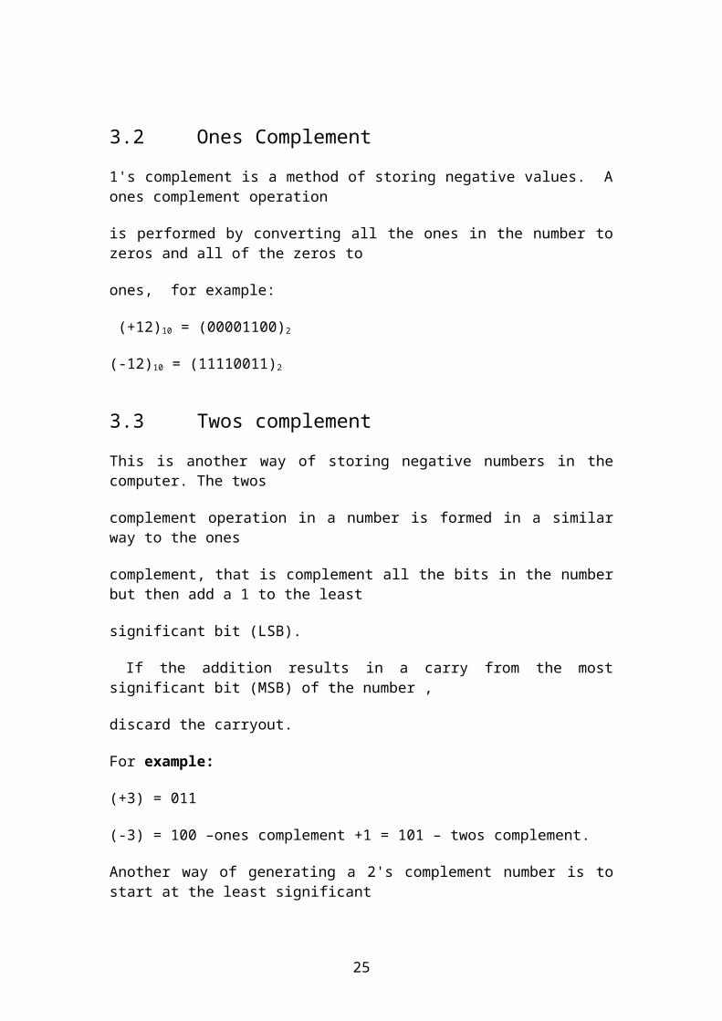
3.2 Ones Complement
1's complement is a method of storing negative values. A ones complement operation
is performed by converting all the ones in the number to zeros and all of the zeros to
ones, for example:
(+12)10 = (00001100)2
(-12)10 = (11110011)2
3.3 Twos complement
This is another way of storing negative numbers in the computer. The twos
complement operation in a number is formed in a similar way to the ones
complement, that is complement all the bits in the number but then add a 1 to the least
significant bit (LSB).
If the addition results in a carry from the most significant bit (MSB) of the number ,
discard the carryout.
For example:
(+3) = 011
(-3) = 100 –ones complement +1 = 101 – twos complement.
Another way of generating a 2's complement number is to start at the least significant
bit, and copy down all the 0's till the first 1 is reached. Copy down the first 1,and then
invert all the remaining bits
Example:
Dec No Binary value 1’s complement value 2’s complement value
7 0000111 11111000 11111001
32 0010000 11011111 11100000
19

Table of Complements
Binary 1’s complement 2’s complement Unsigned0111 7 7 70110 6 6 60101 5 5 50100 4 4 40011 3 3 30010 2 2 20001 1 1 10000 0 0 01111 -0 -1 151110 -1 -2 141101 -2 -3 131100 -3 -4 121011 -4 -5 111010 -5 -6 101001 -6 -7 91000 -7 -8 8
Observations to be made on this table are that in the case of 1’s complement there are
two representations of zero (0),and also note that when given positive and negative
numbers , the positive numbers do no change both in the 1’s and 2’s complements.
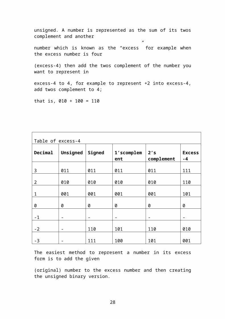
3.4 Excess Representation
Excess representation is also called biased representation. The numbers are treated as
unsigned. A number is represented as the sum of its twos complement and another
number which is known as the “excess” for example when the excess number is four
(excess-4) then add the twos complement of the number you want to represent in
excess-4 to 4, for example to represent +2 into excess-4, add twos complement to 4;
that is, 010 + 100 = 110
20

Table of excess-4
Decimal Unsigned Signed 1’scomplement 2’s complement Excess-4
3 011 011 011 011 111
2 010 010 010 010 110
1 001 001 001 001 101
0 0 0 0 0 0
-1 - - - - -
-2 - 110 101 110 010
-3 - 111 100 101 001
The easiest method to represent a number in its excess form is to add the given
(original) number to the excess number and then creating the unsigned binary version.
For example consider representing (+12) 10 and (-12) 10 in an eight-bit format using an
excess code 128 representation. Excess 128 number is formed by adding 128 to the
original number and then creating the unsigned binary version.
Example:
(+12) 10 = (128 + 12 = 140) 10
140 = (10001100) 2
For (-12) 10 = (128 – 12 = 116) 10
11610 = (01110100) 2
There is however no numerical significance of the excess value , only that it has the
effect of shifting the representation of the two’s complement numbers.
The excess value is chosen to have the same bit pattern as the largest negative
number. The advantage of excess representation is that it simplifies making
21

comparisons between numbers.
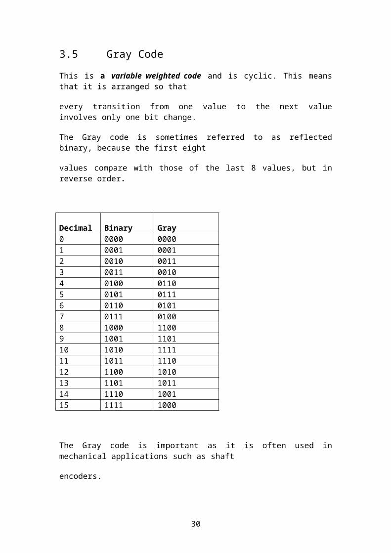
3.5 Gray Code
This is a variable weighted code and is cyclic. This means that it is arranged so that
every transition from one value to the next value involves only one bit change.
The Gray code is sometimes referred to as reflected binary, because the first eight
values compare with those of the last 8 values, but in reverse order.
Decimal Binary Gray0 0000 00001 0001 00012 0010 00113 0011 00104 0100 01105 0101 01116 0110 01017 0111 01008 1000 11009 1001 110110 1010 111111 1011 111012 1100 101013 1101 101114 1110 100115 1111 1000
The Gray code is important as it is often used in mechanical applications such as shaft
encoders.
22

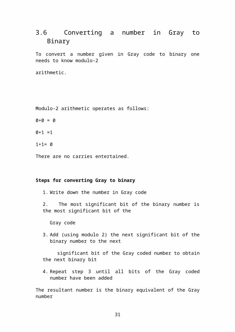
3.6 Converting a number in Gray to Binary
To convert a number given in Gray code to binary one needs to know modulo-2
arithmetic.
Modulo-2 arithmetic operates as follows:
0+0 = 0
0+1 =1
1+1= 0
There are no carries entertained.
Steps for converting Gray to binary
1. Write down the number in Gray code
2. The most significant bit of the binary number is the most significant bit of the
Gray code
3. Add (using modulo 2) the next significant bit of the binary number to the next
significant bit of the Gray coded number to obtain the next binary bit
4. Repeat step 3 until all bits of the Gray coded number have been added
The resultant number is the binary equivalent of the Gray number
Example:
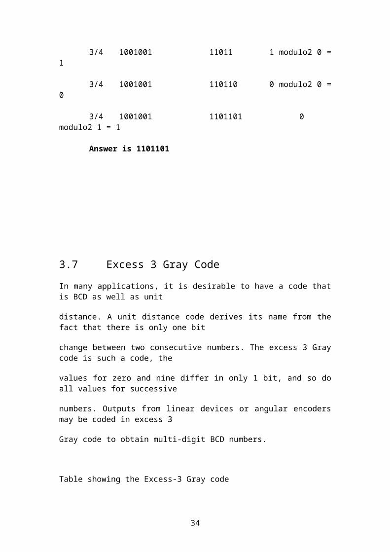
Convert 1101101 in Gray code to binary
Gray Binary1. 1101101
2. 1101101 1 copy down the MSB
3. 1101101 10 1 modulo2 1 = 0
23

4. 1101101 100 0 modulo2 0 = 0
3/4 1101101 1001 0 modulo2 1 = 1
3/4 1101101 10010 1 modulo2 1 = 0
3/4 1101101 100100 0 modulo2 0 = 0
3/4 1101101 1001001 0 modulo2 1 = 1
Answer is 1001001
24
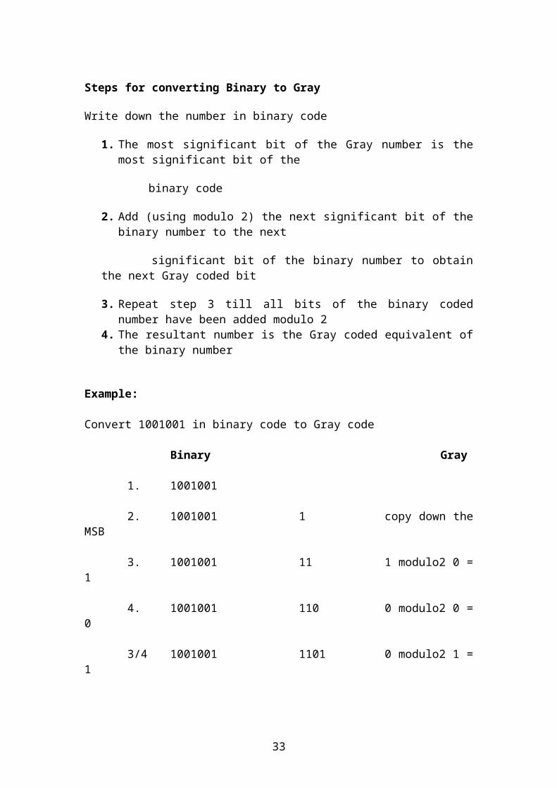
Steps for converting Binary to Gray
Write down the number in binary code
1. The most significant bit of the Gray number is the most significant bit of the
binary code
2. Add (using modulo 2) the next significant bit of the binary number to the next
significant bit of the binary number to obtain the next Gray coded bit
3. Repeat step 3 till all bits of the binary coded number have been added modulo 2
4. The resultant number is the Gray coded equivalent of the binary number
Example:
Convert 1001001 in binary code to Gray code
Binary Gray
1. 1001001
2. 1001001 1 copy down the MSB
3. 1001001 11 1 modulo2 0 = 1
4. 1001001 110 0 modulo2 0 = 0
3/4 1001001 1101 0 modulo2 1 = 1
3/4 1001001 11011 1 modulo2 0 = 1
3/4 1001001 110110 0 modulo2 0 = 0
3/4 1001001 1101101 0 modulo2 1 = 1
Answer is 1101101
25

3.7 Excess 3 Gray Code
In many applications, it is desirable to have a code that is BCD as well as unit
distance. A unit distance code derives its name from the fact that there is only one bit
change between two consecutive numbers. The excess 3 Gray code is such a code, the
values for zero and nine differ in only 1 bit, and so do all values for successive
numbers. Outputs from linear devices or angular encoders may be coded in excess 3
Gray code to obtain multi-digit BCD numbers.
Table showing the Excess-3 Gray code
Decimal Excess-3 Gray Code
0 00101 01102 01113 01014 01005 11006 11017 11118 11109 1010
3.8 Range and Precision in Floating Point Numbers
One of the advantages of floating point representation is that this format allows a
large range of expressible numbers to be represented in a smaller number of digits by
26

separating the digits used for precision from those digits used for range.
Example of base 10 floating-point number: +6.023 x 10²³
The range is represented by power f ten that is, 1023.
The digits in the fixed-point number 6.023 represent precision
+ (Sign), 23 (exponent), 6.023 (Significant)
The potential problem with representing floating numbers is that the same number can
be represented in different ways which makes comparisons and arithmetic operations
difficult, for example 3584.101 = 3.584 x 103 = .3584 x 104.
To avoid these multiple representations of the same number, the number must be
normalised by shifting the radix point to the left or to the right and the exponent must
be adjusted accordingly, until the radix point is to the left of the leftmost non-zero
digit. So the number .3584 x 104 is a normalised one.
3.9 Representing floating point numbers in the computer.
A simple floating-point format to illustrate the important factors in representing
floating point numbers in the computer may have the form shown below:
sign bit, three bit exponent , .implied radix point , three base 16 digits
The significant is signed; the three hexadecimal digits are for the magnitude.
The exponent is a 3-bit excess 4 number with radix of 16. The bits will be packed as
follows:
Sign bit on the left, followed by a three bit exponent, followed by three hexadecimal
digits of the significant.
Example:
Convert (358) 10 to the format given above.
27
Step 1: Convert the fixed point number from its original base into a fixed point
number in the target base.. We will use the remainder theorem.
Original base Integer Remainder
358/16 22 6 LSB
22/16 1 6
1/16 0 1 MSB
So (358) 10 = (166) 16
Step 2: Convert the fixed-point number to floating point number
(166) 16 = (166.) 16 x 160
Step 3: Normalise the number, for example
(166.) 16 x 160 = (.166) 16 x 163
Step 4: write the bit fields of the number. The number is positive so in the sign bit
position write a zero(0). The exponent is 3 but should be represented as excess-4, so
the bit pattern for the exponent is calculated as follows;
011(+3)10
Exceaa-4 = 011+100 = 111
Step 5: Each of the base 16 digits is represented in binary as 1=0001, 6= 0110 and
another 6 = 0110.
0 111 0001 0110 0110
+(sign) (exponent) (1) (6) (6)
The bit pattern is stored in the computer’s memory as 0111000101100110
Example:
Convert (9.375 x10⁻²) to base 2 scientific notation
Step 1: Convert from base 10 floating point to base 10 fixed point by moving the
28

decimal point two places to the left.
Step 2: Convert from base 10 fixed point to base 2 fixed point using the
multiplication method.
Step 3: Convert to normalised base 2 floating point
We follow all the steps to solve the problem
9.375 x 10-2 = .09375
.09375 x 2 = 0.1875
.1875 x 2 = 0.375
.375 x 2 = 0.75
75 x 2 = 1.5
5 x 2 = 1.0
(.09375) 10 = (.00011) 2
.00011 = .00011x 20
= 1.1 x 2-4
(.00011)
.
29
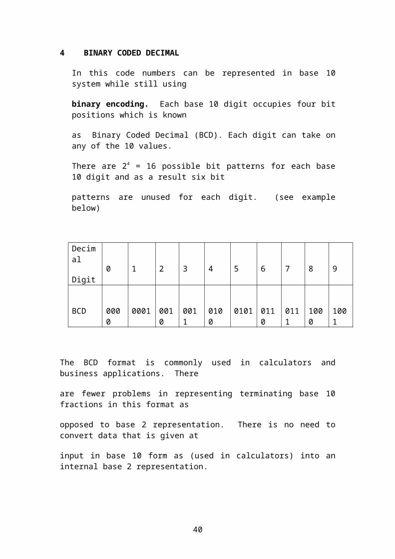
4 BINARY CODED DECIMAL
In this code numbers can be represented in base 10 system while still using
binary encoding. Each base 10 digit occupies four bit positions which is known
as Binary Coded Decimal (BCD). Each digit can take on any of the 10 values.
There are 24 = 16 possible bit patterns for each base 10 digit and as a result six bit
patterns are unused for each digit. (see example below)
Decimal
Digit 0 1 2 3 4 5 6 7 8 9
BCD 0000 0001 0010 0011 0100 0101 0110 0111 1000 1001
The BCD format is commonly used in calculators and business applications. There
are fewer problems in representing terminating base 10 fractions in this format as
opposed to base 2 representation. There is no need to convert data that is given at
input in base 10 form as (used in calculators) into an internal base 2 representation.
4.1 Representing signed numbers in BCD
Signed BCD numbers are represented in the computer using:
(i) Nines and Tens complement
(ii) Nines’ complement
(iii)Tens complement
30
4.2 NINES AND TENS COMPLEMENT
In the nines complement number system, positive numbers are represented as ordinary
BCD numbers but the leftmost digit(sign digit) is less than five (5) for positive
numbers and five or greater for negative numbers.
Example:
(+301) 10 0000 0011 0000 0001
(0)10 (3)10 (0) (1)
(Nines and Tens complement)
4.2.1 Nines complement (Negative)
Subtracting each digit from nine forms the nines complement negative, for example
9 – 0 = 9; 9 – 3 = 6; 9 – 0 = 9; 9 – 1 = 8.
(-301) 10 1001 0110 1001 1000
(9) 10 (6) 10 (9) 10 (8)10
Nines complement (negative)
4.2.2 Tens complement (Negative)
The tens complement negative is formed by adding a 1(one) to the nines complement
negative.
For example:
(-301) 10 = 9698 + 1 = 9699
= 1001 0110 1001 1001
(9) 10 (6) 10 (9) 10 (9) 10
31

5 COMPUTER CODES
Character Codes – these are: ASCII, EBCDIC, UNICODE.
5.1 ASCII (American Standard Code for Information Interchange)
-Is a standard seven-bit code that was proposed 1963, and finalized in 1968. ASCII
was established to achieve compatibility between various types of data processing
equipment. ASCII, pronounced "ask-key", is the common code for microcomputer
equipment. The standard ASCII character set consists of 128 decimal numbers
ranging from zero through 127 assigned to letters, numbers, punctuation marks, and
the most common special characters. ASCII Character Set also consists of 128
decimal numbers and ranges from 128 through 255 representing additional special,
mathematical, graphic, and foreign characters. 7 bits represent each character and an
eighth bit is used for parity. The parity bit is used to detect the presence of errors
during data entry or transmission
Some of the special characters include:
00 NUL Null
01 SOH Start of Heading
02 STX Start of text
03 ETX End of text
04 EOT End of transmission
05 ENQ Enquiry
06 ACK Positive Acknowledgement
07 NAK Negative Acknowledgement
32
Example of ASCII character set
0 1 2 3 4 5 6 7 8 9 A B C D E F
0 NUL SOH STX ETX EOT ENQ ACK BEL BS HT LF VT FF CR SO SI
1 DLE DC1 DC2 DC3 DC4 NAK SYN ETB CAN EM SUB ESC FS GS RS
2 SP ! " # $ % & ' ( ) * + , - . /3 0 1 2 3 4 5 6 7 8 9 : ; < = > ?4 @ A B C D E F G H I J K L M N O5 P Q R S T U V W X Y Z [ \ ] ^ _6 ` a b c d e f g h i j k l m n o7 p q r s t u v w x y z { | } ~ DEL
All characters in ASCII use Hexadecimal indices, which makes character
manipulation simpler.
5.2 EBCDIC – (Extended Binary Coded Decimal Information Code)
-Is an eight-bit character set that was developed by International Business Machines
(IBM). It was the character set used on most computers manufactured by IBM prior to
1981. EBCDIC is not used on the IBM PC and all subsequent "PC clones". These
computer systems use ASCII as the primary character and symbol coding system.
EBCDIC is widely considered to be an obsolete coding system, but is still used in
some equipment, mainly in order to allow for continued use of software written many
years ago that expects an EBCDIC communication environment.
33
Example of EBCDIC special characters
SOH Start of Heading
STX Start of Text
EXT End of Text
PF Punch Off
HT Horizontal Tab
LC Lower Case
DEL Delete
SMM Start of Manual Message
VT Vertical Tab
FF Form Feed
CR Carriage Return
SO Shift Out
SI Shift In
DLE Data Link Escape
Most of the characters in this set are the same as those used in ASCII except
for some special symbols as shown above.
5.3 UNICODE
The UNICODE was developed to support characters that are outside the historical
dominant (Latin) character sets used in computers. Remember ASCII and EBCDIC
codes support the Latin character sets. The UNICODE is a universal character
standard that supports the a greater number of the world’s character set. The
current version (4.0) of the UNICODE standard version developed by the
34

UNICODE Consortium assigns a unique identifier to each of 96,382 characters
(increased from 95,156 in version 3.2), covering the scripts of the world’s principal
written languages and many mathematical and other symbols. A previous version
(2.1) of the Unicode Standard encompassed 38,887 characters and was adopted as part
of the recommendations for HTML 4.0.
Example of Unicode Characters
! 5 A a ¥ ¼ Ñ ñ Ą ą IJ ij Ə Ύ δ Δ Љ Щ щ fi بא ב ۳؟ ♪♀
☺ Ẁ Ặ ỳ ₣ ₪ € № ™
The above UNICODE characters cover principal written languages of the Americas,
Europe, the Middle East, Africa, India, Asia and the Pacifica. The UNICODE
STANDARD is a character coding system designed to support the worldwide
interchange, processing, and display of the written texts of the diverse languages and
technical disciplines of the modern world. In addition, it supports classical and
historical texts of many written languages.
35

6 BOOLEAN ALGEBRA
Boolean algebra is the most fundamental tool necessary to analyse and describe the
logic of digital circuits. A Boolean variable A can take only two valuations, a 1 or 0,
which have also the logic interpretations True for a 1 and False for a 0 or High for a 1
and Low for a 0, and On for a 1 and Off for a 0. The operations of a Boolean variable
are ., + and - , which are interpreted as AND(.), OR(+) and NOT(-). Boolean
equations are formed from Boolean variables which are linked by Boolean operators
for example:
. The application A.B can be written simply as AB.
6.1 PROPERTIES OF BOOLEAN ALGEBRA
The basic properties of Boolean algebra are:
Commutative
Distributive
Identity
Complement
These properties are applied to logic expressions (equations) and they are also known
as postulates. These postulates are basic axioms of Boolean algebra and need no
proofs.
36

Examples:
Relationship Dual Property
AB = BA A+B = B+A Commutative
A(B+C) = AB+AC A+BC =(A+B)(A+C) Distributive
1.A = A 0+A=A Identity
Complement
All Boolean algebra theorems can be proved using postulates. The dual form is
obtained by changing ANDs to ORs and vice-versa.
The commutative property sates that: The order that two Boolean variables appear
in an AND or OR function is not significant, that is (AB=BA), (A+B) = (B+A).
The distributive property shows how a variable is distributed over an expression with
which it is ANDEd for example A(B+C) = AB+AC or A+BC= (A+B)(A+C).
The identity property staes that a variable that is ANDEd with a 1 or is ORed with a
0 produces the original variable that is 1.A = A or 0 + A = A.
The complement is derived from the involution theorem whish states that the
complement of a complement leaves the original variable unchanged.
6.2 DE MORGAN’S THEOREM
This theorem has the most significance in that it is a technique for substuting AND
operators for OR operators and vice-versa. For example the logic function A+B when
subjected to De Morgan theorem forms the equality:
and also that:
37

Summary of Relationships in Boolean algebra
T1 (a) A+B = B+A
(b) A.B = B.A
T2 (a) (A+B)+C = A+(B+C)
(b) (A.B). C = A. (B.C)
T3 (a) A. (B+C) = A.B+A.C
(b) (A+B). (A+C) = A+B.C
T4 (a) A+A=A
(b) A.A = A
T5 (a)
(b)
T6 (a) A+A.B = A
(b) A. (A+B) =A
T7 (a) 0+A = A
(b) 1+A =1
(c) 1.A = A
(d) 0.A = 0
T8 (a)
(b)
T9 (a)
(b)
38

7 LOGIC GATES
A logic gate is a physical device that implements a simple Boolean function. The
Logic gates form the hardware basis on which digital computers are built. Logic gates
are also called logic circuits. The elementary (basic) logic gates are:
NOT, BUFFER, OR, AND, NOR, NAND, EXCLUSIVE OR (XOR) and
Exclusive NOR (XNOR).
7.1 NOT Logic gate
- is also called an INVERTER and it produces a 1 at its output for a
zero (0) input that is, the output is always the opposite or complement of the input.
Symbol
Truth Table
X Y
0 1
1 0
BUFFER
A buffer simply copies its input to its output. A buffer has no logical significance, but
it serves an important practical role as an amplifier, that is it allows a number of
logical gates to be driven by a single signal.
39
Symbol
X F
Truth table
X F
0 0
1 1
7.2 The OR Logic Gate
The basic OR gate works with two inputs and 1 output. The output of the OR gate is
true (logical 1) when either one or both inputs are logical ones (1s) and is false
otherwise (0)
Symbol
Truth Table
X Y F0 0 0
0 1 1
1 0 1
1 1 1
Note that the output value is 1 when at least one input value is 1
40

7.3 The AND logic gate
A basic AND logic gate operates with two inputs and one output. The output of an
AND gate is a logical 1, only and only when both of its inputs are logical 1s and is
false otherwise
Symbol
Truth Table
X Y F
0 0 0
0 1 0
1 0 0
1 1 1
Note that the output is 1 only when both inputs are 1
7.4 The NOR logic gate
The NOR gate is formed by connecting an INVERTER (NOT gate) at the output of an
OR gate. This gate produces complementary outputs to the OR gate.
41

Symbol
Truth Table
X Y F
0 0 1
0 1 0
1 0 0
1 1 0
7.5 The NAND logic gate
The NAND logic gate is formed by connecting a NOT gate at the output of an AND
gate and this gate produces complementary outputs to the AND gate.
Symbol
Truth Table
X Y F
0 0 1
0 1 1
1 0 1
1 1 0
42

7.6 The EXclusive OR (XOR) logic gate
Exclusive OR (XOR) logic gate produces a logical 1 at its output when either
one of its input is a 1, excluding cases when both inputs are logical 1s and logical
0s(zeros).
Symbol
Truth Table
X Y F
0 0 0
0 1 1
1 0 1
1 1 0
Note that when both inputs are 1s the output is a 0.
7.7 EXclusive NOR (XNOR) logic gate
This logic gate is formed by connecting an INVERTER to the Exclusive OR gate and
it produces outputs that are complementary to those of the Exclusive OR gate.
43

Symbol
Truth Table
X Y F
0 0 1
0 1 0
1 0 0
1 1 1
44

8 KARNAUGH MAPS
Karnaugh maps are a very effective way of minimizing/reducing/simplifying Boolean
functions/expressions/equations.
The Karnaugh maps are a variation of the truth tables. Because all Boolean functions/
logic functions convert to logic circuits in a computer, any reduction of the functions
will result in the following:
Hardware cost savings
Reduced propagation delays
Simplification of the circuits
High productivity
The basic concept behind Karnaugh maps is to reduce a function such as:
, by utilising the relationship/postulate .
The Karnaugh map works best with two, three, four, five and six variables, but
becomes clumsy, complex and almost impossible to use with seven or more variables.
8.1 One variable Karnaugh map
A one variable Karnaugh map has two possible states, for example if a variable is
designated by symbol A, then A can take the logical symbol 1 (A = 1) or value 0
. The single variable map contains two equal divisions known as cells. One
half represents state A and the other half state
8.2 Two variable Karnaugh map
The two variable map has four possible states and each variable is represented by half
the total number of cells (see example below). The cells are represented by
45

numbers, which can be used to quicken the process of minimization , for
example 00 is (0), 01 is 1, 10 is 2 and 11 is 3.
A 0 1 B
(00) (10)
AB (01) (11)
8.3 The three variable Karnaugh map
The three variable Karnaugh map has 23 possible combinations of the input variables
and each variable occupies exactly half the total number of cells.
Example:
AB 00 01 11 10C 0 (000) (010) (110) (100)
ABC 1 (001) (011) (111) (101)
The cells are represented by numbers, for example (000) is 0, (001) is , (010) is 2,
(011) is 3, (100) is 4, (101) is 5, (110) is 6 and (111) is 7. This numbering quicken the
process of inserting the ones(1s) in cells during minimisation of Boolean functions.
46

8.4 The Four variable Karnaugh map
The four variable Karnaugh map has 24 possible input combinations and each variable
occupies exactly half the total number of cells in the whole map.
Example:
AB 00 01 11 10CD 00 0000 0100 1100 1000 (0) (4) (12) (8) (1) (5) (13) (9) 01 0001 0101 1101 1001 11 0011 0111 1111 1011 (3) (7) (15) (11) (2) (6) (14) (10) 10 0010 0110 1110 1010
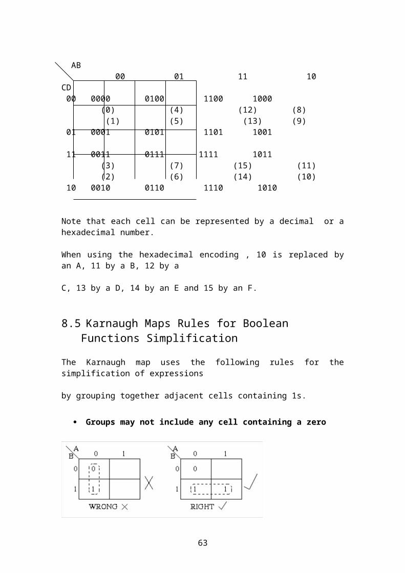
Note that each cell can be represented by a decimal or a hexadecimal number.
When using the hexadecimal encoding , 10 is replaced by an A, 11 by a B, 12 by a
C, 13 by a D, 14 by an E and 15 by an F.
8.5 Karnaugh Maps Rules for Boolean Functions Simplification
The Karnaugh map uses the following rules for the simplification of expressions
by grouping together adjacent cells containing 1s.
Groups may not include any cell containing a zero
So the function on the right reduces to: F = B
47

Groups may be horizontal or vertical, but not diagonal.
The above function reduces to: F = A+B
Groups must contain 1, 2, 4, 8, or in general 2n cells.
That is if n = 1, a group will contain two 1's since 21 = 2.
If n = 2, a group will contain four 1's since 22 = 4.
48

Each group should be as large as possible.
Although no Boolean rules have been broken on the right three variable map, it
can still be reduced to , the equivalent of the correct groupings.
Each cell containing a one (1) must be in at least one group.
49

Groups may overlap.
Groups may wrap around the table. The leftmost cell in a row may be
grouped with the rightmost cell and the top cell in a column may be grouped
with the bottom cell.
There should be as few groups as possible, as long as this does not
contradict any of the previous rules.
50

The function on the left above reduces to :
. Note that the map on the right (wrong) is wrong because the groupings
do not produce the minimal result as it can still be reduced to :
EXAMPLES OF MINIMISING FOUR VARIABLE MAPS
DC BA 00 01 11 10
00 1 0 0 1
01 0 0
11 1 1 0 0
10 1 1 0 0
DC BA 00 01 11 10
00 1 1 0 1
01 0 0 1
11 1 1 0 0
10 1 0 0 0
51
1 1
1 1 1 1 1
1
11
1
1 1
1
1
1 1
1 1
1 1

DC BA 00 01 11 10
00 1 11 0 1
01 0 1
11 1 1 0 0
10 0 1 0 0
DC BA 00 01 11 10
00 1 0 0 1
01 0 0 0
11 1 0 0 0
10 1 1 0 0
8.6 WORKING WITH DON’T CARE CONDITIONS
There are two cases when don’t care conditions can arise.
The first case is when the designer does not care what the output will provide. This
can be illustrated by an example of the S, R flip-flop truth table below.
S R Q
0 0 0 1
0 1 0 1
The two conditions R = 0, R=1 are collectively called a don’t care condition because
52
1 1
1 1
1
1
1
1
1
11 1 1
1
1

in each case the result at the outputs are the same. So this means that it does not
matter whether R=1 or R= 0, as long as S = 0 the outputs at the Q and remain the
same, so the designer has the liberty to use what is at his/her disposal or what is less
expensive.
The other simple example is when designing say a machine to report the voting
outcome when 4 people vote. Two binary outputs are used. If one output is assigned
to a indicate a tie then we don’t care what the YES/NO output shows when there is a
tie.
The second case is when the inputs will never occur as is the case with a binary coded
decimal to seven-segment decoder, where we only use the inputs from 0 to 9 and the
other six states remain unused.
When using don’t care conditions in Karnaugh maps the minimum requirement is that
the number of don’t care conditions in a group must be equal to the number of 1s.
However a group may contains more ones than don’t care conditions.
Examples of using don’t care conditions with four variable Karnaugh maps
In all the examples the xs indicate don’t care conditions and all the rules for
simplification of Boolean functions apply.
53

DC BA 00 01 11 10
00 1 0 x 1
01 0
11 1 1 x x
10 1 1 x x
DC BA 00 01 11 10
00 1 1 x 1
01 1 0 x 1
11 1 1 x x
10 1 0 x x
DC BA 00 01 11 10
00 1 1 x 1
01 1
11 1 1 x x
10 0 1 x x
DC
54
x 1 1
1 x
1 1 x x
1 x
1 x
1 1 x x
1 1 x 1
1 1 x 1
1 1 x 1 11 1 x 1
1 1 x x
1
1 x
1 x
1 x
1 x
x 1
x 1
1 1 x x x
1 1 x 1
1 1 x 1 11 1 x 1
1 1 x x
1
1 x
1 x
1 x
1 x

BA 00 01 11 10
00 1 0 x 1
01 0 0
11 1 0 x x
10 1 1 x xx
55

9 COMBINATIONAL AND SEQUENTIAL CIRCUITS
(Implementation of logic gates)
A combinational circuit is a logic circuit, whose output entirely depends on the inputs,
that is the output is always a function of the inputs. The circuit has no storage
capabilities (see block diagram below)
Combinational circuits can be used to build devices for solving problems of simple
logic nature
The array of outputs Yo – Yn entirely depend on the array of inputs Xo- Xn.
Combinational circuits can be used to build devices for solving problems of simple
logic nature.
The typical examples of combinational logic circuits are logic gates, half adders, full
adders, multiplexers, decoders, etc.
9.1 ADDERS
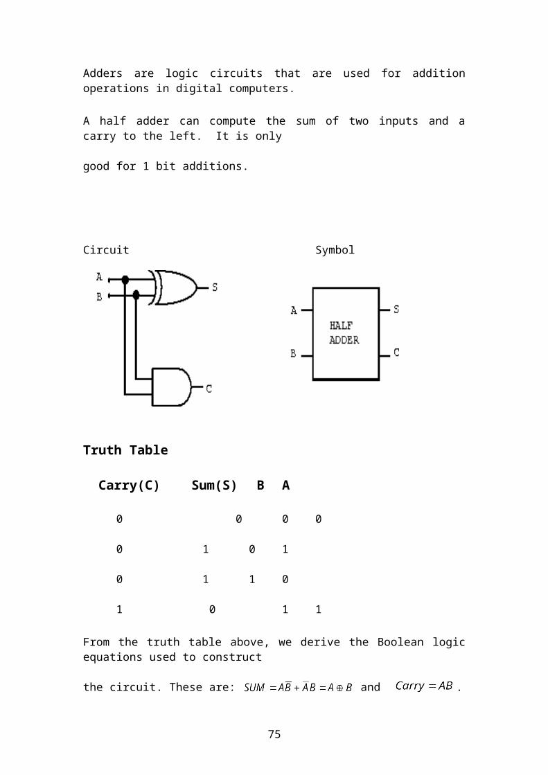
Adders are logic circuits that are used for addition operations in digital computers.
A half adder can compute the sum of two inputs and a carry to the left. It is only
good for 1 bit additions.
56

Circuit Symbol
Truth Table
Carry(C) Sum(S) B A
0 0 0 0
0 1 0 1
0 1 1 0
1 0 1 1
From the truth table above, we derive the Boolean logic equations used to construct
the circuit. These are: and .
57

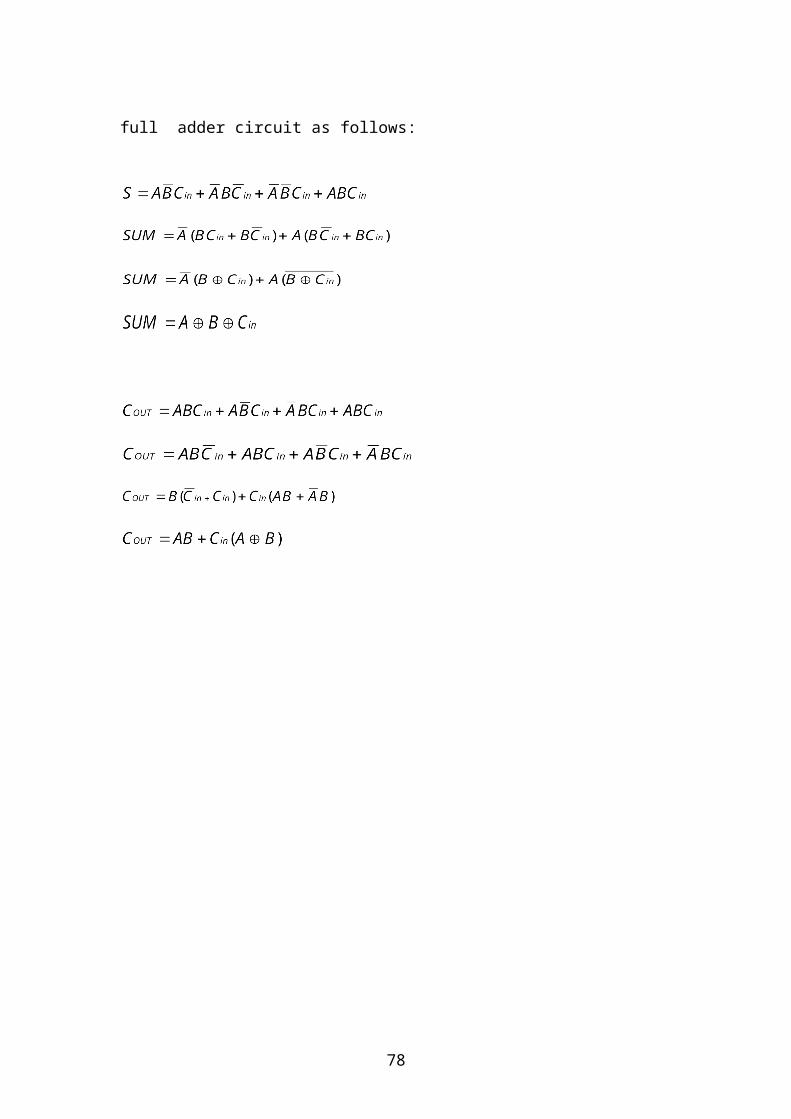
9.2 FULL ADDER
Full adder was developed to overcome the limitations of the half adder, that is , its
in ability to handle a carry into position from the right. The full adder is built on
two half adders(circuit diagram below)
Truth Table
9.2.1.1 Carry Out(C) Sum( S) Carry in(Cin) B A
0 0 0 0 0
0 1 0 0 1
0 1 0 1 0
1 0 0 1 1
0 1 1 0 0
1 0 1 0 1
1 0 1 1 0
1 1 1 1 1
58

From the truth table, we derive the logic equations for building the
full adder circuit as follows:
9.3 REDUCTION OF COMBINATIONAL CIRCUITS
59

In many cases the sum of products or product of sums forms of Boolean equations is
not the minimal in terms of their number and size. Smaller Boolean equations
translate to a lower gate input counts in the target circuits. So the reduction of an
equation is an important consideration when circuit complexity is an issue.
We have already looked at the Karnaugh map method of minimising Boolean
equation and the benefits derived from its use. We will look at the algebraic method
by way of an example.
Consider the Boolean equation:
. The properties of Boolean algebra can be used to
reduce the equation.
Distributive property (1)
Complement property (2)
Identity property (3)
We can reduce equation 3 by introducing the property Idempotence and re-
introducing ABC, for example:
Idempotence (4)
Distributive (5)
Identity (6)
We can also re-introduce ABC to equation 6, for example
Idempotence (7)
Distributive (8)
Identity (9)
From the above equation, it is clear to see that the, the original equation is not minimal and has four AND gates, three OR gates and three NOT gates. The total
number of gates is ten (10).
60

Equation 9, which is the minimal form of the original equation, has three AND gates
and one OR gate. The total number of gates is five( 5). This means that the
total number of logic gates has been reduced by five(half). This simplifies the circuit,
save components costs and also reduces propagation delays.
Example 1:
Express the Boolean equation below in its minimal form
Example 2:
Show that:
B can be written as
Complement property
This is by absorption
Since the second expression in parenthesis is the same as the first expression it
follows that:
= A + C
(A+B)(A+C) = A + BC9.4 DECODER
A decoder is a logic circuit that translates a logical encoding into a spatial
location. At any given time exactly one output of a decoder is high(logical 1) and is
61

determined by the settings on the control inputs.
A decoder is used to control other circuits and at times it may be inappropriate to
enable any of the other circuits. For that reason an enable line is added to the
decoder, which forces all outputs to 0 if a zero is applied to its input. IN is the enable
line. When IN = 1, the circuit is active and when N=0, the whole circuit is inhibited.
The other important application of a decoder is to translate memory addresses into
physical locations.
A 3 to 8 decoder
62
This circuit will selects one output at any given time and this depends on the input
combinations.
Outputs D0 to D7 can be specified by Boolean equations, for example,
9.5 MULTIPLEXER (MUX)
A multiplexer is a component/device/logic circuit that a connects a number of inputs
to a single output.(see circuit diagram below)
63

The output F takes on the value of the data input that is selected by control lines S1
and S2. If S1S2 = 00, the value on line D0 ( either a one(1)or a zero(0) will appear
at F and the output at F at any given time is given by the Boolean logic equation:
9.6 DE MULTIPLEXER (DEMUX)
A DEMUX is the converse of a MUX. It has one data input and any outputs. Data
can be transferred from this single input to one of its many outputs. The application of
64

DEMUX is to send data from a single source to one of a number of destinations.
The circuit above can still be used as a De Multiplexer/Decoder.
IN is used as the single data input and will send data to one of the many outputs,
that is, OUT0 TO OUT3.
10 SEQUENTIAL CIRCUITS
These are also called sequential logic units and are commonly referred to as finite
state machines (FSM). The output of a sequential circuit depends on present inputs,
65

present states and also the previous states. The basic sequential circuit is a flip flop.
10.1Flip Flop Circuits
These are the basic components of memory systems. The basic flip flop is called a
Latch, that is a logic gate that can somehow “remember” the previous input values.
A basic one bit memory can be created using two NOR gates or two NAND gates.
Example of a 1 bit memory built on NOR gates is shown below.
The diagram above is known as an SR latch.
It has two inputs:
(i) S for setting the latch on(ii) R for resetting the latch(clearing it to zero (0)
Has also two outputs Q and which are complementary.
The Latch operates as follows:
When R = 0 and S = 0, the signal from R enters the NOT gate and is complemented into a one (1) and the one is stored at output and is also fed back to the lower gate
The operation of a latch is best described by its truth table.
R S Q
0 1 1 0 set latch to 1
66

1 0 0 1 reset latch(clear to zero)
0 0 0 1 no change
1 1 x x prohibited (ambiguous state)
A basic one bit memory can be created using two NAND gates
The circuit shown above is a basic NAND latch. The inputs are generally
designated "S" and "R" for "Set" and "Reset" respectively.
Because the NAND inputs must normally be logic 1 to avoid affecting the
latching action, the inputs are considered to be inverted in this circuit.
The outputs of any single-bit latch or memory are traditionally designated Q
and . In a commercial latch circuit, either or both of these may be available
for use by other circuits.
For the NAND latch circuit, both inputs should normally be at a logic 1 level.
Changing an input to a logic 0 level will force that output to a logic 1.
The same logic 1 will also be applied to the second input of the other NAND
gate, allowing that output to fall to a logic 0 level. This in turn feeds back to the
second input of the original gate, forcing its output to remain at logic 1.
Applying another logic 0 input to the same gate will have no further effect on this
67

circuit. However, applying a logic 0 to the other gate will cause the same reaction in
the other direction, thus changing the state of the latch circuit the other way.
Note that it is forbidden to have both inputs at a logic 0 level at the same time.
That state will force both outputs to a logic 1, overriding the feedback latching
action. In this condition, whichever input goes to logic 1 first will lose control,
while the other input (still at logic 0) controls the resulting state of the latch. If
both inputs go to logic 1 simultaneously, the result is a "race" condition, and
the final state of the latch cannot be determined ahead of time.
Truth Table
Q
0 0 0 1 no change
1 0 1 0 set to 1
0 1 0 1 reset to zero (clear to 0)
1 1 x x prohibited
The combination S = R ; Q = is not allowed because it produces an
indeterminate next state and is also called an ambiguous state because it
produces a” race” condition, the next state of which cannot be determined
ahead of time. The ambiguous state makes the S R latch difficult to manage
and for this reason, it is seldomly used in practice.10.2Clocked R S Flip Flop
A clock is a circuit that emits a series of pulses with precise pulse width and a
precise interval between consecutive pulses called, a clock cycle time.
Pulse frequency commonly used in practice are between 1 and 100MHZ and
68

this corresponds to 1000 and 10 nsec. A clock is used in a latch to prevent it
from changing states except at certain specific times.
Clocked RS Truth Table
R S Q
0 1 1 0 set latch to 1
1 0 0 1 reset latch(clear to zero)
0 0 0 1 no change
1 1 x x prohibited (ambiguous state
This flip-flop circuit is improved by adding timing input. In that case the output will
change only when the input clock is high. This flip-flop circuit is improved by
adding timing input. In that case the output will change only when the input clock is
high.
10.3JK Flip-flop (Universal Flip-flop)
In this case the prohibited state of RS flip-flop is removed.
69

The J, K flip flop is a modification of the RS flip flop developed to remove the
ambiguous case when S = R = 1 ; Q = = 0. The outputs of the JK flip flop are fed
back into the AND gates. The letters J and K are universally used to distinguish the
JK flip flop from the SR flip flop, but they do not stand for anything in particular.
The problem with the JK flip flop is that when J =1, K=1 and the clock C =1, the flip
flop may toggle more than once.
This problem can be eliminated by the use of the JK Master Slave flip-flop
Clocked JK Truth Table
C J K Q
1 1 0 1 0 set latch to 1
1 0 0 0 1 reset latch (clear to zero)
1 0 0 0 1 no change
1 1 1 1 0 toggle previous state
70

10.4 JK Master Slave flip-flop built on NAND gates
If both the J and K inputs are held at logic 1 and the CLK signal continues
to change, the Q and Q' outputs will simply change state with each falling edge
of the CLK signal. (The master latch circuit will change state with each rising
edge of CLK.) We can use this characteristic to advantage in a number of ways.
A flip-flop built specifically to operate this way is typically designated as a T
(for Toggle) flip-flop. The lone T input is in fact the CLK input for other
types of flip-flops. The JK flip-flop must be edge triggered in this manner. Any
level-triggered JK latch circuit will oscillate rapidly if all three inputs are held
at logic 1. This is not very useful. For the same reason, the T flip-flop must also
be edge triggered. For both types, this is the only way to ensure that the flip-
flop will change state only once on any given clock pulse. Because the
behaviour of the JK flip-flop is completely predictable under all conditions, this
is the preferred type of flip-flop for most logic circuit designs. The RS flip-flop
is only used in applications where it can be guaranteed that both R and S
cannot be logic 1 at the same time. The JK master slave flip flop eliminates the
problem of toggling more than once but has a problem of being expensive as it
71

is built on two JK flip flops.
JK Master Slave Flip Flop Truth Table
C J K Q’ Q
1 1 0 1 0 1 0
1 0 1 0 1 0 1
10.5D flip-flop (Delay Flip-flop)
The D Flip Flop is the best way to avoid the R S flip flop ambiguity. This is
achieved by using a flip flop with only one input D. The input of the upper gate is
always the complement of the lower gate, so the problem of both inputs being logical
1s(ones) does not arise.
The D flip flop functions as follows:
When D is equal to 1 and the clock is equal to one, the flip flop is driven into logical
State 1. When D =0 and the clock equals to a 1, the current value of D is sampled and
stored in the flip flop.
72

D Flip Flop Truth Table
C D Q
1 0 0 1
1 1 1 0
D Flip Flop State diagram
D =1
D = 0 D = 1
D = 0
10.6EDGE TRIGGERED FLIP FLOPS
The JK flip flop eliminates the SR ambiguity but has a problem of toggling more than
once. The JK master slave flip flop eliminates the problem of toggling more than
once but has the disadvantage of being expensive since it is built on two JK flip flops.
The edge triggered flip flops are the most common type of flip flops in use. In this
type of flip flop transitions occur at specific level of the clock pulse. When the pulse
input level exceeds this threshold level, the inputs are locked out so that the flip flop
is unresponsive to further changes in inputs until the clock pulse returns to zero(0) and
other pulse occurs.
Edge triggered flip flops cause transitions on the rising edge of the clock
pulse(positive edge transition) or on the falling edge of the clock(negative edge
transition).
73
0 1

clk t
output cannot change
The value in the input cannot change when the clock is in the 1 level, in the 0 level or
in the 1 to 0 transition.
10.7EXCITATION TABLES
Excitation Tables are derived from the characteristic tables of flip flops. The truth
tables specify the next state when the inputs and present states are known.
During designing, the designer usually knows the required transition from present
state to next state but wishes to find out the flip flop input conditions that will cause
the required transition. So an excitation table lists the required input combinations for
a given change of state. The excitation tables can be produced from flip-flop truth
tables or from state diagrams.
Excitation Table of the SR flip flop
Q (t) Q (t+1) S R
0 0 0 x
0 1 1 0
1 0 0 1
1 1 x 0
The SR excitation table shows that there are four possible transitions from present
74
State Q (t) to next state Q (t+1). The symbol x in the table represents a don’t care
condition, that is it does not matter whether the input to the flip flop is a 1 or 0, the
result will be the same.
Excitation Table for the JK flip flop
Q (t) Q (t+1) J K
0 0 0 x
0 1 1 x
1 0 x 1
1 1 x 0
The reason for the don’t care conditions in the table means that there are two ways of
achieving the required transition, for example in the JK flip flop transition from state
0 to next state 0 can be achieved by having input J and K = 0(to obtain no change) or
by letting J = 0 and K = 1 to clear the flip flop(although it is already cleared).
The D Flip Flop Excitation Table
Q (t) Q (t+1) D
0 0 0
0 1 1
1 0 0
1 1 1
75

10.8SEQUENTIAL CIRCUIT EQUATIONS
Example of a sequential circuit diagram
The diagram next page shows a typical example of a sequential circuit.
The AND gates, OR gates and the INVERTER (NOT gate) form the combinational
logic part of the circuit.
The two D flip-flops form the storage part of the sequential circuit.
The interconnections among the gates in the combinational circuit can be specified by
a set of Boolean expressions, for example (A & B are the outputs of
the two flip flops and x is the external input). is derived from the single
AND gate whose output is connected to the D input of flip flop B. There is also an
external output Y which is a function of the input variable and the state of the flip
flops, for example (state equation).
The behaviour of a sequential circuit is derived from inputs, outputs and state of the
flip flops.
76

A
B
CLOCK
Y
A state table best describes the operations of a sequential circuit.
77
Q
DC
D Q
C
Present State Input Next State OutputA B X A B Y
0 0 0 0 0 0
0 0 1 0 1 0
0 1 0 0 0 1
0 1 1 1 1 0
1 0 0 1 0 1
1 0 1 1 0 0
1 1 0 0 0 1
1 1 1 1 0 0
The State Diagram
Information in a state table can be represented graphically in a state diagram.
In a state diagram a circle represents a state and the transition between states is
indicated by directed lines connecting the circles. The binary number inside the circle
represents the state of the flip flops. The directed lines are labelled with two binary
numbers separated by a slash. The input value during the present state is labelled first
and the binary number after the slash gives the output. A directed line connecting a
circle with itself means that no change of state occurs.
78

0/0
0/1 1/0
0/1
1/00/1 1/0
FULL DESIGN OF A SEQUENTIAL CIRCUIT
The design procedure of a sequential circuit consists of the following steps:
(i) translating the circuit specifications into a state diagram;
(ii) converting the state diagram into a state table (excitation table);
(iii) from the excitation table obtain the logic equations of the circuit diagram.
Example:
Design a clocked sequential circuit that goes through a sequence of repeated binary
States 00, 01, 10, 11, 00, 01, etc when an external input x is equal to 1. The state of
the sequential circuit remains unchanged when the external input x = 0.
Produce its state table showing how it functions.
79
00
10
01
11

Workings
The state table below shows how the sequential circuit operates/functions.
Present NextState Input State
A B X A B
0 0 0 0 0
0 0 1 0 1
0 1 0 0 0
0 1 1 1 1
1 0 0 1 0
1 0 1 1 0
1 1 0 0 0
1 1 1 1 0
Step 1
From the state table produce the state diagram according to the sequential circuit
specification, this circuit has no external outputs. So only the input value is labelled
in the state diagram. From the circuit specifications it is clear that this particular
sequential circuit is a binary UP- counter. So the states of the flip-flops are
considered the outputs of the sequential circuit.
80

Step 2
From the state diagram, produce the excitation table. Since the sequential circuit is a
binary counter will use two JK flip flops to build to binary UP- counter
Present State
Input Next State Flip Flop Inputs
A B X A B JA KA JB KB0 0 0 0 0 0 x 0 x0 0 1 0 1 0 x 1 x0 1 0 0 1 0 x x 00 1 1 1 0 1 x x 11 0 0 1 0 1 0 0 x1 0 1 1 1 x 0 1 x1 1 0 1 1 x 0 x 01 1 1 0 0 x 1 x 1
JA and KA are the inputs to of flip-flop A and JB and KB are the inputs of flip-flop B
81
00
01 10
11

Step 3
Minimize the excitation table at all positions where the output (next states of flip flops
A and B) are 1s or xs. The functions to be minimised are for the equations JA, KA,
JB and KB.
For JA we minimise the function using a three variable Karnaugh map.
AB X 00 01 11 10 0
x x
1
1 x x
AB X 00 01 11 10
0 x x x
1 x 1x
82
1 x
x 1

AB X 00 01 11 10
0 x x
1 1 x 1 1
AB X 00 01 11 10
0 x
1 x 1 1 x
The information from the excitation table after minimisation is as follows:
;
From the logic equations it is clear that the logic diagram should consist of an AND
gate and two JK flip flops. The inputs J and K determine the next state of the counter
when a clock signal occurs. When both J and K = 0, the clock signal will have no
effect.
The next step is to draw the circuit diagram from the logic equations.
83
1 x 1 1
x 1 x x

X A
B
Clock
The operation of the sequential circuit is best described by the truth below
JK Counter Truth Table
Inputs Present States Next States
X J K A B A B
1 0 0 0 0 0 1
0 0 1 0 0 0 1
1 1 0 0 1 1 0
0 1 0 1 0 1 0
1 1 1 1 0 1 1
0 1 1 1 1 1 1
1 1 1 1 1 0 0
84
J Q
C
K
J Q
C
K

11 DIGITAL COUNTERS
These are the fundamental components of digital systems. They can be used in
timing (sampling signals) as well as control and sequencing applications.
Typical counter applications
These include among others:
Special counter - also called program counter and is used within microprocessors
and contain the address of the next instruction to be executed by the microprocessor;
Direct counting – this might be necessary to count manufactured objects on a
conveyer belt;
Time and frequency measurements – counters are used to measure time needed or
taken either during processing or during transmission of data or information;
Analogue to digital conversion – counters are also used during converting data from
analogue form to digital form and vice-versa.
Digital counter is a circuit capable of counting the number of pulses applied to one of
its inputs. Essentially, a counter consists of a number of flip-flops connected in series.
Typically counters are built using the JK or D flip-flops. When using a flip flop as
part of a counter it must be capable of changing its output state at each clock
pulse (toggling). The JK flip flop is good at this operation.
Counters operate in two modes, namely: Asynchronous and Synchronous.
Asynchronous Counter - have no common control, which means a change in one
section of the system causes further changes in other sections and so on.
Synchronous Counter- all outputs are directly clocked at the same time by the input
clock signal.
85

11.1An asynchronous 4 bit Binary Up counter
+5v
R1
Q0 Q1 Q2 Q3
R2 R3 R4 R5
D1 D2 D3 D4
The 4-bit asynchronous counter above is constructed from four master slave J K flip-
flops. The Q output from each flip-flop is connected to the clock input of the next flip
flop in the chain. With all J-K inputs connected to a +5v via a resistor (1kilo Ohm),
they are held at a HIGH level(binary 1), which ensures that each flip flop is capable of
toggling. In this mode the flip-flops are sometimes known as T (for toggle) flip-flops.
The outputs of the four flip-flops are being monitored by Light Emitting
Diodes (LEDs), D1 to D4. Resistors R2 to R5 are current limiting resistors (220
Ohms would be enough).
Before the count begins all flip-flops are CLEARED, that is all Q outputs = 0.
Because master slave devices are used whenever the signal clock input changes from
1 to 0, the flip-flop will toggle. FF0 will toggle as each input pulse goes from 1 to 0.
For 16 input pulses it will produce 8 output pulses at Qo. The output of the second
flip-flop (FF1) will change whenever Qo output goes from High to LOW ( 1 to 0).For eight (8) input pulses to FF1, it will produce 4 pulses at its output Q1. The four
86
J QCLK
K FF0
J QCLK
K FF1
J QCLK
K FF2
J QCLK
K FF3

Pulses at Q1 output are used to clock FF2. FF2 therefore produces two output pulses
which are used to clock FF3. The output from FF3 is a single pulse. Because each
stage must wait for a change in the previous one before it can begin to change, the
circuit is therefore asynchronous.
An Asynchronous 4-Bit Binary Up Counter Timing Diagram
11.2 An Asynchronous 4-Bit Down Counter+5V Qo Q1 Q2 Q3
R1
In Up Counters each flip flop is triggered by the Q output of the preceding stage.
87
FF0
J Q
CLK K
FF1
J Q
CLK
K
FF2
J Q
CLK
K
FF3J Q
CLK
K

In a down counter each flip-flop is triggered by the output (not Q) of the preceding
flip flop. In both counters the first flip-flop is triggered by the clock. Assume that
each flip-flop is triggered as the clock changes from 1 to 0 and they are all initially set
to 1. The output (Q0) from the first flip-flop (FF0) changes state whenever the input
pulses change from 1 to 0. FF1 is triggered by (the inverse of Q), therefore it will
change state when Q will be going from 0 to 1( will be going from 1 to 0).
Flip flops FF2 and FF3 operate in a similar manner.
11.3 SYNCHRONOUS COUNTERS
88

These were developed to overcome the disadvantages of asynchronous counters.
Among the many advantages of synchronous counters include simplicity and also
that they require fewer components to produce a given counting sequence.
The major disadvantage of asynchronous counters is caused by their basic principle of
operation, that is each flip- flop is triggered by the transition at the output of the
preceding flip flop. Because of the inherent propagation delay time, tpd, of each flip-
flop, this means that the second flip flop will not respond until a time equal to 2 x tpd
after the clock pulse occurs and so on. In other words it means that the Nth flip flop
will not respond until after a time equal to N x tpd after the clock pulse occurs.
Because each input pulse essentially ‘ripples’ through all of the flip-flops in the
counter, the time taken for one pulse to ‘ripple’ through the counter with a large
number of flip-flops may be greater than the arrival of the next input pulse to the
counter, and as a result false counts may occur.
The accumulative effect of the flip flop delays is to limit the speed of operation of
asynchronous counters. So these limitations can be overcome with the use of
synchronous counters in which all of the flip flops are triggered by the same clock
input pulse.
89

Example of a 4-bit Synchronous Binary Counter
Q0 Q1 Q2 Q3
R1 FF3 FF0 FF1 FF2
G2G1
CLEAR
The 4-Bit Synchronous Binary Up Counter works as follows:
The counter is initially cleared by applying a LOW pulse at the CLEAR (CLR) input.
FF0 which has J-K inputs permanently tied to a HIGH level will toggle from 1 to 0
when the first pulse is applied. Since the J-K inputs of are now HIGH, the next
clock pulse will change Q1 to 1 and Q0 back to 0 to give an out count of 01002 or 210
With Q0 now LOW, only Q0 can now change on the next clock pulse and this gives
an output of 11002 or 310. Since Q0 and Q1 are now both HIGH, gate G1 will be
HIGH and put a HIGH on J and K input of FF2 so that on the next clock pulse Q2 will
become a 1(HIGH) while Q0 and Q1 will change to 0(LOW), giving an output of
00102or 410. The rest of the count sequence follows a similar pattern. At the count of
7 when Q0, Q1 and Q2 all HIGH (1s) AND gate G2 will enable FF3 to toggle to 1
giving a count of 8. At count 15 all of the outputs are HIGH, so they toggle back to 0
on the next clock pulse.
12 REGISTERS AND THEIR OPEATIONS
90
J Q
CLK
K
QJ
CLK
K
J Q
CLK
K
J Q
CLK
K

Register is a group of flip-flops used for the storage of binary data.
The register operations include, data transfer, shift operations and register
modifications.
Data transfer operation
This is the loading of data from the outside world into the computer registers or the
transferring of data or information from one register to another.
The data transfer operation can be serial or parallel.
L0 A0CLK
CLEAR
L1 A1
L2 A2
L3 A
Parallel load register
The parallel load register operates as follows:
All the bits of the register are loaded simultaneously with a common clock pulse
transition, for example a clock transition applied to the C inputs of the register will
load all the four inputs L0 – L3. If the contents of the register must be left unchanged
91
D Q
CLK
D Q
CLK
D Q
CLK
D Q
CLK

then the clock should be inhibited from the circuit. To reset the register the CLEAR
(CLR) signal is used (uses negative logic).
Example of a 4-Bit Serial Load Register
FFA FFB FFC FFD DATA IN
CLK
CLEAR
In serial data transfer load the output of each flip flop is connected to the input of the
next flip-flop. For a D flip-flop, the data on the D input is transferred to the output
when a clock pulse is applied.
12.1SHIFT REGISTERS
These registers are designed to shift data along the register in either direction, that is
left and right.
They can also do serial to parallel conversion and vice versa operations.
92
D Q
CLK
D Q
CLK
D Q
CLK
D Q
CLK

12.2 SERIAL-IN SERIAL-OUT REGISTER
Example of a 4-Bit Shift Register using D-type flip-flops.
FF0 FF1 FF2 FF3DATAIN
CLK
CLEAR
DATA OUT
Example of shift operation Assume that a data word to be input is transferred to a shift register.
If a 1 is applied to the input of the first flip-flop FF0 and a clock pulse applied that
data will be entered and stored in flip-flop FF0. If the data is now changed to a 0
and another clock pulse applied FF0 will now store a ) and FF1 will store a 1.On each
successive clock pulse, the data will shift one place to the right. The movement of
data through the shift register is shown below.
The data word to be transferred to the shift register is 0101.
FF0 FF1 FF2 FF3
Initially 0 0 0 0
Pulse 1 1 0 0 0
93
D Q
CLK
D Q
CLK
D Q
CLK
D Q
CLK

Pulse 2 0 1 0 0
Pulse 3 1 0 1 0
Pulse 4 0 1 0 1
Depending on how the input is applied to and the output taken from, shift registers
are classified as:
1 SISO (Serial -in serial-out)
2 SIPO (Serial-in parallel-out)
3 PIPO (Parallel-in parallel-out)
4 PISO (Parallel-in serial-out)
12.3 SERIAL-IN PARALLEL-OUT SHIFT REGISTER
SERIAL DATA IN PARALLEL OUT Q0 Q1 Q2 Q3
FF0 FF1 FF2 FF3
CLEAR
In this type of register the data word is loaded in the usually way as in serial-in but
instead of taking the output from FF0, it is read from all the four flip-flops
simultaneously.12.4 PARALLEL IN- SERIAL –OUT REGISTER
Example of a parallel –in serial-out register
PARALLEL INPUT
WRITE ENABLE
94
D Q
CLK CLR
D Q
CLK CLR
D Q
CLK CLR
D Q
CLK CLR
PSD Q
CLK CLR
PSD Q
CLK CLR
PSD Q
CLK CLR
PSD Q
CLK CLR
G1 G2 G3 G4

FFA FFB FFC FFD
CLK
CLEAR
SERIAL OUT
Operation of the above parallel-in serial-out register is as follows:
A CLEAR (CLR) pulse is applied to the CLEAR (CLR) input to initially reset all the
flip- flops to zero. If the parallel data to be loaded into the register is 0101 and the
write enable signal is activated with the HIGH level, FFB and FFD will be set to 1
while FFA and FFC will remain at 0. The PRESET (PS) input to the flip-flops is
active LOW. The four-bit data word 0101 is now stored in the shift register. To read
out the stored four-bit word in serial forward, clock pulses are applied to shift the
stored bits to the right.
APPENDICES
APPENDIX 1
SAMPLE PAST EXAMINATION PAPER 1
95

MIDLANDS STATE UNIVERSITY
DEPARTMENT OF COMPUTER SCIENCE AND INFORMATION SYSTEMS
SPECIAL SUPPLEMENTARY EXAMINATIONS (AUGUST 2004)
DIGITAL LOGIC DESIGN CODE HCS103
TIME 2 HOURS
INSTRUCTIONS TO CANDIDATES
This paper consists of five (5) questions on three (3) printed pages
ANSWER ANY FOUR (4) QUESTIONS
Each question carries 25 marks
96

Question 1
Convert the decimal number 1024 to Binary, Octal and Hexadecimal (9 marks)
Convert the decimal numbers below to excess 8
Decimal Unsigned Signed Excess-8 (i) 5 0101 0101 ? (ii) 4 0100 0100 ? (iii) -5 - 1101 ?
(iv) -4 - 1100 ?
(6 marks)
Convert 45810 to Hexadecimal Floating Point representation (5 marks)
Convert 8.625 x 10⁻² to normalized base 2 floating-point representations (5 marks)
Question 2
Use truth tables and symbolic diagrams to explain the functions of the following
Logic gates: AND, OR and XOR
(6 marks)(b) Minimize the two Boolean functions below:
(15 marks)with don’t care terms 10,11,12,13,14,15
(c) Give at least four benefits derived from minimizing Boolean functions
(4 marks)
Question 3
97

(a) The JK flip flop is a modification of the SR flip flop developed to eliminate the SR ambiguous case. Produce the:
the circuit diagram for this flip flop;its truth table;the state diagram; (22 marks)the excitation table.
(b) What is the major disadvantage of the JK flip flop (3 marks)
Question 4
Design (fully) a clocked sequential circuit that goes through a sequence of repeated binary states 00,01,10,11,00,00,01 etc when an external input x is equal to 1. The state of the sequential circuit remains unchanged when the external input x = 0.
(25 marks)
Question 5
A logic circuit has 2-bit binary inputs A and B. AS is given by A1, A0, where A1 is the most significant bit. Similarly, for B i.e. B1, B0. The circuit has three outputs X, Y and Z. The relationship between A and B and X, Y, Z is as follows:
X Y ZA>B 1 0 0A<B 0 1 0A=B 0 0 1
Design a circuit to implement this function (the relationship between A, B and X, Y and Z)
(25 marks)
98

APPENDIX 2
SAMPLE PAST EXAMINATION PAPER 1 SOLUTIONS
Question 1
The decimal number 1024 can be converted to binary using either of the two methods:
(i) the remainder theorem(division method);(ii) the Binary Exponential Placeholders.
We will use both methods.
Using the remainder theorem
1024/2 = 512 R 0 LSB 512/2 = 256 R 0 256/2 = 128 R 0 128/2 = 64 R 0 64/2 = 32 R 0 32/2 = 16 R 0 16/2 = 8 R 0 8/2 = 4 R 0 4/2 = 2 R 0 2/2 = 1 R 0 1/2 = 0 R 1 MSB
S0 102410 = 1 0 0 0 0 0 0 0 0 02
29 x 1 + 28 x 0 + 27 x 0 + 26 x 0 + 25 x 0 + 24 x 0 + 23 x 0 + 22 x 0 + 21 x 0 +20 x 0
1024 + 0 + 0 + 0 + 0 + 0 + 0 + 0 + 0 = 1024
Using the Binary Exponential Placeholders
Write down the Binary Exponential Placeholders beginning with the number to be converted to binary
1024 512 256 128 64 32 16 8 4 2 1 1 0 0 0 0 0 0 0 0 0 0
Ask yourself the question; Can 1024 be subtracted from 1024? The answer is yes. Write a 1 in the 1024 column. Subtract 1024 from 1024. The answer is 0. The next exponential placeholder is 512. Ask yourself the question; Can 512 be subtracted from zero. The answer is no. Write a zero (0) in under column 512. For the rest of the placeholders the answers will be nos.
99

For converting 1024 to Octal decimal and Hexadecimal one can use the remainder theorem as well as using the shorter method of binary bits.
We will use the shorter method of converting binary numbers to Octal decimal and Hexadecimal.
For Octal Decimal; The binary bits are divided into groups of three;
010 000 000 000 2 0 0 0
Thus 1 0 0 0 0 0 0 0 0 0 02 is equivalent to 2 0 0 08
83 x 2 + 82 x 0 + 81 x 0 + 80 x 0
8 x 8 x 8 x 2+ 0 + 0 + 0
64 x 8 x 2 = 1024
For Hexadecimal; The binary bits are divided into groups of four;
0100 0000 0000 4 0 0
100000000002 = 40016
162 x 4 + 161 x 0 + 160 x 0
256 x 4 = 1024
Decimal Unsigned Signed Excess-8 (i) 5 0101 0101 1101 8 + 5 = 13 (D) (ii) 4 0100 0100 1100 4 + 8 = 12 (C) (iii) -5 - 1101 0011 -5 +8 = 3 (iv) -4 - 1100 0100 - 4 +8 = 4
Convert 45810 to Hexadecimal Floating Point representation
100

Step 1
Convert 458 to Hexadecimal;458/16 = 28 R 10 (A) LSB
28/16 = 1 R 12 (C)
1/16 = 0 R 1 MSB
Step 2 Convert the fixed point number to floating point
So (458) 10 = 1 C A16 x 160
Step 3
Normalise the number
(1 C A) 16 x 160 = (.1 C A) 16 x 163
Step 4
Fill in the bit fields. The number is positive so the sign bit is filled with a zero (0).The exponent is 3 and should be represented as excess-4.
(+3)10 = 111. So +3 excess –4 = 111( i.e. 3+4 = 7).
Step 5
Each of the base 16 digits is represented in binary as:
1 = 0001; C = 1100, and A = 1010.
0 111 0001 1100 1010+(sign) (exponent) 1 C A
The bit pattern is stored in the computer’s memory as 0111000111001010
Convert 8.625 x 10⁻² to normalized base 2 floating-point representations
101

8.625 x 10⁻² can be written in normalised form as .08625
.08625 is converted to a binary fraction
.08625 x 2 = 0.17250 0 MSB
0.17250 x 2 = 0.34500 0
0.34500 x 2 = 0. 69000 0
0.6900 x 2 = 1.38000 1
0.3800 x 2 = 0.76000 0
0.7600 x 2 = 1.5200 1 LSB
(0.08625)10 = (000101)2
.000101 = 1.01 x 2-4
Question 2
Use truth tables and symbolic diagrams to explain the functions of the following Logic gates: AND, OR and XOR
The OR Logic Gate
The basic OR gate works with two inputs and 1 output. The output of the OR gate is true (logical 1) when either one or both inputs are logical ones (1s) and is false otherwise (0)
Symbol
102

Truth Table
X Y F0 0 00 1 11 0 11 1 1
The AND logic gateA basic AND logic gate operates with two inputs and one output. The output of an AND gate is a logical 1, only and only when both of its inputs are logical 1s and is false other wise.
Symbol
Truth Table
X Y F0 0 00 1 01 0 01 1 1
Note that the output is 1 only when both inputs are
The EXclusive OR (XOR) logic gate
Exclusive OR (XOR) logic gate produces a logical 1 at its output when either one of its input is a 1, excluding cases when both inputs are logical 1s and logical 0s(zeros).
Symbol
103

Truth Table
X Y F
0 0 0
0 1 1
1 0 1
1 1 0
Note that when both inputs are 1s the output is a 0.
(b) Minimize the function below
AB CD 00 01 11 10 00 1
01
11 10
Minimize the function below
104
1 1
1
1
1
1

with don’t care terms 10,11,12,13,14,15
AB 00 01 11 10 CD 00 111 1 x 1
01 1 0 x 1
11 1 1 x x
10 1 x x
Question 3
Clocked JK Truth Table
C J K Q
1 1 0 1 0 set latch to 1
1 0 0 0 1 reset latch (clear to zero)
1 0 0 0 1 no change
1 1 1 1 0 toggle previous state
The JK Flip Flop State Diagram
105
1 1 x 1
1 1 x x1 x
1 x

JK 00,11 JK 00,01 JK 00,10
JK 01,11
The JK Flip Flop Excitation Table
Q (t) Q (t+1) J K0 0 0 00 1 1 x1 0 x 11 1 x 0
The major disadvantage of the JK flip-flop is that when J = K =1 and C =1, the flip-flop may toggle more than once before the clock goes low.
Question 4
This question is answered by going through all the major steps in sequential circuit design.
Step 1 (State diagram)
Step 2
106
0 1
00
01 10
11

From the state diagram, produce the excitation table. Since the sequential circuit is a
binary counter will use two JK flip flops to build to binary UP- counter
Present State
Input Next State Flip Flop Inputs
A B X A B JA KA JB KB0 0 0 0 0 0 x 0 x0 1 1 0 1 0 x 1 x0 1 0 0 1 0 x x 00 1 1 1 0 1 x x 11 0 0 1 0 x 0 0 x1 0 1 1 1 x 0 1 x1 1 0 1 1 x 0 x 01 1 1 0 0 x 1 x 1
JA and KA are the inputs to of flip-flop A and JB and KB are the inputs of flip-flop B
Step 3Minimize the excitation table at all positions where the output (next states of flip flops A and B) are 1s or xs. The functions to be minimised are for the equations JA, KA,JB and KB.
For JA we minimise the function using a three variable Karnaugh map.
AB X 00 01 11 10 0
1
1 x x x
AB
107
1
x
x
1

X 00 01 11 10
0 x x x x
1 1
AB X 00 01 11 10
0
1
AB X 00 01 11 10
0 x x 1
1 x x 1
The information from the excitation table after minimisation is as follows:
;
From the logic equations it is clear that the logic diagram should consist of an AND gate and two JK flip flops. The inputs J and K determine the next state of the counter when a clock signal occurs. When both J and K = 0, the clock signal will have no effect.
108
1 x
1 x
x 1
x 1

The next step is to draw the circuit diagram from the logic equations.
X A
B
Clock
The operation of the sequential circuit is best described by the truth below
JK Counter Truth Table
Inputs Present States Next States
X J K A B A B1 0 0 0 0 0 10 0 1 0 0 0 11 1 0 0 1 1 00 1 0 1 0 1 01 1 1 1 0 1 10 1 1 1 1 1 11 1 1 1 1 0 0
Question 5
Step 1
109
J Q
C
K
J Q
C
K

Produce the fully truth table to show how the circuit operates.
A1 A0 B1 B0 X Y Z0 0 0 0 0 0 10 0 0 1 0 1 00 0 1 0 0 1 00 0 1 1 0 1 00 1 0 0 1 0 00 1 0 1 0 1 00 1 1 0 0 1 00 1 1 1 0 1 01 0 0 0 1 0 01 0 0 1 1 0 01 0 1 0 0 0 11 0 1 1 0 1 01 1 0 0 1 0 01 1 0 1 1 0 01 1 1 0 1 0 01 1 1 1 0 0 1
Step 2
We use the four variable Karnaugh map design technique to minimise the Boolean functions as shown below A1A0 B1BO 00 01 11 10
00 1 1
01 1 1
11
10 1
A1A0 00 01 11 10 B1B0
00
110
1 1
1 1 1
1 1
1
11 1
1 1 1

01 11
11 1 1 1
10 1 1
A1A0 00 01 11 10 B1B0
00 1
01 1
11 1 10 1
Step 3
Use the produced logic equation to produce the comparator circuit.
SAMPLE PAST EXAMINATION PAPER 2
MIDLANDS STATE UNIVERSITY
111

DEPARTMENT OF COMPUTER SCIENCE AND INFORMATION SYSTEMS
END OF SEMESTER EXAMINATIONS (JUNE 2004)
DIGITAL LOGIC DESIGN CODE HCS103
TIME 2 HOURS
INSTRUCTIONS TO CANDIDATES
This paper consists of six (6) questions on three (2 printed pages)
ANSWER ANY FOUR (4) QUESTIONS
Each question carries 25 marks
112
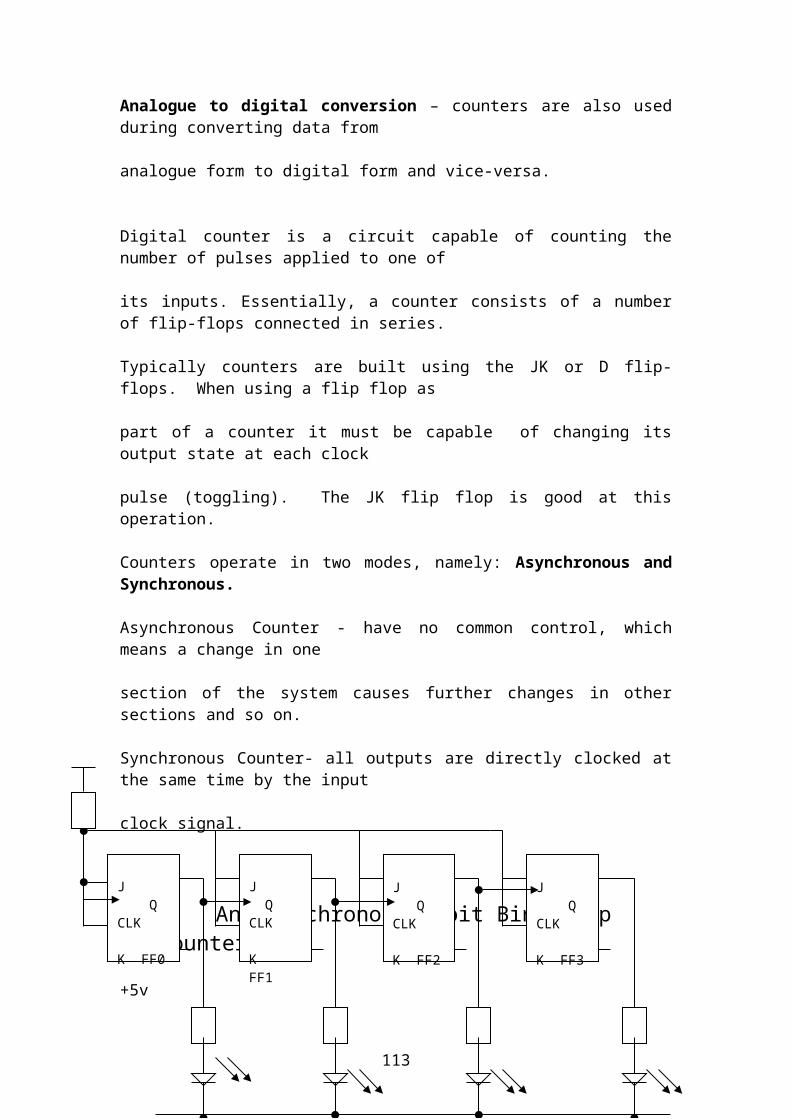
Question 1
a) Convert the decimal number 625.50 to :
BinaryOctal Hexadecimal (9 marks)
b) Complete the table below:
Decimal Unsigned Signed I’s complement 2’s complement Excess 4 (i) 3 011 011 ? ? ? (ii) 2 010 010 ? ? ? (iii) -2 - 110 ? ? ? (iv) -3 - 111 ? ? ?
(6 marks)Question 2
(a) Use logic gates and truth tables to show that:
(6 marks)
(b) Minimize the two Boolean functions below:
(15 marks)with don’t care terms 1,9,10,13
(c) Give at least four benefits derived from minimizing Boolean functions
(4 marks)
Question 3
Use the truth table below produce the:(i) logic equations in their minimal form(ii) the logic circuit diagram(iii) Explain the purpose of the circuit you have produced
Truth Table
113

Carry Out(COUT) Sum( S) Carry in(Cin) B A 0 0 0 0 0 0 1 0 0 1 0 1 0 1 0 1 0 0 1 1 0 1 1 0 0 1 0 1 0 1 1 0 1 1 0 1 1 1 1 1
Question 4
Design (fully) a clocked sequential circuit that goes through a sequence of repeated binary states 000,001,010,011,100,101,111,000,001, etc when an external input x is equal to 1. The state of the sequential circuit remains unchanged when the external input x = 0.
(25 marks)
Question 5
Design a BCD to seven-segment decoder. The decoder has a 4-bit natural BCD input represented by DCBA where A is the least significant bit. Assume that the BCD input can never be greater than nine (9). When one of its seven outputs (a to g) is true, the corresponding segment of the display is illuminated.
(25 marks)
114

SAMPLE PAST EXAMINATION PAPER 2 MODEL ANSWERS
Question 1
We convert 625.50 to binary by first converting the whole number part (625) using the remainder theorem and the fraction part(.50) using the multiplication method.
625/2 = 312 R 1 LSB312/2 = 156 R 0156/2 = 78 R 078/2 = 39 R139/2 = 19 R119/2 = 9 R1 9/2 = 4 R1 4/2 = 2 R0 2/2 = 1 R0 1/2 = 0 R1 MSB
62510 = 10011110012
We convert 0.50 to binary
0.50 x 2 = 1.00 MSB0.00 x 2 = 0.00 LSB
So 625.5010 = 1001111001.102
We convert the binary number 10011110012 to Octal decimal
001 001 111 001
1 2 7 18
We convert 0.102 to Octal decimal fraction
.102 = .1008
So 1001111001.102 = 1271.48
We convert the binary number 10011110012 to Hexadecimal
0010 0111 1001
2 7 516
We convert 0.102 to Hexadecimal fraction
.102 = .1000 = 816
115

So 1001111001.102 = 275.816
b) Complete the table below:
Decimal Unsigned Signed I’s complement 2’s complement Excess 4 (i) 3 011 011 011 011 111 (ii) 2 010 010 010 010 110
(iii) -2 - 110 101 110 010
(iv) -3 - 111 100 101 001
c) Convert 35810 to Hexadecimal Floating Point representation
Step 1: Convert the fixed point number from its original base into a fixed point
number in the target base.. We will use the remainder theorem.
Original base Integer Remainder
358/16 22 6 LSB
22/16 1 6
1/16 0 1 MSB
So (358) 10 = (166) 16
Step 2: Convert the fixed-point number to floating point number
(166) 16 = (166.) 16 x 160
Step 3: Normalise the number, for example
(166.) 16 x 160 = (.166) 16 x 163
Step 4: write the bit fields of the number. The number is positive so in the sign bit
position write a zero(0). The exponent is 3 but should be represented as excess-4, so
the bit pattern for the exponent is calculated as follows;
116

011(+3)10
Exceaa-4 = 011+100 = 111
Step 5: Each of the base 16 digits is represented in binary as 1=0001, 6= 0110 and
another 6 = 0110.
0 111 0001 0110 0110
+(sign) (exponent) (1) (6) (6)
The bit pattern is stored in the computer’s memory as 0111000101100110
Convert (9.375 x10⁻²) to base 2 scientific notation
Step 1: Convert from base 10 floating point to base 10 fixed point by moving the
decimal point two places to the left.
Step 2: Convert from base 10 fixed point to base 2 fixed point using the
multiplication method.
Step 3: Convert to normalised base 2 floating point
We follow all the steps to solve the problem
9.375 x 10-2 = .09375
.09375 x 2 = 0.1875
.1875 x 2 = 0.375
.375 x 2 = 0.75
75 x 2 = 1.5
5 x 2 = 1.0
(.09375) 10 = (.00011) 2
.00011 = .00011x 20
= 1.1 x 2-4
Question 2
117

Logic gate and truth table
Truth Table
X Y F
0 0 0
0 1 1
1 0 1
1 1 0
A
TRUTH TABLE
A B F The two truth tables are the same.0 0 0 0 1 11 0 11 1 0
118
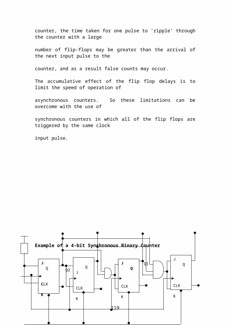
AA
TRUTH TABLE
X Y Z F0 0 0 00 0 1 00 1 0 00 1 1 01 0 0 01 0 1 01 1 0 01 1 1 1
TRUTH TABLE
X Y Z F0 0 0 00 0 1 00 1 0 00 1 1 01 0 0 01 0 1 01 1 0 01 1 1 1
The two truth tables are the same.
119

TRUTH TABLE
X1 X2 F0 0 00 1 11 0 1
1 1 1
TRUTH TABLE
X1 F0 01 1
Minimise the two function
AB 00 01 11 10 CD 00 1 1 1 1
01 1 1 11
10 1
AB 00 01 11 10 CD 00 1 1 1
01 x x
120
1 1
1 1
1 1
1 1
1 1
1
x
1
x
x

11 1 1 1
10 1 1 1 x
c) Benefits of minimising Boolean functions
(i) saving costs
(ii) reducing propagation delays
(iii) circuit simplification
(iv) improves productivity
Question 3
Truth Table
Carry Out(COUT) Sum( S) Carry in(Cin) B A 0 0 0 0 0 0 1 0 0 1 0 1 0 1 0 1 0 0 1 1 0 1 1 0 0 1 0 1 0 1 1 0 1 1 0 1 1 1 1 1
From the truth table, we derive the logic equations for building the
full adder circuit as follows:
121
From the Sum and Carryout logic equation we produce the circuit diagram.
The circuit above is called a Full Adder and is used for carrying out additions in
digital computer systems
Question 4
We follow the full design steps used in developing digital logic sequential circuitsStep 1
We produce the sequential sate diagram showing the specified operations of the
122

sequential circuit.
X = 1
X =1 X =1
X =1 X =1
X =1 x =1
X =1
Step 2
From the state diagram we produce the excitation table
Present State Input
Next State
Flip Flop Inputs
A B C X A B C JA KA JB KB JC KC0 0 0 0 0 0 0 0 x 0 x 0 x0 0 0 1 0 0 1 0 x 0 x 1 x0 0 1 0 0 0 1 0 x 0 x x 00 0 1 1 0 1 0 0 x 1 x x 10 1 0 0 0 1 0 0 x x 0 0 x0 1 0 1 0 1 1 0 x x 0 1 x0 1 1 0 0 1 1 0 x x 0 x 00 1 1 1 1 0 0 1 x x 1 x 11 0 0 0 1 0 0 x 0 0 x 0 x1 0 0 1 1 0 1 x 0 0 x 1 x1 0 1 0 1 0 1 x 0 x 1 x 01 0 1 1 1 1 0 x 0 1 x x 11 1 0 0 1 1 0 x 0 x 0 0 x1 1 0 1 1 1 1 x 0 x 0 1 x1 1 1 0 1 1 1 x 0 x 0 x 01 1 1 1 0 0 0 x 1 x 1 x 1
From the excitation table, we produce the logical equation used to construct the
123
00000
001
010
011
100
101
110
111
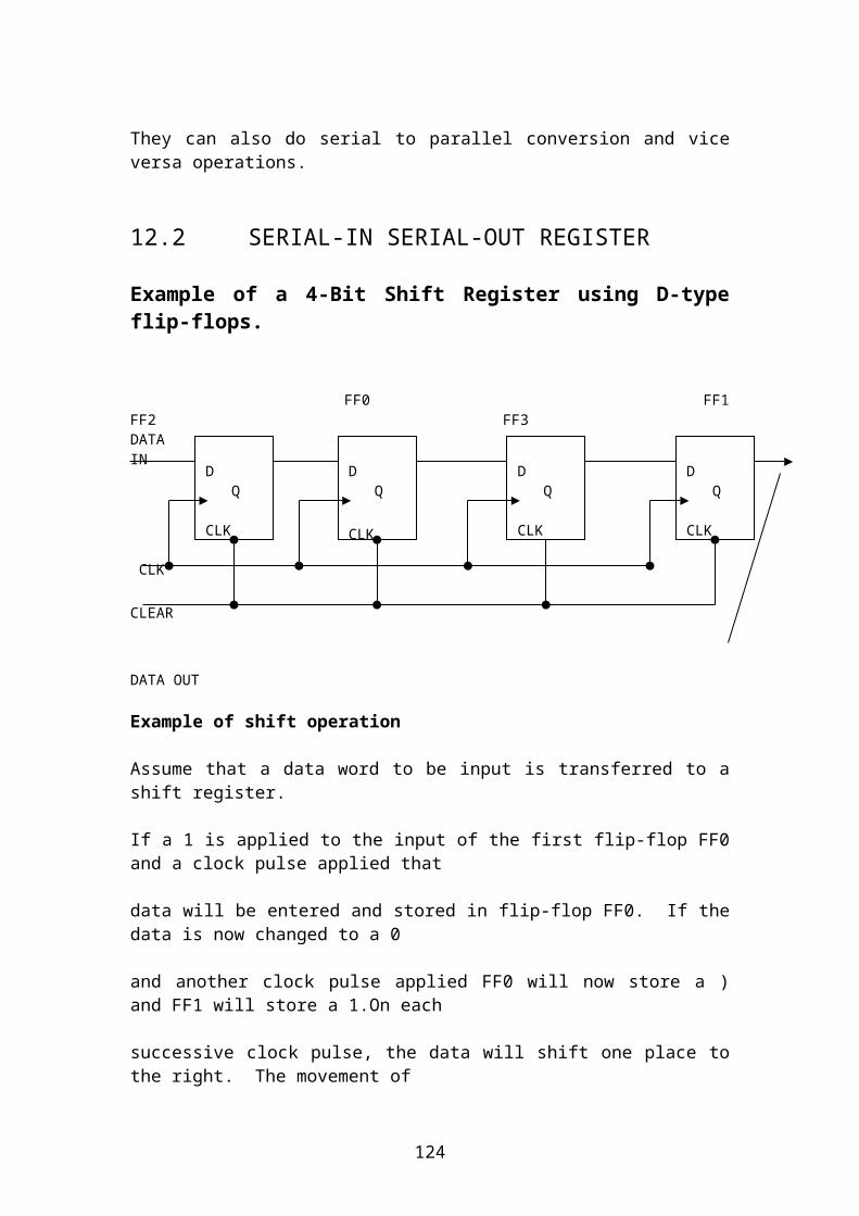
sequential circuit. Wee use the four variable Karnaugh map to minimise the functions
JA, KA, JB,KB and JC, KC.
AB 00 01 11 10 CX x x 00 01 x x
11 1 x x
10 x
AB 00 01 11 10 CX x x x 00 01 x x
11 11
10 x x
AB 00 01 11 10 CX 00 x 01 1 1 1 1
11 x x x x 10 x x x x
124
1 x
1 x x 1
1 1 1 1
x x x x

From the logic equations we produce the circuit A
X A
B
B
C
C
CLOCK
Question 5
D, C, B and A are the inputs to the binary coded decimal decoder.
The outputs a, b, c, d, e, f and g are produced from the seven-segment display
(see figure1 below)
a
f b
125
J Q
CLK
K
J Q
CLK
K
J Q
CLK
K
AND
AND
g

e c
d
Dec D C B A a b c d e f g0 0 0 0 0 1 1 1 1 1 1 01 0 0 0 1 0 1 1 0 0 0 02 0 0 1 0 1 1 0 1 1 0 13 0 0 1 1 1 1 1 1 0 0 14 0 1 0 0 0 1 1 0 0 1 15 0 1 0 1 1 0 1 1 0 1 16 0 1 1 0 1 0 1 1 1 1 17 0 1 1 1 1 1 1 0 0 0 08 1 0 0 0 1 1 1 1 1 1 19 1 0 0 1 1 1 1 1 0 1 110 1 0 1 0 x x x x x x x11 1 0 1 1 x x x x x x x12 1 1 0 0 x x x x x x x13 1 1 0 1 x x x x x x x14 1 1 1 0 x x x x x x x15 1 1 1 1 x x x x x x x
DC BA 00 01 11 10
00 1 0 x 101 0 1 x 1
11 1 1 x x
10 1 1 x x
This logic equation displays the a segment in the seven-
segment display circuit built using don’t care conditions.
126
x 1 1 1 x
1 1 x x
1 x
1 x

DC BA 00 01 11 10
00 1 1 x 1 01 x 1
11 1 1 x x
10 1 0 x x
This logic equation displays the b segment in the seven-
segment display circuit built using don’t care conditions.
DC BA 00 01 11 10
00 1 1 x 1
01 111 1 1 x x
10 0 1 x x
This logic equation displays the c segment in the seven-
segment display circuit built using don’t care conditions.
DC BA 00 01 11 10
00 1 0 x 1
01 0 x11 1 0 x x
10 1 1 x xx
This logic equation displays the d segment in the seven-
segment display circuit built using don’t care conditions.
127
1 1 x x
1 1 x 1
1 1 x 1
1 1 x 1 11 1 x 1
1 1 x x
1
1 x
1 x
1 x
1 x
x 1
x 1
1 1 x x x

DC BA 00 01 11 10
00 1 0 x 1 01 0 0 x x
11 0 0 x x
10 1 1 x x
This logic equation displays the e segment in the seven-
segment display circuit built using don’t care conditions.
DC BA 00 01 11 10
00 11 1 x 11
01 0
11 0 1 x x
10 0 x x x
This logic equation displays the f segment in the seven-
segment display circuit built using don’t care conditions We construct the logic circuit from the logic equations. SAMPLE PAST EXAMINATION PAPER 3
MIDLANDS STATE UNIVESITY
DEPARTMENT OF COMPUTER SCIENCE AND INFORMATION SYSTEMS
DIGITAL LOGIC DESIGN CODE HCS 103
128
1 1 x x
1
1
x
x
1 1 x 1
1 x
1 x

TIME 3 HOURS
INSTRUCTIONS TO CANDIDATES
This paper consists of six (6) questions on three (4) printed pages
ANSWER ALL QUESTIONS IN SECTION ONE AND ONE QUESTION IN SECTION TWO
Each question carries 20marks
SECTION ONE
Question 1
a) Convert the decimal number 19710 to Binary using:(i) The remainder theorem (ii) Binary Exponential Placeholders method (6 marks)
b) Convert (+506) and (-506) BCD to:(i) Nines and Tens Complement(ii) Nines complement (Negative) (4 marks)(iii) Tens complement (Negative)
129

c) . Use the Boolean properties below to minimize this function:
(i) Distributive(ii) Complement (10 marks)(iii) Indempotence(iv) Identity
Question 2
a) Use the full adder circuit above to produce its:(i) Truth table (10 marks)(ii) Logic equations (in their minimal form) used to build this circuit (10 marks)
Question 3
130

(a) Identify the above logic circuit (2 marks)(b) Produce its truth table (8 marks)(c produce the Boolean equation for F and verify it for all the inputs, D0 – D3 (10 marks)
Question 4
Design a circuit, which simulates the sequence of lights that occur on Gweru traffic lights. The circuit should have three inputs (connected to three separate switches), and three light emitting diodes (LEDS) according to the truth table below. Use Karnaugh map design technique to produce the Boolean logic expressions.
(20 marks)
SECTION TWO
Question 5
131

Present State Input
Next State
Flip Flop Inputs
A B C X A B C JA KA JB KB JC KC0 0 0 0 0 0 00 0 0 1 0 0 10 0 1 0 0 0 10 0 1 1 0 1 00 1 0 0 0 1 00 1 0 1 0 1 10 1 1 0 0 1 10 1 1 1 1 0 01 0 0 0 1 0 01 0 0 1 1 0 11 0 1 0 1 0 11 0 1 1 1 1 01 1 0 0 1 1 01 1 0 1 1 1 11 1 1 0 1 1 11 1 1 1 0 0 0
a) From the state table above, produce an excitation table (10 marks)
b) From the excitation table in (a) produce logic equations for JA, KA, JB,
c) KB and JC, KC (5 marks)
d) From the logic equations in (b) produce the logic circuit and verify its
e) operations (5 marks)
Question 6
The circuit diagram below is a typical sequential circuit
a) (i) Name the components of this sequential circuit
132

(ii)Use this sequential circuit to produce the equations, DA, BD and the state
the state equation Y
b) Use this circuit to produce the state table showing the operations of the
c) sequential circuit
d) From the state table produce the corresponding state diagram
A
B
CLOCK
Y
133
Q
DC
D Q
C
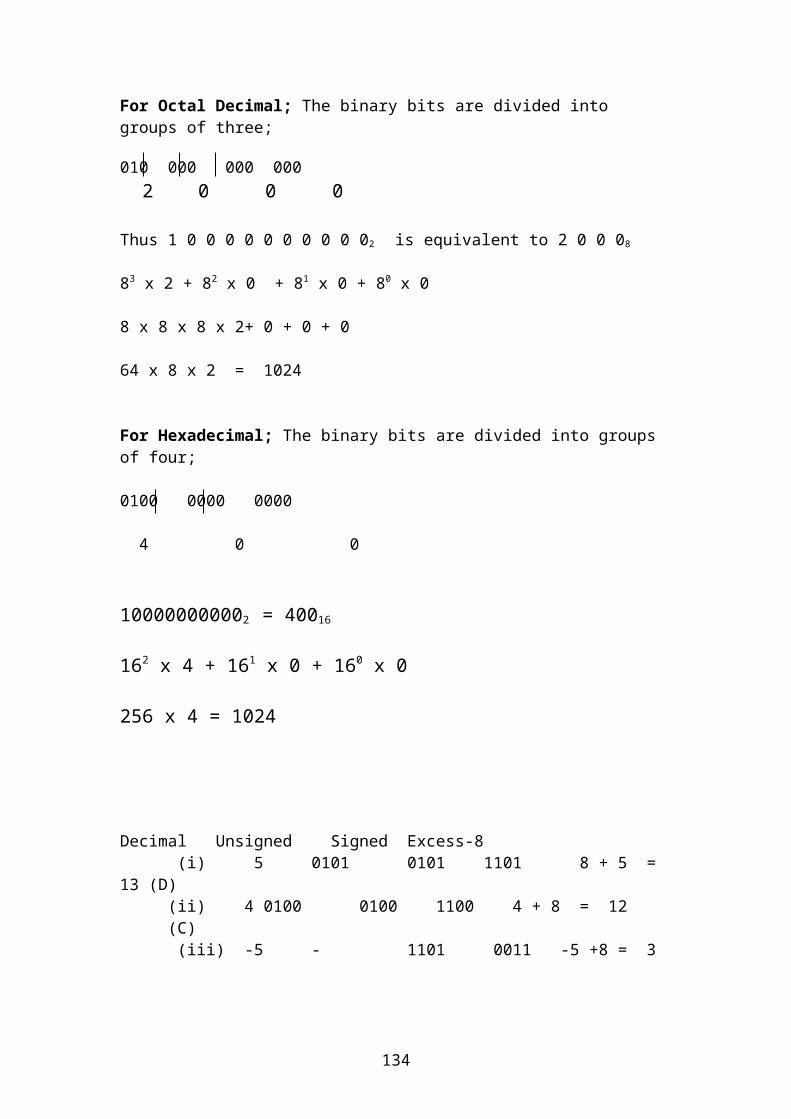
SAMPLE PAST EXAMINATION PAPER 3 MODEL ANSWERS
Question 1
Using the remainder theorem/division method
i) 197/2 = 98 R 1 LSB 98/2 = 49 R 0 49/2 = 24 R 1 24/2 = 12 R 0 12/2 = 6 R 0 6/2 = 3 R 0 3/2 = 1 R 1 1/2 = 0 R 1 MSB
19710 = 110001012
ii)
Using the Binary Exponential Placeholders
The highest Binary Exponential Placeholders next to 127 is 128, which is 27. If 128
can be subtracted from 128, we write a 1 in column 128, Subtract 128 from 197. The
answer is 69. If 64 can be subtracted from 69, we put a 1 in column in 64. We subtract
64 from 69. The answer is 5. 32 cannot be subtracted from 5. We put a zero (0) in
column 32. Next is column is 8, which cannot be subtracted from 5 and we put a 0 in
column 8. Next is column 4. 4 can be subtracted from 5, so we put a 1 in column 4.
Subtract 4 from 5 and the answer is 1. Next column is 2 and 2 cannot be subtracted
from 1 and we write a 0 in column 2. Next column is 1 and 1 can be subtracted from
1, so we put a 1 in column 1.
Positional weight 27 26 25 24 23 22 21 20
134

Value 128 64 32 16 8 4 2 1
Number 1 1 0 0 0 1 0 1
So we have 1 1 0 0 0 1 0 12 = 19710
We prove this by converting 11000101 back to decimal.
27 x 1+ 26x1+25x 0+24x 0+23x 0 +22x1+21x0+20x1
= 128+64+4++1=197
b)
(+506)
0000 0101 0000 0110(+) 5 0 6 Nines and Tens complement (positive)
(-506)
1001 0100 1001 0011(-) 4 9 3 Nines complement (Negative)
1001 4 9 3 + 1
1001 0100 1001 0100 Tens complement (Negative)
. The properties of Boolean algebra can be used to
reduce the equation.
Distributive property (1)
Complement property (2)
Identity property (3)
We can reduce equation 3 by introducing the property Idempotence and re-
introducing ABC, for example:
Idempotence (4) Distributive (5)
135

Identity (6)
We can also re-introduce ABC to equation 6, for example
Idempotence (7)
Distributive (8)
Identity (9)
Question 2
The truth table can be produced by tracing signal lowing from inputs A,B , Cin . Since
we have thee inputs, all possible combinations range from 000-111.
Carry Out(COUT) Sum( S) Carry in(Cin) B A 0 0 0 0 0 0 1 0 0 1 0 1 0 1 0 1 0 0 1 1 0 1 1 0 0 1 0 1 0 1 1 0 1 1 0 1 1 1 1 1
From the truth table, we can obtain the logic equations for SUM(S) and
Carryout(Cout). And reduce these to their minimal forms.
Question 3
The circuit is a Mult iplexer
Truth Table
136

S1 S2 F
0 0 D0
0 1 D1
1 0 D2
1 1 D3
Proof of the Boolean function (F)
D0.1.1+D1.1.0+D2.0.1+D3.0.0
D01.1+0+0+0 = D0
D0.0.1+D1.1+D2.1.0+D3.0.0
0+D1.1.1+0+0 = D1
D0.0.0+D1.0.1+D2.1.1+D3.0.0
0+0+D2.1.1+0 = D2
D0.0.1+ D1.1.0+D2.0.0+D3.1.1
0+0+0+D3.1.1 = D3
Question 4
S0S1 S2 00 01 11 10
0 1 1 1 1
1
S0S1 S2 00 01 11 10
137
1 1 1 1

0 1
1 1
S0S1 S2 00 01 11 10
0
1 1 1 1
From the logic equations we produce the logic circuit
Question 5
From the state diagram we produce the excitation table
Present State Input
Next State
Flip Flop Inputs
A B C X A B C JA KA JB KB JC KC0 0 0 0 0 0 0 0 x 0 x 0 x0 0 0 1 0 0 1 0 x 0 x 1 x0 0 1 0 0 0 1 0 x 0 x x 00 0 1 1 0 1 0 0 x 1 x x 10 1 0 0 0 1 0 0 x x 0 0 x0 1 0 1 0 1 1 0 x x 0 1 x0 1 1 0 0 1 1 0 x x 0 x 00 1 1 1 1 0 0 1 x x 1 x 11 0 0 0 1 0 0 x 0 0 x 0 x1 0 0 1 1 0 1 x 0 0 x 1 x1 0 1 0 1 0 1 x 0 x 1 x 0
138
1
1
1 1
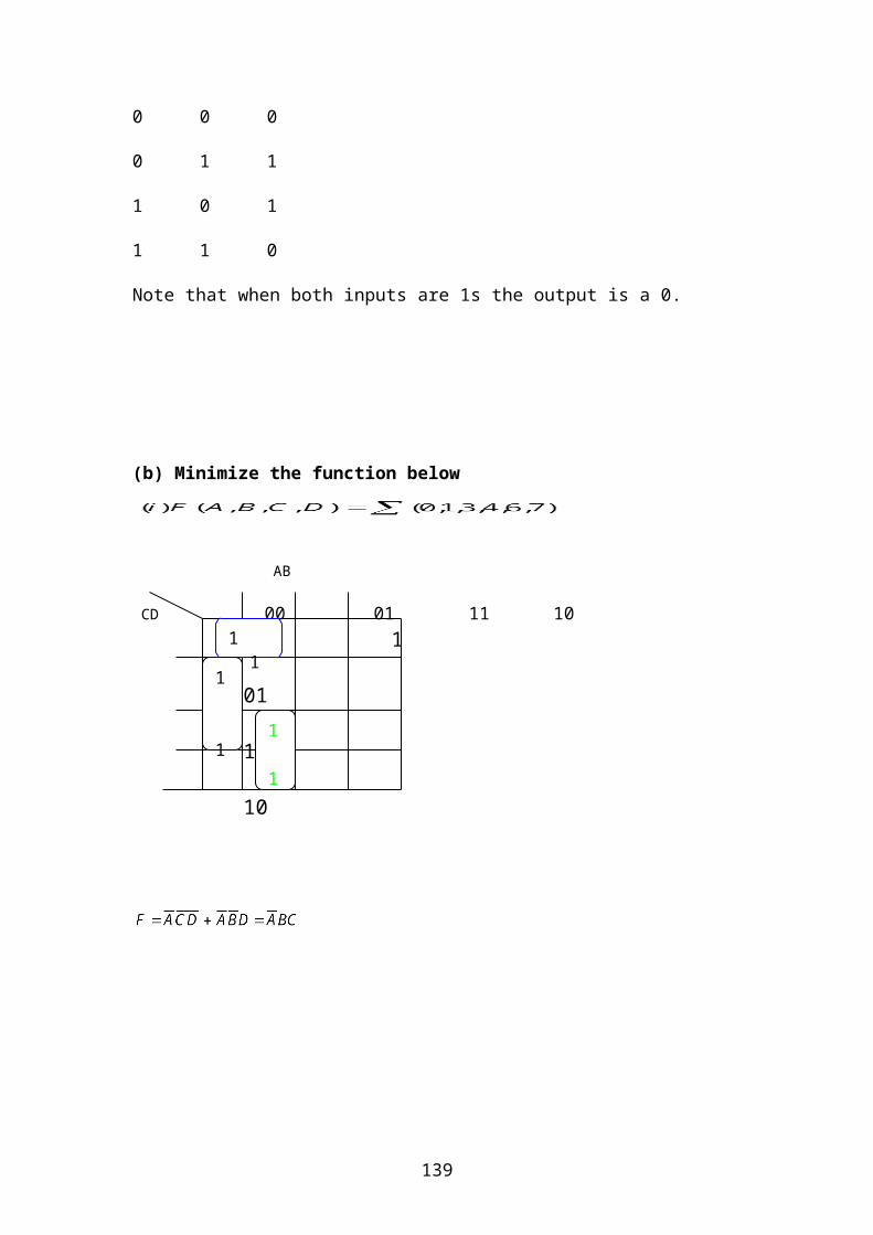
1 0 1 1 1 1 0 x 0 1 x x 11 1 0 0 1 1 0 x 0 x 0 0 x1 1 0 1 1 1 1 x 0 x 0 1 x1 1 1 0 1 1 1 x 0 x 0 x 01 1 1 1 0 0 0 x 1 x 1 x 1
From the excitation table, we produce the logical equation used to construct the sequential circuit. Wee use the four variable Karnaugh map to minimise the functions JA, KA, JB,KB and JC, KC.
AB 00 01 11 10 CX x x 00 01 x x
11 1 x x
10 x
AB 00 01 11 10 CX x x x 00 01 x x
11 11
10 x x
AB 00 01 11 10 CX 00 x 01 1 1 1 1
11 x x x x
139
1 x
1 x x 1
1 1 1 1
x x x x

10 x x x x
From the logic equations produce the circuit A
X A
B
B
C
C
CLOCKQuestion 6
The components of the sequential circuit are:
(i) the combinational logic part, made up of the AND gates, OR gates and the
(ii) INVERTER(NOT gate) and the storage part, made up of the two D flip
flops.
(iii) (A and B are the outputs of the two flip flops and x is the external input)
140
J Q
CLK
K
J Q
CLK
K
J Q
CLK
K
AND
AND

(this equation is derived from the single And gate whose output
is connected to the D input of the flip flop B
(state equation)
b)
This state table is produced by using the present state of flip flops A and B, and
external input X as our inputs to the sequential circuit.
State table of the sequential circuit Present State Input Next State Output
A B X A B Y
0 0 0 0 0 0
0 0 1 0 1 0
0 1 0 0 0 1
0 1 1 1 1 0
1 0 0 1 0 1
1 0 1 1 0 0
1 1 0 0 0 1
1 1 1 1 0 0
The information in a state table can be represented graphically in a state diagram as shown below.
0/0
0/1 1/0
0/1
141
00
10
01
11

1/00/1 1/0
REFERENCES
Brown S D, Fundamentals of Digital Logic Design
Published by McGraw Hill (1999), India
Floyd, T, L, Digital Fundamentals
Published by Prentice Hall International (2000), New Jersey
Hamacher Carl, Zvonko Vranesic, Computer Organization
Published by McGraw Hill (1990), India
142

Cripps, Martin, Introduction to computer hardware
Published by Winthrop Publishers (1989), Cambridge
Morris, Mano, Computer Systems Architecture
Published by Kluwer International Series (1997), California
Hanley T, Microprocessors and Microcomputer Technology
Published by BPB Publishers(1993), India
Holds worth B, Digital Logic Design
Published by Butterworth (1982)
Roth C, H, Fundamentals of Logic Design
Published by West Publishing (1995)
Wakerly, F, J, Digital Design principles
Published by West Publishers (1995)
Gajski, D, D, Principles of Digital Design
Published by Prentice Hall (1997), New Jersey
Mano, M and Kune, R, K, Logic and Computer Design Fundamentals
Published by Prentice Hall (1997), New Jersey
Uyemura, John, Logic Circuit Design
Published by Kluwer Academic Publishers (1999), California
143