Embed Size (px)
Citation preview
Practical Digital Pre-Distortion
Techniques for PA Linearization
in 3GPP LTE
Copyright Agilent Technologies 2010SystemVue DPD
Jinbiao XU
May 26, 20101
Jinbiao Xu
Agilent Technologies
Master System Engineer
Agenda
• Digital PreDistortion----Principle
• Crest Factor Reduction
• Digital PreDistortion Simulation
• Digital PreDistortion Hardware Verification
Copyright Agilent Technologies 2010SystemVue DPD
Jinbiao XU
May 26, 20102
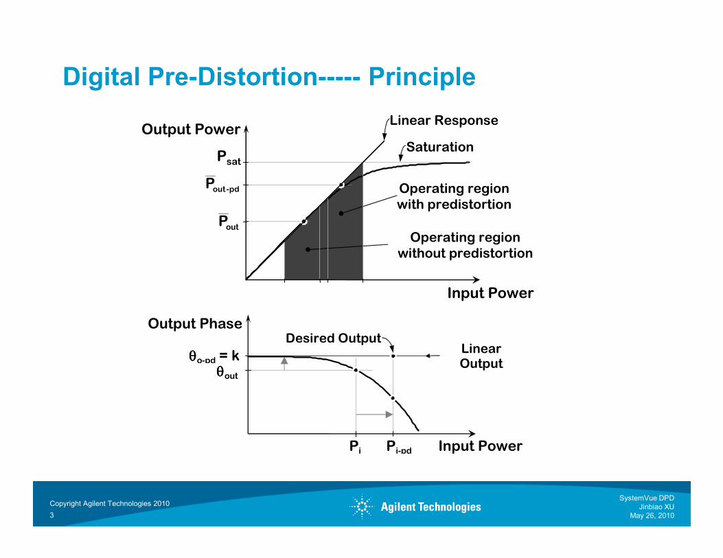
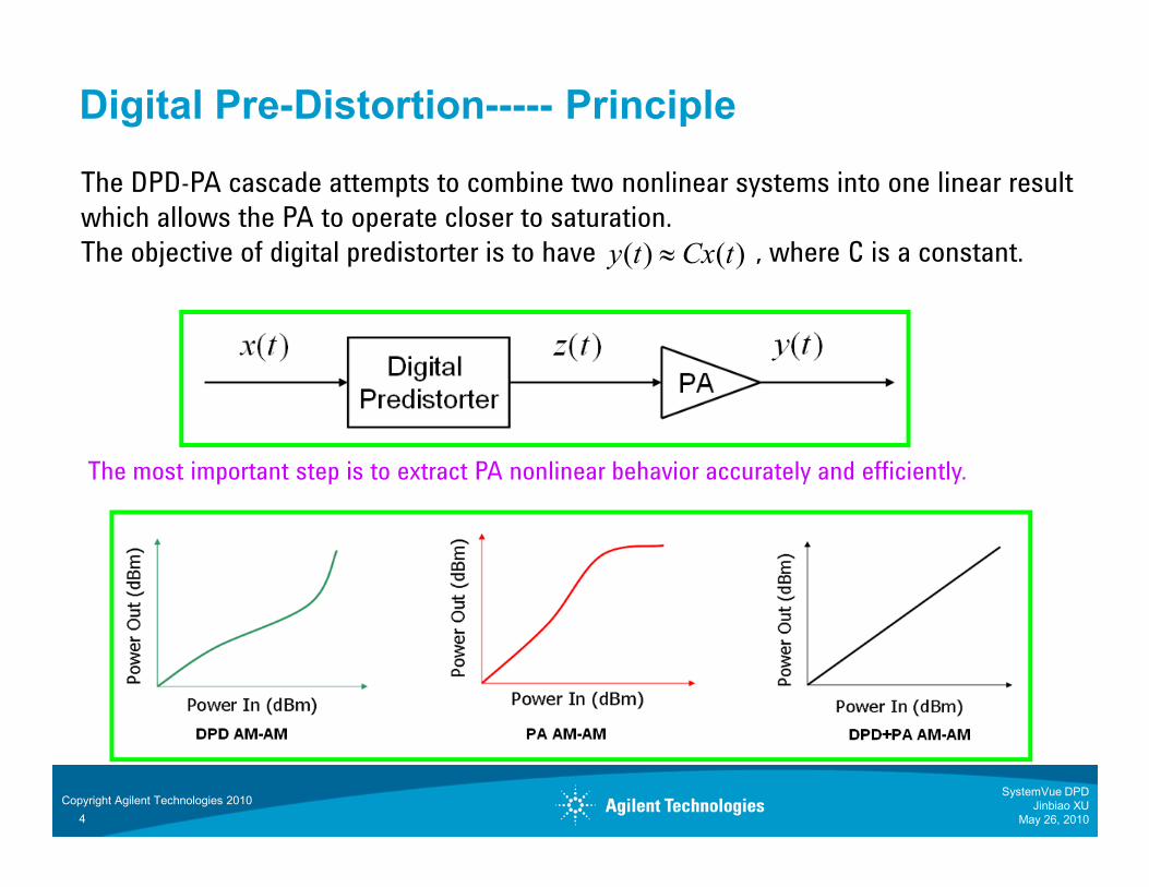
Digital Pre-Distortion----- Principle
outP
Linear ResponseOutput Power
SaturationPsat
pd-outP Operating region
with predistortion
Operating region
without predistortion
Input Power
θθθθo-pd = k θθθθout
Input Power
Output Phase
Pi Pi-pd
Desired Output Linear Output
Copyright Agilent Technologies 2010SystemVue DPD
Jinbiao XU
May 26, 20103
Digital Pre-Distortion----- Principle
The DPD-PA cascade attempts to combine two nonlinear systems into one linear result
which allows the PA to operate closer to saturation.
The objective of digital predistorter is to have , where C is a constant.)()( tCxty ≈
4
Copyright Agilent Technologies 2010SystemVue DPD
Jinbiao XU
May 26, 2010
The most important step is to extract PA nonlinear behavior accurately and efficiently.
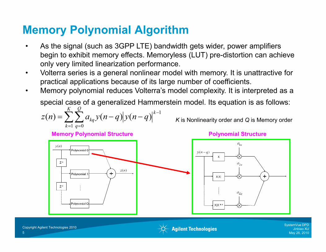
Memory Polynomial Algorithm
• As the signal (such as 3GPP LTE) bandwidth gets wider, power amplifiers
begin to exhibit memory effects. Memoryless (LUT) pre-distortion can achieve
only very limited linearization performance.
• Volterra series is a general nonlinear model with memory. It is unattractive for
practical applications because of its large number of coefficients.
• Memory polynomial reduces Volterra’s model complexity. It is interpreted as a
special case of a generalized Hammerstein model. Its equation is as follows:
K is Nonlinearity order and Q is Memory order∑∑= =
−−−=
K
k
Q
q
k
kq qnyqnyanz1 0
1)()()(
Copyright Agilent Technologies 2010
5
Memory Polynomial Structure Polynomial Structure
SystemVue DPD
Jinbiao XU
May 26, 2010
= =k q1 0
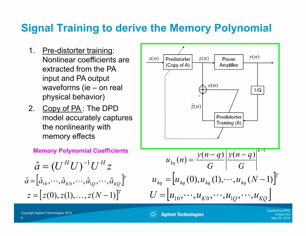
Signal Training to derive the Memory Polynomial
1. Pre-distorter training:
Nonlinear coefficients are
extracted from the PA
input and PA output
waveforms (ie – on real
physical behavior)
2. Copy of PA : The DPD
model accurately captures model accurately captures
the nonlinearity with
memory effects
Copyright Agilent Technologies 2010
6
zUUUa HH 1)(ˆ −=
[ ]TNzzzz )1(,),1(),0( −= K [ ]KQQK uuuuU ,,,,,, 1010 LLL=
[ ]Tkqkqkqkq Nuuuu )1(,),1(),0( −= L
1)()(
)(
−−−
=
k
kqG
qny
G
qnynu
Memory Polynomial Coefficients
[ ]TKQQK aaaaa ˆ,,ˆ,,ˆ,,ˆˆ1010 LLL=
SystemVue DPD
Jinbiao XU
May 26, 2010
• Spectrally efficient wideband RF signals may have PAPR >13dB.
• CFR preconditions the signal to reduce signal peaks without significant
signal distortion
• CFR allows the PA to operate more efficiently – it is not a linearization
technique
• CFR supplements DPD and improves DPD effectiveness
• Without CFR and DPD, a basestation PA must operate at significant
back-off from saturated power to maintain linearity. The back-off
Crest Factor Reduction (CFR) Concepts
back-off from saturated power to maintain linearity. The back-off
reduces efficiency
Benefits of CFR
1. PAs can operate closer to saturation, for improved efficiency (PAE).
2. Output signal still complies with spectral mask and EVM specifications
Copyright Agilent Technologies 2010
7
SystemVue DPD
Jinbiao XU
May 26, 2010
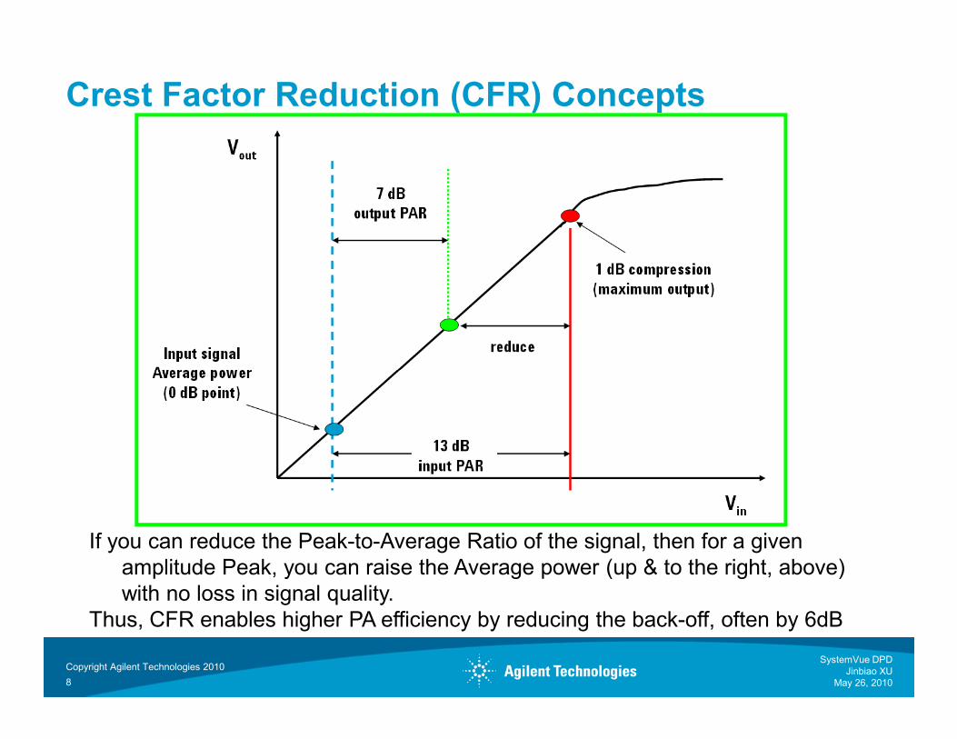
Crest Factor Reduction (CFR) Concepts
If you can reduce the Peak-to-Average Ratio of the signal, then for a given
amplitude Peak, you can raise the Average power (up & to the right, above)
with no loss in signal quality.
Thus, CFR enables higher PA efficiency by reducing the back-off, often by 6dB
Copyright Agilent Technologies 2010
8
SystemVue DPD
Jinbiao XU
May 26, 2010
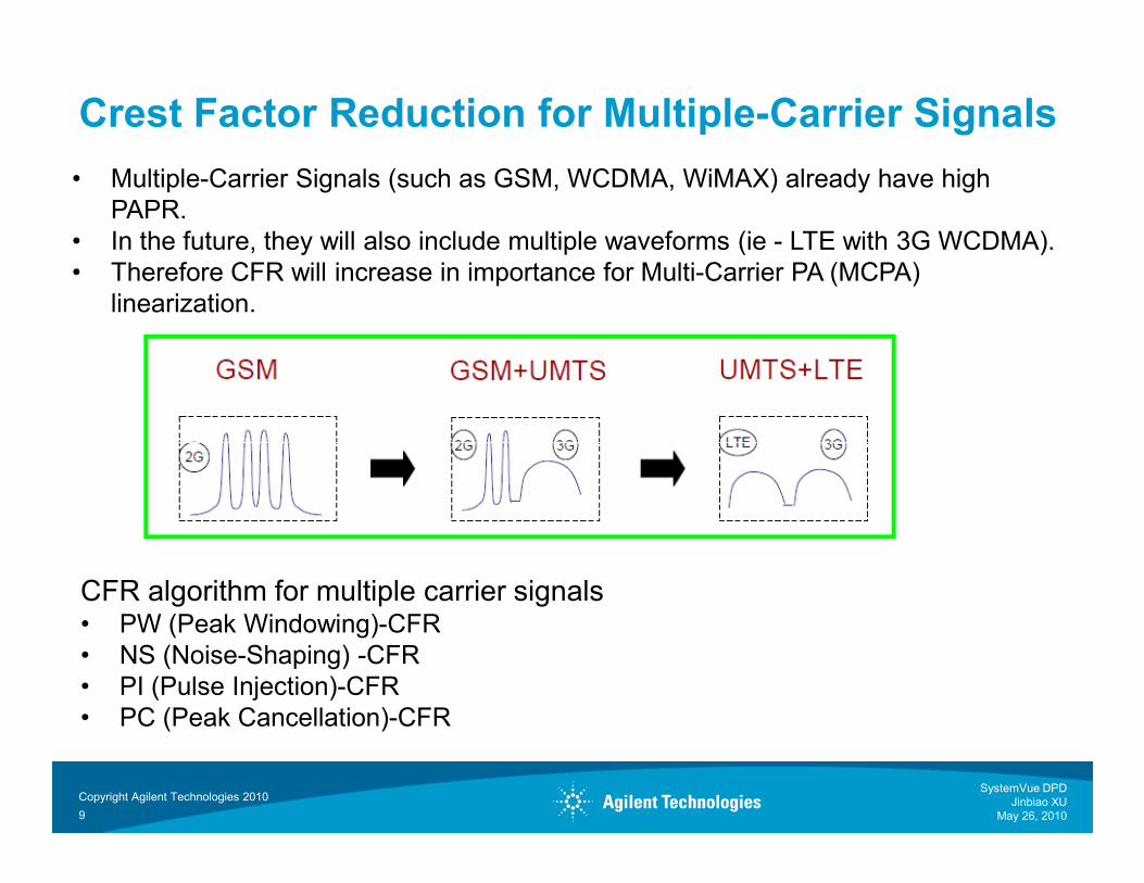
Crest Factor Reduction for Multiple-Carrier Signals
• Multiple-Carrier Signals (such as GSM, WCDMA, WiMAX) already have high
PAPR.
• In the future, they will also include multiple waveforms (ie - LTE with 3G WCDMA).
• Therefore CFR will increase in importance for Multi-Carrier PA (MCPA)
linearization.
Copyright Agilent Technologies 2010
9
CFR algorithm for multiple carrier signals• PW (Peak Windowing)-CFR
• NS (Noise-Shaping) -CFR
• PI (Pulse Injection)-CFR
• PC (Peak Cancellation)-CFR
SystemVue DPD
Jinbiao XU
May 26, 2010
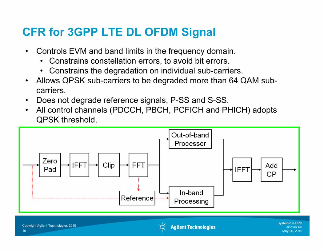
CFR for 3GPP LTE DL OFDM Signal
• Controls EVM and band limits in the frequency domain.
• Constrains constellation errors, to avoid bit errors.
• Constrains the degradation on individual sub-carriers.
• Allows QPSK sub-carriers to be degraded more than 64 QAM sub-
carriers.
• Does not degrade reference signals, P-SS and S-SS.
• All control channels (PDCCH, PBCH, PCFICH and PHICH) adopts
QPSK threshold.
Copyright Agilent Technologies 2010
10
SystemVue DPD
Jinbiao XU
May 26, 2010

LTE CFR (Crest Factor Reduction)
Simulation Results
FFT
FreqSequence=0-pos-neg
Direction=InverseSize=4096 [DFTSize]
FFTSize=4096 [DFTSize]ifft2
0+0*j
Value=0 [0+0* j]zeros
Gain=1
G3
Gain=1
G2
A
BlockSizes=1;300;3495;300 [[1,Half_UsedCarriers,DFT_zeros,Half_UsedCarriers]]
A3
A
BlockSizes=300;300 [[Half_UsedCarriers, Half_UsedCarriers]]
A2
FFT
FreqSequence=0-pos-neg
Direction=ForwardSize=4096 [DFTSize]
FFTSize=4096 [DFTSize]
fft
FFT
FreqSequence=0-pos-neg
Direction=InverseSize=4096 [DFTSize]
FFTSize=4096 [DFTSize]
ifft1
0+0*j
Value=0 [0+0* j]
DC
DPD_Rad ius Clip
input out put
ClippingThreshold=16.5e-6 [ClippingThreshold]
DPD_RadiusClip
DPD_LTE_CFR_Post Proc
input
ref
SC_St at us
Qm
out put
OutOfBandAlgorithm=Armstrong algorithm
EVM_Threshold_64QAM=0.1 [EVM_Threshold_64QAM]EVM_Threshold_16QAM=0.1 [EVM_Threshold_16QAM]
EVM_Threshold_QPSK=0.1 [EVM_Threshold_QPSK]
SSS_Ra=0 [SSS_Ra]PSS_Ra=0 [PSS_Ra]
UEs_Pa=0;0;0;0;0;0 [UEs_Pa]
PDSCH_PowerRatio=p_B/p_A = 1 [PDSCH_PowerRatio]PDCCH_Rb=0 [PDCCH_Rb]
PDCCH_Ra=0 [PDCCH_Ra]PBCH_Rb=0 [PBCH_Rb]
PBCH_Ra=0 [PBCH_Ra]
PHICH_Rb=0 [PHICH_Rb]PHICH_Ra=0 [PHICH_Ra]
PCFICH_Rb=0 [PCFICH_Rb]
RS_EPRE=-25 [RS_EPRE]OtherUEs_MappingType=0;0;0;0;0 [OtherUEs_MappingType]
UE1_MappingType=0;0;0;0;0;0;0;0;0;0 [UE1_MappingType]CyclicPrefix=Normal [CyclicPrefix]
OversamplingOption=Ratio 4 [OversamplingOption]
Bandwidth=BW 10 MHz [Bandwidth]D1
LTE Downlink 10MHz,
Sampling Rate 61.44MHz,
QPSK,
EVM threshold 10%
Simulation Results
Copyright Agilent Technologies 2010SystemVue DPD
Jinbiao XU
May 26, 201011
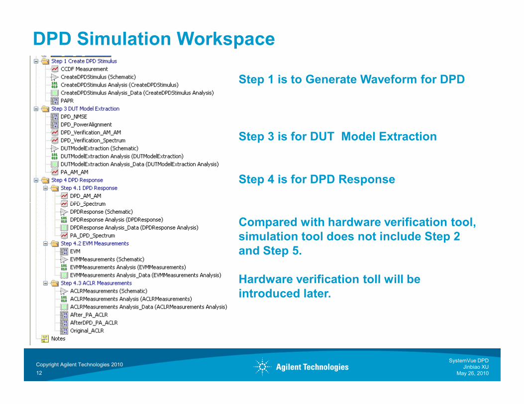
DPD Simulation Workspace
Step 1 is to Generate Waveform for DPD
Step 3 is for DUT Model Extraction
Step 4 is for DPD Response
Compared with hardware verification tool,
simulation tool does not include Step 2
and Step 5.
Hardware verification toll will be
introduced later.
Copyright Agilent Technologies 2010SystemVue DPD
Jinbiao XU
May 26, 201012
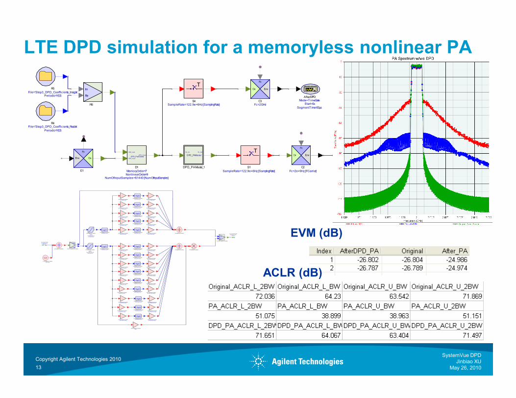
LTE DPD simulation for a memoryless nonlinear PA
MathPow10
FunctionType=Pow10
M12 {Math@Data Flow Models}
G28 {Gain@Data Flow Models} G23 {Gain@Data Flow Models}
DPD_PAModel
PA_IN PA_OUT
DPD_PAModel_1
T
SampleRate=122.9e+6Hz [SamplingRate]S4
Fc
EnvCx
Fc=2GHzC3
DPD_PreDistorterDPD_Input
DPD_Coef
DPD_Output
NumOfInputSamples=61440 [NumOfInputSamples]NonlinearOrder=9MemoryOrder=7
D1
Spectrum Analyzer
SegmentTime=50µs
Start=0sMode=TimeGate
AfterDPD
Fc
CxEnv
E1
Re
Im
R6
Periodic=YESFile='Step3_DPD_Coefficients_Imag.txt
R5
Periodic=YES
File='Step3_DPD_Coefficients_Real.txtR4
T
SampleRate=122.9e+6Hz [SamplingRate]
S1
Fc
EnvCx
Fc=2e+9Hz [FCarrier]
C2
Spectrum Analyzer
SegmentTime=50µsStart=0s
Mode=TimeGateAfterDPD_PA
Gain=0 [mPowers(1)]
G18 {Gain@Data Flow Models}
MathPow10
FunctionType=Pow10
M4 {Math@Data Flow Models}
MathPow10
FunctionType=Pow10
M5 {Math@Data Flow Models}
MathPow10
FunctionType=Pow10
M6 {Math@Data Flow Models}
MathPow10
FunctionType=Pow10
M7 {Math@Data Flow Models}
MathPow10
FunctionType=Pow10M8 {Math@Data Flow Models}
MathPow10
FunctionType=Pow10
M9 {Math@Data Flow Models}
MathPow10
FunctionType=Pow10
M10 {Math@Data Flow Models}
MathPow10
FunctionType=Pow10M11 {Math@Data Flow Models}
Gain=2 [mPowers(3)]
G16 {Gain@Data Flow Models}
Gain=1 [mPowers(2)]
G17 {Gain@Data Flow Models}
Gain=4 [mPowers(4)]G15 {Gain@Data Flow Models}
MathPow10
FunctionType=Pow10M3 {Math@Data Flow Models}
Gain=31.623 [mPars(1)]
G1 {Gain@Data Flow Models}
Gain=-72.068 [mPars(2)]
G2 {Gain@Data Flow Models}
Gain=254.726 [mPars(3)]
G3 {Gain@Data Flow Models}
Gain=-1107.963 [mPars(4)]G6 {Gain@Data Flow Models}
Gain=2956.358 [mPars(5)]
G5 {Gain@Data Flow Models}
Gain=-4462.485 [mPars(6)]
G4 {Gain@Data Flow Models}
Gain=3782.968 [mPars(7)]G9 {Gain@Data Flow Models}
Gain=-1653.647 [mPars(8)]
G8 {Gain@Data Flow Models}
Gain=281.85 [mPars(9)]
G7 {Gain@Data Flow Models}
A1 {Add@Data Flow Models}
MathPow10
FunctionType=Pow10M15 {Math@Data Flow Models}
FunctionType=Pow10
MathPow10
FunctionType=Pow10M13 {Math@Data Flow Models}
MathPow10
FunctionType=Pow10
M14 {Math@Data Flow Models}
MathPow10
FunctionType=Pow10
M16 {Math@Data Flow Models}
Gain=6 [pPowers(5)]
G25 {Gain@Data Flow Models}
Gain=4 [pPowers(4)]
G24 {Gain@Data Flow Models}
Gain=2 [pPowers(3)]
G27 {Gain@Data Flow Models}
Gain=1 [pPowers(2)]
G26 {Gain@Data Flow Models}
Gain=0 [pPowers(1)]G28 {Gain@Data Flow Models}
Gain=-1.159 [pPars(1)]G23 {Gain@Data Flow Models}
Gain=0.917 [pPars(2)]
G22 {Gain@Data Flow Models}
Gain=-1.746 [pPars(3)]
G21 {Gain@Data Flow Models}
Gain=0.992 [pPars(4)]
G20 {Gain@Data Flow Models}
Gain=-0.155 [pPars(5)]
G19 {Gain@Data Flow Models} A2 {Add@Data Flow Models}
Gain=14 [mPowers(9)]
G10 {Gain@Data Flow Models}
Gain=12 [mPowers(8)]
G11 {Gain@Data Flow Models}
Gain=10 [mPowers(7)]G12 {Gain@Data Flow Models}
Gain=8 [mPowers(6)]
G13 {Gain@Data Flow Models}
Gain=6 [mPowers(5)]
G14 {Gain@Data Flow Models}
Mag
Phase
C2 {CxToPolar@Data Flow Models}
MathLog10
FunctionType=Log10M17 {Math@Data Flow Models}
MathLog10
FunctionType=Log10M2 {Math@Data Flow Models}
LimiterType=linear
Top=0.788 [mXmaxVolt]
Bottom=0K=1
L2 {Limit@Data Flow Models}
LimiterType=linear
Top=0.86 [pXmaxVolt]
Bottom=0K=1
L3 {Limit@Data Flow Models}
M1 {Mpy@Data Flow Models}
Gain=1G29 {Gain@Data Flow Models}
Mag
Phase
P1 {PolarToCx@Data Flow Models}
Bus=NO
Data Type=Complex
PA_OUT {DATAPORT}
A3 {Add@Data Flow Models}
10e-201
Value=1e-200
C1 {Const@Data Flow Models}
Bus=NOData Type=Complex
PA_IN {DATAPORT}
EVM (dB)
ACLR (dB)
Copyright Agilent Technologies 2010SystemVue DPD
Jinbiao XU
May 26, 201013
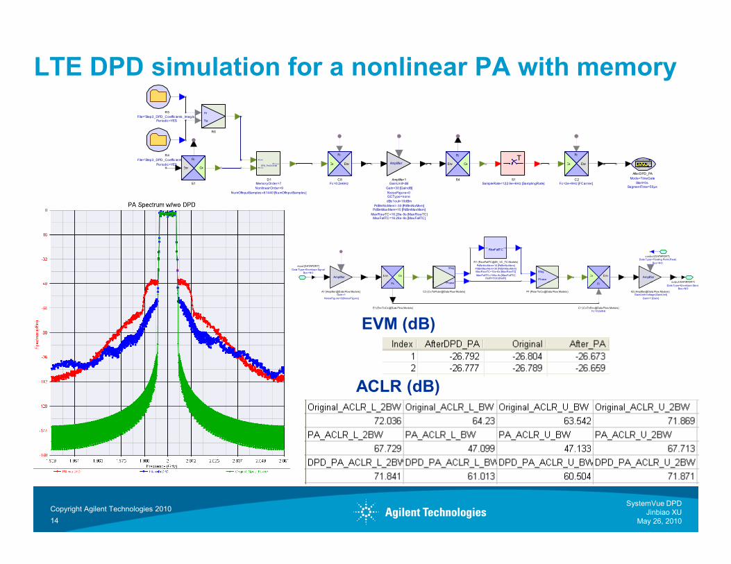
LTE DPD simulation for a nonlinear PA with memory
DPD_PreDis to rterDPD_I nput
DPD_Coef
DPD_O ut put
NumOfInputSamples=61440 [NumOfInputSamples]
NonlinearOrder=9
MemoryOrder=7
D1
Fc
CxEnv
E4
Amplifier
MaxFallTC=16.28e-9s [MaxFallTC]
MaxRiseTC=16.28e-9s [MaxRiseTC]
PdBmMaxMem=10 [PdBmMaxMem]
PdBmNoMem=-30 [PdBmNoMem]
dBc1out=10dBm
GCType=none
NoiseFigure=0
Gain=30 [GaindB]
GainUnit=dB
Amplifier1
T
SampleRate=122.9e+6Hz [SamplingRate]
S1
Fc
EnvCx
Fc=2e+9Hz [FCarrier]
C2
Spectrum Analyzer
SegmentTime=50µs
Start=0s
Mode=TimeGate
AfterDPD_PA
Fc
EnvCx
Fc=0.2e6Hz
C8
Re
Im
R6
Periodic=YES
File='Step3_DPD_Coeffic ients_Imag.tx t
R5
Periodic=YES
File='Step3_DPD_Coeffic ients_Real.tx t
R4
Fc
CxEnv
E1
Fc
CxEnv
Mag
Phase
Mag
Phase
Fc
EnvCx
Bus=NO
Data Type=Floating Point (Real)
control {DATAPORT}
output {DATAPORT}
Bus=NO
Data Type=Envelope Signal
input {DATAPORT}
RiseFallTCv in v out
RefR=50O [RefR]MaxFallTC=100e-6s [MaxFallTC]
MaxRiseTC=10e-6s [MaxRiseTC]PdBmMaxMem=30 [PdBmMaxMem]
PdBmNoMem=10 [PdBmNoMem]
R1 {RiseFallTC@SV_VC_TC Models}
Amplifier Amplifier
EVM (dB)
ACLR (dB)
Fc
E1 {EnvToCx@Data Flow Models}
Phase
C3 {CxToPolar@Data Flow Models} P1 {PolarToCx@Data Flow Models}
Fc
Fc=0.2e6Hz
C1 {CxToEnv@Data Flow Models}
Bus=NO
Data Type=Envelope Signal
output {DATAPORT}
NoiseFigure=0 [NoiseFigure]
Gain=1A1 {Amplifier@Data Flow Models}
Gain=1 [Gain]
GainUnit=voltage [GainUnit]A2 {Amplifier@Data Flow Models}
Copyright Agilent Technologies 2010SystemVue DPD
Jinbiao XU
May 26, 201014
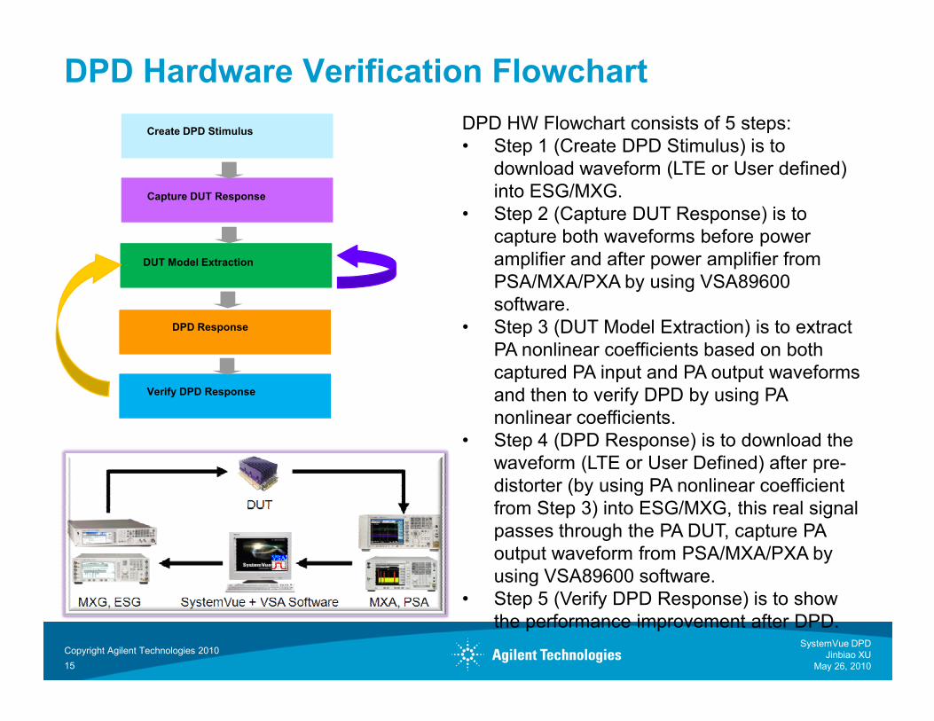
DPD Hardware Verification Flowchart
Create DPD Stimulus
Capture DUT Response
DUT Model Extraction
DPD Response
DPD HW Flowchart consists of 5 steps:
• Step 1 (Create DPD Stimulus) is to
download waveform (LTE or User defined)
into ESG/MXG.
• Step 2 (Capture DUT Response) is to
capture both waveforms before power
amplifier and after power amplifier from
PSA/MXA/PXA by using VSA89600
software.
• Step 3 (DUT Model Extraction) is to extract
PA nonlinear coefficients based on both
Verify DPD Response
captured PA input and PA output waveforms
and then to verify DPD by using PA
nonlinear coefficients.
• Step 4 (DPD Response) is to download the
waveform (LTE or User Defined) after pre-
distorter (by using PA nonlinear coefficient
from Step 3) into ESG/MXG, this real signal
passes through the PA DUT, capture PA
output waveform from PSA/MXA/PXA by
using VSA89600 software.
• Step 5 (Verify DPD Response) is to show
the performance improvement after DPD.
Copyright Agilent Technologies 2010SystemVue DPD
Jinbiao XU
May 26, 201015
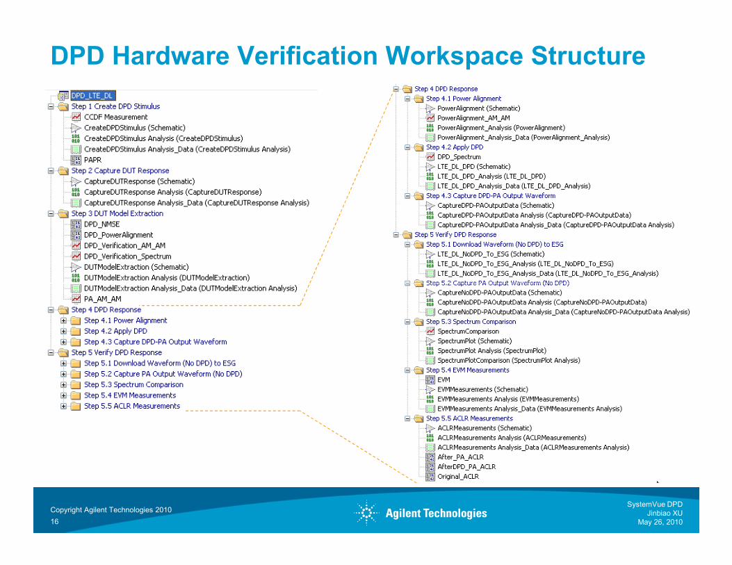
DPD Hardware Verification Workspace Structure
Copyright Agilent Technologies 2010SystemVue DPD
Jinbiao XU
May 26, 201016
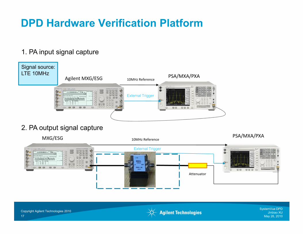
DPD Hardware Verification Platform
10MHz Reference
External Trigger
1. PA input signal capture
Signal source:
LTE 10MHzAgilent MXG/ESG PSA/MXA/PXA
10MHz Reference
External Trigger
Attenuator
2. PA output signal capturePSA/MXA/PXAMXG/ESG
Copyright Agilent Technologies 2010SystemVue DPD
Jinbiao XU
May 26, 201017
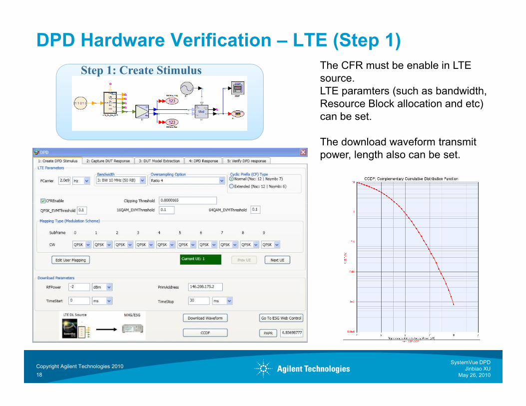
DPD Hardware Verification – LTE (Step 1)
Step 1: Create Stimulus The CFR must be enable in LTE
source.
LTE paramters (such as bandwidth,
Resource Block allocation and etc)
can be set.
The download waveform transmit
power, length also can be set.
Copyright Agilent Technologies 2010SystemVue DPD
Jinbiao XU
May 26, 201018
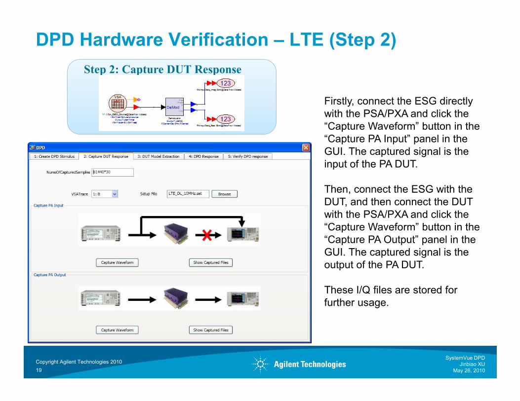
Step 2: Capture DUT Response
DPD Hardware Verification – LTE (Step 2)
Firstly, connect the ESG directly
with the PSA/PXA and click the
“Capture Waveform” button in the
“Capture PA Input” panel in the
GUI. The captured signal is the
input of the PA DUT.
Then, connect the ESG with the
DUT, and then connect the DUT DUT, and then connect the DUT
with the PSA/PXA and click the
“Capture Waveform” button in the
“Capture PA Output” panel in the
GUI. The captured signal is the
output of the PA DUT.
These I/Q files are stored for
further usage.
Copyright Agilent Technologies 2010SystemVue DPD
Jinbiao XU
May 26, 201019
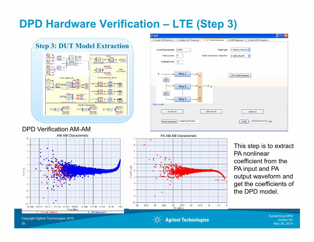
Step 3: DUT Model Extraction
DPD Hardware Verification – LTE (Step 3)
This step is to extract
PA nonlinear
coefficient from the
PA input and PA
output waveform and
get the coefficients of
the DPD model.
DPD Verification AM-AM
Copyright Agilent Technologies 2010SystemVue DPD
Jinbiao XU
May 26, 201020
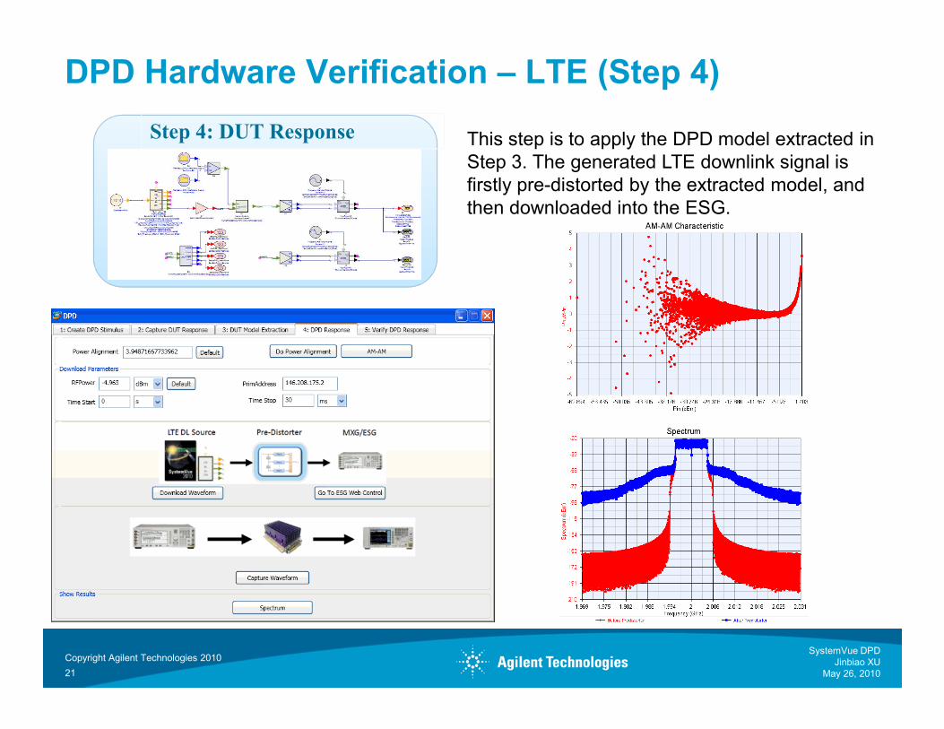
DPD Hardware Verification – LTE (Step 4)
Step 4: DUT Response This step is to apply the DPD model extracted in
Step 3. The generated LTE downlink signal is
firstly pre-distorted by the extracted model, and
then downloaded into the ESG.
Copyright Agilent Technologies 2010SystemVue DPD
Jinbiao XU
May 26, 201021
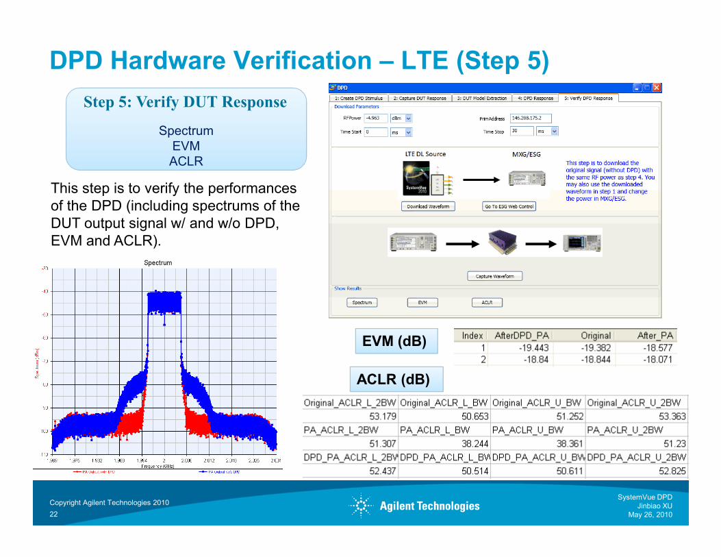
DPD Hardware Verification – LTE (Step 5)
Spectrum
EVM
ACLR
Step 5: Verify DUT Response
This step is to verify the performances
of the DPD (including spectrums of the
DUT output signal w/ and w/o DPD,
EVM and ACLR).
EVM (dB)
ACLR (dB)
Copyright Agilent Technologies 2010SystemVue DPD
Jinbiao XU
May 26, 201022
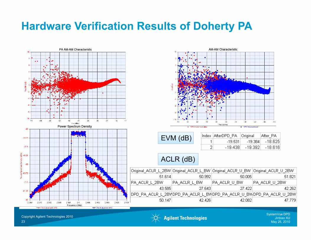
Hardware Verification Results of Doherty PA
EVM (dB)
ACLR (dB)
Copyright Agilent Technologies 2010SystemVue DPD
Jinbiao XU
May 26, 201023

1. Lei Ding, Zhou G.T., Morgan D.R., Zhengxiang Ma, Kenney J.S., Jaehyeong Kim, Giardina C.R., “A robust digital
baseband predistorter constructed using memory polynomials”, Communications, IEEE Transactions on, Jan. 2004,
Volume: 52, Issue:1, page 159-165.
2. Lei Ding, “Digital Predistortion of Power Amplifiers for Wireless Applications”, PhD Thesis, March 2004.
3. Roland Sperlich, “Adaptive Power Amplifier Linearization by Digital Pre-Distortion with Narrowband Feedback using
Genetic Algorithms”, PhD Thesis, 2005.
4. Helaoui, M. Boumaiza, S. Ghazel, A. Ghannouchi, F.M., “Power and efficiency enhancement of 3G multicarrier
amplifiers using digital signal processing with experimental validation”, Microwave Theory and Techniques, IEEE
Transactions on, June 2006, Volume: 54, Issue: 4, Part 1, page 1396-1404.
5. H. A.Suraweera, K. R. Panta, M. Feramez and J. Armstrong, “OFDM peak-to-average power reduction scheme with
spectral masking,” Proc. Symp. on Communication Systems, Networks and Digital Signal Processing, pp.164-167, July
2004.
References
2004.
6. Zhao, Chunming; Baxley, Robert J.; Zhou, G. Tong; Boppana, Deepak; Kenney, J. Stevenson, “Constrained Clipping for
Crest Factor Reduction in Multiple-user OFDM”, Radio and Wireless Symposium, 2007 IEEE Volume , Issue , 9-11 Jan.
2007 Page(s):341- 344.
7. Olli Vaananen, “Digital Modulators with Crest Factor Reduction Techniques”, PhD Thesis, 2006
8. Boumaiza, et a, “On the RF/DSP Design for Efficiency of OFDM Transmitters” , IEEE Transactions on
Microwave Theory and Techniques, Vol. 53, No. 7, July 2005, pp 2355-2361.
9. Boumaiza, Slim, “Advanced Memory Polynomial Linearization Techniques,” IMS2009 Workshop WMC
(Boston, MA), June 2009.
10. Amplifier Pre-Distortion Linearization and Modeling Using X-Parameters, Agilent EEsof EDA
Copyright Agilent Technologies 2010
24
SystemVue DPD
Jinbiao XU
May 26, 2010