Embed Size (px)
Citation preview

1FEATURES
APPLICATIONS
DESCRIPTION
bq78PL114
www.ti.com ................................................................................................................................................ SLUS850B–SEPTEMBER 2008–REVISED APRIL 2009
PowerLAN™ Master Gateway Battery Management ControllerWith PowerPump™ Cell Balancing Technology
– bq78PL114S12: < 300 µA Active, < 185 µAStandby, < 85 µA Ship, and < 1 µA
23• bq78PL114 Designed for Managing 3- toUndervoltage Shutdown8-Series-Cell Battery Systems
• Accurate, Advanced Temperature Monitoring• bq78PL114S12 Firmware Upgrade Supports 3-of Cells and MOSFETs With up to 12 Sensorsto 12-Series-Cell Battery Systems
• Fail-Safe Operation of Pack Protection– Adds Support for LCD and Electronic PaperCircuits: Up to Three Power MOSFETs andDisplays or EPDsOne Secondary Safety Output (Fuse)– Configurable for 11-A, 26-A, or 110-A
• Fully Programmable Voltage, Current, Balance,Operating Currentsand Temperature-Protection Features• Systems With More Than Four Series Cells
• External Inputs for Auxiliary MOSFET ControlRequire External bq76PL102 Dual-CellMonitors • Smart Battery System 1.1 Compliant via
SMBus• SmartSafety Features:– Prevention: Optimal Cell Management– Diagnosis: Improved Sensing of Cell • Portable Medical Instruments and TestProblems Equipment– Fail Safe: Detection of Event Precursors • Mobility Devices (E-Bike)
• Rate-of-Change Detection of All Important Cell • Uninterruptible Power Supplies and Hand-HeldCharacteristics: Tools– Voltage– Impedance– Cell Temperature The bq78PL114 master gateway battery controller is
part of a complete Li-Ion control, monitoring, and• PowerPump Technology Transfers Chargesafety solution designed for large series cell strings.Efficiently From Cell to Cell During All
Operating Conditions, Resulting in Longer The bq78PL114 and bq78PL114S12 along withbq76PL102 PowerLAN™ dual-cell monitors provideRun Time and Cell Lifecomplete battery-system control, communications,– bq78PL114S12 Adds User-Configurableand safety functions for a structure of three up toPowerPump Cell-Balancing Modes twelve series cells. This PowerLAN system provides
• High-Resolution 18-Bit Integrating Delta-Sigma simultaneous, synchronized voltage and currentCoulomb Counter for Precise Charge-Flow measurements using one A/D per-cell technology.Measurements and Gas Gauging This eliminates system-induced noise from
measurements and allows the precise, continuous,• Multiple Independent Δ-Σ ADCs: One-per-Cellreal-time calculation of cell impedance under allVoltage, Plus Separate Temperature, Current,operating conditions, even during widely fluctuatingand Safety load conditions.
• Simultaneous, Synchronous Measurement ofPowerPump technology transfers charge betweenPack Current and Individual Cell Voltagescells to balance their voltage and capacity. Balancing• Very Low Power Consumption is possible during all battery modes: charge,
– bq78PL114: < 250 µA Active, < 150 µA discharge, and rest. Highly efficient charge-transferStandby, < 40 µA Ship, and < 1 µA circuitry nearly eliminates energy loss while providing
true real-time balance between cells, resulting inUndervoltage Shutdownlonger run-time and improved cycle life.
1
Please be aware that an important notice concerning availability, standard warranty, and use in critical applications of TexasInstruments semiconductor products and disclaimers thereto appears at the end of this data sheet.
2PowerLAN, PowerPump, bqWizard are trademarks of Texas Instruments.3All other trademarks are the property of their respective owners.
PRODUCTION DATA information is current as of publication date. Copyright © 2008–2009, Texas Instruments IncorporatedProducts conform to specifications per the terms of the TexasInstruments standard warranty. Production processing does notnecessarily include testing of all parameters.

DESCRIPTION (CONTINUED)
bq78PL114
SLUS850B–SEPTEMBER 2008–REVISED APRIL 2009................................................................................................................................................ www.ti.com
These devices have limited built-in ESD protection. The leads should be shorted together or the device placed in conductive foamduring storage or handling to prevent electrostatic damage to the MOS gates.
Temperature is sensed by up to 12 external sensors and one on-chip sensor. This permits accurate temperaturemonitoring of each cell individually. Firmware is then able to compensate for the temperature-induced effects oncapacity, impedance, and OCV on a cell-by-cell basis, resulting in superior charge/ discharge and balancingcontrol.
External MOSFET control inputs provide user- definable direct hardware control over MOSFET states. Smartcontrol prevents excessive current through MOSFET body diodes. Auxiliary inputs can be used for enhancedsafety and control in large multicell arrays.
The bq78PL114 is completely user-configurable, with parametric tables in flash memory to suit a variety of cellchemistries, operating conditions, safety controls, and data reporting needs. It is easily configured using thesupplied bqWizard™ graphical user interface (GUI). The device is fully programmed and requires no algorithm orfirmware development.
The bq78PL114 can be upgraded to the bq78PL114S12 by downloading the bq78PL114S12 firmware. Thefirmware can be downloaded using the bqWizard application or during manufacturing. Upgrading to thebq78Pl114S12 changes the functionality of the LED1–LED5, LEDEN, and N/C pin #29. The bq78PL114S12 pinfunctions of LED1/SEG1–LED5/SEG5, PSH/BP/TP, and FIELD support LED, LCD, and electronic paper displays(EPDs). The user can configure the bq78PL114S12 for the desired display type.
In this document all descriptions for the bq78PL114 apply to the bq78PL114S12 except where differentbq78PL114S12 functionality is specifically described.
2 Submit Documentation Feedback Copyright © 2008–2009, Texas Instruments Incorporated
Product Folder Link(s): bq78PL114
FLA
SH
PRE
CHG
EFCID
EFCIC
SMBus
DSG
SMBCLK
SMBDAT
SPROT
CSBAT
CSPACK
GPIO6
CE
LL
4Voltage
Temp
Balance
V4
P4N
P4S
XT4
V3
P3N
P3S
XT3
V2
P2N
P2S
XT2
CE
LL
3Voltage
Temp
BalanceC
ELL
2Voltage
Temp
Balance
CE
LL
1Voltage
Temp
Balance
2.5 V LDOVLDO1 Watchdog
Coulomb Counter CCBAT
CCPACKCurrent A/D
Core / CPU
Measure
I/O
Safety
SR
AM
RSTN
InternalTemperature
RISC
CPU
InternalOscillator
ResetLogic
First-Level Safetyand
FET Control
Second-LevelSafety
LED1–5,LEDEN
B0320-02
PowerLANCommunication
Link
P-LAN
V1
P1N
P1S
XT1
bq78PL114
www.ti.com ................................................................................................................................................ SLUS850B–SEPTEMBER 2008–REVISED APRIL 2009
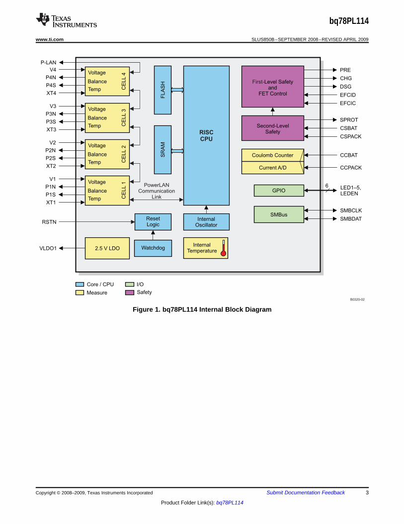
Figure 1. bq78PL114 Internal Block Diagram
Copyright © 2008–2009, Texas Instruments Incorporated Submit Documentation Feedback 3
Product Folder Link(s): bq78PL114

Core / CPU
Measure
I/O
Safety
B0320-03
FLA
SH
PRE
CHG
EFCID
EFCIC
SMBus
DSG
SMBCLK
SMBDAT
SPROT
CSBAT
CSPACK
GPIO7
CE
LL
4Voltage
Temp
Balance
V4
P4N
P4S
XT4
V3
P3N
P3S
XT3
V2
P2N
P2S
XT2
CE
LL
3Voltage
Temp
BalanceC
ELL
2Voltage
Temp
Balance
CE
LL
1Voltage
Temp
Balance
2.5 V LDOVLDO1 Watchdog
Coulomb Counter CCBAT
CCPACKCurrent A/D
SR
AM
RSTN
InternalTemperature
RISC
CPU
InternalOscillator
ResetLogic
First-Level Safetyand
FET Control
Second-LevelSafety
LED1–5/SEG1–5,PSH/BP/TP,FIELD
PowerLANCommunication
Link
P-LAN
V1
P1N
P1S
XT1
bq78PL114
SLUS850B–SEPTEMBER 2008–REVISED APRIL 2009................................................................................................................................................ www.ti.com
Figure 2. bq78PL114S12 Internal Block Diagram
4 Submit Documentation Feedback Copyright © 2008–2009, Texas Instruments Incorporated
Product Folder Link(s): bq78PL114

bq76PL102 CellMonitor WithPowerPumpBalancing
Pow
erL
AN
Com
munic
ation
Lin
k
PowerLANMaster GatewayBattery Controller
bq78PL114
PackPositive
PackNegative
Example 8-cell configuration shown
– +
SM
Bus
RS
EN
SE
Pack P
rote
ction
Circuits a
nd F
use
B0332-01
bq76PL102 CellMonitor WithPowerPumpBalancing
bq78PL114
www.ti.com ................................................................................................................................................ SLUS850B–SEPTEMBER 2008–REVISED APRIL 2009
Figure 3. Example bq78PL114 PowerLAN Multicell System Implementation (8 Cells)
Copyright © 2008–2009, Texas Instruments Incorporated Submit Documentation Feedback 5
Product Folder Link(s): bq78PL114

PowerLANCommunication
Link
Po
we
rLA
NM
aste
r G
ate
wa
y B
att
ery
Co
ntr
olle
rb
q7
8P
L11
4S
12
Pa
ck
Po
sitiv
e
Pa
ck
Ne
ga
tive
Exa
mp
le 1
2-c
ell
co
nfig
ura
tio
n s
ho
wn
SMBus
RSENSE
Pack ProtectionCircuits and Fuse
B0
33
2-0
2
bq
76
PL
10
2D
ua
l-C
ell
Mo
nito
rb
q7
6P
L1
02
Du
al-C
ell
Mo
nito
rB
q7
6P
L1
02
Du
al-C
ell
Mo
nito
rB
q7
6P
L1
02
Du
al-C
ell
Mo
nito
r
V1
X1
TV
2X
2T
V3
X3
TV
4X
4T
V1
T1
V2
T2
V1
T1
V2
T2
V1
T1
V2
T2
V1
T1
V2
T2
1
2
3
4
5
6
7
8
9
10
11
12
bq78PL114
SLUS850B–SEPTEMBER 2008–REVISED APRIL 2009................................................................................................................................................ www.ti.com
Figure 4. Example bq78PL114S12 System Implementation (12 Cells)
6 Submit Documentation Feedback Copyright © 2008–2009, Texas Instruments Incorporated
Product Folder Link(s): bq78PL114
AVAILABLE OPTIONS
P0023-16
bq78PL114RGZ Package
(Top View)
CHG
SD
O0
DSG
SD
I1
PRE
P1N
EFCIC
P2S
EFCID
P2N
CCBAT
SD
O2
CCPACK
SD
I3
VLDO1
P3
S
CSBAT
P3
N
CSPACK
P4
S
OSCI
P4
N
OSCO
P-L
AN
1
2
3
4
5
6
7
8
9
10
11
12
13
14
15
16
17
18
19
20
21
22
23
24
LED5
VS
S
LED4
V1
LED3
XT
1
LED2
XT
2
LED1
V2
LEDEN
VLD
O2
SPROT
V3
NC
XT
3
NC
XT
4
NC
V4
NC
SM
BD
AT
RSTN
SM
BC
LK
36
35
34
33
32
31
30
29
28
27
26
25
48
47
46
45
44
43
42
41
40
39
38
37
Thermal Pad
bq78PL114
www.ti.com ................................................................................................................................................ SLUS850B–SEPTEMBER 2008–REVISED APRIL 2009
ORDERING INFORMATIONPackage Temperature Quantity,Product Cell Configuration (1) Package Ordering NumberDesignator Range Transport Media
bq78PL114RGZT 250, tape and reelQFN-48, 7-mmbq78PL114 3 to 8 series cells RGZ –40°C to 85°C× 7-mm bq78PL114RGZR 2500, tape and reelbq78PL114S Firmware download3 to 12 series cells N/A N/A N/A N/A12 and upgrade
(1) For configurations consisting of more than four series cells, additional bq76PL102 parts must be used.
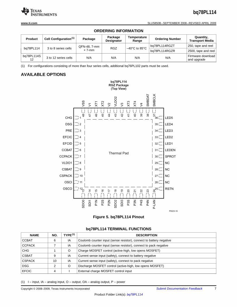
Figure 5. bq78PL114 Pinout
bq78PL114 TERMINAL FUNCTIONSNAME NO. TYPE (1) DESCRIPTION
CCBAT 6 IA Coulomb counter input (sense resistor), connect to battery negativeCCPACK 7 IA Coulomb counter input (sense resistor), connect to pack negativeCHG 1 O Charge MOSFET control (active-high, low opens MOSFET)CSBAT 9 IA Current sense input (safety), connect to battery negativeCSPACK 10 IA Current sense input (safety), connect to pack negativeDSG 2 O Discharge MOSFET control (active-high, low opens MOSFET)EFCIC 4 I External charge MOSFET control input
(1) I – input, IA – analog input, O – output, OA – analog output, P – power
Copyright © 2008–2009, Texas Instruments Incorporated Submit Documentation Feedback 7
Product Folder Link(s): bq78PL114

bq78PL114
SLUS850B–SEPTEMBER 2008–REVISED APRIL 2009................................................................................................................................................ www.ti.com
bq78PL114 TERMINAL FUNCTIONS (continued)NAME NO. TYPE (1) DESCRIPTION
EFCID 5 I External discharge MOSFET control inputLED1 32 O LED1 – open-drain, active-lowLED2 33 O LED2 – open-drain, active-lowLED3 34 O LED3 – open-drain, active-lowLED4 35 O LED4 – open-drain, active-lowLED5 36 O LED5 – open-drain, active-lowLEDEN 31 IO LEDEN – common-anode drive (active-low) and pushbutton inputNC 26 IO Connect 1-MΩ resistor to VSSNC 27 I Connect 1-MΩ resistor to VSSNC 28, 29 O No connectOSCI 11 I External oscillator input (no connect, internal oscillator used)OSCO 12 O External oscillator output (no connect, internal oscillator used)P1N 15 O Charge-balance gate drive, cell 1 northP2S 16 O Charge-balance gate drive, cell 2 southP2N 17 O Charge-balance gate drive, cell 2 northP3N 21 O Charge-balance gate drive, cell 3 northP3S 20 O Charge-balance gate drive, cell 3 southP4N 23 O Charge-balance gate drive, cell 4 northP4S 22 O Charge-balance gate drive, cell 4 southP-LAN 24 IO PowerLAN I/O to external bq76PL102 nodesPRE 3 O Precharge MOSFET control (active-high)RSTN 25 I Device reset, active-lowSDI1 14 I Connect to SDO0 via a capacitorSDI3 19 I Internal PowerLAN connection – connect to SDO2 through a 0.01-µF capacitorSDO0 13 O Requires 100-kΩ pullup resistor to VLDO1SDO2 18 O Internal PowerLAN connection – connect to SDI3 through a 0.01-µF capacitorSMBCLK 37 IO SMBus clock signalSMBDAT 38 IO SMBus data signalSPROT 30 O Secondary protection output, active-high (FUSE)V1 47 IA Cell-1 positive inputV2 44 IA Cell-2 positive inputV3 42 IA Cell-3 positive inputV4 39 IA Cell-4 positive inputVLDO1 8 P Internal LDO-1 output, bypass with 10-µF capacitor to VSSVLDO2 43 P Internal LDO-2 output, bypass with 10-µF capacitor to V2VSS 48 IA Cell-1 negative inputXT1 46 IA External temperature-sensor-1 inputXT2 45 IA External temperature-sensor-2 inputXT3 41 IA External temperature-sensor-3 inputXT4 40 IA External temperature-sensor-4 input– – P Thermal pad. Connect to VSS
8 Submit Documentation Feedback Copyright © 2008–2009, Texas Instruments Incorporated
Product Folder Link(s): bq78PL114
P0023-20
bq78PL114S12RGZ Package
(Top View)
CHG
SD
O0
DSG
SD
I1
PRE
P1N
EFCIC
P2S
EFCID
P2N
CCBAT
SD
O2
CCPACK
SD
I3
VLDO1
P3S
CSBAT
P3
N
CSPACK
P4S
OSCI
P4
N
OSCO
P-L
AN
1
2
3
4
5
6
7
8
9
10
11
12
13
14
15
16
17
18
19
20
21
22
23
24
LED5/SEG5
VS
S
LED4/SEG4
V1
LED3/SEG3
XT
1
LED2/SEG2
XT
2
LED1/SEG1
V2
PSH/BP/TP
VLD
O2
SPROT
V3
FIELD
XT
3
NC
XT
4
NC
V4
NC
SM
BD
AT
RSTN
SM
BC
LK
36
35
34
33
32
31
30
29
28
27
26
25
48
47
46
45
44
43
42
41
40
39
38
37
Thermal Pad
bq78PL114
www.ti.com ................................................................................................................................................ SLUS850B–SEPTEMBER 2008–REVISED APRIL 2009
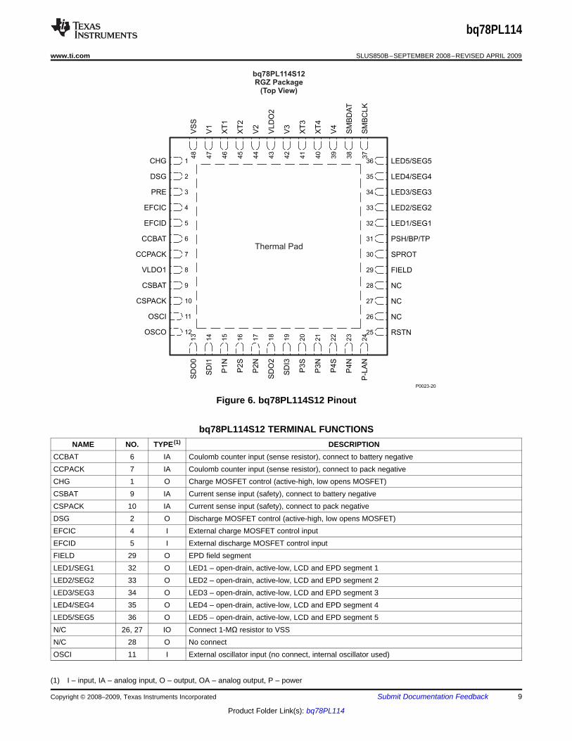
Figure 6. bq78PL114S12 Pinout
bq78PL114S12 TERMINAL FUNCTIONSNAME NO. TYPE (1) DESCRIPTION
CCBAT 6 IA Coulomb counter input (sense resistor), connect to battery negativeCCPACK 7 IA Coulomb counter input (sense resistor), connect to pack negativeCHG 1 O Charge MOSFET control (active-high, low opens MOSFET)CSBAT 9 IA Current sense input (safety), connect to battery negativeCSPACK 10 IA Current sense input (safety), connect to pack negativeDSG 2 O Discharge MOSFET control (active-high, low opens MOSFET)EFCIC 4 I External charge MOSFET control inputEFCID 5 I External discharge MOSFET control inputFIELD 29 O EPD field segmentLED1/SEG1 32 O LED1 – open-drain, active-low, LCD and EPD segment 1LED2/SEG2 33 O LED2 – open-drain, active-low, LCD and EPD segment 2LED3/SEG3 34 O LED3 – open-drain, active-low, LCD and EPD segment 3LED4/SEG4 35 O LED4 – open-drain, active-low, LCD and EPD segment 4LED5/SEG5 36 O LED5 – open-drain, active-low, LCD and EPD segment 5N/C 26, 27 IO Connect 1-MΩ resistor to VSSN/C 28 O No connectOSCI 11 I External oscillator input (no connect, internal oscillator used)
(1) I – input, IA – analog input, O – output, OA – analog output, P – power
Copyright © 2008–2009, Texas Instruments Incorporated Submit Documentation Feedback 9
Product Folder Link(s): bq78PL114

bq78PL114
SLUS850B–SEPTEMBER 2008–REVISED APRIL 2009................................................................................................................................................ www.ti.com
bq78PL114S12 TERMINAL FUNCTIONS (continued)NAME NO. TYPE (1) DESCRIPTION
OSCO 12 O External oscillator output (no connect, internal oscillator used)P1N 15 O Charge-balance gate drive, cell 1 northP2N 17 O Charge-balance gate drive, cell 2 northP2S 16 O Charge-balance gate drive, cell 2 southP3N 21 O Charge-balance gate drive, cell 3 northP3S 20 O Charge-balance gate drive, cell 3 southP4N 23 O Charge-balance gate drive, cell 4 northP4S 22 O Charge-balance gate drive, cell 4 southP-LAN 24 IO PowerLAN I/O to external bq76PL102 nodesPRE 3 O Precharge MOSFET control (active-high)PSH/BP/TP 31 IO Pushbutton detect for LED display, LCD backplane, EPD top plane and charge pumpRSTN 25 I Device reset, active-lowSDI1 14 I Connect to SDO0 via a capacitorSDI3 19 I Internal PowerLAN connection – connect to SDO2 through a 0.01-µF capacitorSDO0 13 O Requires 100-kΩ pullup resistor to VLDO1SDO2 18 O Internal PowerLAN connection – connect to SDI3 through a 0.01-µF capacitorSMBCLK 37 IO SMBus clock signalSMBDAT 38 IO SMBus data signalSPROT 30 O Secondary protection output, active-high (FUSE)V1 47 IA Cell-1 positive inputV2 44 IA Cell-2 positive inputV3 42 IA Cell-3 positive inputV4 39 IA Cell-4 positive inputVLDO1 8 P Internal LDO-1 output, bypass with 10-µF capacitor to VSSVLDO2 43 P Internal LDO-2 output, bypass with 10-µF capacitor to V2VSS 48 IA Cell-1 negative inputXT1 46 IA External temperature-sensor-1 inputXT2 45 IA External temperature-sensor-2 inputXT3 41 IA External temperature-sensor-3 inputXT4 40 IA External temperature-sensor-4 input– – P Thermal pad. Connect to VSS
10 Submit Documentation Feedback Copyright © 2008–2009, Texas Instruments Incorporated
Product Folder Link(s): bq78PL114

ABSOLUTE MAXIMUM RATINGS (1)
RECOMMENDED OPERATING CONDITIONS
bq78PL114
www.ti.com ................................................................................................................................................ SLUS850B–SEPTEMBER 2008–REVISED APRIL 2009
over operating free-air temperature range (unless otherwise noted)
RANGE UNITSTA Operating free-air temperature (ambient) –40 to 85 °CTstg Storage temperature –65 to 150 °CV4–V3 Maximum cell voltage –0.5 to 5.0 VV3–V2 Maximum cell voltage –0.5 to 5.0 VV2–V1 Maximum cell voltage –0.5 to 5.0 VV1–VSS Maximum cell voltage –0.5 to 5.0 VVoltage on LEDEN, SPROT, CCBAT,CCPACK, CSBAT, CSPACK, XT1, XT2, Maximum voltage on any I/O pin with respect to VSS –0.5 to (VLDO1 + 0.5) VOSCI, OSCO, P-LANVoltage on PSH/BP/TP (bq78PL114S12) Maximum voltage range with respect to VSS –0.5 to (VLDO1 + 0.5) VVoltage on LED1–LED5 Maximum voltage on I/O pin with respect to VSS –0.5 to 5.5 VVoltage on LED1/SEG1–LED5/SEG5 Maximum voltage on I/O pin –0.5 to 5.5 V(bq78PL114S12)
(V2 – 0.5) toVoltage on XT3, XT4 Maximum voltage range with respect to V2 V(VLDO2 + 0.5)EFCIC, EFCID Maximum voltage range with respect to VSS –0.5 to 5.5 VVoltage on SMBCLK, SMBDAT Maximum voltage range with respect to VSS –0.5 to 6 VVoltage on PRE, CHG, DSG Maximum voltage range with respect to VSS –0.5 to (VLDO1 + 0.5) VCurrent through PRE, CHG, DSG, Maximum current source/sink 20 mALED1–LED5, P-LANCurrent throughLED1/SEG1–LED5/SEG5, Maximum current source/sink 20 mA(bq78PL114S12, LED mode)VLDO1 maximum current Maximum current draw from VLDO 20 mA
JEDEC, JESD22-A114 human-body model, R = 1500 Ω, C =ESD tolerance 2 kV100 pFLead temperature, soldering Total time < 3 seconds 300 °C
(1) Stresses beyond those listed under Absolute Maximum Ratings may cause permanent damage to the device. These are stress ratingsonly, and functional operation of the device at these or any other conditions beyond those indicated under Recommended OperatingConditions is not implied. Exposure to absolute-maximum-rated conditions for extended periods may affect device reliability.
over operating free-air temperature range (unless otherwise noted)
MIN NOM MAX UNITVSUP Supply voltage—V1, V2, V3, V4 2.3 4.5 VVStartup Minimum startup voltage—V1, V2 2.9 VVIN Input cell voltage range—V(n+1) – V(n), n = 1, 2, 3, 4 0 4.5 VCVLDO1 VLDO 1 capacitor—VLDO1 2.2 10 47 µFCVLDO2 VLDO 2 capacitor—VLDO2 2.2 10 47 µFCVn Cell-voltage capacitor—Vn 1 µF
Copyright © 2008–2009, Texas Instruments Incorporated Submit Documentation Feedback 11
Product Folder Link(s): bq78PL114

ELECTRICAL CHARACTERISTICS
DC Characteristics
Voltage-Measurement Characteristics
bq78PL114
SLUS850B–SEPTEMBER 2008–REVISED APRIL 2009................................................................................................................................................ www.ti.com
TA = –40°C to 85°C (unless otherwise noted)
PARAMETER TEST CONDITIONS MIN TYP MAX UNITVCELL
(1) Operating range Cells balanced 2.3 4.5 VIDD Operating-mode current Measure / report state, bq78PLL114 250 µA
Measure / report state, bq78PLL114S12 300ISTBY Standby-mode current SMBCLK = SMBDAT = L, bq78PLL114 100 µA
SMBCLK = SMBDAT = L, 185bq78PLL114S12
ISHIP Ship-mode current bq78PLL114 30 µAbq78PLL114S12 85
Extreme cell under voltage All cells < 2.7 V and any cell < ECUV setIECUV 1 µAshutdown current pointVOL SPROT, LEDEN, IOL < 4 mA 0 0.5 V
PSH/BP/TP(bq78PL114S12),FIELD(bq78PL114S12)
VOH(2) SPROT, LEDEN, IOH < –4 mA VLDO1 – 0.1 V
PSH/BP/TP(bq78PL114S12),FIELD(bq78PL114S12)
VIL SPROT, LEDEN, 0.25 VLDO1 VPSH/BP/TP(bq78PL114S12),FIELD(bq78PL114S12)
VIH SPROT, LEDEN, 0.75 VLDO1 VPSH/BP/TP(bq78PL114S12),FIELD(bq78PL114S12)
(1) Device should be configured to enter shutdown state when cell voltages are below 2.5 V.(2) Does not apply to SMBus pins.
over operating free-air temperature range (unless otherwise noted)
PARAMETER TEST CONDITIONS MIN TYP MAX UNITMeasurement range 2.5 4.5 VResolution <1 mV
25°C ±5Accuracy mV
0°C to 60°C ±10
12 Submit Documentation Feedback Copyright © 2008–2009, Texas Instruments Incorporated
Product Folder Link(s): bq78PL114

Current-Sense Characteristics
Coulomb-Counter Characteristics (1) (2)
Current-Sense (Safety) Characteristics (1)
Internal Temperature-Sensor Characteristics (1)
bq78PL114
www.ti.com ................................................................................................................................................ SLUS850B–SEPTEMBER 2008–REVISED APRIL 2009
over operating free-air temperature range (unless otherwise noted)
PARAMETER TEST CONDITIONS MIN TYP MAX UNITMeasurement range (1) (bq78PL114) –0.2 0.2 VMeasurement range (2) (bq78PL114S12, 3-mΩ –0.077 0.077 Vsense resistor)Measurement range (2) (bq78PL114S12, 1-mΩ –0.1 0.1 Vand 10-mΩ sense resistors)Input offset TA = 25°C ±50 µVOffset drift TA = 0°C to 60°C 0.5 µV/°CResolution (bq78PL114) 18 µVResolution (bq78PL114S12, 3-mΩ sense 6.9 µVresistor)Resolution (bq78PL114S12, 1-mΩ and 10-mΩ 10 µVsense resistors)Full-scale error (3) TA = 25°C ±0.1%Full-scale error drift TA = 0°C to 60°C 50 PPM/°C
(1) Default range. Corresponds to ±10 A using a 5-mΩ sense resistor.(2) The bq78PL114S12 firmware upgrade supports three sense-resistor options, 10 mΩ, 3 mΩ, and 1 mΩ.(3) After calibration. Accuracy is dependent on system calibration and temperature coefficient of sense resistor.
over operating free-air temperature range (unless otherwise noted)
PARAMETER TEST CONDITIONS MIN TYP MAX UNITResolution 5 nVhIntergral nonlinearity 0.008%Snap-to-zero (deadband) ±100 (3) µV
(1) Shares common input with current-sense section(2) After calibration. accuracy is dependent on system calibration and temperature coefficient of sense resistor.(3) Corresponds to 20 mA using 5-mΩ sense resistor
over operating free-air temperature range (unless otherwise noted)
PARAMETER TEST CONDITIONS MIN TYP MAX UNITMeasurement range –0.312 0.312 V
Short-circuit detection 10Resolution mV
Overcurrent detection, charge and discharge 1.25
(1) Post calibration: Dependent on system calibration and temperature coefficient of sense resistor. Uncertainty is 1.5 LSB.
over operating free-air temperature range (unless otherwise noted)
PARAMETER TEST CONDITIONS MIN TYP MAX UNITMeasurement range –30 85 °CResolution 0.1 °CAccuracy (1) –30° to 85° ±1 °C
(1) After calibration
Copyright © 2008–2009, Texas Instruments Incorporated Submit Documentation Feedback 13
Product Folder Link(s): bq78PL114

LDO Voltage Characteristics (1)
External Temperature-Sensor(s) Typical Characteristics (1)
SMBus Characteristics (1)
bq78PL114
SLUS850B–SEPTEMBER 2008–REVISED APRIL 2009................................................................................................................................................ www.ti.com
over operating free-air temperature range (unless otherwise noted)
PARAMETER TEST CONDITIONS MIN TYP MAX UNITVLDO1 LDO1 operating voltage, referenced to TA = –40C to 85C, load = 200 µA 2.425 2.5 2.575 V
VSSVLDO2 LDO2 operating voltage, referenced to V2 TA = –40C to 85C, load = 2 mA 2.425 2.5 2.575 V
(1) After calibration
over operating free-air temperature range (unless otherwise noted)
PARAMETER TEST CONDITIONS MIN TYP MAX UNITMeasurement range (2) –40 90 °CResolution 0.2 °C
25° ±1Accuracy (3) °C
0° to 85° ±2
(1) Typical for dual-diode (MMBD4148 or equivalent) external sensor using recommended circuit(2) Range of diode sensors may exceed operational limits of IC and battery cells.(3) Typical behavior after calibration, final result dependent on specific component characteristics
over operating free-air temperature range (unless otherwise noted)
PARAMETER TEST CONDITIONS MIN TYP MAX UNITVIL Input low voltage 0 0.8 VVIH Input high voltage 2.1 5.5 VVOL Output low voltage 350-µA sink current 0 0.4 VCI Capacitance, each I/O pin 10 pFfSCL SCLK nominal clock frequency TA = 25°C 100 kHz
VBUS 5 V nominal 13.3 45.3RPU
(2) Pullup resistors for SCLK, SDATA kΩVBUS 3 V nominal 2.4 6.8
(1) SMBus timing and signals meet the SMBus 2.0 specification requirements under normal operating conditions. All signals are measuredwith respect to PACK-negative.
(2) Pullups are typically implemented external to the battery pack, and are selected to meet SMBus requirements.
14 Submit Documentation Feedback Copyright © 2008–2009, Texas Instruments Incorporated
Product Folder Link(s): bq78PL114

bq78PL114PowerLAN
Gateway BatteryManagement
Controller
RPRE
+ PACK+
–
SMBCLK
SMBDAT
RSENSE
PACK–
XT1–XT4
TemperatureSensor (typ.)
SPROT
LED1–LED5
Typical six-cell configuration shown.Additional cells added via PowerLAN connection.Some components omitted for clarity.
V2
V3
V4
V1
VLDO2
CRFI
VLDO1
RSTN
SDO2
SDI3
EFCID
EFCIC
One of 4 externalsensors shown
P-LAN
5
CELL 6
CELL 5
V2
V1
SDI1
SDO0
Level-Shift Circuits
CH
G
DS
G
PR
E
ES
D P
rote
ction
SM
Bus
Au
x F
ET
Co
ntr
ol
Th
erm
al P
ad
VS
S
CS
BA
T
CC
BA
T
CC
PA
CK
CS
PA
CK
Ce
ll B
ala
ncin
gC
ircu
its
Ce
ll B
ala
ncin
g C
ircu
its
bq
76
PL
102
CELL 4
CELL 3
CELL 2
CELL 1
S0342-02
bq78PL114
www.ti.com ................................................................................................................................................ SLUS850B–SEPTEMBER 2008–REVISED APRIL 2009
Figure 7. bq78PL114 Simplified Example Circuit Diagram
Copyright © 2008–2009, Texas Instruments Incorporated Submit Documentation Feedback 15
Product Folder Link(s): bq78PL114

FEATURE SET
Primary (First-Level) Safety Features
Secondary (Second-Level) Safety Features
Charge Control Features
Gas Gauging
Display Types
bq78PL114
SLUS850B–SEPTEMBER 2008–REVISED APRIL 2009................................................................................................................................................ www.ti.com
The bq78PL114 implements a breadth of system protection features which are easily configured by thecustomer. First-level protections work by controlling the MOSFET switches. These include:• Battery cell over/undervoltage protection• Pack over/undervoltage protection• Charge and discharge overcurrent protection• Short-circuit protection• External MOSFET control inputs (EFCIx) with programmable polarity• Up to 12 external temperature inputs for accurate cell and MOSFET monitoring• Watchdog timer protection• Brownout detection and protection against extreme pack undervoltage
The bq78PL114 can detect more serious system faults and activate the SPROT pin, which can be used to openan in-line chemical fuse to permanently disable the pack. Secondary optional features include• Fully independent of first-level protections• SmartSafety algorithms for early detection of potential faults
– Temperature abnormalities (variances, extremes, rate of change, etc.)– Disconnected cell voltage inputs– Cell imbalance exceeds safety limits– Impedance rise due to cell or weld strap fault
• MOSFET failure or loss of MOSFET control• Safety overvoltage, pack and cell• Safety overtemperature, limits for both charge and discharge• Safety overcurrent, charge and discharge• Failed current measurement, voltage measurement, or temperature measurement
• Meets SMBus 2.0 and Smart Battery System (SBS) Specification 1.1 requirements• Active cell balancing using patented PowerPump technology, which eliminates unrecoverable capacity loss
due to normal cell imbalance• Balancing-current monitoring to detect cell problems• Simultaneous, synchronous measurement of all cell voltages in a pack• Simultaneous, synchronous measurement of pack current with cell voltages• Reports target charging current and/or voltage to an SBS Smart Charger• Reports the chemical state-of-charge for each cell and pack• Supports precharging and zero-volt charging with separate MOSFET control• Programmable, Chemistry-specific parameters• Fault reporting
• The bq78PL114 accurately reports battery cell and pack state-of-charge (SOC). No full charge/dischargecycle is required for accurate reporting.
• State-of-charge is reported via SMBus and optional display.• 18-bit integrating delta-sigma ADC coulomb counter, with programmable snap-to-zero value
• The bq78PL114 drives a three- to five-segment LED display in response to a pushbutton (LEDEN) inputsignal. Each LED pin can sink up to 10 mA.
16 Submit Documentation Feedback Copyright © 2008–2009, Texas Instruments Incorporated
Product Folder Link(s): bq78PL114

Lifetime Logging (Readable via SMBus)
Forensic Data Logging (Readable via SMBus)
Power Modes
OPERATION
bq78PL114
www.ti.com ................................................................................................................................................ SLUS850B–SEPTEMBER 2008–REVISED APRIL 2009
• The bq78PL114S12 drives a three- to five-segment static liquid-crystal display.• The bq78PL114S12 drives a three- to five-segment electronic paper display. An external 15-V voltage source
is required. E Ink Corporation supplies this type of display.
The display type is selected via the parameter set.
• Recording of faults, events, anomalies, minimum and maximum values• Maximum/minimum temperature• Maximum/minimum pack voltage• Maximum/minimum cell voltage in a pack• Maximum charge and discharge currents
• Last known full capacity of each cell• Cycle count and/or cumulative number of ampere-hours delivered by the battery• Battery pack status: being charged, discharged, or at rest• Balancing effort required by each bank of cells to maintain balance• Last 10 failures causing first-level safety action• Forensic data up-loadable to host CPU via SMBus
• Normal Mode: The bq78PL114 performs measurements and calculations, makes decisions, and updatesinternal data approximately once per second. All safety circuitry is fully functional in this mode.
• Standby Mode: The bq78PL114 performs as in normal mode, but at a dramatically reduced rate to lowerpower consumption at times when the host computer is inactive or the battery system is not being used. Allsafety circuitry remains fully functional in this mode.
• Ship Mode: The bq78PL114 disables (opens) all the protection MOSFETs, and continues to monitortemperature and voltage, but at a reduced measurement rate to dramatically lower power consumption.Environmental data is saved in flash as a part of the historical record. Safety circuitry is disabled in this mode.The device does not enter this power state as a part of normal operation; it is intended for use after factoryprogramming and test. Entry occurs only after a unique SMBus command is issued. Exit occurs when theSMBus lines return to an active state.
• Extreme Cell Undervoltage (ECUV) Shutdown Mode: In this mode, the bq78PL114 draws minimal currentand the charge and discharge protection MOSFETs are disabled (opened). The precharge MOSFET remainsenabled when a charge voltage is present. Safety circuitry is disabled in this mode. The device does not enterthis mode as a part of normal operation; it enters this state during extreme cell undervoltage conditions(ECUV). The ECUV threshold is programmable between 2.3 V and 2.7 V, with 2.5 V being typical.
OVERCURRENTSTATE ENTRY CONDITION EXIT CONDITIONPROTECTIONNormal operation as determined by firmware Firmware directed to the following operatingActive Fully active modesNo load current flowing for predeterminedStandby Fully active Load activitytime
Ship Not active Protected SMBus command SMBus becomes activeExtreme cell Not active (precharge Vcell charge above ECUV recovery thresholdEnabled when Vcell < ECUVundervoltage enabled) (2.7 V/cell typical)
The bq78PL114 battery-management controller serves as a master controller for a Li-Ion battery systemconsisting of up to 8 cells in series. The bq78PL114S12 firmware upgrade supports up to 12 cells in series. Anynumber of cells may be connected in parallel; other system or safety issues limit the number of parallel cells. Thebq78PL114 provides extraordinarily precise state-of-charge gas gauging along with first- and second-level packsafety functions. Voltage and current measurements are performed synchronously and simultaneously for allcells in the system, allowing a level of precision not previously possible in battery management. Temperature is
Copyright © 2008–2009, Texas Instruments Incorporated Submit Documentation Feedback 17
Product Folder Link(s): bq78PL114

PowerLAN Communication Link
Safety
Cell Balancing
bq78PL114
SLUS850B–SEPTEMBER 2008–REVISED APRIL 2009................................................................................................................................................ www.ti.com
measured by up to four additional external temperature sensors. With the bq78PL114S12 firmware upgrade, upto eight more are available in remote bq76PL102 dual-cell battery monitors. Coulomb counting is capturedcontinuously by a dedicated 18-bit integrating delta-sigma ADC in the bq78PL114. The CPU in the bq78PL114 isalso responsible for system data calculations, black-box forensic data storage, and communicating parametersvia the SMBus interface. The bq78PL114S12 firmware can be downloaded to existing bq78PL114 parts usingthe bqWizard GUI or during the manufacturing checkout process.
PowerLAN technology is Texas Instruments’ patented serial network and protocol designed specifically forbattery management in a multicell system environment. The PowerLAN link is used to initiate and reportmeasurements of cell voltage and temperature, and control cell balancing. The bq78PL114 serves as the mastercontroller of the PowerLAN link and can interface to multiple bq76PL102 dual-cell battery monitors, whichmeasure and balance additional cells. The bq78PL114 monitors the first three or four cells, and bq76PL102s canbe added to monitor more series cells.
The PowerLAN link isolates voltages from adjacent bq76PL102 devices to permit high-voltage stack assemblywithout compromising precision and accuracy. The PowerLAN link is expandable to support up to 12 cells inseries. Each bq76PL102 handles voltage and temperature measurements, as well as balancing for two cells. ThePowerLAN link provides high ESD tolerance and high immunity to noise generated by nearby digital circuitry orswitching currents. Each bq76PL102 has both a PowerLAN input and PowerLAN output: Received data isbuffered and retransmitted, permitting high numbers of nodes without loss of signal fidelity. Signals arecapacitor-coupled between nodes, providing dc isolation.
Unique in the battery-management controller market, the bq78PL114 simultaneously measures voltage andcurrent using independent and highly accurate delta-sigma ADCs. This technique removes virtually all systemicnoise from measurements, which are made during all modes of battery operation: charge, discharge, and rest.The bq78PL114 also directs all connected bq76PL102 dual-cell battery monitors to measure each cell voltagesimultaneously with the bq78PL114 measurements. Battery impedance and self-discharge characteristics arethus measured with an unprecedented level of accuracy in real time. The bq78PL114 applies this preciseinformation to SmartSafety algorithms to detect certain anomalies and conditions which may be indicative ofinternal cell faults, before they become serious problems.
The bq78PL114 uses its enhanced measurement system to detect system faults including cell under- andovervoltage, cell under- and overtemperature, system overvoltage, and system overcurrent. First-level safetyalgorithms first attempt to open the MOSFET safety switches. If this fails, second-level safety algorithms activatethe SPROT output, normally used to open a fuse and provide permanent, hard protection for the systems.External MOSFET control inputs with programmable polarity can also be used to operate the safety MOSFETsunder control of user supplied circuitry. The bq78PL114 continuously monitors these inputs. If any MOSFET failsto open when commanded; the 2nd level safety algorithms also activate the SPROT output. All first- andsecond-level safety algorithms have fully programmable time delays to prevent false triggering.
Patented PowerPump cell balancing technology drastically increases the useful life of battery packs byeliminating the cycle life fade of multi-cell packs due to cell imbalance. PowerPump technology efficientlytransfers charge from cell to cell, rather than simply bleeding off charging energy as heat as is typically done withresistive-bleed balancing circuits. Balancing is configurable and may be performed during any battery operationalmodes: charge, discharge, or rest. Compared to resistive bleed balancing, virtually no energy is lost as heat. Theactual balance current is externally scalable and can range from 10 mA to 1 A (100 mA typical) depending oncomponent selection and system or cell requirements.
A variety of techniques, such as simple terminal voltage, terminal voltage corrected for impedance andtemperature effects, or state-of-charge balancing, is easily implemented by the bq78PL114. By tracking thebalancing required by individual cells, overall battery safety is enhanced, often allowing early detection of softshorts or other cell failures. Balancing is achieved between all cells within the pack as dynamically determined bythe bq78PL114.
18 Submit Documentation Feedback Copyright © 2008–2009, Texas Instruments Incorporated
Product Folder Link(s): bq78PL114

Outputs
bq78PL114
www.ti.com ................................................................................................................................................ SLUS850B–SEPTEMBER 2008–REVISED APRIL 2009
Charge ControlThe CHG and PRE outputs are ordinarily used to drive MOSFET transistors controlling charge to the cell stack.Charge or precharge mode is selected based on the present cell voltage compared to the user-definable cellprecharge, undervoltage, and temperature thresholds. When below these limits, the PRE signal is active and theCHG signal is inactive. This turns on the precharge MOSFET and is used to charge a depleted system through acurrent-limiting series resistor. When all cell voltages are above the limit and the temperature is above the chargetemperature minimum, then the CHG output also becomes active and enables the charge MOSFET to turn on,providing a high-current path between charger and battery cells.
The CHG and PRE MOSFET control outputs are both disabled (low) when any cell reaches the safety cutoff limitor temperature threshold. During active charging modes (and above cell voltage thresholds), the dischargeMOSFET is also enabled to avoid excessive heating of the body diode. Similarly, the charge MOSFET is activeduring discharge, provided current flow is in the correct direction and no safety violations are present.
The bq78PL114S12 firmware upgrade supports the following configurable cell-balancing features:• Super-pump mode. When enabled this allows 60%–70% pump availability when there are no active safety
events and current is not flowing. While in super-pump mode, temperature rate-of-rise features are notavailable.
• Option to disable cell balancing during discharge• Option to disable cell balancing during charge
The CHG and PRE outputs are intended to drive buffer transistors acting as inverting level shifters.
Discharge ControlThe DSG output operates similarly to control-system discharging. It is enabled (high) by default. If a cell voltagefalls below a programmable threshold, or excessive current or other safety related fault is sensed, the DSGoutput is disabled (low) to prevent damage to the cells.
All facets of safely charging and discharging the cell stack are controlled by user-definable parameters whichprovide precise control over MOSFET states. Both system and cell over- and undervoltage limits are provided, aswell as programmable hysteresis to prevent oscillation. Temperature and current thresholds are also provided,each with independent timers to prevent nuisance activations.
The DSG output is intended to drive a buffer transistor acting as an inverting level-shifter.
DisplayThe bq78PL114 shows state-of-charge indication on a five-LED display in a bar-graph format. LEDEN is adual-function pin. One function is to control current to the LED display array. It also serves as an input thatmonitors for closure of a state-of-charge indicator (SOCi) push-button switch.
The bq78PL114S12 shows state-of-charge indication on LED, static liquid crystal, and electronic paper displaysor EPDs in a bar-graph-type format. The parameter set allows selection of display type and configuration.PSH/BP/TP is a multifunction pin. In LED display mode, PSH serves as an input that monitors for closure of astate-of-charge indicator (SOCi) push-button switch. In LCD mode, this pin is used to drive the LCD backplane.In EPD mode, this pin drives the top plane common signal of the display.
For both the bq78PL114 and bq78PL114S12, in LED display mode the signals LED1/SEG1–LED5/SEG5 arecurrent-sinking outputs designed to drive low-current LEDs.
For the bq78PL114S12 firmware in LCD and EPD modes, the LED1/SEG1–LED5/SEG5 pins drive the activesegments through external buffer transistors. In EPD mode, the FIELD pin drives the display background field.
Electronic paper displays require an external power supply, typically 15 V, to power the display. In EPD, modethe bq78PL114S12 strobes the display outputs for a user- programmable period of milliseconds to drive anexternal voltage multiplier or charge pump to the required display supply voltage. The display segments are thenupdated in a manner that ensures the required 0-Vdc segment voltage offset is maintained and keeps theexternal power supply at its nominal voltage.
Copyright © 2008–2009, Texas Instruments Incorporated Submit Documentation Feedback 19
Product Folder Link(s): bq78PL114

Inputs
bq78PL114
SLUS850B–SEPTEMBER 2008–REVISED APRIL 2009................................................................................................................................................ www.ti.com
Current MeasurementCurrent is monitored by four separate ADCs. All use the same very low-value sense resistor, typically 10, 5, 3, or1 milliohms in series with the pack negative connection. CCBAT and CCPACK connections to the sense resistoruse an R/C filter for noise reduction. (CSBAT and CSPACK are direct connections used for secondary safety).The bq78PL114 requires a 5-milliohm sense resistor. The bq78PL114S12 can be configured to use 10-, 3-, or1-milliohm sense resistors. When configured to use a 1-milliohm sense resistor, the maximum available packcapacity increases to 655 Ah from 65 Ah.
A 14-bit delta-sigma ADC is used to measure current flow accurately in both directions. The measurements aretaken simultaneously and synchronously with all the cell voltage measurements, even those cells measured bybq76PL102 dual-cell battery monitors.
Coulomb CountingA dedicated coulomb counter is used to measure charge flow with 18-bit precision in both directions by acalibrated, integrating delta-sigma ADC. This allows the bq78PL114 to keep very accurate state-of-charge (SOC)information and battery statistics. A small deadband is applied to further reduce noise effects. The coulombcounter is unique in that it continues to accumulate (integrate) current flow in either direction even as the rest ofthe internal microcontroller is placed in a very low power state, further lowering power consumption withoutcompromising system accuracy.
Safety CurrentTwo additional ADCs are used to directly monitor for overcurrent or short-circuit current conditions, independentlyof the internal function. This provides a direct and rapid response to insure pack integrity and safe operation byopening the appropriate MOSFETs. These functions are implemented in hardware, and do not require firmwarefor functionality.
Voltage MeasurementVoltage measurement is performed by four independent delta-sigma ADCs which operate simultaneously andare triggered synchronously so that all voltages are read at precisely the same moment. The bq78PL114coordinates the attached bq76PL102 dual-cell battery monitors so they also perform their cell voltagemeasurements in sync with the bq78PL114 voltage and current measurements. Voltage measurements areconverted with better than 1 mV of resolution, providing superior accuracy. One-ADC-per-cell technology meansthat voltage is also measured simultaneously with current, permitting accurate, real-time cell impedancecalculation during all operating conditions. This technique also provides greatly enhanced noise immunity andfiltering of the input signal without signal loss.
Temperature MeasurementXT1–XT4 are dedicated temperature-sensor inputs. Each external sensor consists of a low-cost silicon diode(dual diode in one package is recommended) and capacitor combination. Temperatures for cells 5 and above aremeasured by up to four external bq76PL102(s), and the temperature data is received by the bq78PL114 orbq78PL114S12 over the PowerLAN link for processing. The bq78PL114 or bq78PL114S12 can report all ofthese temperatures individually. The bq78PL114 allows multiplexed configuration of up to twelve temperaturesensors. This permits the pack designer to measure temperatures of all cells and other items such as the chargeand discharge MOSFETs. The bq78PL114S12 firmware uses the internal temperature sensor of the device forboard temperature measurements.
EFCIxThe external MOSFET control inputs are for user control of MOSFETs based on external circuitry and conditions.The polarity of the input signal is user-programmable. These pins can be used to force the protection MOSFETsto an OFF state.
20 Submit Documentation Feedback Copyright © 2008–2009, Texas Instruments Incorporated
Product Folder Link(s): bq78PL114

COMMUNICATIONS
SMBus
Smart Battery Data (SBData)
bq78PL114
www.ti.com ................................................................................................................................................ SLUS850B–SEPTEMBER 2008–REVISED APRIL 2009
The bq78PL114 uses the industry-standard Smart Battery System’s two-wire System Management Bus (SMBus)communications protocol for all external communication. SMBus version 2.0 is supported by the bq78PL114, andincludes clock stretching, bus fault time-out detection, and optional packet error checking (PEC). For additionalinformation, see the www.smbus.org and www.sbs-forum.org Web sites.
The data content and formatting of the bq78PL114 information conforms to the Smart Battery System’s (SBS)Smart Battery Data specification, version 1.1. See the SBS/SMBus site at www.sbs-forum.com for furtherinformation regarding these specifications.
This SBS Data (SBData) specification defines read/write commands for accessing data commonly required inlaptop computer applications. The commands are generic enough to be useful in most applications.
Because the bq78PL114 provides a wealth of control and battery information beyond the SBData standard, newcommand codes have been defined by Texas Instruments. In addition, new battery data features, such asstate-of-health, use newly defined extended SBData command codes. Standard SMBus protocols are used,although additional data values beyond those defined by the Smart Battery Data specification are employed. (Forexample, the bq78PL114 typically is used in a multicell battery system and may report individual cell voltages forup to eight cells. The bq78PL114S12 can report individual cell voltages for up to 12 cells. The SBData commandset only defines four cell-voltage registers.)
Copyright © 2008–2009, Texas Instruments Incorporated Submit Documentation Feedback 21
Product Folder Link(s): bq78PL114

SBS Standard Data Parameter List (Abridged) (1)
bq78PL114
SLUS850B–SEPTEMBER 2008–REVISED APRIL 2009................................................................................................................................................ www.ti.com
Command Data Type Description00 R/W word (unsigned) Manufacturer Access01 R/W word (unsigned) Remaining Capacity Alarm Level02 R/W word (unsigned) Remaining Time Alarm Level03 R/W word (unsigned) Battery Mode04 R/W word (unsigned) At Rate value used in AtRate calculations05 Read word (unsigned) At Rate Time to Full06 Read word (unsigned) At Rate Time to Empty07 Read word (Boolean) At Rate OK08 Read word (unsigned) Pack Temperature (maximum of all individual cells)09 Read word (unsigned) Pack Voltage (sum of individual cell readings)0A Read word (unsigned) Pack Current0B Read word (unsigned) Average Pack Current0C Read word (unsigned) Max Error0D Read word (unsigned) Relative State of Charge0E Read word (unsigned) Absolute State of Charge0F Read word (unsigned) Remaining Pack Capacity10 Read word (unsigned) Full Charge Capacity11 Read word (unsigned) Run Time to Empty12 Read word (unsigned) Average Time to Empty13 Read word (unsigned) Average Time to Full14 Read word (unsigned) Charging Current15 Read word (unsigned) Charging Voltage16 Read word (unsigned) Battery Status17 Read word (unsigned) Cycle Count18 Read word (unsigned) Design Capacity19 Read word (unsigned) Design Voltage1A Read word (unsigned) Specification Information1B Read word (unsigned) Manufacture Date1C Read word (unsigned) Serial Number1D–1F Reserved20 Read block (string) Pack Manufacturer Name (31 characters maximum)21 Read block (string) Pack Device Name (31 characters maximum)22 Read block (string) Pack Chemistry23 Read block (string) Manufacturer Data24–2E Reserved2F R/W Block Optional Manufacturer Function 530–3B Reserved3C R/W word (unsigned) Optional Manufacturer Option 4 (Vcell 1)3D R/W word (unsigned) Optional Manufacturer Option 3 (Vcell 2)3E R/W word (unsigned) Optional Manufacturer Option 2 (Vcell 3)3F R/W word (unsigned) Optional Manufacturer Option 1 (Vcell 4)40 R/W word (unsigned) Optional Manufacturer Option 1 (Vcell 5)41 R/W word (unsigned) Optional Manufacturer Option 1 (Vcell 6)42 R/W word (unsigned) Optional Manufacturer Option 1 (Vcell 7)43 R/W word (unsigned) Optional Manufacturer Option 1 (Vcell 8)44 R/W word (unsigned) Optional Manufacturer Option 1 (Vcell 9, bq78PL114S12 only)
(1) Parameters 0x00–0x3F are compatible with the SBDATA specification.
22 Submit Documentation Feedback Copyright © 2008–2009, Texas Instruments Incorporated
Product Folder Link(s): bq78PL114

bq78PL114
www.ti.com ................................................................................................................................................ SLUS850B–SEPTEMBER 2008–REVISED APRIL 2009
Command Data Type Description45 R/W word (unsigned) Optional Manufacturer Option 1 (Vcell 10, bq78PL114S12 only)46 R/W word (unsigned) Optional Manufacturer Option 1 (Vcell 11, bq78PL114S12 only)47 R/W word (unsigned) Optional Manufacturer Option 1 (Vcell 12, bq78PL114S12 only)48–4F Unused50–55 Reserved56–57 Unused58–5A Reserved5B–5F Unused60–62 Reserved63–6F Unused70 Reserved71–FF Unused
NOTE:
The bq78PL114 allows mapping of the eight cell voltage SBS locations to be differentthan its base address of 0x3C. The bq78PL114S12 does not support this feature.
Copyright © 2008–2009, Texas Instruments Incorporated Submit Documentation Feedback 23
Product Folder Link(s): bq78PL114

REFERENCE SCHEMATICS
equi v
ale
nt
resis
tance
Used f
or
Safe
ty E
vents U
sed f
or
Devic
e T
em
p.
T1 =
CELL 1
TEM
P.
T2 =
CELL 2
TEM
P.
T3 =
CELL 3
TEM
P.
TEM
P-F
ETS =
FET T
EM
P. &
USED
FO
R S
AFETY.
TEM
P-P
CB =
TEM
P. O
F U
4
sta
r gro
und p
oin
t lo
cate
d a
t R3
Keep t
his
connection t
o B
ATT-
as s
hort
and L
ow
Z a
s p
ossib
le.
1CHG
2DSG
3PRE
4EFCIC
5EFCID
6
CCBAT
7CCPACK
8VLD
O1
9
CSBAT
10CSPACK
11
OSCI
12
OSCO
13
SD
O0
14
SD
I1
15
P1N
16
P2S
17
P2N
18
SD
O2
19
SD
I3
20
P3S
21
P3N
22
P4S
23
P4N
24
P-L
AN
25
RSTN
26
NC
27
NC
28
NC
29
SELECT
30SPROT
31
LED
EN
32
LED
1
33
LED
2
34
LED
3
35
LED
4
36
LED
5
37
SM
BCLK
38
SM
BD
AT
39
V4
40
XT4
41
XT3
42
V3
43
VLD
O2
44
V2
45
XT2
46
XT1
47
V1
48
VSS
49TAB
U4 bq78PL114
C5
10uF
R44
10K
C38
0.1
uF
C27
1000pF
C28
10uF
C43
0.1
uF
C7
1.0
uF
R5
100K
C11
1000pF
R28
4.7
K
R27
4.7
K
R49
100R
R50
100R
R54
100R
R55
100R
R43
1.0
M
R51
1.0
M
C40
1.0
uF
C39
1.0
uF
C41
1.0
uF
R10
2K
R30
20K
R29
20K
C12
3300pF
C13
3300pF
Q1-A
FD
C6327C
Q1-B
FD
C6327C
L1
4.7
uH
C30
22uF
D10
MA21D
3800L
D9
MA21D
3800L
1234
SM
BU
S-P
ORT
R3
0.0
05R
R6
1.0
M
Z1
5.6
VD
C
T3
MM
BD
4148SE
C6
1000pF
TEM
P-P
CB
MM
BD
4148SE
C45
1000pF
TEM
P-F
ETS
MM
BD
4148SE
C46
1000pF
R9
2K
R11
20K
R12
20K
C14
3300pF
C15
3300pF
Q2-A
FD
C6327C
Q2-B
FD
C6327C
L2
4.7
uH
D5
MA21D
3800L
D6
MA21D
3800L
PACK+
PACK-
D S
GQ
11
MM
BFJ2
01
Q12
BC846ALT
1G
Vcebr=
65V
R53
560K
R56
200K
ZR2
12.0
VD
C
BZT52C12-7
-F
R58
30K
R59
1.0
M
Q13
D S
GQ
8
MM
BFJ2
01
Q9
BC846ALT
1G
Vcebr=
65V
R40
560K
R41
200K
ZR1
12.0
VD
C
BZT52C12-7
-F
R45
30K
R46
1.0
M
Q10
C60
0.1
uF
C61
0.1
uF
Q15
BC846ALT
1G
Vcebr=
65V
R17
1.0
M
R52
30K
R60
1.0
M
Q16
R18
C1
22uF
C2
22uF
R19
1.0
MR25
1.0
M
D23
D24
D25
D26
D27
S1
C3
1000pF
Q14
BSS138
C4
0.1
uF
Q17
FD
V304P
R1
100K
T1
MM
BD
4148SE
C8
1000pF
T2
MM
BD
4148SE
C16
1000pF
C42
0.1
uF
C50
0.1
uF
-+
CELL1
-+
CELL2
-+
CELL3
VSS
VLD
O1
VSS
VSS
VSS
VLD
O1
VLD
O1
S0
01
bq78PL114
SLUS850B–SEPTEMBER 2008–REVISED APRIL 2009................................................................................................................................................ www.ti.com
This configuration applies to the bq78PL114 only. The bq78PL114S12 has a different configuration for three-celloperation.
Figure 8. bq78PL114 Reference Schematic (3 Series Cells)
24 Submit Documentation Feedback Copyright © 2008–2009, Texas Instruments Incorporated
Product Folder Link(s): bq78PL114

bq78PL114S12
1CHG
2DSG
3PRE
4EFCIC
5EFCID
6
CCBAT
7CCPACK
8VLD
O1
9
CSBAT
10CSPACK
11
OSCI
12
OSCO
13
SD
O0
14
SD
I1
15
P1N
16
P2S
17
P2N
18
SD
O2
19
SD
I3
20
P3S
21
P3N
22
P4S
23
P4N
24
P-L
AN
25
RSTN
26
N/C
27
N/C
28
N/C
29
FIE
LD
30SPROT
31
LED
EN
/PSH
/BP/T
P
32
LED
1/S
EG
1
33
LED
2/S
EG
2
34
LED
3/S
EG
3
35
LED
4/S
EG
4
36
LED
5/S
EG
5
37
SM
BCLK
38
SM
BD
AT
39
V4
40
XT4
41
XT3
42
V3
43
VLD
O2
44
V2
45
XT2
46
XT1
47
V1
48
VSS
49TAB
U4
C5
10uF
R44
10K
C27
0.0
1uF
C28
10uF
C43
0.1
uF
C7
1.0
uF
R5
100K
C11
0.0
1uF
R28
4.7
K
R27
4.7
K
R49
100R
R50
100R
C9
10uF
C10
0.0
1uF
R54
100R
R55
100R
R43
1.0
M
R51
1.0
M
15
V1
12
V2
14
T1
13
T2
11
N/C
10
N/C
3N
/C
8P2N
7P2S
6P1N
5P1S
2VLD
O
16
VPP
9
SDO4
SDI
17TAB
1VSS
U3
BQ
76PL102
C40
1.0
uF
C44
1.0
uF
C39
1.0
uF
C41
1.0
uF
1234
SM
BU
S-P
ORT
R3
Various
R6
1.0
M
Z1
5.6
VD
C
T3
C6
0.0
1uF
T4
C37
0.0
1uF
C29
10uF
C51
10uF
T6
C52
0.0
1uF
C48
0.0
1uF
PACK+
PACK-
Q11
Q12
R53
560K
R56
200K
ZR2
12.0
VD
C
R58
30K
R59
1.0
M
Q13
Q8
Q9
R40
560K
R41
200K
ZR1
12.0
VD
C
R45
100K
R46
1.0
M
Q10
C60
0.1
uF
C61
0.1
uF
Q15
BC846ALT
1GR17
1.0
M
R52
100K
Q16
R18
R19
1.0
MR25
1.0
M
D23
D24
D25
D26
D27
S1
T1
C8
0.0
1uF
T2
C16
0.0
1uFC42
0.1
uF
C50
0.1
uF
-+CELL1
-+CELL2
-+CELL3
-+CELL4
-+CELL5
-+CELL6
-+CELL8
-+CELL9
-+CELL10
T5
C45
0.0
1uF
C46
10uF
C49
0.0
1uF
15
V1
12
V2
14
T1
13
T2
11
N/C
10
N/C
3N
/C
8P2N
7P2S
6P1N
5P1S
2VLD
O
16
VPP
9
SDO4
SDI
17TAB
1VSS
U2 B
Q76PL102
C53
10uF
C54
10uF
T7
C55
0.0
1uF
T8
C57
0.0
1uF
C92
10uF
15
V1
12
V2
14
T1
13
T2
11
N/C
10
N/C
3N
/C
8P2N
7P2S
6P1N
5P1S
2VLD
O
16
VPP
9
SDO4
SDI
17TAB
1VSS
U6 B
Q76PL102
C94
10uF
C95
10uF
T11
C96
0.0
1uF
T12
C98
0.0
1uF
-+CELL7
R15
100R
C3
0.0
1uF
R16
200K
ZR3
12.0
VD
C
VSS
VLD
O1
VSS
VSS
VSS
VSS
P1N
P2S
P2N
P3S
P3N
P4S
P4N
P5S
P5N
P6S
P6N
P7S
P7N
P8S
P8N
P9S
P9N
P10S
CELL1
CELL2
CELL3
CELL4
CELL5
CELL6
CELL7
CELL8
CELL9
CELL10
VSS
VSS
S002a
bq78PL114
www.ti.com ................................................................................................................................................ SLUS850B–SEPTEMBER 2008–REVISED APRIL 2009
Figure 9. bq78PL114S12 Reference Schematic (10 Series Cells) (Sheet 1 of 2)
Copyright © 2008–2009, Texas Instruments Incorporated Submit Documentation Feedback 25
Product Folder Link(s): bq78PL114

R2
2.0
K
R4
20K
R7
20K
C58
3300pF
C59
3300pF
Q18-A
Q18-B
L8
4.7
uH
C62
22uF
D1
D2
R8
2.0
K
R21
20K
R22
20K
C63
3300pF
C64
3300pF
Q19- A
Q19-B
L9
4.7
uH
D3
D4
R23
2.0
K
R26
20K
R42
20K
C65
3300pF
C66
3300pF
Q20-A
Q20-B
L10
4.7
uH
C67
22uF
D19
D20
R47
2.0
K
R48
20K
R57
20K
C68
3300pF
C69
3300pF
Q21-A
Q21-B
L11
4.7
uH
C70
22uF
D21
D22
R61
2.0
K
R62
20K
R63
20K
C71
3300pF
C72
3300pF
Q22-A
Q22-B
L12
4.7
uH
C73
22uF
D28
D29
R64
2.0
K
R65
20K
R66
20K
C74
3300pF
C75
3300pF
Q23-A
Q23-B
L13
4.7
uH
C76
22uF
D30
D31
R67
2.0
K
R68
20K
R69
20K
C77
3300pF
C78
3300pF
Q24-A
Q24-B
L14
4.7
uH
D32
D33
C90
22uF
C91
22uF
C1
22uF
R9
2.0
K
R10
20K
R11
20K
C2
3300pF
C12
3300pF
Q1-A
Q1-B
L1
4.7
uH
C13
22uF
D5
D6
R12
2.0
K
R13
20K
R14
20K
C14
3300pF
C15
3300pF
Q2-A
Q2-B
L2
4.7
uH
C17
22uF
D7
D8
CELL1
CELL2
CELL3
CELL4
CELL5
CELL6
CELL7
VSS
P1N
P2S
P3N
P4S
P2N
P3S
P5S
P5N
P4N
P6N
P7S
P6S
P8S
P7N
CELL8
CELL9
CELL10
P8N
P9N
P10S
P9S
S0
02
b
bq78PL114
SLUS850B–SEPTEMBER 2008–REVISED APRIL 2009................................................................................................................................................ www.ti.com
bq78PL114S12 Reference Schematic (10 Series Cells) (Sheet 2 of 2)
26 Submit Documentation Feedback Copyright © 2008–2009, Texas Instruments Incorporated
Product Folder Link(s): bq78PL114

bq78PL114S12
29
32
33
34
35
8
36
31
48
Vss
49
TAB
39
FIELD
LED1/SEG1
LED2/SEG2
LED3/SEG3
LED4/SEG4
VLDO1
LED5/SEG5
PSH/BP/TPV4
FIELD
SEG5
SEG4
SEG3
SEG2
SEG1
TPC 1
2
3
4
5
6
7
NTS4001NT1G
NTS4001NT1G
NTS4001NT1G
NTS4001NT1G
NTS4001NT1G
1MΩ 1MΩ 1MΩ 1MΩ 1MΩ 1MΩ 1MΩ
XF2L-0735-1/
OMRON/ZIFF
BAT54STA
3 2
1
BAT54STA
3 2
1
BAT54STA
3 2
1
1µF 25V1µF 25V1µF 25V
1µF 25V1µF 25V 4.7µF 25V
100Ω
1MΩ
E-Ink SDC3PET 5-Bar,
Part Number:520-1285
NTS4001-NT1G
NTS4001-NT1G
1MΩ
1MΩ
1MΩ
1MΩ
1MΩ
S003
bq78PL114
www.ti.com ................................................................................................................................................ SLUS850B–SEPTEMBER 2008–REVISED APRIL 2009
NOTE: For reference only. Actual display used may require different operating voltage. Consult with display vendor.
Figure 10. Reference Schematic (Electronic-Paper Display Connections)
Copyright © 2008–2009, Texas Instruments Incorporated Submit Documentation Feedback 27
Product Folder Link(s): bq78PL114

1
6
5
4
3
2
EX
CE
L8
-Se
gm
en
t
Dis
pla
y0
40
8
S8
BP
S1
S2
S3
S4
9
S6
7
S7
8
S5
bq78PL114S12
32
33
34
35
36
8
31
48
Vss
49
TAB
44
LED1/SEG1
LED3/SEG3
LED4/SEG5
LED5/SEG5
VLDO1
PSH/BP/TPV2
NTS4001NT1G
NTS4001NT1G
NTS4001NT1G
NTS4001NT1G
1MΩ 1MΩ 1MΩ 1MΩ 1MΩ 1MΩ
1MΩ
NTS4001-NT1G
NTS4001-NT1G
1MΩ
1MΩ
1MΩ
1MΩ
To +ve
of Cell 2
LED2/SEG2
S004
bq78PL114
SLUS850B–SEPTEMBER 2008–REVISED APRIL 2009................................................................................................................................................ www.ti.com
NOTE: For reference only. Actual display used may require different operating voltage. Consult with display vendor.
Figure 11. Reference Schematic (LCD Connections)
28 Submit Documentation Feedback Copyright © 2008–2009, Texas Instruments Incorporated
Product Folder Link(s): bq78PL114
PACKAGE OPTION ADDENDUM
www.ti.com 11-Apr-2013
Addendum-Page 1
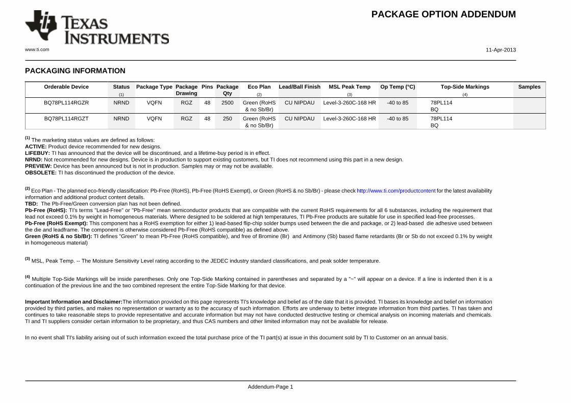
PACKAGING INFORMATION
Orderable Device Status(1)
Package Type PackageDrawing
Pins PackageQty
Eco Plan(2)
Lead/Ball Finish MSL Peak Temp(3)
Op Temp (°C) Top-Side Markings(4)
Samples
BQ78PL114RGZR NRND VQFN RGZ 48 2500 Green (RoHS& no Sb/Br)
CU NIPDAU Level-3-260C-168 HR -40 to 85 78PL114BQ
BQ78PL114RGZT NRND VQFN RGZ 48 250 Green (RoHS& no Sb/Br)
CU NIPDAU Level-3-260C-168 HR -40 to 85 78PL114BQ
(1) The marketing status values are defined as follows:ACTIVE: Product device recommended for new designs.LIFEBUY: TI has announced that the device will be discontinued, and a lifetime-buy period is in effect.NRND: Not recommended for new designs. Device is in production to support existing customers, but TI does not recommend using this part in a new design.PREVIEW: Device has been announced but is not in production. Samples may or may not be available.OBSOLETE: TI has discontinued the production of the device.
(2) Eco Plan - The planned eco-friendly classification: Pb-Free (RoHS), Pb-Free (RoHS Exempt), or Green (RoHS & no Sb/Br) - please check http://www.ti.com/productcontent for the latest availabilityinformation and additional product content details.TBD: The Pb-Free/Green conversion plan has not been defined.Pb-Free (RoHS): TI's terms "Lead-Free" or "Pb-Free" mean semiconductor products that are compatible with the current RoHS requirements for all 6 substances, including the requirement thatlead not exceed 0.1% by weight in homogeneous materials. Where designed to be soldered at high temperatures, TI Pb-Free products are suitable for use in specified lead-free processes.Pb-Free (RoHS Exempt): This component has a RoHS exemption for either 1) lead-based flip-chip solder bumps used between the die and package, or 2) lead-based die adhesive used betweenthe die and leadframe. The component is otherwise considered Pb-Free (RoHS compatible) as defined above.Green (RoHS & no Sb/Br): TI defines "Green" to mean Pb-Free (RoHS compatible), and free of Bromine (Br) and Antimony (Sb) based flame retardants (Br or Sb do not exceed 0.1% by weightin homogeneous material)
(3) MSL, Peak Temp. -- The Moisture Sensitivity Level rating according to the JEDEC industry standard classifications, and peak solder temperature.
(4) Multiple Top-Side Markings will be inside parentheses. Only one Top-Side Marking contained in parentheses and separated by a "~" will appear on a device. If a line is indented then it is acontinuation of the previous line and the two combined represent the entire Top-Side Marking for that device.
Important Information and Disclaimer:The information provided on this page represents TI's knowledge and belief as of the date that it is provided. TI bases its knowledge and belief on informationprovided by third parties, and makes no representation or warranty as to the accuracy of such information. Efforts are underway to better integrate information from third parties. TI has taken andcontinues to take reasonable steps to provide representative and accurate information but may not have conducted destructive testing or chemical analysis on incoming materials and chemicals.TI and TI suppliers consider certain information to be proprietary, and thus CAS numbers and other limited information may not be available for release.
In no event shall TI's liability arising out of such information exceed the total purchase price of the TI part(s) at issue in this document sold by TI to Customer on an annual basis.

TAPE AND REEL INFORMATION
*All dimensions are nominal
Device PackageType
PackageDrawing
Pins SPQ ReelDiameter
(mm)
ReelWidth
W1 (mm)
A0(mm)
B0(mm)
K0(mm)
P1(mm)
W(mm)
Pin1Quadrant
BQ78PL114RGZR VQFN RGZ 48 2500 330.0 16.4 7.3 7.3 1.5 12.0 16.0 Q2
BQ78PL114RGZT VQFN RGZ 48 250 180.0 16.4 7.3 7.3 1.5 12.0 16.0 Q2
PACKAGE MATERIALS INFORMATION
www.ti.com 12-Jan-2015
Pack Materials-Page 1

*All dimensions are nominal
Device Package Type Package Drawing Pins SPQ Length (mm) Width (mm) Height (mm)
BQ78PL114RGZR VQFN RGZ 48 2500 367.0 367.0 38.0
BQ78PL114RGZT VQFN RGZ 48 250 210.0 185.0 35.0
PACKAGE MATERIALS INFORMATION
www.ti.com 12-Jan-2015
Pack Materials-Page 2


IMPORTANT NOTICE
Texas Instruments Incorporated and its subsidiaries (TI) reserve the right to make corrections, enhancements, improvements and otherchanges to its semiconductor products and services per JESD46, latest issue, and to discontinue any product or service per JESD48, latestissue. Buyers should obtain the latest relevant information before placing orders and should verify that such information is current andcomplete. All semiconductor products (also referred to herein as “components”) are sold subject to TI’s terms and conditions of salesupplied at the time of order acknowledgment.TI warrants performance of its components to the specifications applicable at the time of sale, in accordance with the warranty in TI’s termsand conditions of sale of semiconductor products. Testing and other quality control techniques are used to the extent TI deems necessaryto support this warranty. Except where mandated by applicable law, testing of all parameters of each component is not necessarilyperformed.TI assumes no liability for applications assistance or the design of Buyers’ products. Buyers are responsible for their products andapplications using TI components. To minimize the risks associated with Buyers’ products and applications, Buyers should provideadequate design and operating safeguards.TI does not warrant or represent that any license, either express or implied, is granted under any patent right, copyright, mask work right, orother intellectual property right relating to any combination, machine, or process in which TI components or services are used. Informationpublished by TI regarding third-party products or services does not constitute a license to use such products or services or a warranty orendorsement thereof. Use of such information may require a license from a third party under the patents or other intellectual property of thethird party, or a license from TI under the patents or other intellectual property of TI.Reproduction of significant portions of TI information in TI data books or data sheets is permissible only if reproduction is without alterationand is accompanied by all associated warranties, conditions, limitations, and notices. TI is not responsible or liable for such altereddocumentation. Information of third parties may be subject to additional restrictions.Resale of TI components or services with statements different from or beyond the parameters stated by TI for that component or servicevoids all express and any implied warranties for the associated TI component or service and is an unfair and deceptive business practice.TI is not responsible or liable for any such statements.Buyer acknowledges and agrees that it is solely responsible for compliance with all legal, regulatory and safety-related requirementsconcerning its products, and any use of TI components in its applications, notwithstanding any applications-related information or supportthat may be provided by TI. Buyer represents and agrees that it has all the necessary expertise to create and implement safeguards whichanticipate dangerous consequences of failures, monitor failures and their consequences, lessen the likelihood of failures that might causeharm and take appropriate remedial actions. Buyer will fully indemnify TI and its representatives against any damages arising out of the useof any TI components in safety-critical applications.In some cases, TI components may be promoted specifically to facilitate safety-related applications. With such components, TI’s goal is tohelp enable customers to design and create their own end-product solutions that meet applicable functional safety standards andrequirements. Nonetheless, such components are subject to these terms.No TI components are authorized for use in FDA Class III (or similar life-critical medical equipment) unless authorized officers of the partieshave executed a special agreement specifically governing such use.Only those TI components which TI has specifically designated as military grade or “enhanced plastic” are designed and intended for use inmilitary/aerospace applications or environments. Buyer acknowledges and agrees that any military or aerospace use of TI componentswhich have not been so designated is solely at the Buyer's risk, and that Buyer is solely responsible for compliance with all legal andregulatory requirements in connection with such use.TI has specifically designated certain components as meeting ISO/TS16949 requirements, mainly for automotive use. In any case of use ofnon-designated products, TI will not be responsible for any failure to meet ISO/TS16949.
Products ApplicationsAudio www.ti.com/audio Automotive and Transportation www.ti.com/automotiveAmplifiers amplifier.ti.com Communications and Telecom www.ti.com/communicationsData Converters dataconverter.ti.com Computers and Peripherals www.ti.com/computersDLP® Products www.dlp.com Consumer Electronics www.ti.com/consumer-appsDSP dsp.ti.com Energy and Lighting www.ti.com/energyClocks and Timers www.ti.com/clocks Industrial www.ti.com/industrialInterface interface.ti.com Medical www.ti.com/medicalLogic logic.ti.com Security www.ti.com/securityPower Mgmt power.ti.com Space, Avionics and Defense www.ti.com/space-avionics-defenseMicrocontrollers microcontroller.ti.com Video and Imaging www.ti.com/videoRFID www.ti-rfid.comOMAP Applications Processors www.ti.com/omap TI E2E Community e2e.ti.comWireless Connectivity www.ti.com/wirelessconnectivity
Mailing Address: Texas Instruments, Post Office Box 655303, Dallas, Texas 75265Copyright © 2015, Texas Instruments Incorporated