Embed Size (px)
Citation preview

Power-Supply-Network Design in3D Integrated Systems
Michael B. Healy and Sung Kyu LimSchool of Electrical and Computer Engineering, Georgia Institute of Technology
777 Atlantic Dr. NW, Atlanta, GA 30332{mbhealy, limsk}@gatech.edu
Abstract—Three-dimensional integration (3D IC) technologyhas been gaining significant interest from the VLSI communityfor several years. However, layout-level explorations of the impactof 3D technology have only recently been introduced. This workexamines both static and dynamic power-supply noise in a layout-level 3D design prototype, and the impact of possible 3D-specificchanges to the power-supply network design and topology. Ourresults show that distributing power-supply TSVs throughoutthe design with finer pitch than the C4 supply bumps lowersboth IR-drop and dynamic noise in our 3D system. In fact,using a distributed TSV topology lowers dynamic noise by 13.3%compared to a 2D system with less total power dissipation. Wealso show several other 3D-specific supply network changes andtheir impact on both IR-drop and dynamic noise.
I. INTRODUCTION
Many players in both the VLSI industry and academiasee 3D stacking as a coming major trend. 3D stacking hasthe potential to reduce power consumption from off-chipcommunication, reduce wirelength and delay, and lower thecost of process integration. However, there remain manychallenges in the design of 3D ICs. Increases in volumetricpower density combine with larger thermal resistance betweenthe silicon layers and the heatsink could result in higheroperating temperatures and reductions in reliability. Smallerfootprints and larger package-level power consumption couldcause power-delivery problems. In this work we provide alayout-level examination of the design of 3D power deliverynetworks, and demonstrate that the unique environment of 3DICs can have a dramatic effect on both IR-drop and dynamicnoise in these networks.
We examine two types of power-supply noise in a layout-level prototype processor-on-memory stacked 3D system. IR-drop (sometimes referred to as ground-bounce) is the resistivevoltage drop in power and ground distribution networks causedby the dynamic and leakage power of ICs. Dynamic noisein power-supply networks results from transient changes indevice current demand interacting with inherent inductancein the power-delivery network. Continued device scaling hasresulted in reduction in supply voltages and increases in totalcurrent, which reduces power-supply-noise margins. Thesefactors are causing a larger and larger percentage of availablerouting resources to be dedicated to power supply distributionin high-performance designs, which can add significantly tocongestion problems and reduce the amount of functionalitythat can be packed into a unit area.
Many researchers have proposed optimization schemes fortraditional IC power network design. Previous work on powerdelivery networks for 3D systems has largely assumed astraightforward extension of 2D power delivery network de-sign. Huang et al. [1] presented a physical model of 3D powerdistribution networks. Jain et al. [2] extended the work of Guet al. [3] by examining the use of multi-story power deliveryin 3D ICs. Yu et al. [4] demonstrate an optimization schemefor supply-bump assignment and via insertion simultaneouslyconsidering both supply noise and temperature. Healy andLim [5] examined scaling trends in many-tier 3D power-delivery networks. All previous work assumes that supplybumps are aligned with TSVs in every case.
The overall goal of this work is to provide a layout-levelexploration of power delivery in 3D ICs and how it differsfrom traditional designs. Compared to prior efforts, we demon-strate the benefits of re-examining the unique capabilitiesof TSVs relative to package-level bumps. We also performour analysis using layout-level designs and strive to providerealistic results. Accordingly, we validate our model resultsusing commercial-grade sign-off IR-drop analysis software.The major contributions of this work are as follows:
∙ We present the first layout-level analysis of 3D powerdistribution networks that is validated using commercialtools.
∙ We demonstrate improve power-supply noise by spread-ing power and ground distribution TSVs away from thepower and ground supply bumps in designs with non-uniform power dissipation.
∙ We examine other 3D-specific techniques for improvingpower-supply noise and demonstrate their effectivenessusing our framework.
II. 3D AND FLIP-CHIP POWER NETS
High performance 3D systems will generally use flip-chip style packaging to increase off-chip interconnect densityand reduce parasitics. Flip-chip power distribution systemsare commonly laid out as grids. High-level metal layersare reserved for laying out a coarse-grained grid with largewires that connects a regular array of power and ground C4bumps. A fine-grained mesh provides local distribution andconnects to lower-level-metal power rings or standard-cell rowdistribution wiring. Most commercial products today have C4
978-1-61284-914-0/11/$26.00 ©2011 IEEE 372 12th Int'l Symposium on Quality Electronic Design

P/G bump
P/G TSVs
P/G wires (thick)
Fig. 1. Bumps, TSVs, and wires in a 3D P/G network
bump pitches around 100 to 200𝜇𝑚, however, researchers havedemonstrated micro-bumps with pitches below 10𝜇𝑚.
For 3D systems, each tier will contain its own powerdistribution network. These networks will all be interconnectedusing TSVs. Figure 1 shows the general topology of a 3Dpower distribution network. The inter-layer resistance betweenadjacent tiers should be close to that of the C4 bumps tomaintain reliable power and ground voltages. The resistanceof individual C4 bumps is on the order of 5𝑚Ω. Additionally,TSVs should be much smaller than the C4 bumps or largeamounts (25% or more) of die area will become unusable.
TSVs can be manufactured in many different sizes. Diame-ters of less than 1𝜇𝑚 have been shown in the literature. Powerand ground TSVs should be large to have low resistance, butsignal TSVs should be small to increase interconnect densityand reduce parasitic capacitance. Manufacturing multiple TSVsizes on a single die would increase cost and reduce yield.Therefore, it will likely be necessary to use a single TSV sizefor both power distribution and signal wiring.
In this work it is assumed that only one TSV size isavailable, and the TSV size is optimized for signals. There areseveral potential combinations of TSV distribution that couldbe used to deliver power. Figure 2 shows two of the basicchoices we investigate thoroughly in this paper.
∙ clustered topology: multiple small TSVs are clusteredover the C4 pads for both power and ground distribution.
∙ distributed topology: multiple small TSVs are spreadevenly throughout the die.
The combined resistance of all the TSVs is assumed to be thesame for both of the topologies.
III. PROTOTYPE LAYOUT
The prototype layout used in our simulations is based on adesign targeted at demonstrating extreme memory bandwidthusing 3D interconnects. Our design is a many-core processorcomposed of an array of simple cores connected with anearest-neighbor communication mesh. Each core has eightbanks of dedicated SRAM directly stacked above it in twoseparate tiers. The core tier contains a 10× 10 array of cores.
The 100-core prototype processor was designed using a130-nm standard cell library from Global Foundries. For thephysical design we used Cadence’s SOC Encounter automated
Bulk ActiveLayer
TSV
C4
Core
Mem 1
Mem 2
Bulk ActiveLayer
TSV
C4
Core
Mem 1
Mem 2
Clustered Distributed
Fig. 2. Two TSV topologies for power distribution. C4 bumps are shown inblack and P/G TSVs in green. The combined resistance of all TSVs in eachtopology is equal.
i-MEM
RF
Fig. 4. The power map for one core of our processor. The maximum totalpower consumption per core is 65.5𝑚𝑊 .
place and route tool. The layouts for a single core and asingle memory tile are shown in Figure 3. We also highlightthe areas in the layout reserved for ground TSV connections.The distribution of connection points is irregular due to theconstraints of the layout, especially the locations of the hardmemory macros. For the distributed TSV topology, TSVs arelocated at all of the potential locations. In the clustered TSVtopology, all of the TSVs are grouped into the center position,over the C4 bump. The power TSV locations are similarlydistributed in an offset fashion, the main difference is thatthe power C4 bumps are at the corners of the core, while theground C4 bump is in the center. Each location is capable ofaccepting a 6𝜇𝑚 diameter via-first TSV, while the locationsover the C4 bumps (the center and near the corners) arecapable of accepting 25 or more of these TSVs.
The single-core and single-tile layouts are both 560𝜇𝑚square. The core-to-core and tile-to-tile pitch is 590𝜇𝑚 toaccommodate the inter-core logic and communication, as wellas the power distribution from the C4 bumps. The full 100-core and 100-tile layers are approximately 6𝑚𝑚 square. Themaximum total power dissipation for the system (one core tier+ two memory tiers) is approximately 13.2𝑊 . Figure 4 showsthe power map for a single core. The power dissipation ofthis design is not extreme, however the high volumetric powerdensity could be a problem for traditional heatsinks. For thiscase micro-fluidic channels [6], [5] have been shown to be aneffective method for cooling large-scale 3D chip stacks.

single core layout
possible ground TSV locationsground C4
single memory tile
Fig. 3. Layout of a single core and single memory tile from our 100-core processor. The possible ground distribution TSV locations are highlighted in red.The ground C4 bump in the center of the core is indicated. The power C4 bumps are near the corners of the core.
IV. 3D IR-DROP ANALYSIS
A. Methodology
Layout-level IR-drop values are computed by perform-ing power consumption simulations, either statistical orsimulation-driven, to obtain gate- and module-level powerconsumption values. The consumption values are then dividedby the nominal supply voltage, in our case 1.5𝑉 , to obtaingate- and module-level current consumption values. Next,parasitic extraction is performed on the layout to obtain aSPICE netlist that models the power distribution network. Ourexperiments were performed using Cadence’s QRC transistor-level extraction tool. The current consumption values arethen connected to the nodes representing the correspondingtransistors belonging to the appropriate gates and modules.For traditional 2D ICs the netlist is then simulated using apower network simulator, in our case Cadence’s UltraSim.Figure 5 shows the analysis flow 2D netlists. In 3D designsthe previously described steps are performed once for eachtype of tier (core, memory, etc.). The tier-type SPICE modelsare replicated for each instance of that tier-type and thenconnected using a resistive TSV model.
Simulation of power distribution networks is a generallydifficult problem for traditional ICs. These networks cancontain tens of millions of nodes. 3D stacking exacerbatesthe problem even further. Given the extreme regularity of theprototype design that is examined in this work, we mitigatesome of the extreme memory and execution-time requirementsof power network simulation by only simulating a 5× 5 arrayof cores instead of the full 10 × 10 array. We stress thatour design is extremely regular and so this reduction shouldonly impact the accuracy of our analysis in a minor way.Simulations indicate that this introduces approximately 3%error in our results.
layout
CalibreLVS
annotatedGDSII
CadenceQRC
SPICEnetlist
CadenceVoltageStorm
powerconsumption
translate transistorsto current sources
tier-level netlist
Fig. 5. The analysis flow used to obtain the tier-level netlist for IR-dropanalysis. This flow is performed multiple times for each tier type, then thenetlists are connected together with a TSV model for 3D analysis.
B. Validation
We compare the results for a 2D layout to Cadence’sVoltageStorm sign-off power noise analysis tool to validatethe IR-drop analysis flow described above. The results ofour analysis flow are within 4% of the values reported byVoltageStorm. We were also able to create a method fortricking VoltageStorm into performing 3D analysis for two-tier stacks.
First we create an ICT file, a process technology descriptionfile, that contains a description of all of the metal layers intwo tiers. The metal and dielectric layers are renamed sothat the tier number is embedded in the name. For example,“METAL1” becomes “METAL1 1” and “METAL1 2.” Then,a techfile is created using Cadence’s TechGen based on thenew ICT file. Next, we modify the LEF files provided bythe foundry that describe the technology, standard cells, and

Fig. 6. A depiction of the ICT file that contains metal layers for two tiersof a 3D stack. The ICT file is used to compile a techfile used for parasiticextraction by VoltageStorm for our 3D IR-drop verification flow.
macros. The DEF and instance power files for the designsof each tier are also modified in the same way. Each file isessentially duplicated so that there is one version for the firsttier and one version for the second tier. The modificationsamount to renaming the objects and metal layers in the sameway that the ICT file is modified. To include detailed analysisof the macro blocks, we also modify their GDSII files. Wefirst convert the GDSII to GDT, an ascii-version of the binaryGDSII data. Then we map all of the GDSII layer numbers forthe metal layers into a non-overlapping number space. Themodified GDT is then converted back to GDSII. The XTCextraction tool is then given a GDSII layer map file that mapsthe appropriate layer numbers to the correct tier’s metal layersfor each macro.
Using the above method we were able to match the 3D IR-drop results from VoltageStorm within 4%. Figure 6 shows adepiction from Cadence’s ViewICT tool of the modified ICTfile containing metal layers in two dies. Note that the seconddie does not have a substrate layer. This is a limitation ofthe tool, due to the fact that it was not designed with 3Ddesigns in mind. However, for power/ground network analysisthe substrate can largely be ignored. For these experiments wecreated a face-to-back style 3D design, however, this techniqueis general enough to apply to face-to-face 3D designs as well.
V. 3D DYNAMIC NOISE ANALYSIS
Layout-level dynamic noise values are computed using thepower consumption values and parasitic extracted networksobtained for IR-drop analysis with added decoupling capac-itors. We create triangular current demand waveforms [7](Figure 7) for each transistor such that the average powerconsumption matches the value obtained for IR-drop analysis.The triangular waveforms for each gate are delayed by arandom amount such that the majority of them start near thebeginning of the cycle. The random delays are distributed ina Gaussian fashion about zero and then the absolute value ofthe delay is used for the real current waveform. Our dynamicnoise numbers are obtained by performing transient simulation
0 50 ps 150 ps 300 ps
IloadImax
...
Fig. 7. The current waveform used for each transistor for dynamic noiseanalysis. A random delay is added to the start of the waveform for each gate’stransistors.
TABLE IEFFECTIVE INDUCTANCE VALUES IN 𝑝𝐻 FOR POWER DISTRIBUTION
TSVS. THE TSV DIMENSIONS ARE IN 𝜇𝑚.
TSV Dimensions Clustered Distributed3× 3× 10𝜇𝑚 0.829 𝑝𝐻 0.014 𝑝𝐻6× 6× 20𝜇𝑚 1.600 𝑝𝐻 0.027 𝑝𝐻
10× 10× 33𝜇𝑚 2.500 𝑝𝐻 0.041 𝑝𝐻15× 15× 50𝜇𝑚 3.600 𝑝𝐻 0.058 𝑝𝐻
of a repeating pattern of current demand with a cycle time of300𝑝𝑠. The peak of the voltage swing is recorded as the noisevalue after the swings have stabilized.
Ultrasim’s power network simulation engine does not handlelarge-scale transient simulation well, so we used a customSPICE simulator based on Modified Nodal Analysis [8], whichreturns results within 2% of HSPICE. For our simulations weuse a step size of 1𝑝𝑠. TSV inductance may also be an impor-tant contributor to dynamic noise. We modeled several sizesand arrangements of TSVs using Synopsys’ inductance extrac-tor Raphael. The results of our TSV inductance simulationsare shown in Table I. The distributed TSV topology resultsin effective inductance values about two orders of magnitudesmaller than the clustered TSV topology. The default TSV sizeused in most of our simulations is 6× 6× 20𝜇𝑚.
VI. RESULTS
First, we compare our 3D prototype system with a 2Dsystem containing a single layer with 100 cores. The IR-dropand dynamic noise results are shown in Figure 8. The graphshows that the 3D system with the clustered TSV topologyresults in higher maximum IR-drop and dynamic noise inthe core layer. This is expected due to the additional TSVparasitics between the package-level power-supply bumps andthe extra power consumed by the memory layers. However,the 3D system using the distributed TSV topology resultsin 13.3% lower IR-drop and dynamic noise than the 2Dsystem, even though the 3D system dissipates more power.The improvements in power-supply noise seen when using thedistributed TSV topology are enabled by the sharing of noise“slack” between the memory layers and the core layers. Thiscan be seen in Figure 8 by comparing the relative noise levelsof the memory layers between the clustered and distributedTSV topologies. The distributed TSV topology trades-offlower maximum system-level supply noise with higher supply-noise levels in the memory layers.
Next, we show the results of modifying the size of theTSVs used to deliver power in our prototype 3D system. Thisanalysis is accomplished by modifying the resistances and

Core Only Clustered Distributed Core Only Clustered Distributed0
50
100
150
200
250 Noise Value (mV) Core Mem 1 Mem 2
IR-Drop Dynamic Noise2D 3D 3D 2D 3D 3D
Fig. 8. A comparison of the IR-drop and dynamic noise results for a2D system with only the core tier and 3D systems with the clustered anddistributed TSV topologies. The black line at 150𝑚𝑉 represents the 10%noise margin.
3x3 6x6 10x10 15x150
50
100
150
200
250 Dynamic Noise (mV) Clustered Distributed
TSV Size (um)
DefaultTSV Size
Fig. 9. The dynamic noise in the three-layer system with both the clusteredand distributed TSV topologies. Results for several different TSV sizes areshown.
inductances representing the TSVs connecting neighboringtiers. Figure 9 shows the impact on dynamic noise of usingfour different sizes of TSVs. For this three-layer 3D system,the impact on power-supply noise of using different TSV sizesis relatively negligible. The impact is more significant for thedistributed topology than for the clustered topology. However,TSV size will have a more significant impact on the actuallayout itself, as well as the timing of the 3D signal nets. Thetrends for IR-drop are similar to those for dynamic noise.
Figure 10 shows IR-drop and dynamic noise results forchanging the number of bumps per core from the default (twobumps per core) to eight bumps per core. The results showthat decreasing the C4 pitch has a significant impact on thenoise results. The benefits of the distributed topology dropwith more bumps per core because the number of TSVs is notincreasing in this comparison. The trends are similar betweenIR-drop and dynamic noise.
The different power dissipation levels of the various tiersin the 3D stack affect the improvements caused by using thedistributed TSV topology versus the clustered TSV topology.To examine this in more detail we modified the power con-sumption of each tier such that the total power consumptionof the stack remained constant. The supply-noise results arethen plotted against the ratio of power dissipation betweenthe core and memory tiers. The supply-noise results for thisset of simulations is shown in Figure 11. Additionally, the
0
50
100
150
200
250Noise Value (mV) Clustered Distributed
Number of Bumps/CoreIR-Drop Dynamic
Default Default
2 Bumps 8 Bumps 2 Bumps 8 Bumps
Fig. 10. The impact on IR-drop and dynamic noise of increasing the numberof bumps from two per core to eight per core.
120
150
180
210
240
0 0.2 0.4 0.6 0.8 1 1.2
Power Dissipation Ratio
Dynamic Noise (mV) ClusteredDistributed
Fig. 11. The effect on dynamic noise of modifying the power dissipation ratiobetween the core and memory tiers. The total power consumption remainsthe same. The inflection point at 0.6 indicates the point where all three tiersdissipate the same amount of power.
actual percentage improvement in supply-noise is shown inFigure 12. The graphs show that when the power dissipationratio between the memory and core tiers results in even powerdissipation among all tiers the benefit of the distributed TSVtopology is the lowest. As the ratio diverges from this valuethe improvement of the distributed topolgy increases up to20%.
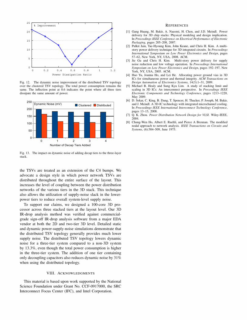
Finally, Figure 13 shows the impact on dynamic noise ofadding decap tiers to the three-layer stack. Adding a singledecap tier improves the dynamic noise below the 150𝑚𝑉 noisemargin for the distributed TSV topology. Adding four decaptiers to the clustered topology (more than doubling the numberof tiers stacked together) does not reduce the supply-noisebelow the 10% noise margin. These results indicate once morethat the distributed TSV topology generally results in improvedsupply-noise performance. In fact, the addition of decap tiers isthe only modification to the power-supply network that reducesthe dynamic noise below the 10% noise margin.
VII. CONCLUSIONS
In this work we have explored 3D power delivery networkdesign and shown that IR-drop and dynamic noise can be im-proved in these systems by exploiting the particular attributesof power supply TSVs that are unique compared to those of C4supply bumps. Previous works have assumed a straightforwardextension of traditional power supply network design in which
0
5
10
15
20
25
0 0.2 0.4 0.6 0.8 1 1.2
Power Dissipation Ratio
% Improvement
Fig. 12. The dynamic noise improvement of the distributed TSV topologyover the clustered TSV topology. The total power consumption remains thesame. The inflection point at 0.6 indicates the point where all three tiersdissipate the same amount of power.
0 1 2 3 40
50
100
150
200
250Dynamic Noise (mV) Clustered Distributed
Number of Decap Tiers Added
Fig. 13. The impact on dynamic noise of adding decap tiers to the three-layerstack.
the TSVs are treated as an extension of the C4 bumps. Weadvocate a design style in which power network TSVs aredistributed throughout the entire surface of the layout. Thisincreases the level of coupling between the power distributionnetworks of the various tiers in the 3D stack. This techniquealso allows the utilization of supply-noise slack in the lower-power tiers to reduce overall system-level supply noise.
To support our claims, we designed a 100-core 3D pro-cessor across three stacked tiers at the layout level. Our 3DIR-drop analysis method was verified against commercial-grade sign-off IR-drop analysis software from a major EDAvendor at both the 2D and two-tier 3D level. Detailed staticand dynamic power-supply-noise simulations demonstrate thatthe distributed TSV topology generally provides much lowersupply noise. The distributed TSV topology lowers dynamicnoise for a three-tier system compared to a non-3D systemby 13.3%, even though the total power consumption is higherin the three-tier system. The addition of one tier containingonly decoupling capacitors also reduces dynamic noise by 31%when using the distributed topology.
VIII. ACKNOWLEDGMENTS
This material is based upon work supported by the NationalScience Foundation under Grant No. CCF-0917000, the SRCInterconnect Focus Center (IFC), and Intel Corporation.
REFERENCES
[1] Gang Huang, M. Bakir, A. Naeemi, H. Chen, and J.D. Meindl. Powerdelivery for 3D chip stacks: Physical modeling and design implication.In Proceedings IEEE Conference on Electrical Performance of ElectronicPackaging, pages 205–208, 2007.
[2] Pulkit Jain, Tae-Hyoung Kim, John Keane, and Chris H. Kim. A multi-story power delivery technique for 3D integrated circuits. In ProceedingsInternational Symposium on Low Power Electronics and Design, pages57–62, New York, NY, USA, 2008. ACM.
[3] Jie Gu and Chris H. Kim. Multi-story power delivery for supplynoise reduction and low voltage operation. In Proceedings InternationalSymposium on Low Power Electronics and Design, pages 192–197, NewYork, NY, USA, 2005. ACM.
[4] Hao Yu, Joanna Ho, and Lei He. Allocating power ground vias in 3DICs for simultaneous power and thermal integrity. ACM Transactions onDesign Automation of Electronics Systems, 14(3):1–31, 2009.
[5] Michael B. Healy and Sung Kyu Lim. A study of stacking limit andscaling in 3D ICs: An interconnect perspective. In Proceedings IEEEElectronic Components and Technology Conference, pages 1213–1220,May 2009.
[6] D. Sekar, C. King, B. Dang, T. Spencer, H. Thacker, P. Joseph, M. Bakir,and J. Meindl. A 3D-IC technology with integrated microchannel cooling.In Proceedings IEEE International Interconnect Technology Conference,pages 13–15, 2008.
[7] Q. K. Zhou. Power Distribution Network Design for VLSI. Wiley-IEEE,2004.
[8] Chung-Wen Ho, Albert E. Ruehli, and Pierce A Brennan. The modifiednodal approach to network analysis. IEEE Transactions on Circuits andSystems, (6):504–509, June 1975.