Embed Size (px)
Citation preview

DAR ES SALAAM INSTITUTE OF TECHNOLOGY
DEPARTMENT OF ELECTRONICS AND TELECOMMUNICATION
ETT 05213: ELECTRONIC SYSTEM COMPUTER AIDED DESIGN
PILI JAMES 140627193619.
TELECOM 1.
AIM
To design a Dual DC power supply of DC output power Po=290 mV, DC output
voltage Vo(avg) =+12V and -12V, with AC mains Vs=240V/60Hz with the following
functionality;
I. On/Off switch
II. Current flow direction
III. Output results displayed on Oscilloscope
IV. Output results displayed on Graph
V. Voltmeter/Ammeter measurement.
THEORY.
Bellow is the block diagram for the Regulated DC Power Supply.
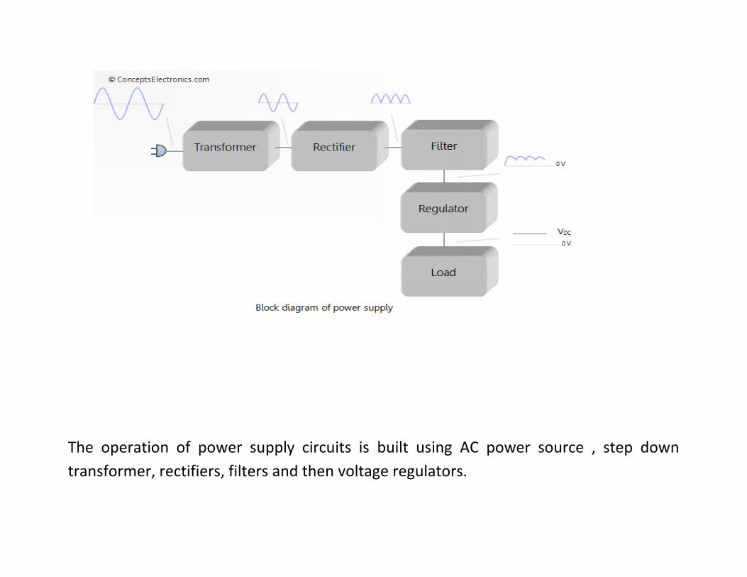
The operation of power supply circuits is built using AC power source , step down
transformer, rectifiers, filters and then voltage regulators.
An Ac voltage from Ac source is stepped down by transformer .Then the bridge rectifier
circuit convert the Ac voltage into pulsating DC voltage. The capacitor filter circuit filter
out the ripple voltage from rectified voltage to get non-pulsating voltage. In order to get
the steady DC voltage regardless the variation in AC power source ,the Voltage regulator
is required for the same purpose. LM7812 LM7912 regulators are used to get the fixed
+12V and -12V output voltage respectively.
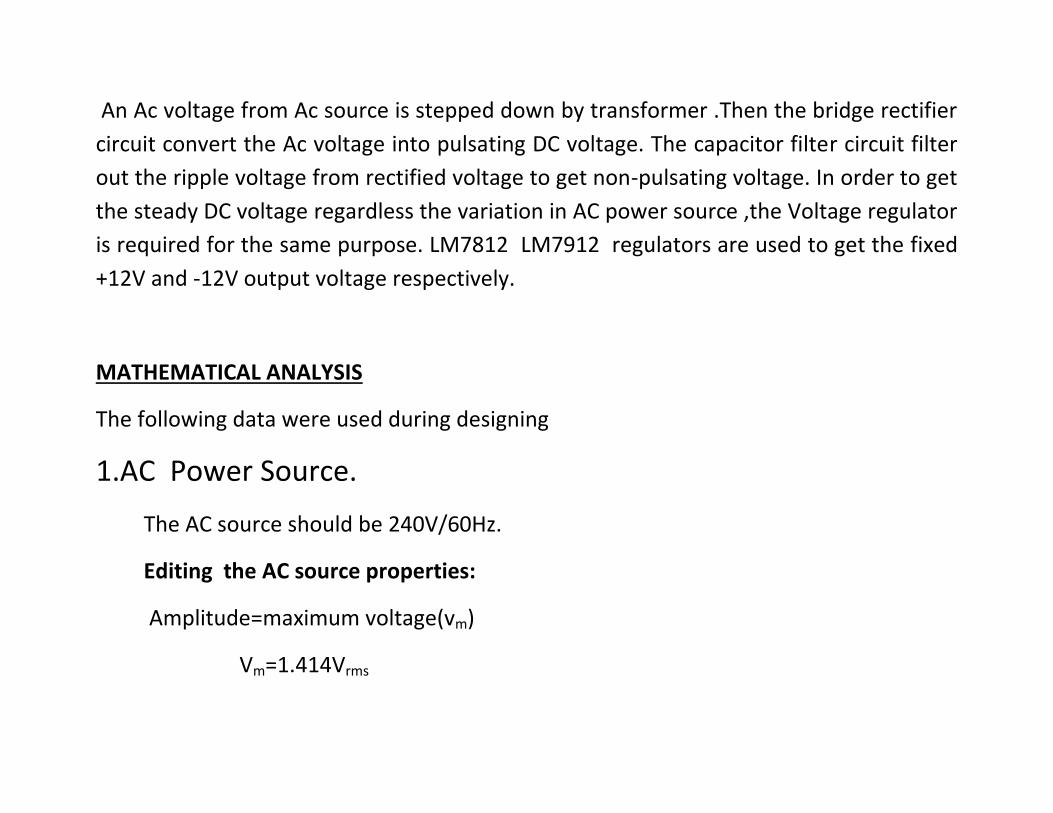
MATHEMATICAL ANALYSIS
The following data were used during designing
1.AC Power Source.
The AC source should be 240V/60Hz.
Editing the AC source properties:
Amplitude=maximum voltage(vm)
Vm=1.414Vrms
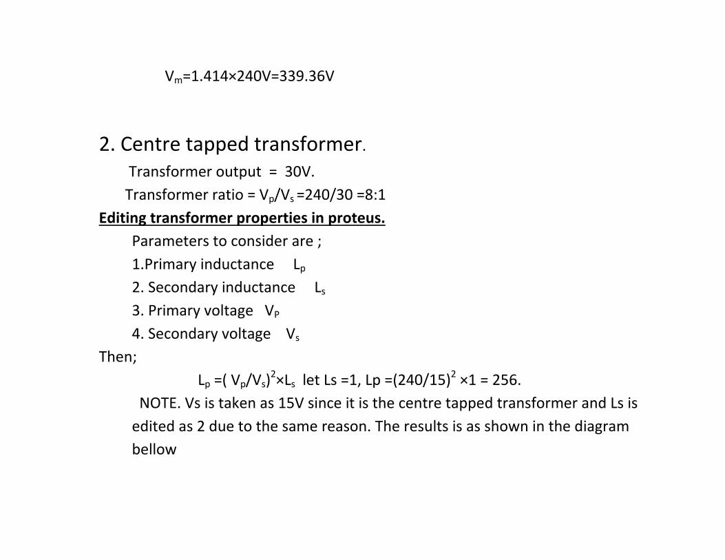
Vm=1.414×240V=339.36V
2. Centre tapped transformer.
Transformer output = 30V.
Transformer ratio = Vp/Vs =240/30 =8:1
Editing transformer properties in proteus.
Parameters to consider are ;
1.Primary inductance Lp
2. Secondary inductance Ls
3. Primary voltage VP
4. Secondary voltage Vs
Then;
Lp =( Vp/Vs)2×Ls let Ls =1, Lp =(240/15)2 ×1 = 256.
NOTE. Vs is taken as 15V since it is the centre tapped transformer and Ls is
edited as 2 due to the same reason. The results is as shown in the diagram
bellow
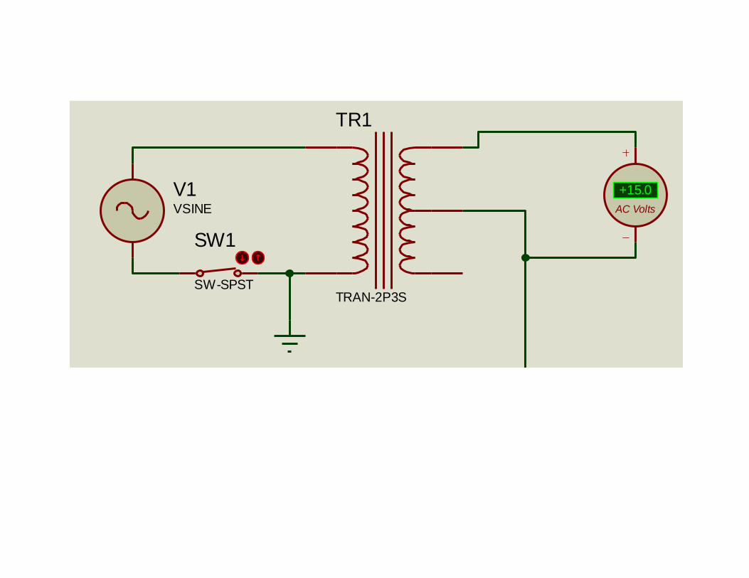
V1VSINE
TR1
TRAN-2P3S
SW1
SW-SPST
AC Volts
+15.0
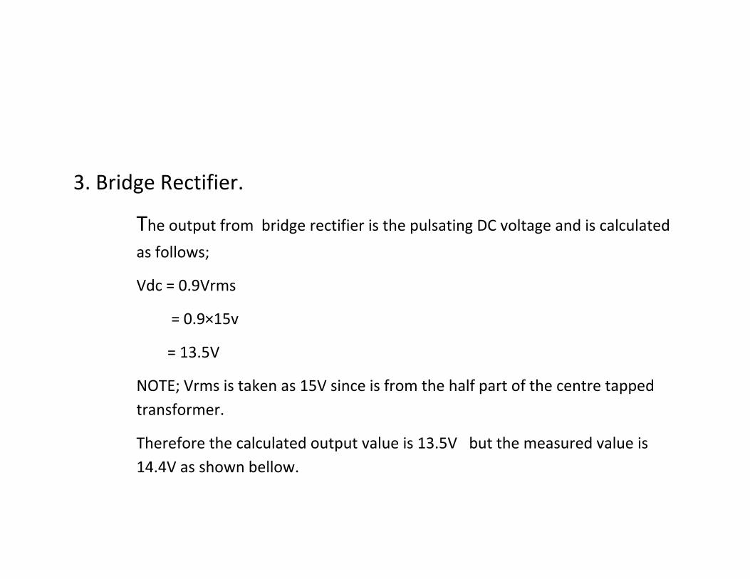
3. Bridge Rectifier.
The output from bridge rectifier is the pulsating DC voltage and is calculated
as follows;
Vdc = 0.9Vrms
= 0.9×15v
= 13.5V
NOTE; Vrms is taken as 15V since is from the half part of the centre tapped
transformer.
Therefore the calculated output value is 13.5V but the measured value is
14.4V as shown bellow.
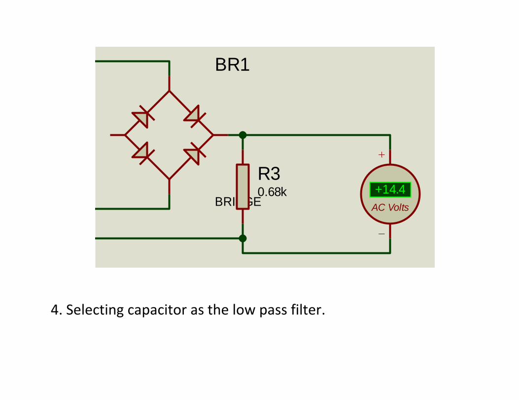
4. Selecting capacitor as the low pass filter.
BR1
BRIDGE
R30.68k
AC Volts
+14.4
Given that; Output power Po = 290mW.
And Po = Vo2/RL, where ,RL is the load resistance. Then,
RL = Vo2/po
RL = 13.52/290mW = 628.45Ω or 0.628kΩ.
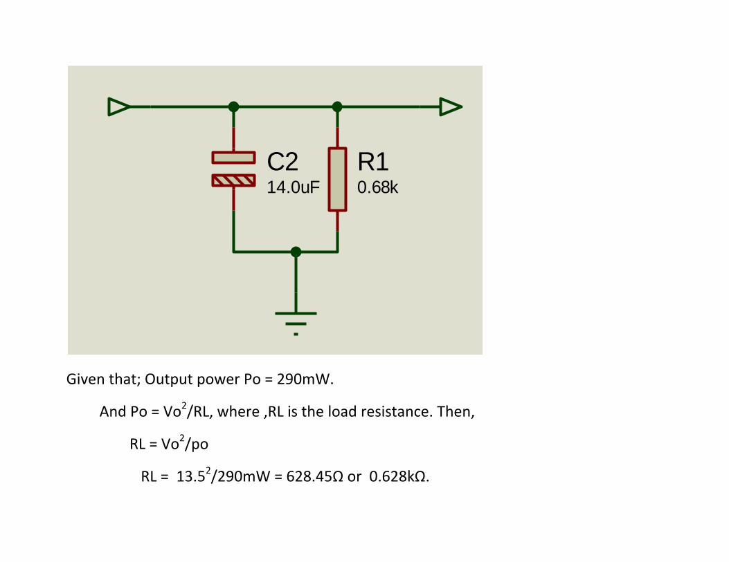
R10.68k
C214.0uF
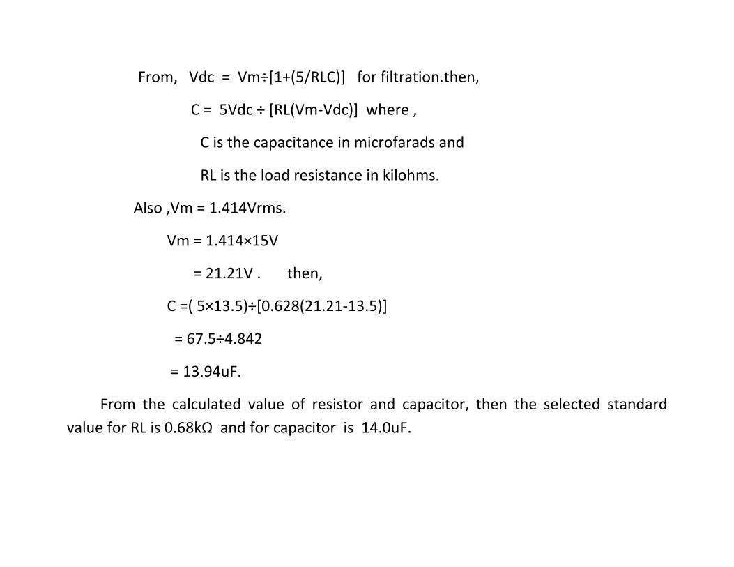
From, Vdc = Vm÷[1+(5/RLC)] for filtration.then,
C = 5Vdc ÷ [RL(Vm-Vdc)] where ,
C is the capacitance in microfarads and
RL is the load resistance in kilohms.
Also ,Vm = 1.414Vrms.
Vm = 1.414×15V
= 21.21V . then,
C =( 5×13.5)÷[0.628(21.21-13.5)]
= 67.5÷4.842
= 13.94uF.
From the calculated value of resistor and capacitor, then the selected standard
value for RL is 0.68kΩ and for capacitor is 14.0uF.
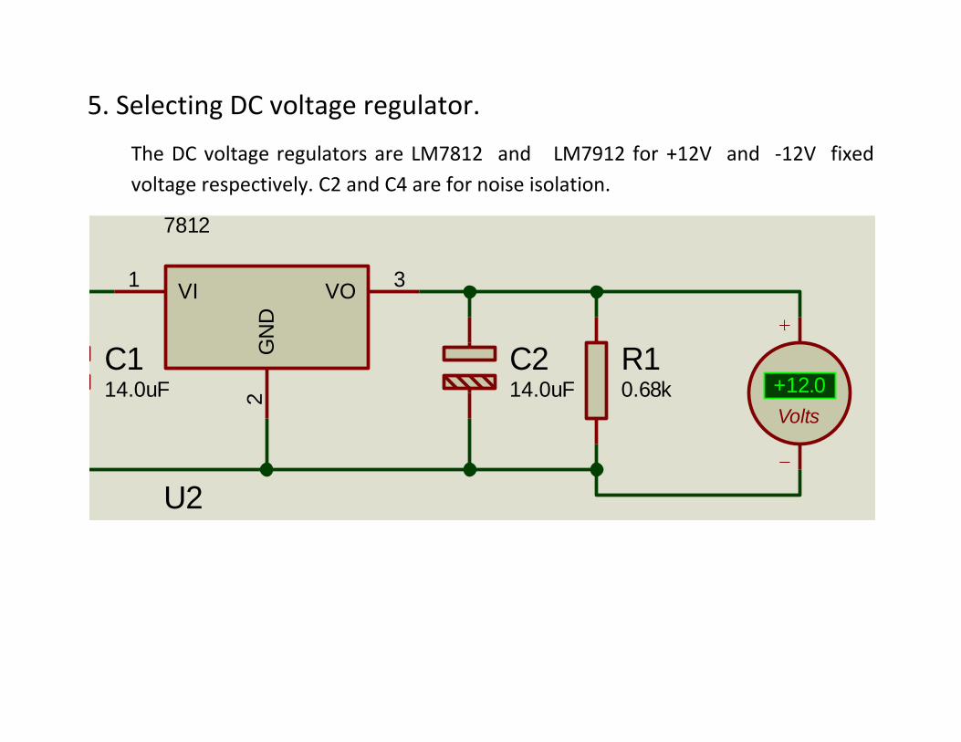
5. Selecting DC voltage regulator.
The DC voltage regulators are LM7812 and LM7912 for +12V and -12V fixed
voltage respectively. C2 and C4 are for noise isolation.
C114.0uF
R10.68k
VI1
VO3
GN
D2
U17812
C214.0uF
VI2
VO3
GN
D1
U27912
Volts
+12.0
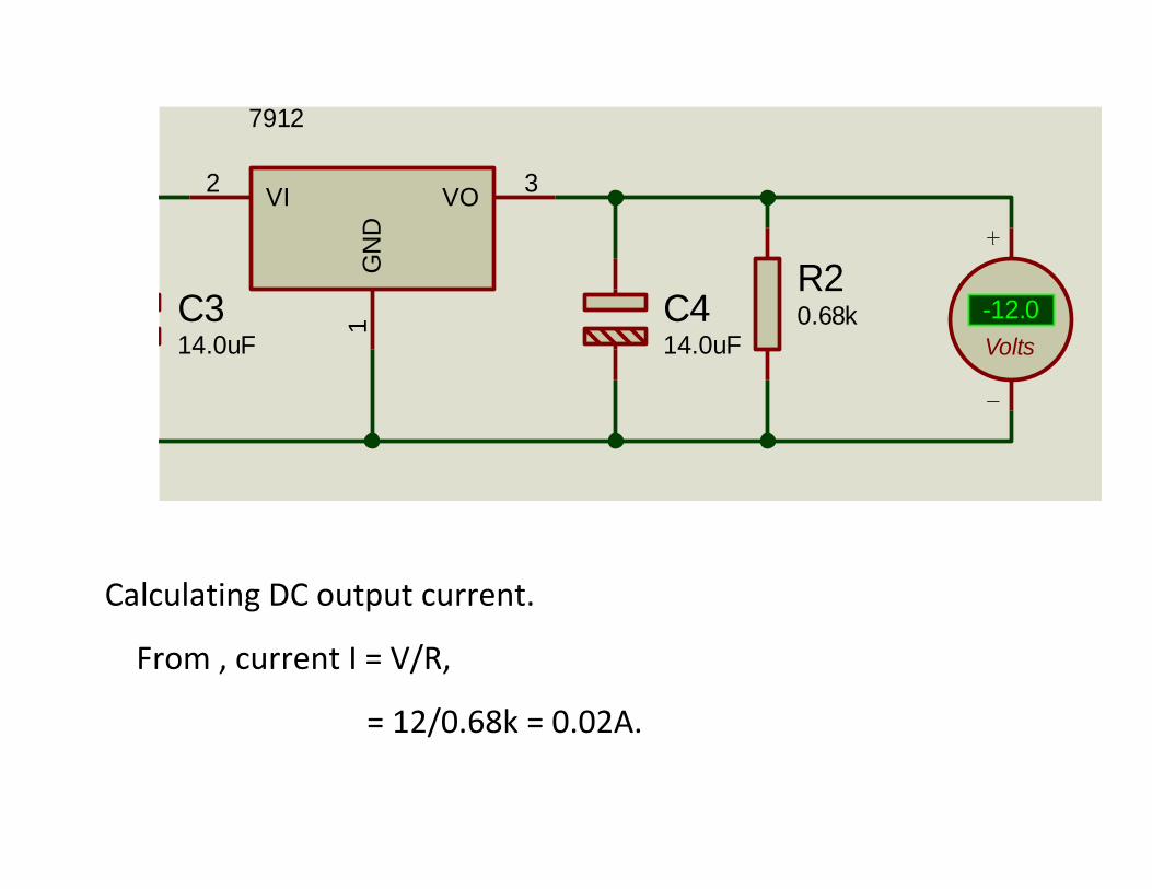
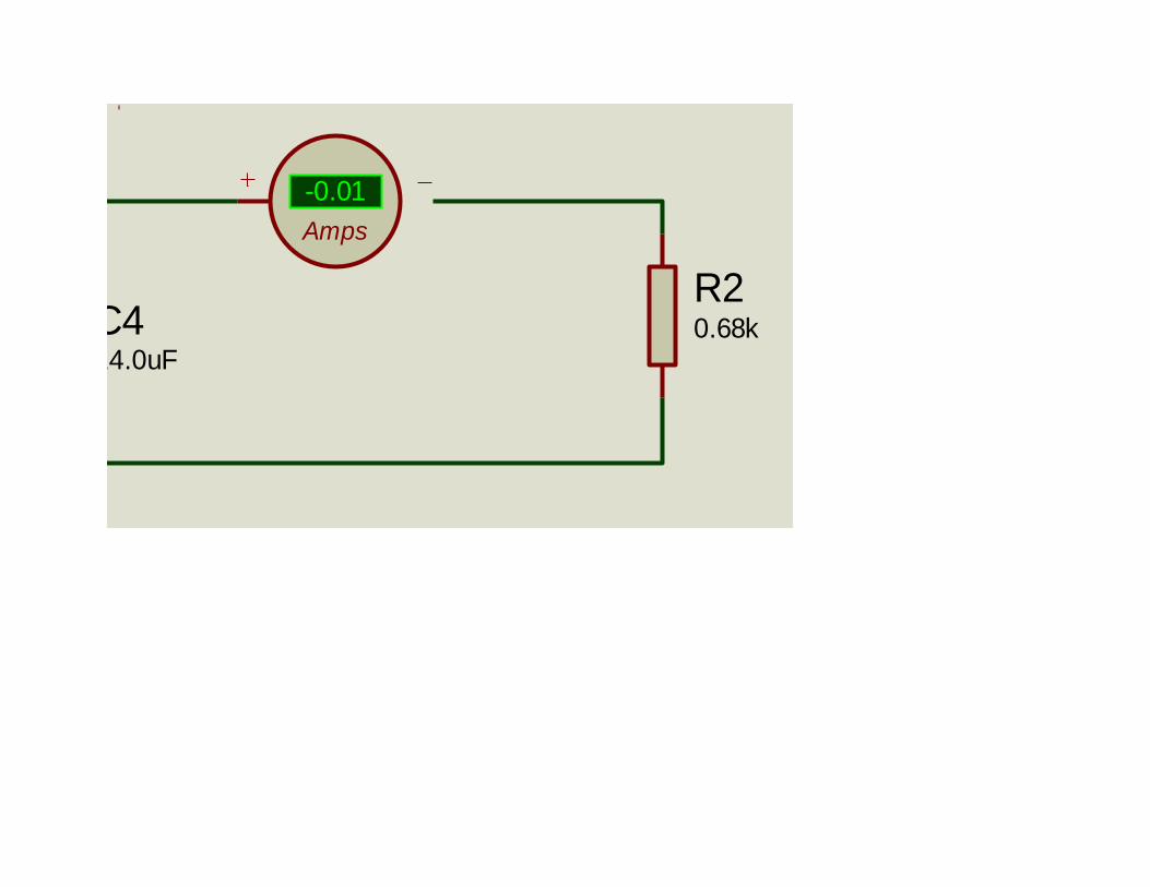
Calculating DC output current.
From , current I = V/R,
= 12/0.68k = 0.02A.
C314.0uF
C414.0uF
R20.68k
VI2
VO3
GN
D1
U27912
Volts
-12.0
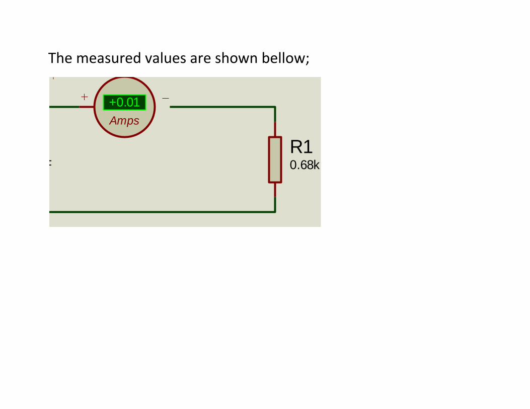
The measured values are shown bellow;
R10.68k
C214.0uF
Amps
+0.01
C414.0uF
R20.68k
Amps
-0.01
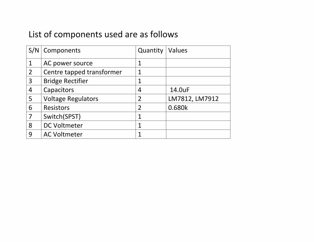
List of components used are as follows
S/N Components Quantity Values
1 AC power source 1
2 Centre tapped transformer 1 3 Bridge Rectifier 1 4 Capacitors 4 14.0uF 5 Voltage Regulators 2 LM7812, LM7912
6 Resistors 2 0.680k 7 Switch(SPST) 1 8 DC Voltmeter 1 9 AC Voltmeter 1
THE PROPOSED CIRCUIT DIAGRAM
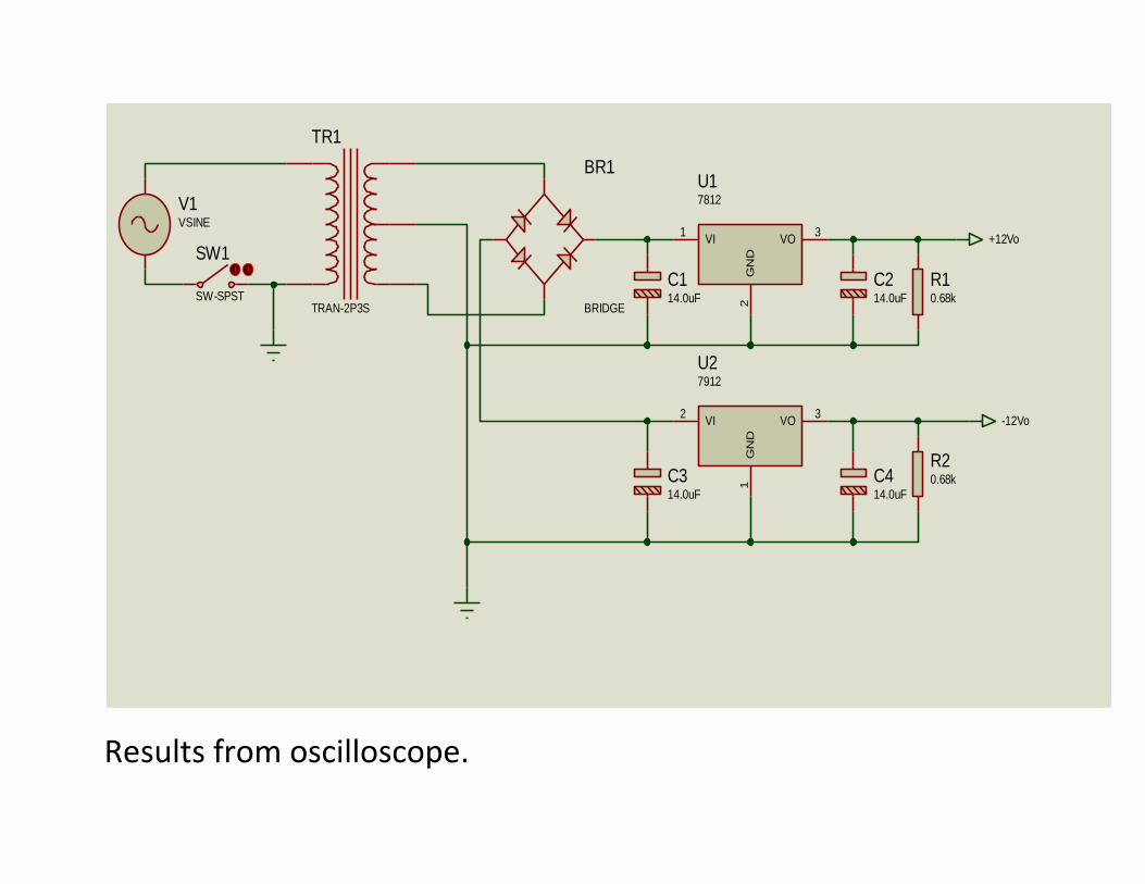
Results from oscilloscope.
V1VSINE
TR1
TRAN-2P3S
SW1
SW-SPST
BR1
BRIDGE
C114.0uF
R10.68k
VI1
VO3
GN
D2
U17812
C214.0uF
C314.0uF
C414.0uF
R20.68k
VI2
VO3
GN
D1
U27912
+12Vo
-12Vo
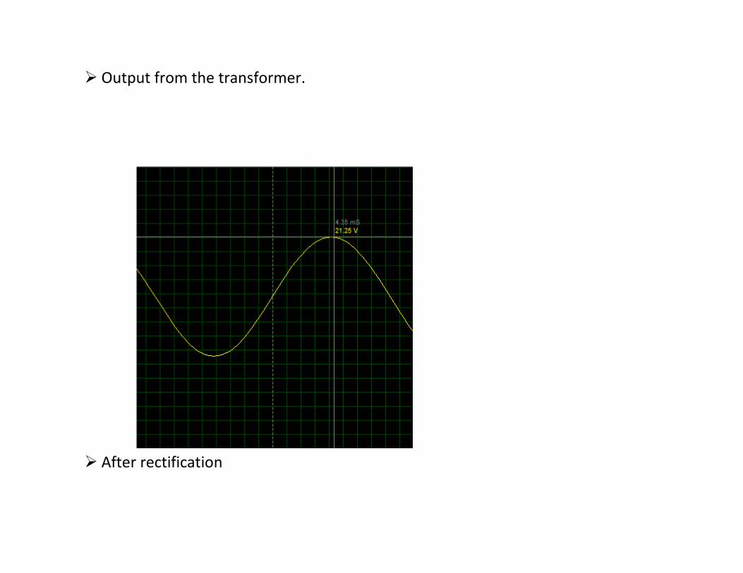
Output from the transformer.
After rectification
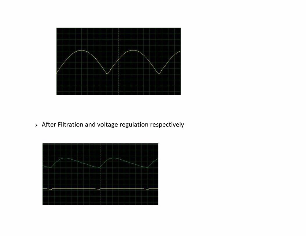
After Filtration and voltage regulation respectively
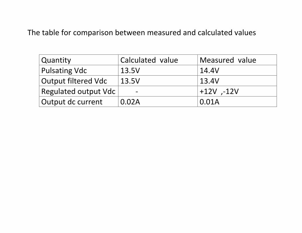
The table for comparison between measured and calculated values
Quantity Calculated value Measured value Pulsating Vdc 13.5V 14.4V Output filtered Vdc 13.5V 13.4V Regulated output Vdc - +12V ,-12V Output dc current 0.02A 0.01A


![Amani Jamal Areej Alhothali arXiv:2111.05671v1 [cs.CL] 10](https://img.pdfslide.us/doc/110x75/62771c6dce7fb93448419174/amani-jamal-areej-alhothali-arxiv211105671v1-cscl-10-.jpg)