Embed Size (px)
Citation preview
HAL Id: hal-02381699https://hal.archives-ouvertes.fr/hal-02381699
Submitted on 26 Nov 2019
HAL is a multi-disciplinary open accessarchive for the deposit and dissemination of sci-entific research documents, whether they are pub-lished or not. The documents may come fromteaching and research institutions in France orabroad, or from public or private research centers.
L’archive ouverte pluridisciplinaire HAL, estdestinée au dépôt et à la diffusion de documentsscientifiques de niveau recherche, publiés ou non,émanant des établissements d’enseignement et derecherche français ou étrangers, des laboratoirespublics ou privés.
Power estimation of a current supplied DBD consideringthe transformer parasitic elements
Vanesa Rueda, Arnold Wiesner, Rafael Diez, Hubert Piquet
To cite this version:Vanesa Rueda, Arnold Wiesner, Rafael Diez, Hubert Piquet. Power estimation of a currentsupplied DBD considering the transformer parasitic elements. IEEE Transactions on Indus-try Applications, Institute of Electrical and Electronics Engineers, 2019, 55 (6), pp.6567-6575.�10.1109/TIA.2019.2933519�. �hal-02381699�
OATAO is an open access repository that collects the work of Toulouse researchers and makes it freely available over the web where possible
Any correspondence concerning this service should be sent
to the repository administrator: [email protected]
This is an author’s version published in: https://oatao.univ-toulouse.fr/25126
To cite this version:
Rueda, Vanesa and Wiesner, Arnold and Diez, Rafael and Piquet, Hubert. Power estimation of a current supplied DBD considering the transformer parasitic elements (2019) IEEE Transactions on Industry Applications, 55 (6). 6567-6575. ISSN 0093-9994
Official URL:
https://doi.org/10.1109/TIA.2019.2933519
Open Archive Toulouse Archive Ouverte
Power Estimation of a Current Supplied DBDConsidering the Transformer Parasitic Elements
Vanesa Rueda , Graduate Student Member, IEEE, Arnold Wiesner, Rafael Diez , Senior Member, IEEE,and Hubert Piquet
Abstract—Power estimation of a DBD device supplied by acurrent source converter is studied in this article, pointing outthe prominent contribution of the transformer parasitic elements.The impact of the stray capacitance and magnetizing inductance isstated and an iterative method that estimates the electrical powerand DBD waveforms is presented. Results show that the magnetiz-ing inductance can enhance the electrical power without changingthe current ratings of the converter and that the stray capacitancemust be minimized. Moreover, the experimental results reveal theneed for a better DBD model to properly estimate the power.In consequence, an improved model is proposed and validatedusing a DBD excimer lamp in a wide range of electrical operatingconditions.
Index Terms—Current source, dielectric barrier discharge(DBD), electric model, plasma sources.
I. INTRODUCTION
D IELECTRIC barrier discharges (DBD) are efficient non-thermal plasma sources, characterized by the presence of
at least one dielectric barrier between the electrodes and thegas. This insulating layer prohibits the evolution to arc regimewhen the electrical power injected is increased [1]. Additionally,since the electrodes are not in direct contact with the dischargegas (being protected by the dielectric barriers), they are notsubjected to wearing or corrosion, increasing the device lifetime[2]. Another very interesting property of DBD is its ability tocreate spatially homogeneous discharges, which allows uniformtreatments [2]. According to these characteristics, many DBDapplications can be highlighted as—surface treatment [3], ozonegeneration [4], biomedical science [5], UV production [6], and
This work was supported in part by the French-Colombian Cooperation Program (ECOS Nord, Colciencias-ICETEX) under Project C16P01 and in part by the Colciencias under Project 294-2016.(Corresponding author: Vanesa Rueda.)
V. Rueda and A. Wiesner are with Pontificia Universidad Javeriana, Bo-gota 110231, Colombia and also with LAPLACE Laboratory, Université de Toulouse, CNRS, 31071 Toulouse, France (e-mail: rueda.n@javeriana. edu.co; [email protected]).
R. Diez is with Pontificia Universidad Javeriana, Bogota 110231, Colombia (e-mail: [email protected]).
H. Piquet is with LAPLACE Laboratory, Université de Toulouse, CNRS, 31071 Toulouse, France (e-mail: [email protected]).
Digital Object Identifier 10.1109/TIA.2019.2933519
decontamination of gases [7]. In this article, DBD excimerlamps are used for experimental purposes. These devices areultraviolet sources that can produce UV radiation in a verynarrow wavelength band (very interesting feature for germicidalprocesses and skin diseases treatment).
In order to properly design power supplies for DBD appli-cations, there are three important aspects to analyze. The firstaspect is the electrical model—DBD are capacitive loads thatcan be modeled whether using very complex nonlinear equationsthat describe the DBD electrical and physical behavior [8], [9],or using models as simple as a resistance. The proper selection ofthe model has a tradeoff between its complexity and the accuracyof its results.
The second aspect is the interaction between the power supplyand the DBD process. Several supply waveforms and theirimpact in DBD applications are reported, voltage-mode sourceswith sinusoidal or pulsed waveforms are the most commonsolutions [10], [11]. These two alternatives have been widelycompared in the literature, and the operation of DBD underpulsed voltage excitation has shown better results (consideringthe conversion of electric power to UV emission) [12]. It has alsobeen observed that the discharge under pulsed supply conditionsis diffuse and homogeneous [13]—it means that fast changesof the DBD voltage (with short rise time) allow a homoge-neous discharge with better performances in the application[14]. However, when pulsed voltage waveforms are imposed,the capacitive nature of the DBD tries to force its own voltage,resulting in current peaks at the voltage edges. The duration andamplitude of these peaks cannot be easily determined since theydepend on the rising and falling slopes of the voltage waveform.Therefore, the DBD electric power cannot be easily predicted,and the sizing and design of the power supply generally requireoversized devices. On the other hand, the UV radiation hasshown to be related to the current injected into the lamp [15].Therefore, given the capacitive behavior of these devices, it ismore suitable to use current-mode converters, that can controlthe UV and easily adjust the power [15].
Finally, the last aspect concerns the parasitic elements of thepower supply components. Those elements may play a crucialrole in the definition of the electrical waveforms, and thusstrongly impact UV production. Most of the converters for DBDrequire a step-up transformer that provides the high operatingvoltage (tens of kV). One of the most relevant parasitic effectsin DBD systems is produced by the transformer equivalentcapacitance, which draws part of the DBD current and may even
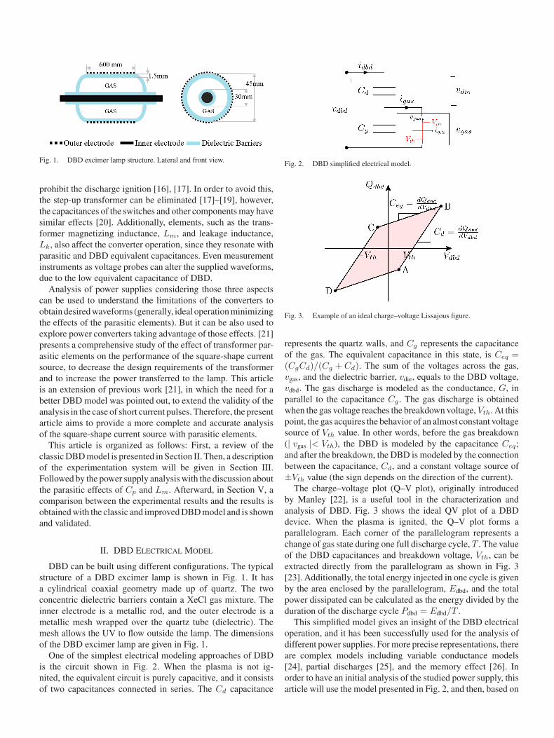
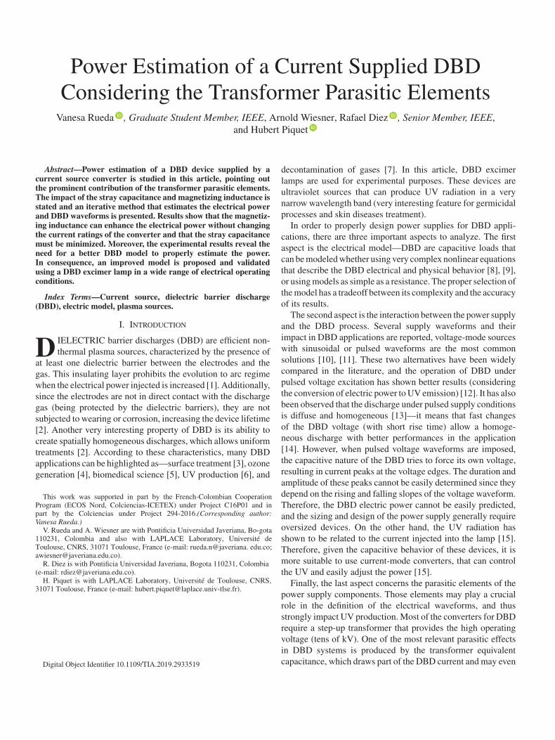
Fig. 1. DBD excimer lamp structure. Lateral and front view.
prohibit the discharge ignition [16], [17]. In order to avoid this,the step-up transformer can be eliminated [17]–[19], however,the capacitances of the switches and other components may havesimilar effects [20]. Additionally, elements, such as the trans-former magnetizing inductance, Lm, and leakage inductance,Lk, also affect the converter operation, since they resonate withparasitic and DBD equivalent capacitances. Even measurementinstruments as voltage probes can alter the supplied waveforms,due to the low equivalent capacitance of DBD.
Analysis of power supplies considering those three aspectscan be used to understand the limitations of the converters toobtain desired waveforms (generally, ideal operation minimizingthe effects of the parasitic elements). But it can be also used toexplore power converters taking advantage of those effects. [21]presents a comprehensive study of the effect of transformer par-asitic elements on the performance of the square-shape currentsource, to decrease the design requirements of the transformerand to increase the power transferred to the lamp. This articleis an extension of previous work [21], in which the need for abetter DBD model was pointed out, to extend the validity of theanalysis in the case of short current pulses. Therefore, the presentarticle aims to provide a more complete and accurate analysisof the square-shape current source with parasitic elements.
This article is organized as follows: First, a review of theclassic DBD model is presented in Section II. Then, a descriptionof the experimentation system will be given in Section III.Followed by the power supply analysis with the discussion aboutthe parasitic effects of Cp and Lm. Afterward, in Section V, acomparison between the experimental results and the results isobtained with the classic and improved DBD model and is shownand validated.
II. DBD ELECTRICAL MODEL
DBD can be built using different configurations. The typicalstructure of a DBD excimer lamp is shown in Fig. 1. It hasa cylindrical coaxial geometry made up of quartz. The twoconcentric dielectric barriers contain a XeCl gas mixture. Theinner electrode is a metallic rod, and the outer electrode is ametallic mesh wrapped over the quartz tube (dielectric). Themesh allows the UV to flow outside the lamp. The dimensionsof the DBD excimer lamp are given in Fig. 1.
One of the simplest electrical modeling approaches of DBDis the circuit shown in Fig. 2. When the plasma is not ig-nited, the equivalent circuit is purely capacitive, and it consistsof two capacitances connected in series. The Cd capacitance
Fig. 2. DBD simplified electrical model.
Fig. 3. Example of an ideal charge–voltage Lissajous figure.
represents the quartz walls, and Cg represents the capacitanceof the gas. The equivalent capacitance in this state, is Ceq =(CgCd)/(Cg + Cd). The sum of the voltages across the gas,vgas, and the dielectric barrier, vdie, equals to the DBD voltage,vdbd. The gas discharge is modeled as the conductance, G, inparallel to the capacitance Cg . The gas discharge is obtainedwhen the gas voltage reaches the breakdown voltage,Vth. At thispoint, the gas acquires the behavior of an almost constant voltagesource of Vth value. In other words, before the gas breakdown(| vgas |< Vth), the DBD is modeled by the capacitance Ceq;and after the breakdown, the DBD is modeled by the connectionbetween the capacitance, Cd, and a constant voltage source of±Vth value (the sign depends on the direction of the current).
The charge–voltage plot (Q–V plot), originally introducedby Manley [22], is a useful tool in the characterization andanalysis of DBD. Fig. 3 shows the ideal QV plot of a DBDdevice. When the plasma is ignited, the Q–V plot forms aparallelogram. Each corner of the parallelogram represents achange of gas state during one full discharge cycle, T . The valueof the DBD capacitances and breakdown voltage, Vth, can beextracted directly from the parallelogram as shown in Fig. 3[23]. Additionally, the total energy injected in one cycle is givenby the area enclosed by the parallelogram, Edbd, and the totalpower dissipated can be calculated as the energy divided by theduration of the discharge cycle Pdbd = Edbd/T .
This simplified model gives an insight of the DBD electricaloperation, and it has been successfully used for the analysis ofdifferent power supplies. For more precise representations, thereare complex models including variable conductance models[24], partial discharges [25], and the memory effect [26]. Inorder to have an initial analysis of the studied power supply, thisarticle will use the model presented in Fig. 2, and then, based on
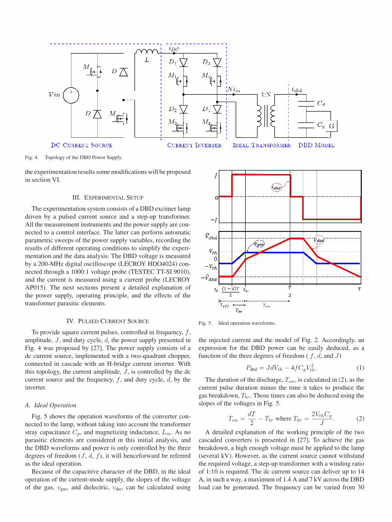
Fig. 4. Topology of the DBD Power Supply.
the experimentation results some modifications will be proposedin section VI.
III. EXPERIMENTAL SETUP
The experimentation system consists of a DBD excimer lampdriven by a pulsed current source and a step-up transformer.All the measurement instruments and the power supply are con-nected to a control interface. The latter can perform automaticparametric sweeps of the power supply variables, recording theresults of different operating conditions to simplify the experi-mentation and the data analysis. The DBD voltage is measuredby a 200-MHz digital oscilloscope (LECROY HDO4024) con-nected through a 1000:1 voltage probe (TESTEC TT-SI 9010),and the current is measured using a current probe (LECROYAP015). The next sections present a detailed explanation ofthe power supply, operating principle, and the effects of thetransformer parasitic elements.
IV. PULSED CURRENT SOURCE
To provide square current pulses, controlled in frequency, f ,amplitude, J , and duty cycle, d, the power supply presented inFig. 4 was proposed by [27]. The power supply consists of adc current source, implemented with a two-quadrant chopper,connected in cascade with an H-bridge current inverter. Withthis topology, the current amplitude, J , is controlled by the dccurrent source and the frequency, f , and duty cycle, d, by theinverter.
A. Ideal Operation
Fig. 5 shows the operation waveforms of the converter con-nected to the lamp, without taking into account the transformerstray capacitance Cp, and magnetizing inductance, Lm. As noparasitic elements are considered in this initial analysis, andthe DBD waveforms and power is only controlled by the threedegrees of freedom (J , d, f ), it will henceforward be referredas the ideal operation.
Because of the capacitive character of the DBD, in the idealoperation of the current-mode supply, the slopes of the voltageof the gas, vgas, and dielectric, vdie, can be calculated using
Fig. 5. Ideal operation waveforms.
the injected current and the model of Fig. 2. Accordingly, anexpression for the DBD power can be easily deduced, as afunction of the three degrees of freedom ( f , d, and J)
Pdbd = JdVth − 4fCgV2th. (1)
The duration of the discharge, Ton, is calculated in (2), as thecurrent pulse duration minus the time it takes to produce thegas breakdown, Tbr. Those times can also be deduced using theslopes of the voltages in Fig. 5.
Ton =dT
2− Tbr where Tbr =
2VthCg
J. (2)
A detailed explanation of the working principle of the twocascaded converters is presented in [27]. To achieve the gasbreakdown, a high enough voltage must be applied to the lamp(several kV). However, as the current source cannot withstandthe required voltage, a step-up transformer with a winding ratioof 1:10 is required. The dc current source can deliver up to 14A, in such a way, a maximum of 1.4 A and 7 kV across the DBDload can be generated. The frequency can be varied from 30
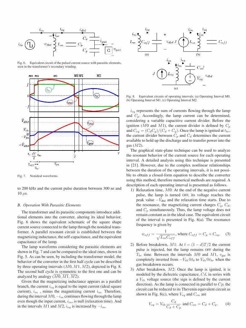
Fig. 6. Equivalent circuit of the pulsed current source with parasitic elements,seen in the transformer’s secondary winding.
Fig. 7. Nonideal waveforms.
to 200 kHz and the current pulse duration between 300 ns and10 µs.
B. Operation With Parasitic Elements
The transformer and its parasitic components introduce addi-tional elements into the converter, altering its ideal behavior.Fig. 6 shows the equivalent schematic of the square shapecurrent source connected to the lamp through the nonideal trans-former. A parallel resonant circuit is established between themagnetizing inductance, the self-capacitance, and the equivalentcapacitance of the lamp.
The lamp waveforms considering the parasitic elements areshown in Fig. 7 and can be compared to the ideal ones, shown inFig. 5. As can be seen, by including the transformer model, thebehavior of the converter in the first half cycle can be describedby three operating intervals (M0,M1,M2), depicted in Fig. 8.The second half cycle is symmetric to the first one and can beanalyzed by analogy (M0,M1,M2).
Given that the magnetizing inductance appears as a parallelbranch, the current ieq is equal to the input current (ideal squarecurrent), iin , minus the magnetizing current im. Therefore,during the intervalM0,−im continues flowing through the lampeven though the input current, iin, is null (relaxation time). Andin the intervals M1 and M2, ieq is increased by −im.
Fig. 8. Equivalent circuits of operating intervals. (a) Operating Interval M0.(b) Operating Interval M1. (c) Operating Interval M2.
ieq represents the sum of currents flowing through the lampand Cp. Accordingly, the lamp current can be determined,considering a variable capacitive current divider. Before theignition (M0 and M1), the current divider is defined by Cp
and Ceq = (CdCg)/(Cd + Cg). Once the lamp is ignited at tbr,the current divider between Cp and Cd determines the currentavailable to hold up the discharge and to transfer power into thegas (M2).
The graphical state-plane technique can be used to analyzethe resonant behavior of the current source for each operatinginterval. A detailed analysis using this technique is presentedin [21]. However, due to the complex nonlinear relationshipsbetween the duration of the operating intervals, it is not possi-ble to obtain a closed-form equation to describe the converterusing this method, therefore numerical methods are required. Adescription of each operating interval is presented as follows.
1) Relaxation time, M0: At the end of the negative currentpulse, the lamp is turned OFF, its voltage reaches thepeak value ˆ−Vdbd and the relaxation time starts. Due tothe resonance, the magnetizing current charges Cg , Cd,and Cp simultaneously. Thus, the lamp voltage does notremain constant as in the ideal case. The equivalent circuitof the interval is presented in Fig. 8(a). The resonancefrequency is given by
woff =1
√LmCoff
, where Coff = Cp + Ceq. (3)
2) Before breakdown, M1: At t = (1 − d)T/2 the currentpulse is injected, but the lamp remains OFF during theTbr time. Between the intervals M0 and M1, vgas iscompletely inverted from −Vth@t0 to Vth@tbr when thegas breakdown occurs.
3) After breakdown, M2: Once the lamp is ignited, it ismodeled by the dielectric capacitance, Cd, in series witha Vth voltage source (the sign is defined by the currentdirection). As the lamp is connected in parallel to Cp, thecircuit can be reduced to its Thevenin equivalent circuit asshown in Fig. 8(c), where Veq and Con are
Veq = VthCd
Cd + Cpand Con = Cd + Cp. (4)
Due to the change of the equivalent capacitance of thelamp, the resonance frequency must be redefined aswon =1/√LmCon. This operating interval finishes when the
current pulse ends, it means that Tbr + Ton = dT2 .
V. EFFECTS OF THE ELEMENTS OF THE TRANSFORMER
Numerical analysis is proposed to find the solution of theoutput waveforms under the effects of the parasitic elements.An iterative method to successively find better approximationsof the DBD waveforms is proposed. This method starts with theideal DBD voltage waveform (without the transformer effects),vdbd, to calculate the magnetizing current of the first iteration inthe following:
im,n =1L
∫vdbd,n−1dt (5)
where n is the iteration number.Once the magnetizing current has been calculated, the DBD
current can be deduced using current divider formed betweenthe parasitic capacitance and the DBD
idbd,n =
⎧⎪⎪⎪⎨
⎪⎪⎪⎩
(iin − im,n)Ceq
Ceq + Cpbefore breakdown
(iin − im,n)Cd
Cd + Cpafter breakdown
. (6)
Then, idbd,n is used to solve the equations of the DBD model(8) and (9), and thus, to find the DBD voltage and DBD power
vgas,n =
⎧⎨
⎩
1Cg
∫idbd,ndt before breakdown
±Vth after breakdown(7)
vdie,n =1Cd
∫idbd,ndt (8)
vdbd,n = vgas,n + vdie,n. (9)
These operations are recursively executed until the calcula-tion of the DBD power converges. The numerical analysis isimplemented in Matlab in order to achieve a fast estimation ofthe converter behavior [28]. Compared to simulation, with thismethod one can perform sweeps of supply and lamp parameters,using only a few iterations for the convergence. With a circuitsolver, the simulation time required to get the steady stateis much higher than the iterations used in our method. Theresulting waveforms are compared with experimental results inthe following sections.
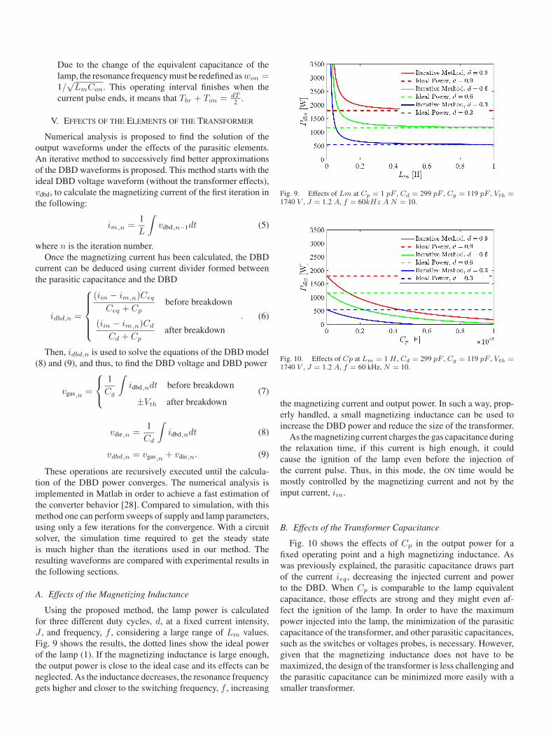
A. Effects of the Magnetizing Inductance
Using the proposed method, the lamp power is calculatedfor three different duty cycles, d, at a fixed current intensity,J , and frequency, f , considering a large range of Lm values.Fig. 9 shows the results, the dotted lines show the ideal powerof the lamp (1). If the magnetizing inductance is large enough,the output power is close to the ideal case and its effects can beneglected. As the inductance decreases, the resonance frequencygets higher and closer to the switching frequency, f , increasing
Fig. 9. Effects of Lm at Cp = 1 pF , Cd = 299 pF , Cg = 119 pF , Vth =1740 V , J = 1.2 A, f = 60kHz A N = 10.
Fig. 10. Effects of Cp at Lm = 1 H , Cd = 299 pF , Cg = 119 pF , Vth =1740 V , J = 1.2 A, f = 60 kHz, N = 10.
the magnetizing current and output power. In such a way, prop-erly handled, a small magnetizing inductance can be used toincrease the DBD power and reduce the size of the transformer.
As the magnetizing current charges the gas capacitance duringthe relaxation time, if this current is high enough, it couldcause the ignition of the lamp even before the injection ofthe current pulse. Thus, in this mode, the ON time would bemostly controlled by the magnetizing current and not by theinput current, iin.
B. Effects of the Transformer Capacitance
Fig. 10 shows the effects of Cp in the output power for afixed operating point and a high magnetizing inductance. Aswas previously explained, the parasitic capacitance draws partof the current ieq , decreasing the injected current and powerto the DBD. When Cp is comparable to the lamp equivalentcapacitance, those effects are strong and they might even af-fect the ignition of the lamp. In order to have the maximumpower injected into the lamp, the minimization of the parasiticcapacitance of the transformer, and other parasitic capacitances,such as the switches or voltages probes, is necessary. However,given that the magnetizing inductance does not have to bemaximized, the design of the transformer is less challenging andthe parasitic capacitance can be minimized more easily with asmaller transformer.
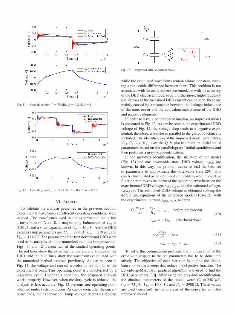
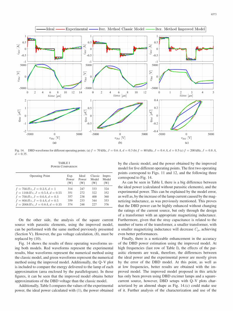
Fig. 11. Operating point f = 70 kHz, J = 0.2 A, d = 1.
Fig. 12. Operating point f = 110 kHz, J = 0.4 A, d = 0.55.
VI. RESULTS
To validate the analysis presented in the previous section,experimental waveforms at different operating conditions werestudied. The transformer used in the experimental setup hasa turns ratio of N = 10, a magnetizing inductance of Lm =0.08 H , and a stray capacitance of Cp = 16 pF . And the DBDexcimer lamp parameters are: Cd = 299 pF , Cg = 119 pF , andVth = 1740 V . The parameter of the transformer and DBD wereused in the analysis of all the numerical methods here presented.Figs. 11 and 12 present two of the studied operating points.The red lines show the experimental current and voltage of theDBD, and the blue lines show the waveforms calculated withthe numerical method exposed previously. As can be seen inFig. 11, the voltage and current waveforms are similar to theexperimental ones. This operating point is characterized by ahigh duty cycle. Under this condition, the proposed analysisworks properly. However, when the duty cycle is reduced, theanalysis is less accurate. Fig. 12 presents one operating pointobtained under such conditions. As can be seen, after the currentpulse ends, the experimental lamp voltage decreases rapidly,
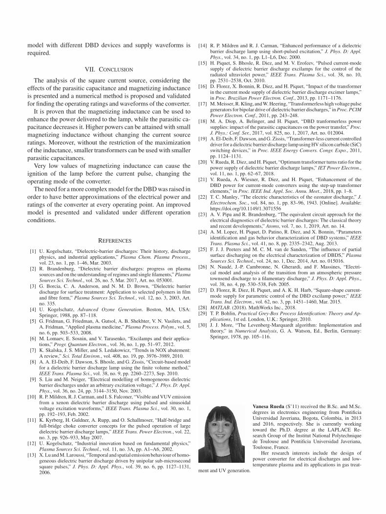
Fig. 13. Improved DBD electrical model.
while the calculated waveforms remain almost constant, creat-ing a noticeable difference between them. This problem is notassociated with the analysis here presented, but with the accuracyof the DBD electrical model used. Furthermore, high-frequencyoscillations in the measured DBD current can be seen, these aremainly caused by a resonance between the leakage inductanceof the transformer and the equivalent capacitance of the DBDand parasitic elements.
In order to have a better approximation, an improved modelis presented in Fig. 13. As can be seen in the experimental DBDvoltage of Fig. 12, the voltage drop tends to a negative expo-nential, therefore, a resistor in parallel to the gas conductance isincluded. The identification of the improved model parameters,[Cd, Cg, Vth, Rg], uses the Q–V plot to obtain an initial set ofparameters based on the parallelogram (initial conditions) andthen performs a grey-box identification.
In the grey-box identification, the structure of the model(Fig. 13) and one observable state (DBD voltage, vdbd) areknown. In this way, the problem seeks to find the best setof parameters to approximate the observable state [29]. Thiscan be formulated as an optimization problem which objectivefunction minimizes the norm of the quadratic error between theexperimental DBD voltage, vdbdEXP , and the estimated voltage,vdbdEST . The estimated DBD voltage is obtained solving thedifferential equations of the improved model (10)–(12), withthe experimental current, idbdEXP , as input
Cgdvgas
dt+
vgas
Rg= idbd, before breakdown
vgas = ±Vth, after breakdown
(10)
Cddvdie
dt= idbd (11)
vdbd = vgas + vdie. (12)
To solve this optimization problem, the minimization of theerror with respect to the set parameters has to be done iter-atively. The objective of each iteration is to find the distur-bance to the parameters that reduce the objective function. TheLevenberg–Marquardt gradient algorithm was used to find theDBD parameters [30]. After using the grey-box identification,the obtained parameters of the model were: Cg = 248 pF ,Cd = 73 pF , Vth = 1600 V , and Rg = 2900 Ω. These valuesare used henceforth in the analysis of the converter with theimproved model.
6573
Fig. 14. DBD waveforms for different operating points. (a) f = 70 kHz, J = 0.6 A, d = 0.3 (b) f = 80 kHz, J = 0.4 A, d = 0.5 (c) f = 200 kHz, J = 0.8 A,d = 0.35.
TABLE IPOWER COMPARISON
On the other side, the analysis of the square currentsource with parasitic elements, using the improved model,can be performed with the same method previously presented(Section V). However, the gas voltage calculation, (8), must bereplaced by (10).
Fig. 14 shows the results of three operating waveforms us-ing both models. Red waveforms represent the experimentalresults, blue waveforms represent the numerical method usingthe classic model, and green waveforms represent the numericalmethod using the improved model. Additionally, the Q–V plotis included to compare the energy delivered to the lamp of eachapproximation (area enclosed by the parallelogram). In thosefigures, it can be seen that the improved model obtains betterapproximations of the DBD voltage than the classic model.
Additionally, Table I compares the values of the experimentalpower, the ideal power calculated with (1), the power obtained
by the classic model, and the power obtained by the improvedmodel for five different operating points. The first two operatingpoints correspond to Figs. 11 and 12, and the following threecorrespond to Fig. 14.
As can be seen in Table I, there is a big difference betweenthe ideal power (calculated without parasitic elements), and theexperimental power. This can be explained by the model error,as well as, by the increase of the lamp current caused by the mag-netizing inductance, as was previously mentioned. This provesthat the DBD power can be highly enhanced without changingthe ratings of the current source, but only through the designof a transformer with an appropriate magnetizing inductance.Furthermore, given that the stray capacitance is related to thenumber of turns of the transformer, a smaller transformer, witha smaller magnetizing inductance will decrease Cp, achievingeven better performances.
Finally, there is a noticeable enhancement in the accuracyof the DBD power estimation using the improved model. Athigh frequencies (last row of Table I), the effects of the par-asitic elements are weak, therefore, the differences betweenthe ideal power and the experimental power are mostly givenby the error of the DBD model. At this point, as well asat low frequencies, better results are obtained with the im-proved model. The improved model proposed in this articlehas only been proven using DBD excimer lamps and a square-current source, however, DBD setups with Q–V plots char-acterized by an almond shape as Fig. 14.(c) could make useof it. Further analysis of the characterization and use of the
model with different DBD devices and supply waveforms isrequired.
VII. CONCLUSION
The analysis of the square current source, considering theeffects of the parasitic capacitance and magnetizing inductanceis presented and a numerical method is proposed and validatedfor finding the operating ratings and waveforms of the converter.
It is proven that the magnetizing inductance can be used toenhance the power delivered to the lamp, while the parasitic ca-pacitance decreases it. Higher powers can be attained with smallmagnetizing inductance without changing the current sourceratings. Moreover, without the restriction of the maximizationof the inductance, smaller transformers can be used with smallerparasitic capacitances.
Very low values of magnetizing inductance can cause theignition of the lamp before the current pulse, changing theoperating mode of the converter.
The need for a more complex model for the DBD was raised inorder to have better approximations of the electrical power andratings of the converter at every operating point. An improvedmodel is presented and validated under different operationconditions.
REFERENCES
[1] U. Kogelschatz, “Dielectric-barrier discharges: Their history, dischargephysics, and industrial applications,” Plasma Chem. Plasma Process.,vol. 23, no. 1, pp. 1–46, Mar. 2003.
[2] R. Brandenburg, “Dielectric barrier discharges: progress on plasmasources and on the understanding of regimes and single filaments,” PlasmaSources Sci. Technol., vol. 26, no. 5, Mar. 2017, Art. no. 053001.
[3] G. Borcia, C. A. Anderson, and N. M. D. Brown, “Dielectric barrierdischarge for surface treatment: Application to selected polymers in filmand fibre form,” Plasma Sources Sci. Technol., vol. 12, no. 3, 2003, Art.no. 335.
[4] U. Kogelschatz, Advanced Ozone Generation. Boston, MA, USA:Springer, 1988, pp. 87–118.
[5] G. Fridman, G. Friedman, A. Gutsol, A. B. Shekhter, V. N. Vasilets, andA. Fridman, “Applied plasma medicine,” Plasma Process. Polym., vol. 5,no. 6, pp. 503–533, 2008.
[6] M. Lomaev, E. Sosnin, and V. Tarasenko, “Excilamps and their applica-tions,” Progr. Quantum Electron., vol. 36, no. 1, pp. 51–97, 2012.
[7] K. Skalska, J. S. Miller, and S. Ledakowicz, “Trends in NOX abatement:A review,” Sci. Total Environ., vol. 408, no. 19, pp. 3976–3989, 2010.
[8] A. A. El-Deib, F. Dawson, S. Bhosle, and G. Zissis, “Circuit-based modelfor a dielectric barrier discharge lamp using the finite volume method,”IEEE Trans. Plasma Sci., vol. 38, no. 9, pp. 2260–2273, Sep. 2010.
[9] S. Liu and M. Neiger, “Electrical modelling of homogeneous dielectricbarrier discharges under an arbitrary excitation voltage,” J. Phys. D: Appl.Phys., vol. 36, no. 24, pp. 3144–3150, Nov. 2003.
[10] R. P. Mildren, R. J. Carman, and I. S. Falconer, “Visible and VUV emissionfrom a xenon dielectric barrier discharge using pulsed and sinusoidalvoltage excitation waveforms,” IEEE Trans. Plasma Sci., vol. 30, no. 1,pp. 192–193, Feb. 2002.
[11] K. Kyrberg, H. Guldner, A. Rupp, and O. Schallmoser, “Half-bridge andfull-bridge choke converter concepts for the pulsed operation of largedielectric barrier discharge lamps,” IEEE Trans. Power Electron., vol. 22,no. 3, pp. 926–933, May 2007.
[12] U. Kogelschatz, “Industrial innovation based on fundamental physics,”Plasma Sources Sci. Technol., vol. 11, no. 3A, pp. A1–A6, 2002.
[13] X. Lu and M. Laroussi, “Temporal and spatial emission behaviour of homo-geneous dielectric barrier discharge driven by unipolar sub-microsecondsquare pulses,” J. Phys. D: Appl. Phys., vol. 39, no. 6, pp. 1127–1131,2006.
[14] R. P. Mildren and R. J. Carman, “Enhanced performance of a dielectricbarrier discharge lamp using short-pulsed excitation,” J. Phys. D: Appl.Phys., vol. 34, no. 1, pp. L1–L6, Dec. 2000.
[15] H. Piquet, S. Bhosle, R. Diez, and M. V. Erofeev, “Pulsed current-modesupply of dielectric barrier discharge excilamps for the control of theradiated ultraviolet power,” IEEE Trans. Plasma Sci., vol. 38, no. 10,pp. 2531–2538, Oct. 2010.
[16] D. Florez, X. Bonnin, R. Diez, and H. Piquet, “Impact of the transformerin the current mode supply of dielectric barrier discharge excimer lamps,”in Proc. Brazilian Power Electron. Conf., 2013, pp. 1171–1176.
[17] M. Meisser, R. Kling, and W. Heering, “Transformerless high voltage pulsegenerators for bipolar drive of dielectric barrier discharges,” in Proc. PCIMPower Electron. Conf., 2011, pp. 243–248.
[18] M. A. Diop, A. Belinger, and H. Piquet, “DBD tranformerless powersupplies: impact of the parasitic capacitances on the power transfer,” Proc.J. Phys.: Conf. Ser., 2017, vol. 825, no. 1, 2017, Art. no. 012004.
[19] A. El-Deib, F. Dawson, and G. Zissis, “Transformer-less current controlleddriver for a dielectric barrier discharge lamp using HV silicon carbide (SiC)switching devices,” in Proc. IEEE Energy Convers. Congr. Expo., 2011,pp. 1124–1131.
[20] V. Rueda, R. Diez, and H. Piquet, “Optimum transformer turns ratio for thepower supply of dielectric barrier discharge lamps,” IET Power Electron.,vol. 11, no. 1, pp. 62–67, 2018.
[21] V. Rueda, A. Wiesner, R. Diez, and H. Piquet, “Enhancement of theDBD power for current-mode converters using the step-up transformerelements,” in Proc. IEEE Ind. Appl. Soc. Annu. Meet., 2018, pp. 1–8.
[22] T. C. Manley, “The electric characteristics of the ozonator discharge,” J.Electrochem. Soc., vol. 84, no. 1, pp. 83–96, 1943. [Online]. Available:https://doi.org/10.1149/1.3071556
[23] A. V. Pipa and R. Brandenburg, “The equivalent circuit approach for theelectrical diagnostics of dielectric barrier discharges: The classical theoryand recent developments,” Atoms, vol. 7, no. 1, 2019, Art. no. 14.
[24] A. M. Lopez, H. Piquet, D. Patino, R. Diez, and X. Bonnin, “Parametersidentification and gas behavior characterization of DBD systems,” IEEETrans. Plasma Sci., vol. 41, no. 8, pp. 2335–2342, Aug. 2013.
[25] F. J. J. Peeters and M. C. M. van de Sanden, “The influence of partialsurface discharging on the electrical characterization of DBDS,” PlasmaSources Sci. Technol., vol. 24, no. 1, Dec. 2014, Art. no. 015016.
[26] N. Naudé, J.-P. Cambronne, N. Gherardi, and F. Massines, “Electri-cal model and analysis of the transition from an atmospheric pressuretownsend discharge to a filamentary discharge,” J. Phys. D: Appl. Phys.,vol. 38, no. 4, pp. 530–538, Feb. 2005.
[27] D. Florez, R. Diez, H. Piquet, and A. K. H. Harb, “Square-shape current-mode supply for parametric control of the DBD excilamp power,” IEEETrans. Ind. Electron., vol. 62, no. 3, pp. 1451–1460, Mar. 2015.
[28] MATLAB. (2018). MathWorks Inc., 2018.[29] T. P. Bohlin, Practical Grey-Box Process Identification: Theory and Ap-
plications, 1st ed. London, U.K.: Springer, 2010.[30] J. J. More, “The Levenberg-Marquardt algorithm: Implementation and
theory,” in Numerical Analysis, G. A. Watson, Ed., Berlin, Germany:Springer, 1978, pp. 105–116.
Vanesa Rueda (S’11) received the B.Sc. and M.Sc.degrees in electronics engineering from PontificiaUniversidad Javeriana, Bogota, Colombia, in 2013and 2016, respectively. She is currently workingtoward the Ph.D. degree at the LAPLACE Re-search Group of the Institut National Polytechniquede Toulouse and Pontificia Universidad Javeriana,Toulouse, France.
Her research interests include the design ofpower converter for electrical discharges and low-temperature plasma and its applications in gas treat-
ment and UV generation.
Arnold Wiesner received the B.S. and M.Sc. de-grees in electronics engineering from Pontificia Uni-versidad Javeriana, Bogota, Colombia, in 2012 and2013, respectively. He is currently working toward thePh.D. degree at the Institut National Polytechnique deToulouse, Toulouse, France.
He is currently an Assistant Professor with the De-partment of Electronics, Universidad Santo Tomas,Bogota, Colombia. His current research interests in-clude power converters for dielectric barrier dis-charges and renewable energy systems.
Rafael Dez (M’10–SM’15) received the B.Sc. de-gree in electronics engineering from Pontificia Uni-versidad Javeriana, Bogota, Colombia, in 2001, theM.Sc. degree in 2005 from Universit Paul Sabatier,Toulouse, France, and the Ph.D. degree in 2008from the Institut National Polytechnique de Toulouse,Toulouse, France.
He is currently an Associate Professor with theDepartment of Electronics Engineering, PontificiaUniversidad Javeriana, Bogota, Colombia. His cur-rent research interests include the design of power
converters for electric discharges.
Hubert Piquet was born in Arras, France, in 1960. Hegraduated in applied physics from the Ecole NormaleSuprieure de Cachan, Cachan, France in 1984 andreceived the Ph.D. degree in electrical engineeringfrom the Institut National Polytechnique de Toulouse,Toulouse, France, in 1990.
He is currently a Professor with ToulouseINP/ENSEEIHT Ing. School. He teaches power elec-tronics and systemic approach in electrical engineer-ing. His current research interests include plasmaapplications and design of aircraft electrical networks
and the investigation takes place in the LAPLACE laboratory, Toulouse, France.

![DBD plasma microbubble reactor for pre-treatment of … · DBD plasma microbubble reactor for pre-treatment of lignocellulosic biomass [poster] ... DBD plasma microbubble reactor](https://img.pdfslide.us/doc/110x75/5e4523a0e85b14090f08d100/dbd-plasma-microbubble-reactor-for-pre-treatment-of-dbd-plasma-microbubble-reactor.jpg)