Embed Size (px)
Citation preview
598 IEEE TRANSACTIONS ON ELECTRON DEVICES, VOL. 61, NO. 2, FEBRUARY 2014
Polycrystalline Silicon Nanowires SynthesisCompatible With CMOS Technology for
Integrated Gas Sensing ApplicationsRegis Rogel, Emmanuel Jacques, Laurent Pichon, and Anne Claire Salaun
Abstract— Polysilicon nanowires are synthesized following aclassical top–down approach using conventional UV lithog-raphy technique fully compatible with the existing siliconcomplementary metal–oxide–semiconductor technology. N- andP-type in situ doping of these nanowires is controlled over alarge range of doping levels and the electrical properties ofthese nanowires are analyzed. The results show that resistivitydependence with the doping level is both related to the nanowiresize-dependent structural quality and doping specie. Chargedgas species (ammonia) sensitivity of these nanowires has alsobeen studied. In addition, the feasibility of N- and P-channelpolysilicon nanowire transistors is demonstrated.
Index Terms— In situ doping, LPCVD, nanowires, polysilicon,thin-film transistor (TFT).
I. INTRODUCTION
SEMICONDUCTING nanowires are currently attractingmuch attention as promising components for future nano-
electronic devices, such as nanowire field-effect transistors [1],photonic and optoelectronic devices [2], and more particularlyas chemical or biological sensors [3]–[5]. The needs of a fastand precise detection of early disease symptoms, as well asthe need of environment safety, become now the main leitmo-tiv of the societal development. The incorporation of semi-conducting nanowires into chemical and biological sensorsapplications receives a great interest. As their surface can besensitive to charged species combined with their high surface-to-volume ratio, semiconducting nanowires are the subjectof intense research activities for high-sensitivity chemicalsensor fabrication. In particular, for silicon nanowires (SiNWs)based electronic devices, the highly sensitive detection basedon SiNWs enables a change in current when, after surfacefunctionalization, the analytical (charged) molecules bind tospecific recognition molecule at the SiNWs surface. In thisway, many studies reported on biological sensors for DNAhybridation [4], and chemical [6] and gas detection [7].
Manuscript received July 25, 2012; revised December 2, 2013; acceptedDecember 13, 2013. Date of current version January 20, 2014. This workwas supported by the Agence Nationale de la Recherche under Project SenaANR-09JCJC-0072-01. The review of this paper was arranged by EditorA. M. Ionescu.
The authors are with the Institut d’Electronique et de Télécommunicationsde Rennes, Université de Rennes 1, Rennes cedex 35042, France (e-mail:[email protected]; [email protected]; [email protected]; [email protected]).
Color versions of one or more of the figures in this paper are availableonline at http://ieeexplore.ieee.org.
Digital Object Identifier 10.1109/TED.2013.2295511
SiNWs can be prepared by one of two approaches, topdown and bottom up. In a bottom-up strategy, the individ-ual base elements (atoms, molecules, etc.) of the systemare linked together to form larger subsystems. Most of thedeveloped synthesis methods are layer-by-layer self assembly[8], vapor–liquid–solid and solid–liquid–solid growth tech-niques [9], [10], and using matrix template [11]. The maindrawbacks of these synthesis methods for a 3-D integrationare the difficulty in control of size and positioning of thenanowires. In this case, nanowires need to be selectivelycollected and manipulated to be assembled in a planar layout.The top-down approach starts from bulk materials and scalesdown the patterned areas. In this way, several advancednanopatterning techniques were developed, such as e-beam[12], atomic force microscopy [13], [14], deep UV [15], andnanoimprint lithographies [16], [17], to obtain SiNWs. Themain drawbacks of these advanced lithographic tools withnanometer-size resolution rest on the high cost generated, andmore generally the low throughput capability unsuitable withmass production. Because SiNWs synthesis can be compatiblewith the established silicon technology, SiNWs-based sensorintegration will allow a lower manufacturing cost, in additionto the advantageous electronic features of embedded detectionand signal processing in silicon technology. The intrinsicreliability of the well-known semiconductor complementarymetal–oxide–semiconductor (CMOS) process also guaranteesreproducible and reliable performances. Recently, previousworks demonstrated the CMOS compatibility of SiNWs top-down fabrication. Some of them [18] reported on SiNWselectronic building blocks, with nanowires fabricated fromsilicon bulk substrate, and then collected to another (plastic)substrate. Buddharaju et al. [19] and Wessely et al. [20] usede-beam lithography techniques for SiNWs fabrication usingcostly silicon-on-insulator substrates.
In addition, a high-reliable doping control at nanoscalestill remains a challenge for the development of nanoscaledevice integrated in electronic, sensing, and photonic, systems.The ability to predict and control electronic doping level ofSiNWs, using the knowledge obtained from the planar silicontechnology, is a key feature for nanoscale device applications.In other words, high and uniform doping control is requiredfor a precise control of electrical properties of SiNWs-baseddevices. In this paper, we present a direct patterning techniqueof in situ doped SiNWs planar arrays by conventional opticallithography, compatible with the existing planar CMOS silicon
0018-9383 © 2014 IEEE. Personal use is permitted, but republication/redistribution requires IEEE permission.See http://www.ieee.org/publications_standards/publications/rights/index.html for more information.
ROGEL et al.: POLYCRYSTALLINE SINWs SYNTHESIS COMPATIBLE WITH CMOS TECHNOLOGY 599
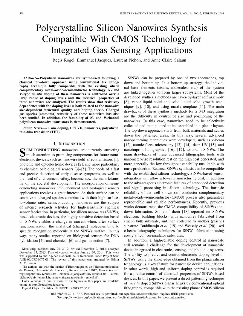
Fig. 1. (a) Fabrication of polycrystalline SiNWs by the sidewall spacerformation technique. (b) Polycrystalline SiNWs-based resistor for electricalcharacterization.
technology. Such SiNWS are promising active building blocksfor gas (ammonia) sensors and electronics.
II. EXPERIMENTS
The key fabrication steps of the polycrystalline SiNWs areshown in Fig. 1(a). At first, a dielectric film A is deposited andpatterned into islands by conventional UV lithography. Then, apolycrystalline silicon layer is deposited by LPCVD technique.Accurate control of the polycrystalline silicon layer reactiveion etching (RIE) rate leads to the formation of nanometric sizesidewall spacers that can be used as nanowires. The feasibilityof these polyscristalline SiNWs with curvature radius as low as50 nm was previously demonstrated [21]. This method allowsthe fabrication of parallel SiNWs network.
Phosphorus (or boron) in situ doped polycrystalline sili-con layers used for such nanowires were deposited by thethermal decomposition of a mixture of pure silane, SiH4,and phosphine, PH3, (or diborane, B2H6). The in situ dopinglevel is controlled by adjusting the PH3/SiH4 (or B2H6/SiH4)mole ratio varying from zero for undoped films to 4 × 10⁻⁴
(or 5 × 10⁻⁴) for heavily doped films. Silicon films weredeposited in an amorphous state at 550 °C and 90 Pa, and thencrystallized by a thermal annealing in vacuum at 600 °C during12 h. The corresponding incorporated phosphorus (boron)atoms concentrations, CP (CB), previously determined fromsecondary ions mass spectroscopy (SIMS) analysis, varies
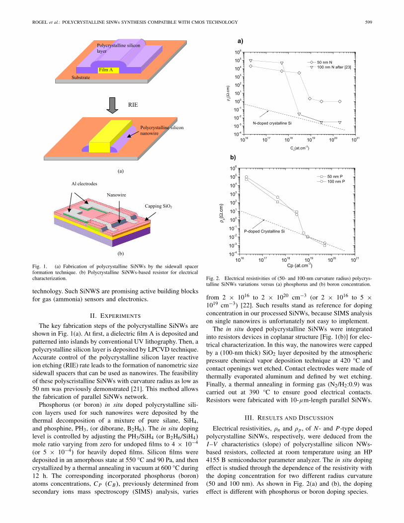
Fig. 2. Electrical resistivities of (50- and 100-nm curvature radius) polycrys-talline SiNWs variations versus (a) phosphorus and (b) boron concentration.
from 2 × 10¹⁶ to 2 × 1020 cm−3 (or 2 × 10¹⁶ to 5 ×1019 cm−3) [22]. Such results stand as reference for dopingconcentration in our processed SiNWs, because SIMS analysison single nanowires is unfortunately not easy to implement.
The in situ doped polycrystalline SiNWs were integratedinto resistors devices in coplanar structure [Fig. 1(b)] for elec-trical characterization. In this way, the nanowires were cappedby a (100-nm thick) SiO2 layer deposited by the atmosphericpressure chemical vapor deposition technique at 420 °C andcontact openings wet etched. Contact electrodes were made ofthermally evaporated aluminum and defined by wet etching.Finally, a thermal annealing in forming gas (N2/H2:0.9) wascarried out at 390 °C to ensure good electrical contacts.Resistors were fabricated with 10-μm-length parallel SiNWs.
III. RESULTS AND DISCUSSION
Electrical resistivities, ρn and ρp , of N- and P-type dopedpolycrystalline SiNWs, respectively, were deduced from theI–V characteristics (slope) of polycrystalline silicon NWs-based resistors, collected at room temperature using an HP4155 B semiconductor parameter analyzer. The in situ dopingeffect is studied through the dependence of the resistivity withthe doping concentration for two different radius curvature(50 and 100 nm). As shown in Fig. 2(a) and (b), the dopingeffect is different with phosphorus or boron doping species.
600 IEEE TRANSACTIONS ON ELECTRON DEVICES, VOL. 61, NO. 2, FEBRUARY 2014
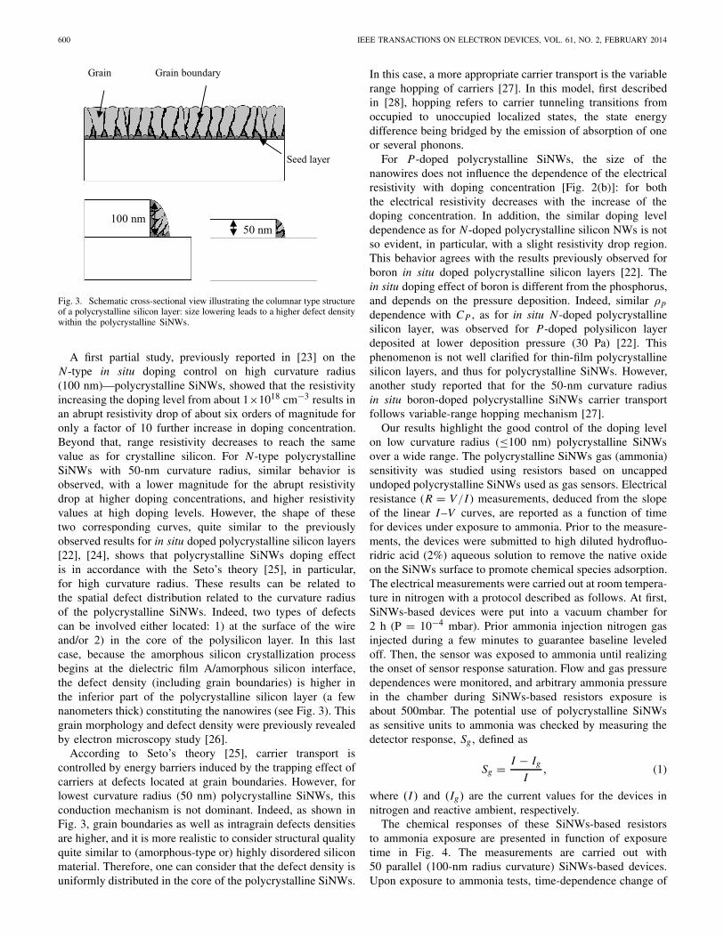
Fig. 3. Schematic cross-sectional view illustrating the columnar type structureof a polycrystalline silicon layer: size lowering leads to a higher defect densitywithin the polycrystalline SiNWs.
A first partial study, previously reported in [23] on theN-type in situ doping control on high curvature radius(100 nm)—polycrystalline SiNWs, showed that the resistivityincreasing the doping level from about 1×1018 cm−3 results inan abrupt resistivity drop of about six orders of magnitude foronly a factor of 10 further increase in doping concentration.Beyond that, range resistivity decreases to reach the samevalue as for crystalline silicon. For N-type polycrystallineSiNWs with 50-nm curvature radius, similar behavior isobserved, with a lower magnitude for the abrupt resistivitydrop at higher doping concentrations, and higher resistivityvalues at high doping levels. However, the shape of thesetwo corresponding curves, quite similar to the previouslyobserved results for in situ doped polycrystalline silicon layers[22], [24], shows that polycrystalline SiNWs doping effectis in accordance with the Seto’s theory [25], in particular,for high curvature radius. These results can be related tothe spatial defect distribution related to the curvature radiusof the polycrystalline SiNWs. Indeed, two types of defectscan be involved either located: 1) at the surface of the wireand/or 2) in the core of the polysilicon layer. In this lastcase, because the amorphous silicon crystallization processbegins at the dielectric film A/amorphous silicon interface,the defect density (including grain boundaries) is higher inthe inferior part of the polycrystalline silicon layer (a fewnanometers thick) constituting the nanowires (see Fig. 3). Thisgrain morphology and defect density were previously revealedby electron microscopy study [26].
According to Seto’s theory [25], carrier transport iscontrolled by energy barriers induced by the trapping effect ofcarriers at defects located at grain boundaries. However, forlowest curvature radius (50 nm) polycrystalline SiNWs, thisconduction mechanism is not dominant. Indeed, as shown inFig. 3, grain boundaries as well as intragrain defects densitiesare higher, and it is more realistic to consider structural qualityquite similar to (amorphous-type or) highly disordered siliconmaterial. Therefore, one can consider that the defect density isuniformly distributed in the core of the polycrystalline SiNWs.
In this case, a more appropriate carrier transport is the variablerange hopping of carriers [27]. In this model, first describedin [28], hopping refers to carrier tunneling transitions fromoccupied to unoccupied localized states, the state energydifference being bridged by the emission of absorption of oneor several phonons.
For P-doped polycrystalline SiNWs, the size of thenanowires does not influence the dependence of the electricalresistivity with doping concentration [Fig. 2(b)]: for boththe electrical resistivity decreases with the increase of thedoping concentration. In addition, the similar doping leveldependence as for N-doped polycrystalline silicon NWs is notso evident, in particular, with a slight resistivity drop region.This behavior agrees with the results previously observed forboron in situ doped polycrystalline silicon layers [22]. Thein situ doping effect of boron is different from the phosphorus,and depends on the pressure deposition. Indeed, similar ρp
dependence with CP , as for in situ N-doped polycrystallinesilicon layer, was observed for P-doped polysilicon layerdeposited at lower deposition pressure (30 Pa) [22]. Thisphenomenon is not well clarified for thin-film polycrystallinesilicon layers, and thus for polycrystalline SiNWs. However,another study reported that for the 50-nm curvature radiusin situ boron-doped polycrystalline SiNWs carrier transportfollows variable-range hopping mechanism [27].
Our results highlight the good control of the doping levelon low curvature radius (≤100 nm) polycrystalline SiNWsover a wide range. The polycrystalline SiNWs gas (ammonia)sensitivity was studied using resistors based on uncappedundoped polycrystalline SiNWs used as gas sensors. Electricalresistance (R = V/I ) measurements, deduced from the slopeof the linear I–V curves, are reported as a function of timefor devices under exposure to ammonia. Prior to the measure-ments, the devices were submitted to high diluted hydrofluo-ridric acid (2%) aqueous solution to remove the native oxideon the SiNWs surface to promote chemical species adsorption.The electrical measurements were carried out at room tempera-ture in nitrogen with a protocol described as follows. At first,SiNWs-based devices were put into a vacuum chamber for2 h (P = 10−4 mbar). Prior ammonia injection nitrogen gasinjected during a few minutes to guarantee baseline leveledoff. Then, the sensor was exposed to ammonia until realizingthe onset of sensor response saturation. Flow and gas pressuredependences were monitored, and arbitrary ammonia pressurein the chamber during SiNWs-based resistors exposure isabout 500mbar. The potential use of polycrystalline SiNWsas sensitive units to ammonia was checked by measuring thedetector response, Sg , defined as
Sg = I − Ig
I, (1)
where (I ) and (Ig) are the current values for the devices innitrogen and reactive ambient, respectively.
The chemical responses of these SiNWs-based resistorsto ammonia exposure are presented in function of exposuretime in Fig. 4. The measurements are carried out with50 parallel (100-nm radius curvature) SiNWs-based devices.Upon exposure to ammonia tests, time-dependence change of

ROGEL et al.: POLYCRYSTALLINE SINWs SYNTHESIS COMPATIBLE WITH CMOS TECHNOLOGY 601
Fig. 4. Variations of the current versus time under controlled ammoniaexposure. The pressure adjusted in the chamber is 500 mbar, and themeasurements are carried out at room temperature. SiNWs radius curvature:100 nm.
the electrical resistance is found to show a quasi-reversibletrend because of the recovery baseline leveled off, suggestingthat polycrystalline SiNWs could be reusable after exposure.Electrical current increases because ammonia species act asdonor of electrons (reducing agents) at the SiNWs surface [29].This behavior was previously observed [30] for such polycrys-talline SiNWs-based resistors under ammonia exposure. In thiscase, after evacuating the vacuum chamber, diluted ammoniainto nitrogen is injected under controlled concentrations (700,350, and 175 ppm) and shows that the detector responseSg increase is proportional to the increase of the ammoniaconcentration. These first quantitative results, acting as proofof concept, show the potential use of polycrystalline SiNWsas gas (ammonia) sensitive units. However, further studiesconcerning sensitivity, low detection limits, and reproducibilityare needed for gas sensors applications.
Such results are explained because the gas moleculesadsorption occurs at the SiNWs surface, the electrons aretransferred to the polycrystalline SiNWs core. Such interac-tions induce significant changes in the carriers transport alongthe nanowires and SiNWs electrical resistance (or current) indifferent possible cumulative ways. First, as the SiNWs con-ductance can be modulated by an applied voltage [29], [31],positively charged gas molecules (electron donors) binded onSiNWs surface can modulate their conductance by changingthe volume of the conductive layer. In this case, ammoniamay act as chemical gates. In other words, it means thatthe Fermi level of the SiNWs is shifted to the conductionband edge reducing the sample electrical resistance. Moreover,carrier transport strongly depends on structural nanowiresdefects. Therefore, we have to consider the effects of grainboundaries. Through charge exchange, gas molecules adsorbedmay play a significant role in decreasing the potential barrierheight at the grain boundaries between two grains. Previouswork reported such effect [32]. In this case, adsorbed gasmolecules passivate defects like dangling bonds leading toan increase of current [33]. The electrical current increaseunder ammonia exposure suggests that electrons transfer and
Fig. 5. (a) Back-gate and (b) top-gate polycrystalline SiNWs-based TFTs.
potential barriers lowering effects may dominate. Such resultsact as a proof of concept and show the potential usefulnessof the polycrystalline SiNWs for high-sensitive gas sensorsapplications operating at room temperature.
N- and P-channel thin-film transistors (TFTs) are fabricatedusing undoped polycrystalline SiNWs following the synthesismethod described previously. In addition, two types of TFTsare studied: 1) back-gate and 2) top-gate devices (Fig. 5). Forback-gate transistors, the substrate is heavily doped crystallinesilicon wafer acting as gate electrode [see Fig. 5(a)]. Thefilm A acting as gate insulator is a 100-nm-thick Si3N4 layerdeposited by LPCVD technique at 600 °C. Source and drainregions are made of heavily in situ N-type (P-type) dopedpolycrystalline silicon layer deposited by LPCVD techniquefor N- and P-channel transistors, respectively. This layer ispatterned by RIE with SF6 plasma before thermal evaporationof aluminum used for source and drain electrodes. For the top-gate TFT [Fig. 5(b)], the (100-nm-thick) SiO2 capping layeracting as a gate insulator is deposited by CVD technique atatmospheric pressure at 420 °C after heavily in situ dopedpolycrystalline silicon source/drain regions plasma patterning,and wet etched for opening contacts. Gate electrode is pat-terned with source and drain electrodes.
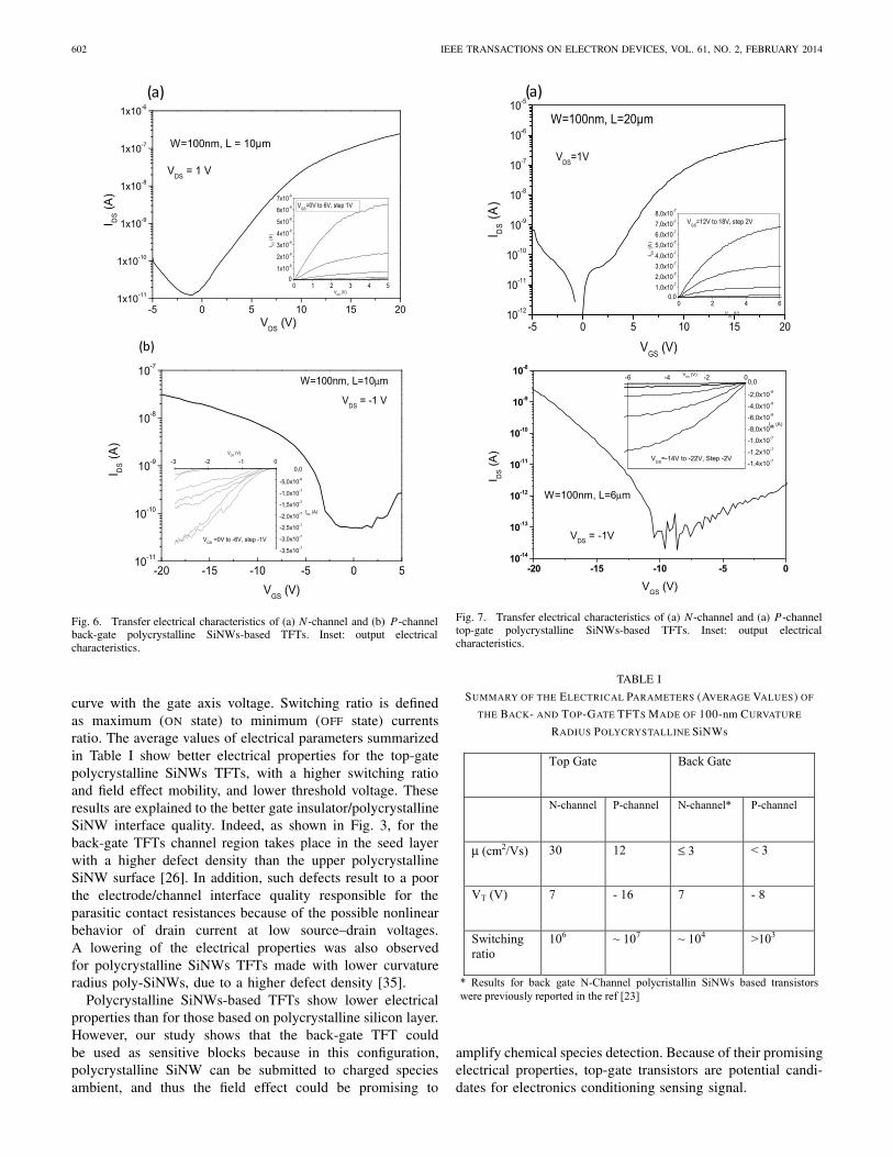
The transfer and output characteristics are shown inFigs. 6 and 7 for the two types 100-nm radius curvaturepolysilicon NWs TFTs. Electrical parameters, thresholdvoltage, VT , and optimum field effect mobility, μ, aredetermined according to the classical conduction electricalmodel used for the metal–oxide–semiconductor field-effecttransistor) [34]. μ is deduced from the maximum slope of theIDS(VGS) curve (transconductance) measured in the saturationmode, and VT is determined by the intercept of the I 1/2
DS (VGS)
602 IEEE TRANSACTIONS ON ELECTRON DEVICES, VOL. 61, NO. 2, FEBRUARY 2014
Fig. 6. Transfer electrical characteristics of (a) N -channel and (b) P-channelback-gate polycrystalline SiNWs-based TFTs. Inset: output electricalcharacteristics.
curve with the gate axis voltage. Switching ratio is definedas maximum (ON state) to minimum (OFF state) currentsratio. The average values of electrical parameters summarizedin Table I show better electrical properties for the top-gatepolycrystalline SiNWs TFTs, with a higher switching ratioand field effect mobility, and lower threshold voltage. Theseresults are explained to the better gate insulator/polycrystallineSiNW interface quality. Indeed, as shown in Fig. 3, for theback-gate TFTs channel region takes place in the seed layerwith a higher defect density than the upper polycrystallineSiNW surface [26]. In addition, such defects result to a poorthe electrode/channel interface quality responsible for theparasitic contact resistances because of the possible nonlinearbehavior of drain current at low source–drain voltages.A lowering of the electrical properties was also observedfor polycrystalline SiNWs TFTs made with lower curvatureradius poly-SiNWs, due to a higher defect density [35].
Polycrystalline SiNWs-based TFTs show lower electricalproperties than for those based on polycrystalline silicon layer.However, our study shows that the back-gate TFT couldbe used as sensitive blocks because in this configuration,polycrystalline SiNW can be submitted to charged speciesambient, and thus the field effect could be promising to
Fig. 7. Transfer electrical characteristics of (a) N -channel and (a) P-channeltop-gate polycrystalline SiNWs-based TFTs. Inset: output electricalcharacteristics.
TABLE I
SUMMARY OF THE ELECTRICAL PARAMETERS (AVERAGE VALUES) OF
THE BACK- AND TOP-GATE TFTS MADE OF 100-nm CURVATURE
RADIUS POLYCRYSTALLINE SiNWs
amplify chemical species detection. Because of their promisingelectrical properties, top-gate transistors are potential candi-dates for electronics conditioning sensing signal.
ROGEL et al.: POLYCRYSTALLINE SINWs SYNTHESIS COMPATIBLE WITH CMOS TECHNOLOGY 603
IV. CONCLUSION
This paper shows the great flexibility in design of planarSiNWs array by direct patterning technique using conventionallithographic tools. The N- and P-type polycrystalline SiNWsdoping control make them good candidates for the fabricationof electrically controlled thin-film devices (resistors and tran-sistors), in particular, for specific gas (reducing) sensing orelectronics applications.
The results show the full compatibility of the nanospacerpoly-SiNWs technology with the existing silicon CMOS tech-nology, using nanowires as potential sensitive units for inte-grated gas sensor applications. Indeed, field-effect behaviorobserved in polycrystalline SiNWs-based transistors is promis-ing to amplify chemical species detection as well as forelectronics conditioning sensing signal for back- and top-gateconfigurations, respectively.
In addition, because of silicon surface functionalization pos-sibilities, such results offer a great potential for further devel-opments of integrated SiNWs-based (bio)chemical sensors andtheir implementation in electronic systems.
REFERENCES
[1] J. Goldberger, A. I. Hochbaum, R. Fan, and P. Yang, “Silicon verticallyintegrated nanowire field effect transistors,” Nanoletters, vol. 6, no. 5,pp. 973–977, 2006.
[2] C. Yang, C. J. Barrelet, F. Capasso, and C. M. Lieber, “Singlep-type/intrinsic/n-type silicon nanowires as nanoscale avalanchephotodetectors,” Nanoletters, vol. 6, no. 12, pp. 2929–2934, 2006.
[3] Y. Cui, Q. Wei, H. K. Park, and C. M. Lieber, “Nanowire nanosensorsfor highly sensitive and selective detection of biological and chemicalspecies,” Science, vol. 293, no. 5533, pp. 1289–1292, 2001.
[4] Z. Li, Y. Chen, X. Li, T. I. Kamins, K. Nauka, and R. S. Williams,“Sequence-specific label-free DNA sensors based on silicon nanowires,”Nanoletters, vol. 4, no. 2, pp. 245–247, 2004.
[5] H. J. In, C. R. Field, and P. E. Pehrsson, “Periodically porous topelectrodes on vertical nanowire arrays for highly sensitive gas detection,”Nanotechnology, vol. 22, pp. 355501-1–355501-5, 2011.
[6] M. C. McAlpine, H. Ahmad, D. Wang, and J. R. Heath, “Highly orderednanowires arrays on plastic substrates for ultrasensitive flexible chemicalsensors,” Nature Mater., vol. 6, pp. 379–384, Apr. 2007.
[7] M. Cuscuna, A. Convertino, E. Zampetti, A. Macagnano, A. Pec-ora, G. Fortunato, et al., “On-chip fabrication of ultrasensitive NO2sensors based on silicon nanowires,” Appl. Phys. Lett., vol. 101,pp. 103101-1–103101-5, Sep. 2012.
[8] Y. Liu and T. Cui, “Silica nanowires fabricated with layer-by-layerself-assembled nanoparticles,” J. Nanosci. Nanotechnol., vol. 6, no. 4,pp. 1019–1023, 2006.
[9] P. Cheyssac, M. Sacilotti, and G. Patriarche, “Vapor-liquid-solid mech-anisms: Challenges for nanosized quantum cluster/dot/wire materials,”J. Appl. Phys., vol. 100, pp. 044315-1–044315-12, Aug. 2006.
[10] L. Yu, and P. Roca i Cabarrocas, “Growth mechanism and dynamicsof in-plane solid-liquid-solid silicon nanowires,” Phys. Rev. B, vol. 81,pp. 085323-1–085323-11, Feb. 2010.
[11] I. Michelakaki, A. G. Nassiopoulou, E. Stavrinidou, K. Breza, andN. Frangis, “Porous anodic alumina on galvanically grown PtSi layerfor application in template-assisted Si nanowire growth,” Nanoscale Res.Lett., vol. 6, p. 414, Jun. 2011.
[12] H. Xiang-Lei, L. Guilhem, F. Pier-Francesco, and D. Emmanuel, Micro-electr. Eng., vol. 88, no. 8, p. 2622, 2011.
[13] I. Ionica, L. Montes, S. Ferraton, J. Zimmermann, L. Saminadayar,and V. Bouchiat, “Field effect and Coulomb blockage in silicon oninsulator nanostructures fabricated by atomic force microscope,” Solid-State Electron., vol. 49, no. 9, pp. 1497–1507, 2005.
[14] L. Pichon, R. Rogel, and F. Demami, “Fabrication of amorphous siliconnanoribbons by atomic force microscope tip-induced local oxidation forthin film device applications,” Semicond. Sci. Technol., vol. 25, no. 6,pp. 065001-1–065001-5, 2010.
[15] L. Yang, D. H. Lee, Y. H. Chen, C. Y. Chang, S. D. Liu, and C. C. Huang,“5 nm-gate nanowire FinFET,” in VLSI Symp. Tech. Dig., 2004, p. 196.
[16] S. Y. Chou, R. Krauss, and P. J. Renstrom, “Nanoscale silicon fieldeffect transistors fabricated using imprint lithography,” Science, vol. 85,p. 272, Apr. 1996.
[17] A. Talin, L. Hunter, F. Léonard, and B. Rokad, “Large area, densesilicon nanowire array chemical sensors,” Appl. Phys. Lett., vol. 89,pp. 153102-1–153102-3, Oct. 2006.
[18] M. Lee, Y. Jeon, T. Moon, and S. Kim, “Top-down fabrication of fullyCMOS-compatible silicon nanowire arrays and their integration intoCMOS inverters on plastic,” ACS Nano, vol. 5, no. 4, pp. 2629–2636,2011.
[19] K. D. Buddharaju, N. Singh, S. C. Rustagi, S. H. G. Teo, G. Q. Lo,N. Balasubramanian, et al., “Si-nanowire CMOS inverter logic fabricatedusing gate-all-around (GAA) devices and top-down approach,” Solid-State Electron., vol. 52, no. 9, pp. 1312–1317, 2008.
[20] F. Wessely, T. Krauss, and U. Schwalke, “CMOS without doping:Multi-gate silicon-nanowire fiel effect transistors,” Solid-State Electron.,vol. 70, pp. 33–38, Apr. 2012.
[21] F. Demami, L. Pichon, R. Rogel, and A. C. Salaun, “Fabrication andelectrical characterization of silicon nanowires based resistors,” IOPConf. Ser., Mater. Sci. Eng., vol. 6, no. 1, p. 012014, 2009.
[22] D. Briand, M. Sarret, F. Le Bihan, O. Bonnaud, and L. Pichon,“Polysilicon in situ phosphorus doping control over large concentrationrange using low temperature, low pressure chemical vapour depositiongrowth process,” Mater. Sci. Technol., vol. 11, no. 11, pp. 1207–1209,1995.
[23] F. Demami, R. Rogel, A. C. Salaun, and L. Pichon, “Electrical propertiesof polysilicon nanowires for devices applications,” Phys. Status Solidi,vol. 8, no. 3, pp. 827–830, 2011.
[24] D. Briand, “Silicium déposé par LPCVD et dopé in-situ: Dépôt,caractérisation et application,” Ph.D. dissertation, Dept. Groupe deMicroélectronique et visualisation, Université de Rennes 1, Rennes,France, 1995.
[25] J. W. Seto, “The electrical properties of pollycrystalline silicon films,”J. Appl. Phys., vol. 46, no. 12, pp. 5247–5254, 1975.
[26] L. Haji, P. Joubert, J. Stoemenos, and N. A. Economou, “Mode of growthand microstructure of polycrystalline silicon obtained by solid-phasecrystallization of an amorphous silicon film,” J. Appl. Phys., vol. 75,no. 8, pp. 3944–3952, 1994.
[27] L. Pichon, E. Jacques, R. Rogel, A. C. Salaun, and F. Demami,“Variable range hopping conduction in N- and P-type in situ dopedpolycrystalline silicon nanowires,” Semicond. Sci. Technol., vol. 28,pp. 025002-1–025002-6, 2013.
[28] N. F. Mott, “Conduction in non-crystalline materials: III. Localized statesin a pseudogap and near extremities of conduction and valence bands,”Phil. Mag., vol. 19, no. 160, pp. 835–852, 1969.
[29] A. A. Talin, L. L. Hunter, F. Leonard, and B. Rokad, “Large area, densesilicon nanowire array chemical sensors,” Appl. Phys. Lett., vol. 89,no. 15, pp. 153102-1–153102-3, 2006.
[30] F. Demami, L. Ni, R. Rogel, A. C. Salaun, and L. Pichon, “Siliconnanowires based resistors as gas sensors,” Sens. Actuators B, Chem.,vol. 170, pp. 158–162, Jul. 2012.
[31] J. Y. Yu, S. W. Chung, and J. R. Heath, “Silicon naowires: Preparation,device fabrication, and transport properties,” J. Phys. Chem, B, vol. 104,no. 50, pp. 11864–11870, 2000.
[32] Y. Shimizu and M. Egashira, “Basic aspects and challenges of semicon-ductor gas sensors,” MRS Bull., vol. 24, pp. 18–24 Jun. 1999.
[33] N. K. Ali, M. R. Hashim, and A. A. Aziz, “Effects of surface passivationin porous silicon as H2 gas sensor,” Solid.-State Electron., vol. 52, no. 7,pp. 1017–1074, 2008.
[34] S. M. Sze, Physics of Semiconductor Devices, 2nd ed. New York, NY,USA: Wiley, 1981, p. 442.
[35] F. Demami, “Synthèse de nanofils de silicium par la méthodedes espaceurs pour dispositifs électroniques,” Ph.D. dissertation,Dept. Microélectronique et Microcapteurs, Université de Rennes1,Rennes, France, 2011.
Regis Rogel received the Ph.D. degree in electronics from Université deRennes 1, Rennes, France, in 2001.
He is currently with Institut d’Electronique et des Télécommunications deRennes, Rennes. His current research interests include electrical characteriza-tion of silicon nanowire based devices for sensor or electronic applications.
604 IEEE TRANSACTIONS ON ELECTRON DEVICES, VOL. 61, NO. 2, FEBRUARY 2014
Emmanuel Jacques received the Ph.D. degree in electronics from Instituted’Electronique et Télécommunications of Rennes, Rennes, France, in 2008.
He is an Assistant Professor with the University of Rennes, Rennes. Hiscurrent research interests include the technological process optimization oflow temperature electronic devices and the study of polysilicon nanowiresmade for sensor applications and electronic devices.
Laurent Pichon received the Ph.D. degree in physics from the Universityof Rennes, Rennes, France, in 1993, and the Habilitation à Diriger desRecherches degree in electronics from the University of Caen, Caen, France,in 2001.
He has been a Professor with the Departement Microelectronique etMicroscapteurs, Institut d’Electronique et des Télécommunications de Rennes,University of Rennes, since 2005. His current research interests include siliconnanowires technology for electronics and sensors.
Anne Claire Salaun received the Docteur-es-science Physique degree fromthe University of Rennes, Rennes, France, in 1996.
She has been an Associate Professor with Institut d’Electronique et deTelecommunications de Rennes, Rennes, since 1998. Her work is devoted tomicrotechnology, with applications to chemical and biological sensors.