Embed Size (px)
Citation preview
Polarization-independent waveguiding with annular photonic crystals
Ahmet Cicek and Bulent Ulug*
Department of Physics, Faculty of Arts and Sciences, Akdeniz University, Campus 07058, Antalya/Turkey *[email protected]
Abstract: A linear waveguide in an annular photonic crystal composed of a square array of annular dielectric rods in air is demonstrated to guide transverse electric and transverse magnetic modes simultaneously. Overlapping of the guided bands in the full band gap of the photonic crystal is shown to be achieved through an appropriate set of geometric parameters. Results of Finite-Difference Time-Domain simulations to demonstrate polarization-independent waveguiding with low loss and wavelength-order confinement are presented. Transmission through a 90° bend is also demonstrated.
©2009 Optical Society of America
OCIS codes: (130.5296) Photonic crystal waveguides; (230.5298) Photonic crystals.
References and links
1. E. Lidorikis, M. L. Povinelli, S. G. Johnson, and J. D. Joannopoulos, “Polarization-independent linear waveguides in 3D photonic crystals,” Phys. Rev. Lett. 91(2), 023902 (2003).
2. Y. Xu, X.-J. Chen, S. Lan, Q.-F. Dai, Q. Guo, and L.-J. Wu, “Polarization-independent self-collimation based on pill-void photonic crystals with square symmetry,” Opt. Express 17(6), 4903–4912 (2009), http://www.opticsinfobase.org/oe/abstract.cfm?uri=oe-17-6-4903.
3. A. Mekis, S. Fan, and J. D. Joannopoulos, “Bound states in photonic crystal waveguides and waveguide bends,” Phys. Rev. B 58(8), 4809–4817 (1998).
4. N. Susa, “Large absolute and polarization-independent photonic band gaps for various lattice structures and rod shapes,” J. Appl. Phys. 91(6), 3501 (2002).
5. J. D. Joannopoulos, S. G. Johnson, J. N. Winn, and R. D. Meade, Photonic Crystals: Molding the Flow of Light (2nd Ed., Princeton University Press, 2008), pp. 242–251.
6. H. Kurt, and D. S. Citrin, “Annular photonic crystals,” Opt. Express 13(25), 10316–10326 (2005), http://www.opticsexpress.org/abstract.cfm?URI=OPEX-13-25-10316.
7. W. H. Press, S. A. Teukolsky, W. T. Wetterling, and B. P. Flannery, Numerical Recipes: The Art of Scientific Computing (3rd Ed., Cambridge University Press, 2007), pp. 502–507.
8. K. S. Yee, “Numerical solutions of initial boundary value problems involving Maxwell’s equations in isotropic media,” IEEE Trans. Antenn. Propag. 14(3), 302–307 (1966).
9. K. M. Ho, C. T. Chan, and C. M. Soukoulis, “Existence of a photonic gap in periodic dielectric structures,” Phys. Rev. Lett. 65(25), 3152–3155 (1990).
10. RSoft Design Group, http://www.rsoftdesign.com. 11. J. P. Berenger, “Perfectly matched layer for the absorption of electromagnetic waves,” J. Comput. Phys. 114(2),
185–200 (1994). 12. L. H. Frandsen, A. V. Lavrinenko, J. Fage-Pedersen, and P. I. Borel, “Photonic crystal waveguides with semi-
slow light and tailored dispersion properties,” Opt. Express 14(20), 9444–9450 (2006), http://www.opticsinfobase.org/oe/abstract.cfm?uri=oe-14-20-9444.
13. Y. A. Vlasov, M. O’Boyle, H. F. Hamann, and S. J. McNab, “Active control of slow light on a chip with photonic crystal waveguides,” Nature 438(7064), 65–69 (2005).
14. T. Baba, “Slow light in photonic crystals,” Nat. Photonics 2(8), 465–473 (2008).
1. Introduction
Polarization-independent waveguiding is an important requirement in integrated optics [1] and is desirable to be accomplished in two-dimensional (2D) photonic crystals (PC) due to manufacturing and applicability concerns. Polarization-independent waveguiding in 2D PCs without defects is possible via self collimation by overlapping first transverse electric (TE) and transverse magnetic (TM) bands through modifying the PC geometry [2], where TE/TM designates magnetic/electric field vector normal to the plane of PC.
(C) 2009 OSA 28 September 2009 / Vol. 17, No. 20 / OPTICS EXPRESS 18381#116152 - $15.00 USD Received 24 Aug 2009; revised 14 Sep 2009; accepted 14 Sep 2009; published 25 Sep 2009
Linear defect (or briefly linear) waveguides (WG) are appropriate for guiding light in the band gap of a PC with low loss [3]. Polarization-independent waveguiding by a linear WG in a 2D PC requires a full band gap in which TE and TM band gaps overlap. However, a full band gap may be obtained for a limited range of physical parameters [4].
TE band gaps occur more likely in a lattice of connected dielectric regions containing isolated air holes, whereas TM gaps are preferred in a lattice of individual dielectric regions in air [1,4–6]. Based on this fact, a three-dimensional (3D) layered structure composed of alternating layers of 2D slab PCs, each comprising a linear WG for either TE or TM polarization, is utilized for polarization-independent waveguiding [1]. In this design, TM mode is guided in the half layer of dielectric rods in air, whereas TE mode is guided in the adjacent half layer with air holes in dielectric slab [1].
Annular PCs [6] are 2D lattices of annular dielectric rods in air or annular air voids in dielectric background, which can be thought as the combination of the two half layers in the structure of ref [1]. in 2D. Linear WGs hosted in annular PCs could be good candidates for polarization-independent waveguiding in 2D due to large full band gaps offered.
In this work, optimization of the geometric parameters of a linear WG in an annular PC is carried out by means of Nelder-Mead (downhill simplex) algorithm [7] to accomplish polarization-independent waveguiding in 2D. Finite-Difference Time-Domain (FDTD) simulations [8] are conducted to demonstrate polarization-independent waveguiding and transmission through a 90° bend.
2. Guided Bands
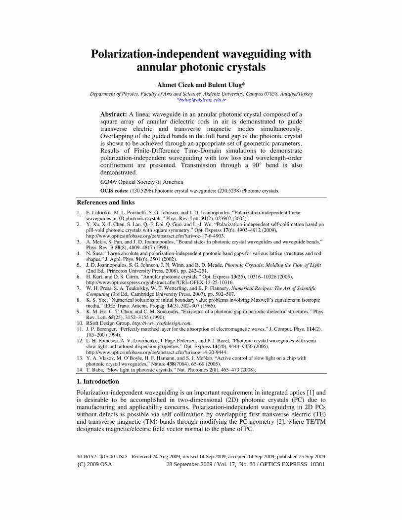
Annular PC composed of a square lattice of annular dielectric rods (ε1 = 13) in air (ε0) is depicted in Fig. 1a. Inner and outer radii of the rods are denoted by rin and rout, respectively. Band structure of the unit cell in Fig. 1a is computed by Plane Wave Expansion (PWE) Method [9], via RSoft Design Group’s BandSOLVE software [10], and is given in Fig. 1b.
Fig. 1. (a) Details of the 21x1 super cell employed in computations and (b) the band structure of the unit cell marked by the dashed box in (a).
Full band gap shown in Fig. 1b is largest with 6.741% gap ratio between normalized angular frequencies (ωnorm = ωa/2πc) 0.522 and 0.558 for rin = 0.251a and rout = 0.396a. Lattice constant a is 0.702µm, at which the targeted free-space wavelength λ0 = 1.3µm coincides with the center of the full band gap.
Linear WG seen in Fig. 1a, which is a linear array of circular dielectric rods (ε1 = 13) with elliptical air holes at their centers, is defined by four parameters: radius (rwg) of the dielectric rods, semimajor axes (sa and sb) of the elliptical air holes and the change in the half width of the WG (∆w). Guided bands are obtained by computing the projected band structure for the wave vectors along the WG direction [3]. A 21x1 super cell is employed in the computations to avoid overlapping of the field components of adjacent super cells.
Nelder-Mead (simplex) algorithm [7] is employed to achieve maximal overlapping for the guided bands by a search within the parameter space {rwg, sa, sb, ∆w}. The algorithm seeks for a local minimum of an entity by varying only one parameter at a time. Iterations progress over each parameter until all parameters converge and restart from the first parameter until the entity both converges and falls below a predefined value. In the implementation, investigated
(C) 2009 OSA 28 September 2009 / Vol. 17, No. 20 / OPTICS EXPRESS 18382#116152 - $15.00 USD Received 24 Aug 2009; revised 14 Sep 2009; accepted 14 Sep 2009; published 25 Sep 2009
entity denoted by Σ(∆ωnorm)2 is the sum of squares of the differences in normalized angular
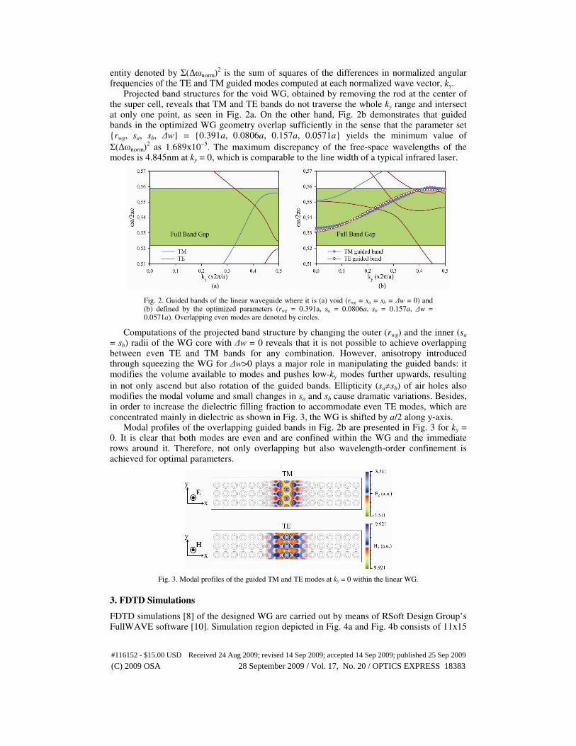
frequencies of the TE and TM guided modes computed at each normalized wave vector, ky. Projected band structures for the void WG, obtained by removing the rod at the center of
the super cell, reveals that TM and TE bands do not traverse the whole ky range and intersect at only one point, as seen in Fig. 2a. On the other hand, Fig. 2b demonstrates that guided bands in the optimized WG geometry overlap sufficiently in the sense that the parameter set {rwg, sa, sb, ∆w} = {0.391a, 0.0806a, 0.157a, 0.0571a} yields the minimum value of
Σ(∆ωnorm)2 as 1.689x10
−5. The maximum discrepancy of the free-space wavelengths of the
modes is 4.845nm at ky = 0, which is comparable to the line width of a typical infrared laser.
Fig. 2. Guided bands of the linear waveguide where it is (a) void (rwg = sa = sb = ∆w = 0) and (b) defined by the optimized parameters (rwg = 0.391a, sa = 0.0806a, sb = 0.157a, ∆w = 0.0571a). Overlapping even modes are denoted by circles.
Computations of the projected band structure by changing the outer (rwg) and the inner (sa = sb) radii of the WG core with ∆w = 0 reveals that it is not possible to achieve overlapping between even TE and TM bands for any combination. However, anisotropy introduced through squeezing the WG for ∆w>0 plays a major role in manipulating the guided bands: it modifies the volume available to modes and pushes low-ky modes further upwards, resulting
in not only ascend but also rotation of the guided bands. Ellipticity (sa≠sb) of air holes also modifies the modal volume and small changes in sa and sb cause dramatic variations. Besides, in order to increase the dielectric filling fraction to accommodate even TE modes, which are concentrated mainly in dielectric as shown in Fig. 3, the WG is shifted by a/2 along y-axis.
Modal profiles of the overlapping guided bands in Fig. 2b are presented in Fig. 3 for ky = 0. It is clear that both modes are even and are confined within the WG and the immediate rows around it. Therefore, not only overlapping but also wavelength-order confinement is achieved for optimal parameters.
Fig. 3. Modal profiles of the guided TM and TE modes at ky = 0 within the linear WG.
3. FDTD Simulations
FDTD simulations [8] of the designed WG are carried out by means of RSoft Design Group’s FullWAVE software [10]. Simulation region depicted in Fig. 4a and Fig. 4b consists of 11x15
(C) 2009 OSA 28 September 2009 / Vol. 17, No. 20 / OPTICS EXPRESS 18383#116152 - $15.00 USD Received 24 Aug 2009; revised 14 Sep 2009; accepted 14 Sep 2009; published 25 Sep 2009
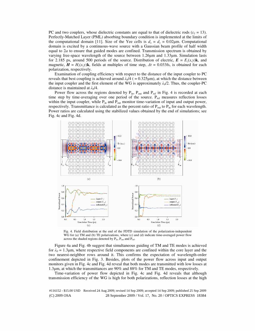
PC and two couplers, whose dielectric constants are equal to that of dielectric rods (ε1 = 13). Perfectly-Matched Layer (PML) absorbing boundary condition is implemented at the limits of the computational domain [11]. Size of the Yee cells is dx = dy = 0.02µm. Computational domain is excited by a continuous-wave source with a Gaussian beam profile of half width equal to 2a to ensure that guided modes are confined. Transmission spectrum is obtained by varying free-space wavelength of the source between 1.26µm and 1.33µm. Simulation lasts for 2.185 ps, around 500 periods of the source. Distribution of electric, E = Ez(x,y)k, and magnetic, H = Hz(x,y)k, fields at multiples of time step, ∆t = 0.033fs, is obtained for each polarization, respectively.
Examination of coupling efficiency with respect to the distance of the input coupler to PC reveals that best coupling is achieved around λ0/4 ( = 0.325µm), at which the distance between the input coupler and the first element of the WG is approximately λ0/2. Thus, the coupler-PC distance is maintained at λ0/4.
Power flow across the regions denoted by Pin, Pout and Pref in Fig. 4 is recorded at each time step by time-averaging over one period of the source. Pref measures reflection losses within the input coupler, while Pin and Pout monitor time-variation of input and output power, respectively. Transmittance is calculated as the percent ratio of Pout to Pin for each wavelength. Power ratios are calculated using the stabilized values obtained by the end of simulations; see Fig. 4c and Fig. 4d.
Fig. 4. Field distribution at the end of the FDTD simulation of the polarization-independent WG for (a) TM and (b) TE polarizations, where (c) and (d) indicate time-averaged power flow across the shaded regions denoted by Pin, Pout and Pref.
Figure 4a and Fig. 4b suggest that simultaneous guiding of TM and TE modes is achieved for λ0 = 1.3µm, where respective field components are confined within the core layer and the two nearest-neighbor rows around it. This confirms the expectation of wavelength-order confinement depicted in Fig. 3. Besides, plots of the power flow across input and output monitors given in Fig. 4c and Fig. 4d reveal that both modes are transmitted with low losses at 1.3µm, at which the transmittances are 90% and 88% for TM and TE modes, respectively.
Time-variation of power flow depicted in Fig. 4c and Fig. 4d reveals that although transmission efficiency of the WG is high for both polarizations, reflection losses at the high
(C) 2009 OSA 28 September 2009 / Vol. 17, No. 20 / OPTICS EXPRESS 18384#116152 - $15.00 USD Received 24 Aug 2009; revised 14 Sep 2009; accepted 14 Sep 2009; published 25 Sep 2009
dielectric-air interface of the input coupler, which are around 30%, are not avoided. Moreover, it is seen in Fig. 3 that energy of the TM mode is mainly concentrated in the low-index region, whereas TE mode favors the dielectric material. This leads to higher confinement of the TE mode. On the other hand, the air gap between the input coupler and PC (λ0/4) poses difficulty in coupling to the TE mode of the WG.
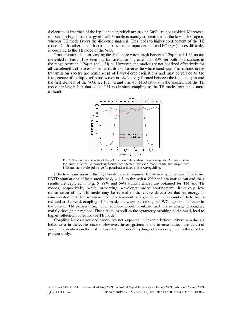
Transmittance data for varying the free-space wavelength between 1.26µm and 1.33µm are presented in Fig. 5. It is seen that transmittance is greater than 80% for both polarizations in the range between 1.28µm and 1.31µm. However, the modes are not confined effectively for all wavelengths of interest since bands do not traverse the whole band gap. Fluctuations in the transmission spectra are reminiscent of Fabry-Perot oscillations and may be related to the interference of multiply-reflected waves in ~λ0/2 cavity formed between the input coupler and the first element of the WG, see Fig. 4a and Fig. 4b. Fluctuations in the spectrum of the TE mode are larger than that of the TM mode since coupling to the TE mode from air is more difficult.
Fig. 5. Transmission spectra of the polarization-independent linear waveguide. Arrows indicate the onset of effective wavelength-order confinement for each mode, while the grayed area indicates the wavelength range for polarization-independent waveguiding.
Effective transmission through bends is also required for device applications. Therefore, FDTD simulations of both modes at λ0 = 1.3µm through a 90° bend are carried out and their results are depicted in Fig. 6. 88% and 56% transmittances are obtained for TM and TE modes, respectively, while preserving wavelength-order confinement. Relatively low transmission of the TE mode may be related to the above discussion that its energy is concentrated in dielectric where mode confinement is larger. Since the amount of dielectric is reduced at the bend, coupling of the modes between the orthogonal WG segments is better in the case of TM polarization, which is more loosely confined and whose energy propagates mainly through air regions. These facts, as well as the symmetry breaking at the bend, lead to higher reflection losses for the TE mode.
Coupling issues discussed above are not expected in inverse lattices, where annular air holes exist in dielectric matrix. However, investigations in the inverse lattices are deferred since computations in these structures take considerably longer times compared to those of the present study.
(C) 2009 OSA 28 September 2009 / Vol. 17, No. 20 / OPTICS EXPRESS 18385#116152 - $15.00 USD Received 24 Aug 2009; revised 14 Sep 2009; accepted 14 Sep 2009; published 25 Sep 2009
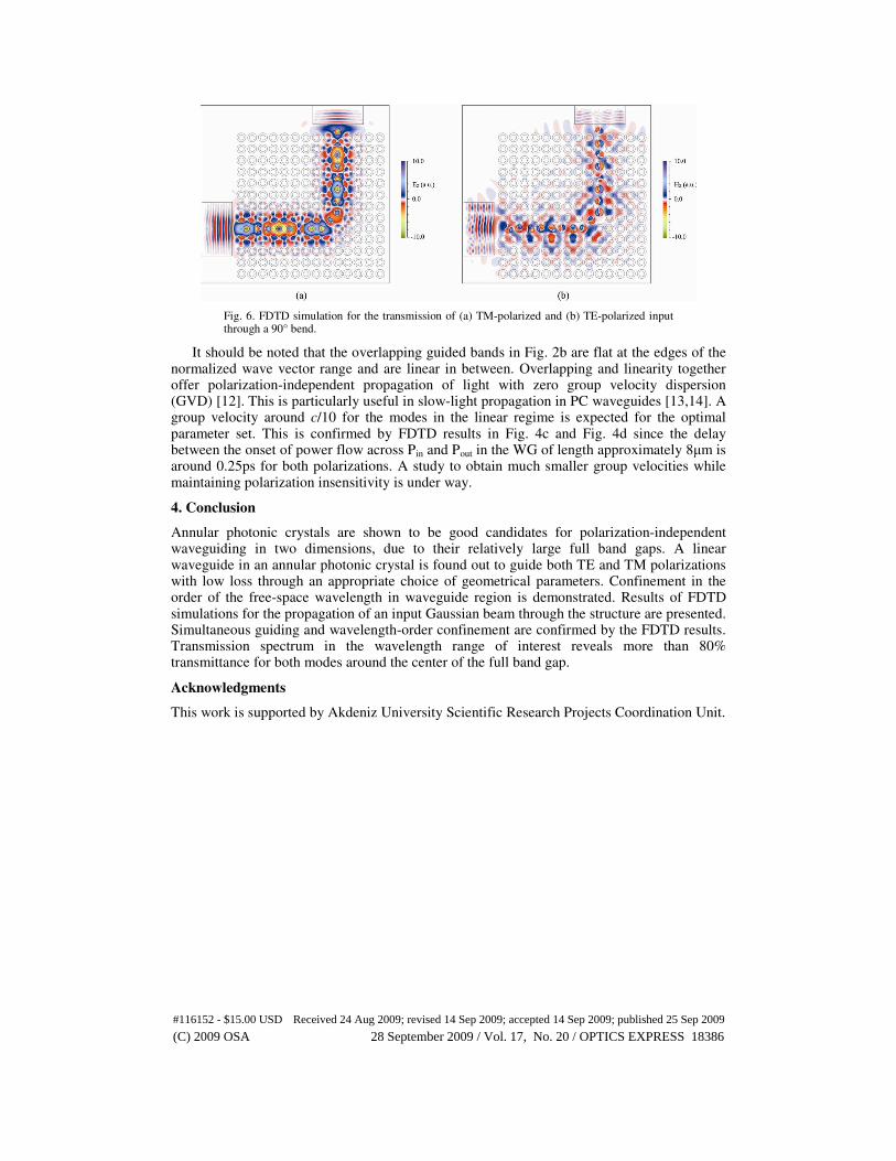
Fig. 6. FDTD simulation for the transmission of (a) TM-polarized and (b) TE-polarized input through a 90° bend.
It should be noted that the overlapping guided bands in Fig. 2b are flat at the edges of the normalized wave vector range and are linear in between. Overlapping and linearity together offer polarization-independent propagation of light with zero group velocity dispersion (GVD) [12]. This is particularly useful in slow-light propagation in PC waveguides [13,14]. A group velocity around c/10 for the modes in the linear regime is expected for the optimal parameter set. This is confirmed by FDTD results in Fig. 4c and Fig. 4d since the delay between the onset of power flow across Pin and Pout in the WG of length approximately 8µm is around 0.25ps for both polarizations. A study to obtain much smaller group velocities while maintaining polarization insensitivity is under way.
4. Conclusion
Annular photonic crystals are shown to be good candidates for polarization-independent waveguiding in two dimensions, due to their relatively large full band gaps. A linear waveguide in an annular photonic crystal is found out to guide both TE and TM polarizations with low loss through an appropriate choice of geometrical parameters. Confinement in the order of the free-space wavelength in waveguide region is demonstrated. Results of FDTD simulations for the propagation of an input Gaussian beam through the structure are presented. Simultaneous guiding and wavelength-order confinement are confirmed by the FDTD results. Transmission spectrum in the wavelength range of interest reveals more than 80% transmittance for both modes around the center of the full band gap.
Acknowledgments
This work is supported by Akdeniz University Scientific Research Projects Coordination Unit.
(C) 2009 OSA 28 September 2009 / Vol. 17, No. 20 / OPTICS EXPRESS 18386#116152 - $15.00 USD Received 24 Aug 2009; revised 14 Sep 2009; accepted 14 Sep 2009; published 25 Sep 2009


![Prof. D. R. Wilton Notes 19 Waveguiding Structures Waveguiding Structures ECE 3317 [Chapter 5]](https://img.pdfslide.us/doc/110x75/56649e975503460f94b9aba9/prof-d-r-wilton-notes-19-waveguiding-structures-waveguiding-structures-ece.jpg)