Embed Size (px)
Citation preview
Timer/Counter/AnalyzerPM6690
Service Manual

II
4822 872 20306May 2006 - Fourth Edition
© Fluke Corporation. All rights reserved.
Printed in Sweden.
GENERAL INFORMATION
Method of Notation
This manual contains directions and information that apply to the PM6690 Timer/Counter/Analyzer. In order to simplify the references,
the following designation system is used throughout the manual:
– PM6690 is abbreviated to '90'.
Warranty
The Warranty Statement is included in the Getting Started Manual.
Declaration of Conformity
The complete text with formal statements concerning product identification, manufacturer and standards used for type testing is avail-
able on request.
Hardware Versions
This Service Manual provides Source of Supply information for the Fluke Model PM6690 Timer/Counter/Analyzer, which may con-
tain an OLD version of the Main CCA, called Version A, or a NEW version of the Main CCA, called Version B. Both the old and the
new version of the Main CCAhave the same part number. All orders for the old version of the Main CCAwill be filled with the new ver-
sion of the Main CCA. When the old version of the Main CCA is returned to the factory for repair, the new version of the Main CCA
will be returned in place of the old version of the Main CCA, if the microprocessor has to be replaced.
Devices with serial numbers up to and including 916779 are equipped with a Triscend microprocessor, whereas devices with higher se-
rial numbers have a Sharp microprocessor. Both are based on an ARM7 core, and from the operator’s point of view the behavior is not
affected. However, essential parts of the main PCB differ, and the corresponding sections of the service manual are consequently af-
fected. Even though large parts of the hardware are common to both versions, we have preferred to divide the pertinent chapters into
separate sections, where certain parts are repeated, all in order to improve legibility and simplify troubleshooting.
Version A refers to devices equipped with the Triscend microprocessor.
Version B refers to devices equipped with the Sharp microprocessor.
The chapters that need special attention are:
Chapter 4, Circuit Descriptions
Chapter 6, Repair
Chapter 8, Replacement Parts
Chapter 9, Schematic Diagrams
� Firmware Compatibility
Despite the relatively large hardware differences, we have managed to integrate the firmware, so that future upgrades can be applied to
both versions by means of the same hex file. Thus there is no need to check the serial number or else find out which processor is inside
the cover. Just proceed according to the instructions given in Chapter 5, Corrective & Preventive Maintenance.
III

This page is intentionally left blank.
IV
Contents
GENERAL INFORMATION. . . . . . . . . . . . . . . . . . . . . III
1 Safety Instructions
Caution and Warning Statements . . . . . . . . . . . . . . . 1-2
Grounding . . . . . . . . . . . . . . . . . . . . . . . . . . . . . . . . . 1-2
Operation . . . . . . . . . . . . . . . . . . . . . . . . . . . . . . . . . 1-2
Line Voltage . . . . . . . . . . . . . . . . . . . . . . . . . . . . . . . 1-4
2 Performance Check
General Information . . . . . . . . . . . . . . . . . . . . . . . . . 2-2
Test Equipment. . . . . . . . . . . . . . . . . . . . . . . . . . . . . 2-2
Preparations . . . . . . . . . . . . . . . . . . . . . . . . . . . . . . . 2-2
Front Panel Controls . . . . . . . . . . . . . . . . . . . . . . . . . 2-2
Short Form Specification Test. . . . . . . . . . . . . . . . . . 2-4
Rear Inputs/Outputs . . . . . . . . . . . . . . . . . . . . . . . . . 2-6
Measuring Functions. . . . . . . . . . . . . . . . . . . . . . . . . 2-6
Check of HOLD OFF Function . . . . . . . . . . . . . . . . . 2-7
RF Options . . . . . . . . . . . . . . . . . . . . . . . . . . . . . . . . 2-7
3 Disassembly
Removing the Cover . . . . . . . . . . . . . . . . . . . . . . . . . 3-2
Fan . . . . . . . . . . . . . . . . . . . . . . . . . . . . . . . . . . . . . . 3-3
Prescaler Options . . . . . . . . . . . . . . . . . . . . . . . . . . . 3-3
OCXO Options . . . . . . . . . . . . . . . . . . . . . . . . . . . . . 3-4
4 Circuit Descriptions
Version A . . . . . . . . . . . . . . . . . . . . . . . . . . . . . . . . . . 4-3
Block Diagram Description . . . . . . . . . . . . . . . . . . . . 4-4
General . . . . . . . . . . . . . . . . . . . . . . . . . . . . . . . . . . . 4-4
Block Diagram . . . . . . . . . . . . . . . . . . . . . . . . . . . . . 4-4
Hardware Functional Description . . . . . . . . . . . . . . . 4-6
Front Unit . . . . . . . . . . . . . . . . . . . . . . . . . . . . . . . . . 4-6
Main Board . . . . . . . . . . . . . . . . . . . . . . . . . . . . . . . . 4-6
Test Routines . . . . . . . . . . . . . . . . . . . . . . . . . . . . . 4-10
Version B . . . . . . . . . . . . . . . . . . . . . . . . . . . . . . . . . 4-11
Block Diagram Description . . . . . . . . . . . . . . . . . . . 4-12
General . . . . . . . . . . . . . . . . . . . . . . . . . . . . . . . . . . 4-12
Block Diagram. . . . . . . . . . . . . . . . . . . . . . . . . . . . . 4-12
Hardware Functional Description . . . . . . . . . . . . . . 4-14
Front Unit . . . . . . . . . . . . . . . . . . . . . . . . . . . . . . . . 4-14
Main Board . . . . . . . . . . . . . . . . . . . . . . . . . . . . . . . 4-14
Test Routines . . . . . . . . . . . . . . . . . . . . . . . . . . . . . 4-18
5 Corrective & Preventive Maintenance
Introduction . . . . . . . . . . . . . . . . . . . . . . . . . . . . . . . . 5-2
Calibration. . . . . . . . . . . . . . . . . . . . . . . . . . . . . . . . . 5-2
Instructions for Firmware Upgrade . . . . . . . . . . . . . . 5-2
Utility Program . . . . . . . . . . . . . . . . . . . . . . . . . . . . . 5-3
Fan Replacement . . . . . . . . . . . . . . . . . . . . . . . . . . . 5-3
Other Important Information . . . . . . . . . . . . . . . . . . . 5-3
6 Repair
Version A . . . . . . . . . . . . . . . . . . . . . . . . . . . . . . . . . . 6-3
Troubleshooting. . . . . . . . . . . . . . . . . . . . . . . . . . . . . 6-4
General . . . . . . . . . . . . . . . . . . . . . . . . . . . . . . . . . . . 6-4
Power Supply . . . . . . . . . . . . . . . . . . . . . . . . . . . . . . 6-4
Input Amplifiers . . . . . . . . . . . . . . . . . . . . . . . . . . . . . 6-8
Timebase Reference Circuits . . . . . . . . . . . . . . . . . 6-12
Prescalers. . . . . . . . . . . . . . . . . . . . . . . . . . . . . . . . 6-15
Microprocessor & Memories . . . . . . . . . . . . . . . . . . 6-15
Microprocessor Bus & Interfaces . . . . . . . . . . . . . . 6-21
Measuring Logic . . . . . . . . . . . . . . . . . . . . . . . . . . . 6-27
Version B . . . . . . . . . . . . . . . . . . . . . . . . . . . . . . . . . 6-31
Troubleshooting. . . . . . . . . . . . . . . . . . . . . . . . . . . . 6-32
General . . . . . . . . . . . . . . . . . . . . . . . . . . . . . . . . . . 6-32
Power Supply . . . . . . . . . . . . . . . . . . . . . . . . . . . . . 6-32
Input Amplifiers . . . . . . . . . . . . . . . . . . . . . . . . . . . . 6-36
Timebase Reference Circuits . . . . . . . . . . . . . . . . . 6-40
Prescaler. . . . . . . . . . . . . . . . . . . . . . . . . . . . . . . . . 6-43
Microprocessor & Memories . . . . . . . . . . . . . . . . . . 6-43
Microprocessor Bus & Interfaces . . . . . . . . . . . . . . 6-49
Measuring Logic . . . . . . . . . . . . . . . . . . . . . . . . . . . 6-55
Safety Inspection and Test After Repair. . . . . . . . . 6-59
General Directives . . . . . . . . . . . . . . . . . . . . . . . . . 6-59
7 Calibration Adjustments
Calibration . . . . . . . . . . . . . . . . . . . . . . . . . . . . . . . . . 7-2
General Principles. . . . . . . . . . . . . . . . . . . . . . . . . . . 7-2
The Calibration Submenu . . . . . . . . . . . . . . . . . . . . . 7-3
Frequency Reference . . . . . . . . . . . . . . . . . . . . . . . . 7-3
Voltage Reference . . . . . . . . . . . . . . . . . . . . . . . . . . 7-5
Calibration SubsystemCommand Reference . . . . . . . . . . . . . . . . . . . . . . . . . 7-6
Adjustments . . . . . . . . . . . . . . . . . . . . . . . . . . . . . . . 7-11
Preparations . . . . . . . . . . . . . . . . . . . . . . . . . . . . . . 7-11
Input Amplifiers . . . . . . . . . . . . . . . . . . . . . . . . . . . . 7-12
Power Supply . . . . . . . . . . . . . . . . . . . . . . . . . . . . . 7-13
V
External Reference Input . . . . . . . . . . . . . . . . . . . . 7-13
Internal Reference Oscillators. . . . . . . . . . . . . . . . . 7-14
RF Input 3 GHz. . . . . . . . . . . . . . . . . . . . . . . . . . . . 7-14
8 Replacement Parts
Introduction . . . . . . . . . . . . . . . . . . . . . . . . . . . . . . . . 8-2
Mechanical Parts . . . . . . . . . . . . . . . . . . . . . . . . . . . 8-3
Main Board, Version A . . . . . . . . . . . . . . . . . . . . . . . 8-5
Front Unit . . . . . . . . . . . . . . . . . . . . . . . . . . . . . . . . 8-14
Main Board, Version B . . . . . . . . . . . . . . . . . . . . . . 8-16
Parts Unique to Version A. . . . . . . . . . . . . . . . . . . . 8-26
Parts Unique to Version B. . . . . . . . . . . . . . . . . . . . 8-26
Parts Common to Version A and Version B . . . . . . 8-26
9 Schematic Diagrams
How to Read the Diagrams. . . . . . . . . . . . . . . . . . . . 9-2
Version A . . . . . . . . . . . . . . . . . . . . . . . . . . . . . . . . . . 9-3
Version B . . . . . . . . . . . . . . . . . . . . . . . . . . . . . . . . . 9-25
10 Appendix
How to Replace Surface Mounted Devices. . . . . . . 10-2
Electrostatic Discharge . . . . . . . . . . . . . . . . . . . . . . 10-3
Glossary . . . . . . . . . . . . . . . . . . . . . . . . . . . . . . . . . 10-3
11 Index
VI

Chapter 1
Safety Instructions
WARNING: These servicing instructions are
for use by qualified personnel only. To re-
duce the risk of electric shock, do not
perform any servicing other than that
specified in the Operators Manual unless
you are fully qualified to do so.
Caution and WarningStatements
Introduction
Read this chapter carefully before you check, adjust or repair
the instrument.
It is essential for your own safety to know the restrictions that
are applicable to all equipment that can be connected to line
power. Therefore, read the section on Safety Precautions be-
low.
In addition to the general statements given in this chapter you
will find specific caution and warning statements where nec-
essary throughout the manual.
Safety Precautions
This instrument has been designed and tested for Measurement Cate-
gory I, Pollution Degree 2, in accordance with EN/IEC
61010-1:2001 and CAN/CSA-C22.2 No. 61010-1-04 (including ap-
proval). It has been supplied in a safe condition.
This manual contains information and instructions that should
be followed by the user and the service technician to ensure
safe operation and repair in order to keep the instrument in a
safe condition. It is essential that you follow generally ac-
cepted safety procedures in addition to the safety precautions
specified in this manual.
The instrument is designed to be used by trained personnel
only. Removing the cover for repair, maintenance, and adjust-
ment of the instrument must be done by qualified personnel
who are aware of the hazards involved.
The warranty commitments are rendered void if unautho-
rized access to the interior of the instrument has taken
place during the given warranty period.
CAUTION: Indicates where incorrect proce-
dures can cause damage to, or destruction
of equipment or other property.
WARNING: Indicates a potential danger that
requires correct procedures or practices
to prevent personal injury.
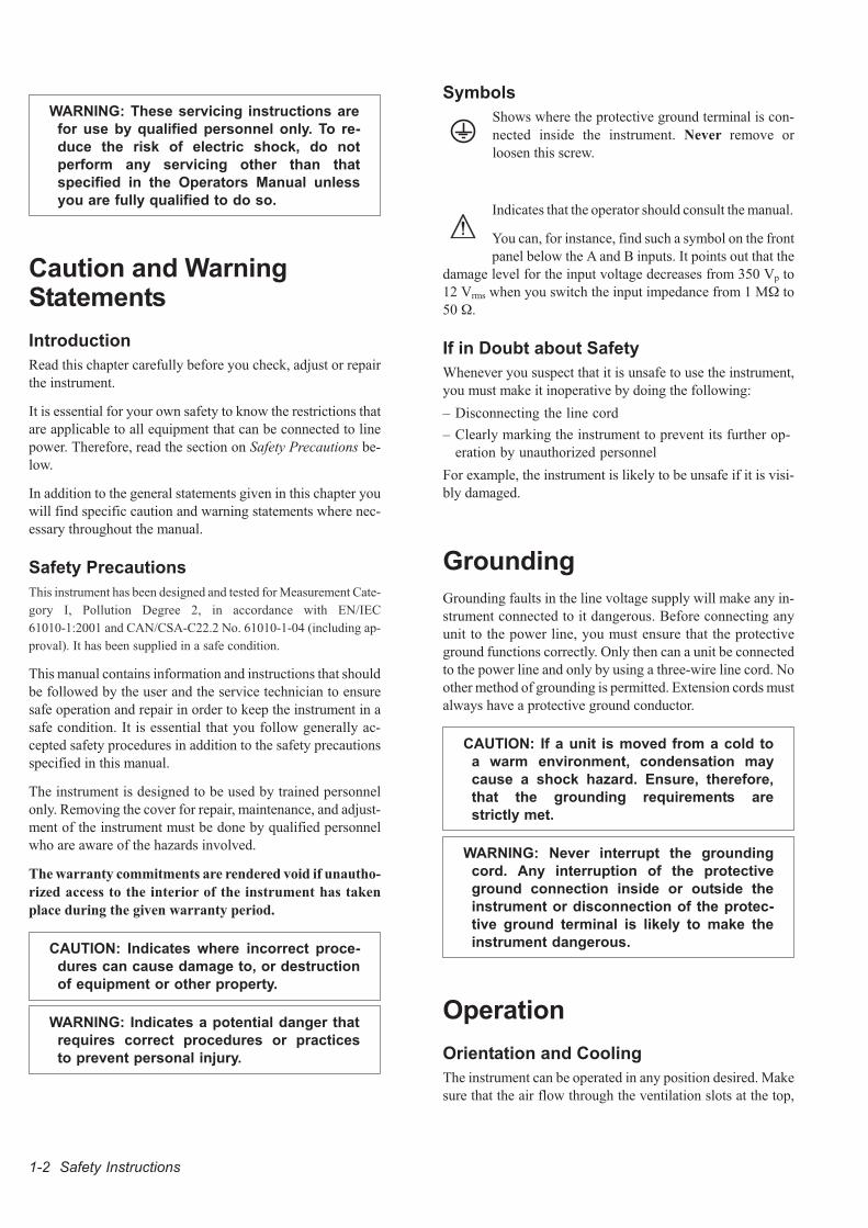
Symbols
Shows where the protective ground terminal is con-
nected inside the instrument. Never remove or
loosen this screw.
Indicates that the operator should consult the manual.
You can, for instance, find such a symbol on the front
panel below the A and B inputs. It points out that the
damage level for the input voltage decreases from 350 Vp to
12 Vrms when you switch the input impedance from 1 M� to
50 �.
If in Doubt about Safety
Whenever you suspect that it is unsafe to use the instrument,
you must make it inoperative by doing the following:
– Disconnecting the line cord
– Clearly marking the instrument to prevent its further op-
eration by unauthorized personnel
For example, the instrument is likely to be unsafe if it is visi-
bly damaged.
Grounding
Grounding faults in the line voltage supply will make any in-
strument connected to it dangerous. Before connecting any
unit to the power line, you must ensure that the protective
ground functions correctly. Only then can a unit be connected
to the power line and only by using a three-wire line cord. No
other method of grounding is permitted. Extension cords must
always have a protective ground conductor.
CAUTION: If a unit is moved from a cold to
a warm environment, condensation may
cause a shock hazard. Ensure, therefore,
that the grounding requirements are
strictly met.
WARNING: Never interrupt the grounding
cord. Any interruption of the protective
ground connection inside or outside the
instrument or disconnection of the protec-
tive ground terminal is likely to make the
instrument dangerous.
Operation
Orientation and Cooling
The instrument can be operated in any position desired. Make
sure that the air flow through the ventilation slots at the top,
1-2 Safety Instructions
and side panels is not obstructed. Leave 5 centimeters (2
inches) of space around the counter.
Fold-Down Support
For bench-top use, a fold-down support is available for use
underneath the counter. This support can also be used as a
handle to carry the instrument.
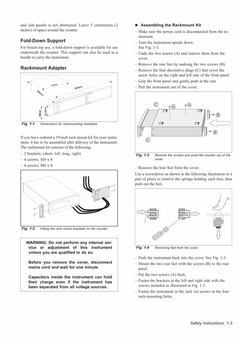
Rackmount Adapter
If you have ordered a 19-inch rack-mount kit for your instru-
ment, it has to be assembled after delivery of the instrument.
The rackmount kit consists of the following:
– 2 brackets, (short, left; long, right)
– 4 screws, M5 x 8
– 4 screws, M6 x 8
WARNING: Do not perform any internal ser-
vice or adjustment of this instrument
unless you are qualified to do so.
Before you remove the cover, disconnect
mains cord and wait for one minute.
Capacitors inside the instrument can hold
their charge even if the instrument has
been separated from all voltage sources.
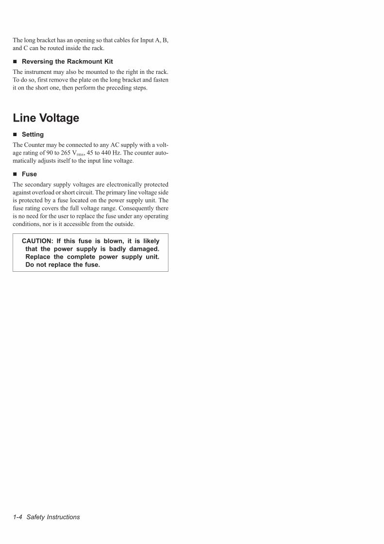
� Assembling the Rackmount Kit
– Make sure the power cord is disconnected from the in-
strument.
– Turn the instrument upside down.
See Fig. 1-3.
– Undo the two screws (A) and remove them from the
cover.
– Remove the rear feet by undoing the two screws (B).
– Remove the four decorative plugs (C) that cover the
screw holes on the right and left side of the front panel.
– Grip the front panel and gently push at the rear.
– Pull the instrument out of the cover.
– Remove the four feet from the cover.
Use a screwdriver as shown in the following illustration or a
pair of pliers to remove the springs holding each foot, then
push out the feet.
– Push the instrument back into the cover. See Fig. 1-3.
– Mount the two rear feet with the screws (B) to the rear
panel.
– Put the two screws (A) back.
– Fasten the brackets at the left and right side with the
screws included as illustrated in Fig. 1-1.
– Fasten the instrument in the rack via screws in the four
rack-mounting holes
Safety Instructions 1-3
Fig. 1-1 Dimensions for rackmounting hardware.
Fig. 1-2 Fitting the rack mount brackets on the counter.
Fig. 1-3 Remove the screws and push the counter out of the
cover.
Fig. 1-4 Removing feet from the cover.
The long bracket has an opening so that cables for Input A, B,
and C can be routed inside the rack.
� Reversing the Rackmount Kit
The instrument may also be mounted to the right in the rack.
To do so, first remove the plate on the long bracket and fasten
it on the short one, then perform the preceding steps.
Line Voltage
� Setting
The Counter may be connected to any AC supply with a volt-
age rating of 90 to 265 Vrms, 45 to 440 Hz. The counter auto-
matically adjusts itself to the input line voltage.
� Fuse
The secondary supply voltages are electronically protected
against overload or short circuit. The primary line voltage side
is protected by a fuse located on the power supply unit. The
fuse rating covers the full voltage range. Consequently there
is no need for the user to replace the fuse under any operating
conditions, nor is it accessible from the outside.
CAUTION: If this fuse is blown, it is likely
that the power supply is badly damaged.
Replace the complete power supply unit.
Do not replace the fuse.
1-4 Safety Instructions

Chapter 2
Performance Check
General Information
WARNING: Before turning on the instru-
ment, ensure that it has been installed in
accordance with the Installation Instruc-
tions outlined in Chapter 1 of the
Operators Manual.
This performance procedure is intended for:
– checking the instrument’s specification.
– incoming inspection to determine the acceptability of
newly purchased instruments and recently recalibrated
instruments.
– checking the necessity of recalibration after the specified
recalibration intervals.
NOTE: The procedure does not check every facet of the in-
strument’s calibration; rather, it is concerned primarily
with those parts of the instrument which are essential
for determining the function of the instrument.
It is not necessary to remove the instrument cover to perform
this procedure.
Test Equipment
Preparations
Power up your instrument at least 30 minutes
before checking to let it reach normal operating
temperature. Failure to do so may result in cer-
tain test steps not meeting equipment specifications.
Front Panel Controls
Internal Self-Tests
The test programs forming the self-diagnosis can be activated
from the front panel as follows:
– Press USER OPT
– Press Test.
– Press Test Mode.
– Select one of the six tests available by pressing the
softkey below the label with the name of the test func-
tion. Five of the tests (RAM, ROM, Logic, Display, and
Interface) are individual. They are briefly described be-
low. The sixth, named All, performs all five individual
tests in sequence.
• All - all tests performed in sequence
• RAM - test of RAM memory
• ROM - test of ROM memory
• Logic - test of counter ASIC and other logic circuits.
• Display - test of graphic displaymodule
• Interface - test of GPIB and USB
– Press Start Test.
– If a fault is detected, an error message appears on the
display and the program halts. Note any error messages.
– If no faults are detected, the instrument returns to the
normal measurement mode.
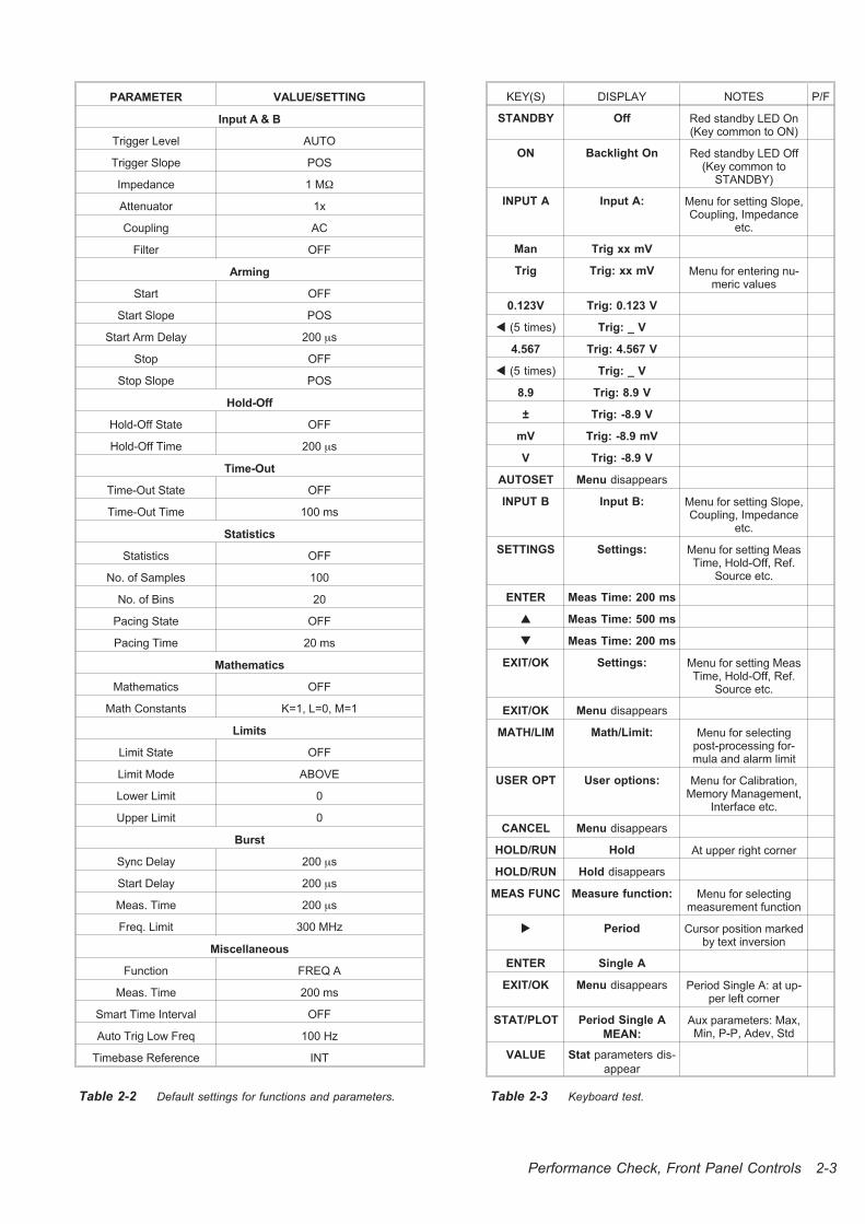
Keyboard Test
See Table 2-3. This test verifies that the timer/counter re-
sponds when you press any key. It is not a functional test.
Such tests are performed later in this chapter. The important
thing here is that something changes on the display when you
press a key. Consequently you can press the keys in almost
any order without paying attention to the exact response, but
for those who want to be more systematic there is a table over-
leaf, where all keys are exercised at least once.
Press the keys as described in the first column and look at the
display for the text in the second column. Some keys change
more text on the display than described here. The display text
mentioned here is the one mostly associated with the selected
key.
NOTE: For the instrument to respond correctly, this test
must be carried out in sequence and you must start
with the DEFAULT setting. Do as follows:
– Press USER OPT.– Press Save/Recall.– Press Recall Setup.– Press Default.
See Table 2-2 for the complete list of default settings.
2-2 Performance Check, General Information
Type of Equipment Required Specifications
Reference Oscillator
10 MHz, 1*10–8
(e.g. 908) for calibrat-ing PM6690/_1_
10 MHz, 1*10–9
(e.g. 909) for calibrat-ing PM6690/_5_ & PM6690/_6_
Voltage Calibrator
DC -50 V to +50 V (e.g. 5500A) forcalibrating the built-in voltage refer-ence, alternatively corresponding DCpower supply + DVM with uncertainty<0.1 %
LF Synthesizer Square/ Sine up to 10 MHz, 10 VRMS
Pulse Generator2 ns rise time, 5 V peak, >10 MHz,continuous & one-shot trigger
Oscilloscope 350 MHz, <3% voltage uncertainty
RF Signal Generator10 MHz to 3 or 8 GHz dep. onprescaler option, 10 MHz ext.ref.
Power Splitter 50 � 6 dB BNC
T Adapter (F-M-F) BNC
Termination 50 � feedthrough BNC
Lowpass Filter 50 kHz (for 1 M� load)
BNC Cables 5 to 7 pcs of suitable lengths
Table 2-1 Recommended equipment for calibration and per-
formance check.
Performance Check, Front Panel Controls 2-3
PARAMETER VALUE/SETTING
Input A & B
Trigger Level AUTO
Trigger Slope POS
Impedance 1 M�
Attenuator 1x
Coupling AC
Filter OFF
Arming
Start OFF
Start Slope POS
Start Arm Delay 200 �s
Stop OFF
Stop Slope POS
Hold-Off
Hold-Off State OFF
Hold-Off Time 200 �s
Time-Out
Time-Out State OFF
Time-Out Time 100 ms
Statistics
Statistics OFF
No. of Samples 100
No. of Bins 20
Pacing State OFF
Pacing Time 20 ms
Mathematics
Mathematics OFF
Math Constants K=1, L=0, M=1
Limits
Limit State OFF
Limit Mode ABOVE
Lower Limit 0
Upper Limit 0
Burst
Sync Delay 200 �s
Start Delay 200 �s
Meas. Time 200 �s
Freq. Limit 300 MHz
Miscellaneous
Function FREQ A
Meas. Time 200 ms
Smart Time Interval OFF
Auto Trig Low Freq 100 Hz
Timebase Reference INT
Table 2-2 Default settings for functions and parameters.
KEY(S) DISPLAY NOTES P/F
STANDBY Off Red standby LED On(Key common to ON)
ON Backlight On Red standby LED Off(Key common to
STANDBY)
INPUT A Input A: Menu for setting Slope,Coupling, Impedance
etc.
Man Trig xx mV
Trig Trig: xx mV Menu for entering nu-meric values
0.123V Trig: 0.123 V
� (5 times) Trig: _ V
4.567 Trig: 4.567 V
� (5 times) Trig: _ V
8.9 Trig: 8.9 V
± Trig: -8.9 V
mV Trig: -8.9 mV
V Trig: -8.9 V
AUTOSET Menu disappears
INPUT B Input B: Menu for setting Slope,Coupling, Impedance
etc.
SETTINGS Settings: Menu for setting MeasTime, Hold-Off, Ref.
Source etc.
ENTER Meas Time: 200 ms
� Meas Time: 500 ms
� Meas Time: 200 ms
EXIT/OK Settings: Menu for setting MeasTime, Hold-Off, Ref.
Source etc.
EXIT/OK Menu disappears
MATH/LIM Math/Limit: Menu for selectingpost-processing for-mula and alarm limit
USER OPT User options: Menu for Calibration,Memory Management,
Interface etc.
CANCEL Menu disappears
HOLD/RUN Hold At upper right corner
HOLD/RUN Hold disappears
MEAS FUNC Measure function: Menu for selectingmeasurement function
� Period Cursor position markedby text inversion
ENTER Single A
EXIT/OK Menu disappears Period Single A: at up-per left corner
STAT/PLOT Period Single A
MEAN:
Aux parameters: Max,Min, P-P, Adev, Std
VALUE Stat parameters dis-
appear
Table 2-3 Keyboard test.
Short Form SpecificationTest
Sensitivity and Frequency Range
– Recall the DEFAULT settings.
– Press INPUT A.
– Select 50 � input impedance, 1x attenuation, MANual
trigger and Trigger level 0 V.
– Connect a signal from a HF generator to a BNC power
splitter.
– Connect the power splitter to Input A of your counter
and an oscilloscope.
– Set the input impedance to 50 � on the oscilloscope.
– Adjust the amplitude according to the following table.
Read the level on the oscilloscope. The timer/counter
should display the correct frequency.
– Connect the signal to Input B.
– Press INPUT B.
– Select 50 � input impedance, 1x attenuation, MANual
trigger and Trigger level 0 V.
– Press MEAS FUNC � Freq � Freq A �B
– Repeat the measurements above for Input B.
Voltage
– Recall the DEFAULT settings.
– Press MEAS FUNC � Volt � Vpp � A
– Press INPUT A and select DC coupling. Do not apply an
input signal to Input A yet.
– Press EXIT/OK.
– The display should now indicate
(disregard the main parameter VPP):
VMIN = 0 ± 0.015 V and
VMAX = 0 ± 0.015 V
– Adjust the current limit of the voltage source to
<200 mA.
– Connect +2.500 VDC to Channel A, using the external
low-pass filter on the input.
– The display should now indicate:
VMIN = 2.500 ± 0.040 V and
VMAX = 2.500 ± 0.040 V
– Repeat the measurement with inverted polarity.
– Press INPUT A and select 10x.
– Press EXIT/OK.
CAUTION: Before the next step, make sure
the input impedance is still 1 M�. Apply-
ing more than 12 V without proper current
limiting may cause extensive damage to
the main PCB, if the impedance is set to
50 �.
– Change the DC level to +50.00 V.
– The display should now indicate:
VMIN = 50.00 ± 0.65 V and
VMAX = 50.00 ± 0.65 V
– Repeat the measurement with inverted polarity.
– Disconnect the DC voltage from Channel A.
– Remove the external low-pass filter.
– Press INPUT A and select 1x.
– Press EXIT/OK.
– Connect a sinusoidal signal to Input A with an amplitude
of 4.000 Vpp and a frequency of 100 kHz.
– The display should now indicate: 4.000 ± 0.150 VPP.
– Press INPUT A and select 10x.
– Press EXIT/OK.
– Change the amplitude to 18.00 VPP.
– The display should now indicate:
18.00 ± 0.84 VPP.
– Disconnect the signal from Channel A.
– Press MEAS FUNC � Volt � Vpp �B
– Press INPUT B and select DC coupling. Do not apply an
input signal to Input B yet.
– Press EXIT/OK.
– The display should now indicate
(disregard the main parameter VPP):
VMIN = 0 ± 0.015 V and
VMAX = 0 ± 0.015 V
– Proceed by repeating the measurements for Input B as
described above for Input A.
Trigger Indicators vs. Trigger Levels
NOTE: This test must be performed in the sequence given.
– Recall the DEFAULT settings.
2-4 Performance Check, Short Form Specification Test
Trigger Level
(manually set)
Trigger Indicator Pass
Input A Input B
+1 V off
-1 V on
0.0 V blinking
Table 2-4 Trigger indicator check.
Frequency
(MHz)
Level Pass/Fail
mVrms dBm Input A Input B
10 15 –23
50 15 –23
100 15 –23
200 15 –23
300 25 –19
Table 2-5 Sensitivity for inputs A & B at various frequencies
– Press INPUT A and select MANual trigger level and 50 �
input impedance.
– Connect the LF synthesizer to Input A. Use the follow-
ing settings (into 50 �):
Sine, 10 kHz, 0.9 VPP, and +0.50 VDC.
– Verify that the three modes for the trigger indicator are
working properly by changing the trigger level:– Press the Trig key and enter +1 V via the keyboard,
then verify by pressing EXIT/OK. Check the triggerindicator according to Table 2-4.
– Press the Trig key and enter –1 V via the keyboardby pressing the ± key, then verify by pressingEXIT/OK. Check the trigger indicator according toTable 2-4.
– Press the Trig key and enter 0 via the keyboard, thenverify by pressing EXIT/OK. Check the trigger indica-tor according to Table 2-4.
– Apply the signal to Input B instead.
– Press MEAS FUNC � Freq � Freq (A) � B
– Press INPUT B and select MANual trigger level and
50 � input impedance..
– Repeat the trigger level settings above to verify the three
trigger indicator modes for Input B.
Input Controls
– Recall the DEFAULT settings.
– Connect the LF synthesizer to Input A. Use the same
settings as in the previous test.
– Press INPUT A and select DC and 50 �.
– Press EXIT/OK.
– Check the Vmax and Vmin voltage levels on the display
according to the first row in Table 2-6.
– Perform the rest of the settings in sequence, and read the
corresponding Vmax and Vmin values. Remember that all
these values are approximate and serve only as indica-
tors of state changes.
– Connect the generator to Input B.
– Press MEAS FUNC � Freq � Freq (A) � B
– Press INPUT B and select DC and 50 �.
– Press EXIT/OK.
– Check the Vmax and Vmin voltage levels on the display
according to the first row in Table 2-6.
– Perform the rest of the settings in sequence, and read the
corresponding Vmax and Vmin values.
Reference Oscillators
X-tal oscillators are affected by a number of external condi-
tions like ambient temperature and supply voltage. Aging is
also an important factor. Therefore it is hard to give limits for
the allowed frequency deviation. The user himself must de-
cide the limits depending on his application, and recalibrate
the oscillator accordingly.
To check the accuracy of the oscillator you must have a cali-
brated reference signal that is at least five times more stable
than the oscillator that you are testing. See Table 2-7 and the
list of test equipment on page 2-2. If you use a non-10 MHz
reference, you can use the mathematics in the timer/counter to
multiply the reading.
– Recall the DEFAULT settings. See page 2-2
– Connect the reference to input A
– Check the readout against the accuracy requirements of
your application.
� Acceptance Test
Table 2-7 can serve as an acceptance test and gives a worst
case figure after 30 minutes warm-up time. All deviations that
can occur in a year are added together.
Resolution Test
– Connect the pulse generator to a power splitter.
– Connect one side of the power splitter to Input A on the
counter using a coaxial cable.
– Connect the other side of the power splitter to Input B
on the counter.
Settings for the pulse generator:
– Amplitude = 2 VPP, (high level +2V and low level 0 V)
– Period = approx. 1 �s
– Duration = approx. 50 ns
– Rise time = 2 ns
Restore the timer/counter's default settings and make the fol-
lowing changes:
– Function = Time A-B
– Press STAT/PLOT key to the right of the display.
– Settings for INPUT A and INPUT B:
50 � input impedance
MANual trigger level
Performance Check, Short Form Specification Test 2-5
Settings Vmax Vmin Pass/Fail
Input A Input B
INPUT A, DC, 50 � +950 mV +50 mV
AC +450 mV -450 mV
10X +0.45 V -0.45 V
1 M� >+0.45 V <-0.45 V
Table 2-6 Input controls check.
Oscillator Frequency Readout Suitable
Reference
P/F
Standard(PM6690/_1_)
10.00000000 MHz � 150 Hz 908
OCXO(PM6690/_5_)
10.00000000 MHz � 1 Hz 909
OCXO(PM6690/_6_)
10.00000000 MHz � 0.25 Hz 909
Table 2-7 Acceptance test for oscillators.
Trig level = 0.5V
DC coupling
The standard deviation (Std) should be <100 ps.
Rear Inputs/Outputs
10 MHz OUT
– Connect an oscilloscope to the 10 MHz output on the
rear of the counter. Use a coaxial cable and 50 � termi-
nation.
– The output voltage should be sinusoidal and above 1
VRMS (2.8 Vp-p).
EXT REF FREQ INPUT
– Recall the DEFAULT settings.
– Connect a stable 10 MHz signal (e.g REF OUT from an-
other counter) to input A.
– Connect a 10 MHz, 100 mVRMS, (0.28 VP-P) signal from
the LF synthesizer to EXT REF IN.
– Select Ext Ref. by keying in the following sequence:
SETTINGS � Timebase Ref � Ext
– The display should show 10 MHz.
– Change the external reference frequency to 5 and
1 MHz.
– The counting should continue, and the display should
still show 10 MHz.
EXT ARM INPUT
– Proceed from the test above.
– Select MANual trigger.
– Settings for the pulse generator:
single shot pulse, manual trigger,
amplitude TTL = 0 - 2 VPP, and
duration = 10 ns.
– Connect the pulse generator to Ext Arm Input.
– Activate start arming by keying in the following se-
quence:
SETTINGS � Start Chan � E
– The counter does not measure.
– Apply one single pulse to Ext Arm Input.
– The counter measures once and shows 10 MHz on the
display.
Measuring Functions
– Connect a 10 MHz sine wave signal with approx.
1 VRMS amplitude into 50 � via a power splitter to Input
A and Input B, e.g. from 10 MHz Out on the rear panel.
– Recall the DEFAULT settings.
Select the following settings for the timer/counter via INPUT
A and INPUT B:
– 50 � impedance for A and B.
– MANual trigger.
2-6 Performance Check, Rear Inputs/Outputs
Selected Function Action Display P/F
FREQ A 10 MHz 2)
FREQ B 10 MHz 2)
FREQ C - - - - - - - - - - - - - - 3)
FREQ RATIO A/B 1.0000000
FREQ RATIO C/B 0.0000000 3)
PER SINGLE A 100 ns 2)
PER SINGLE B 100 ns 2)
PER AVERAGE A 100 ns 2)
PER AVERAGE B 100 ns 2)
PULSE POS A 50.000 ns 1)
PULSE NEG A 50.000 ns 1)
TIME INT A to B 0 ± 1 ns
Select NEGSLOPE B
50.000 ns 1)
RISE TIME A Select AUTOtrigger
30.000 ns 2)
FALL TIME A 30.000 ns 2)
PHASE A rel B 180° or -180° 1)
PHASE B rel A 180° or -180° 1)
PHASE A rel A 0°
DUTY POS A 0.500000 1)
DUTY NEG A 0.500000 1)
VOLT MAX A +0.75 V 2)
VOLT MIN A -0.75 V 2)
Table 2-8 Measuring functions check
1) Value depends on the symmetry of the signal.
2) Exact value depends on input signal.
3) If an RF option is installed.
– Check that the timer/counter performs the correct mea-
surement by displaying the result as shown under the
“Display” column in Table 2-8.
– Select function via MEAS FUNC
Check of HOLD OFFFunction
– Recall the DEFAULT settings.
– Select Period Single A.
Select the following common timer/counter settings for both
Input A and Input B via the hard menu keys INPUT A and IN-
PUT B:
– 50 � impedance.
– DC coupling.
– MANual trigger, x1 attenuation.
– Press SETTINGS and activate Hold Off. Select Hold Off
On and set the Trigger Hold Off time to the minimum
value 20 ns.
– Connect the rear panel output marked 10 MHz OUT to
Input A.
– Increase the Trigger Hold Off time in steps by means of
the UP cursor key and note the results:
If Trigger Hold Off time <100 ns the result is about 100 ns,
i.e. the same value as without Hold Off.
If Trigger Hold Off time >100 ns the result is about 100 ns +
Trig Hold Off time.
– Connect the signal to Input B, select
Period Single B and repeat the tests above.
RF Options
Input C Check
To verify the specification of the different RF prescalers
(Input C), use the following basic test setup:
– Connect the output of a signal generator covering the
specified frequency range to the RF input of the counter.
– Connect the 10 MHz REF OUT from the generator to
the EXT REF IN on the rear panel of the counter.
– Choose Meas Ref from the SETTINGS menu and select
External.
– Choose Freq C from the MEAS FUNC menu.
– Generate a sine wave in accordance with the tables.
– Verify that the counter is counting correctly. (The last
digits will be unstable)
Performance Check, Check of HOLD OFF Function 2-7
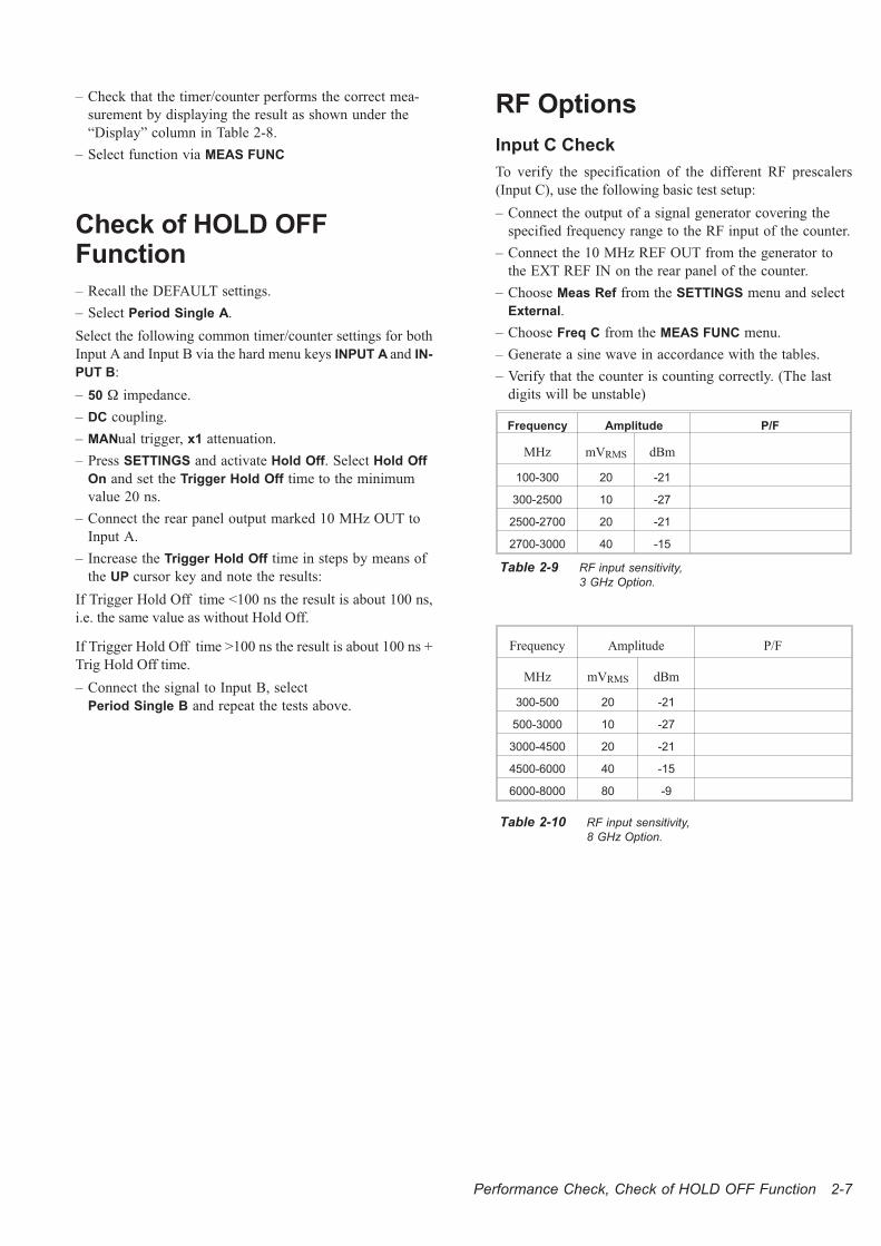
Frequency Amplitude P/F
MHz mVRMS dBm
100-300 20 -21
300-2500 10 -27
2500-2700 20 -21
2700-3000 40 -15
Table 2-9 RF input sensitivity,
3 GHz Option.
Frequency Amplitude P/F
MHz mVRMS dBm
300-500 20 -21
500-3000 10 -27
3000-4500 20 -21
4500-6000 40 -15
6000-8000 80 -9
Table 2-10 RF input sensitivity,
8 GHz Option.

This page is intentionally left blank.
2-8 Performance Check, RF Options

Chapter 3
Disassembly
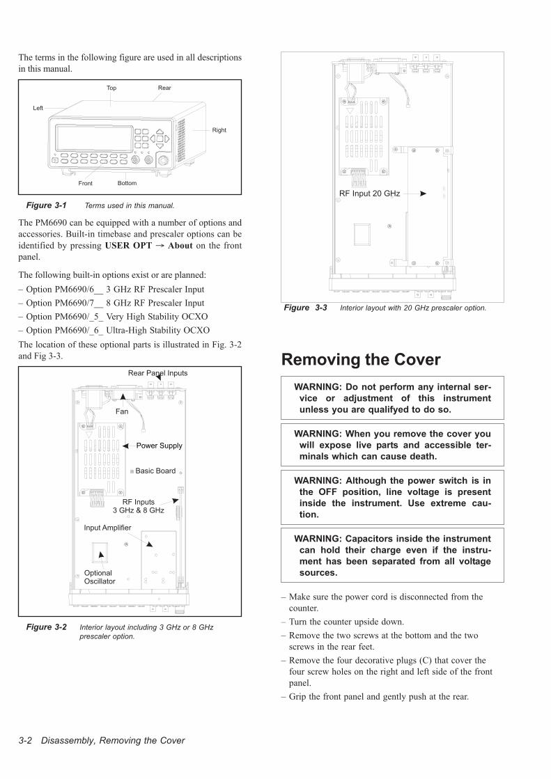
The terms in the following figure are used in all descriptions
in this manual.
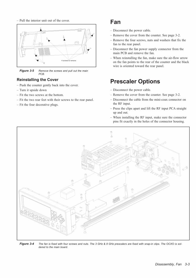
The PM6690 can be equipped with a number of options and
accessories. Built-in timebase and prescaler options can be
identified by pressing USER OPT � About on the front
panel.
The following built-in options exist or are planned:
– Option PM6690/6__ 3 GHz RF Prescaler Input
– Option PM6690/7__ 8 GHz RF Prescaler Input
– Option PM6690/_5_ Very High Stability OCXO
– Option PM6690/_6_ Ultra-High Stability OCXO
The location of these optional parts is illustrated in Fig. 3-2
and Fig 3-3. Removing the Cover
WARNING: Do not perform any internal ser-
vice or adjustment of this instrument
unless you are qualifyed to do so.
WARNING: When you remove the cover you
will expose live parts and accessible ter-
minals which can cause death.
WARNING: Although the power switch is in
the OFF position, line voltage is present
inside the instrument. Use extreme cau-
tion.
WARNING: Capacitors inside the instrument
can hold their charge even if the instru-
ment has been separated from all voltage
sources.
– Make sure the power cord is disconnected from the
counter.
– Turn the counter upside down.
– Remove the two screws at the bottom and the two
screws in the rear feet.
– Remove the four decorative plugs (C) that cover the
four screw holes on the right and left side of the front
panel.
– Grip the front panel and gently push at the rear.
3-2 Disassembly, Removing the Cover
Front Bottom
Right
RearTop
Left
Figure 3-1 Terms used in this manual.
Rear Panel Inputs
Basic Board
Power Supply
RF Inputs3 GHz & 8 GHz
Input Amplifier
OptionalOscillator
Fan
Figure 3-2 Interior layout including 3 GHz or 8 GHz
prescaler option.
RF Input 20 GHz
Figure 3-3 Interior layout with 20 GHz prescaler option.
– Pull the interior unit out of the cover.
Reinstalling the Cover
– Push the counter gently back into the cover.
– Turn it upside down
– Fit the two screws at the bottom.
– Fit the two rear feet with their screws to the rear panel.
– Fit the four decorative plugs.
Fan
– Disconnect the power cable.
– Remove the cover from the counter. See page 3-2.
– Remove the four screws, nuts and washers that fix the
fan to the rear panel.
– Disconnect the fan power supply connector from the
main PCB and remove the fan.
– When reinstalling the fan, make sure the air-flow arrow
on the fan points to the rear of the counter and the black
wire is oriented toward the rear panel.
Prescaler Options
– Disconnect the power cable.
– Remove the cover from the counter. See page 3-2.
– Disconnect the cable from the mini-coax connector on
the RF input.
– Press the clips apart and lift the RF input PCA straight
up and out.
– When installing the RF input, make sure the connector
pins fit exactly in the holes of the connector housing.
Disassembly, Fan 3-3
Figure 3-4 The fan is fixed with four screws and nuts. The 3 GHz & 8 GHz prescalers are fixed with snap-in clips. The OCXO is sol-
dered to the main board.
4 screws to remove
C
Figure 3-5 Remove the screws and pull out the main
PCB.
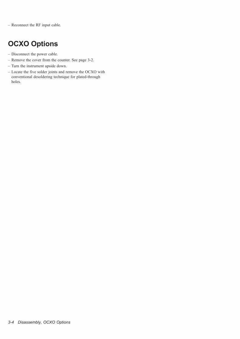
– Reconnect the RF input cable.
OCXO Options
– Disconnect the power cable.
– Remove the cover from the counter. See page 3-2.
– Turn the instrument upside down.
– Locate the five solder joints and remove the OCXO with
conventional desoldering technique for plated-through
holes.
3-4 Disassembly, OCXO Options

Chapter 4
Circuit Descriptions

This page is intentionally left blank.
4-2

Version A
The descriptions in this section apply to instru-
ments having a Triscend microprocessor.
See General Information on page III for details on
relevant serial numbers etc.
Version A 4-3

Block Diagram Description
General
The PM6690 Timer/Counter consists of three main units:
– Front unit
– Main printed circuit board
– Rear panel unit
Several options exist:
– Prescalers on separate PCBs covering different fre-
quency ranges (3 GHz and 8 GHz)
– Two OCXO timebases (very high & ultra-high stability)
– Rackmount kit
The chassis of the counter consists of a front piece molded in
aluminum, an aluminum rear panel, and two extruded alumi-
num bars that hold the front and rear panels together. This unit
can be slid into the aluminum cover of the instrument.
The main circuit board is fixed to the two bars. The display
circuit board is fixed to the front piece. A detachable connec-
tor joins the electronics of the front unit and the main board,
and the molded front piece is fixed with screws to the two alu-
minum bars. The rear panel is also fixed to the bars with
screws.
The front unit contains all functions needed for the user com-
munication: keyboard, display and input BNCs. All other
electrical functions are on the main board. The rear panel has
no PCB. The connectors here are all soldered directly to the
main circuit board.
Block Diagram
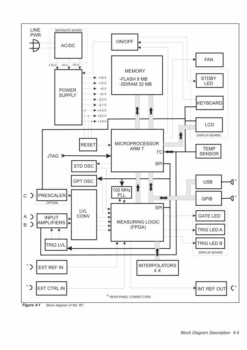
Figure 4-1 contains a block diagram of the electrical functions
of the counter. They are divided among the main circuit board,
the display board, the rear panel and the optional prescaler
board. See the schematic diagrams in Chapter 9 for complete
information.
Most functions are placed on the main board:
– Input amplifiers with trigger level circuits
– Power supply
– Measurement logic
– Microcomputer circuitry
– GPIB interface
– USB interface
– External reference input
– External arming input
The rear panel unit is made of aluminum with a number of
mounted connectors, a fan and a power line inlet with filter.
Most connectors are soldered directly to the main board.
NOTE: Schematic diagrams in this chapter are simplified.
For complete information, see Chapter 9.
4-4 Block Diagram Description
Block Diagram Description 4-5
ON/OFF
RESET MICROPROCESSORARM 7
STD OSC
OPT OSC
100 MHzPLL
FAN
STDBYLED
KEYBOARD
LCD
TEMPSENSOR
USB
GPIB
GATE LED
TRIG LED A
TRIG LED B
INT REF OUT
INTERPOLATORS4 X
EXT CTRL IN
EXT REF IN
TRIG LVL
INPUTAMPLIFIERS
PRESCALER
MEASURING LOGIC(FPGA)
LVLCONV
LINEPWR
AC/DC
SEPARATE BOARD
+15 V -15 V+5 V
POWERSUPPLY
+15 V
+12 V
+5 V
-12 V
-5.2 V
-2.1 V
+3.3 V
+2.5 V
+1.8 V
JTAGI C2
DISPLAY BOARD
SPI
SPI
C
A
B
OPTION
DISPLAY BOARD
**
*
*
*
* REAR PANEL CONNECTORS
-FLASH 8 MB-SDRAM 32 MB
MEMORY
Figure 4-1 Block diagram of the '90'.

Hardware Functional Description
Front Unit
The front unit consists of a front piece in molded aluminum, a
silicon rubber keypad with conducting contact surfaces, a
graphic LCD with LED backlight, and a PCB having etched
gold-plated keyboard contacts and a dedicated LCD power
supply.
Display
The display is a 320*97 pixels graphical LCD with LED
backlight. The LCD controller is part of the processor, and it
sends data and control signals to the drivers in the LCD mod-
ule. Display ON is controlled via the I2C bus and the keyboard
IC. The LCD voltages are generated by a DC/DC converter.
Five different voltages are generated. A control signal from
the processor switches the converter ON/OFF and also sets
the contrast of the display.
The 4 LEDs on the display board are controlled from the mea-
suring logic and the ON/OFF circuit.
Keyboard
The PCB covers the back of the front unit. The keys are laid
out as a crosspoint switch matrix consisting of 25 regular push
buttons plus a special power button. When one of the buttons
is depressed, the dedicated keyboard IC U3 responds by
sending an interrupt to the processor. The processor scans the
keyboard over the I2C bus to find out which button calls for
attention. The power button differs from the others by having
a dual function. In Standby Mode it turns on the ON/OFF cir-
cuit directly, but when the counter is ON, it is read as any other
button. Then the processor turns off the counter. This arrange-
ment is necessary since the processor is inactive in standby
mode.
Main Board
Input Amplifiers
Input amplifiers A and B are identical with >300 MHz band-
width. They are controlled by the processor with relays etc.
The analog input signal is transformed to a digital signal. The
output signals are LVPECL (+2.4 V and +1.2 V approxi-
mately) and fed to the measuring logic.
For a block diagram of the input amplifiers, see Figure 4-2.
� Impedance Selector
This stage selects 1 M� or 50 � input impedance with a relay.
In 50 � mode 11 resistors are used for dissipating the input
power, up to a maximum of 2.9 W (12 Vrms).
� Attenuator
This stage has two parts, a fixed preattenuator (approximate
attenuation ����) and a cascaded relay-operated ��/��� step
attenuator. The variable capacitors are used for adjusting the
frequency response of the attenuators.
� AC/DC
This stage selects AC or DC coupling with a relay.
� Limiter
The voltage limiter protects the impedance converter against
overvoltage. The �5 V applied to the input BNC is divided to
approximately �2.1 V by the attenuator. The limiter clamps
the voltage to approximately �2.8 V.
� Impedance Converter
Split-band technique is used for achieving good frequency re-
sponse over a wide range. The HF signal is fed via an
AC-coupled FET stage. The LF signal (bandwidth DC to ap-
proximately 10 kHz) goes via an operational amplifier. The
signals are added together at the source of the FET. The output
signal from the buffer stage (see below) is fed back to the op-
erational amplifier. A trimmer potentiometer is used for
equalizing the gain in the two signal paths (approximately
�0.9).
� Filter
A lowpass RC filter with an approximate cutoff frequency of
100 kHz can be switched in via a transistor.
� Buffer
Before the signal is fed to the Crossover Switch, it passes a
current-amplifying buffer stage that can drive the following
low impedance stages.
4-6 Hardware Functional Description
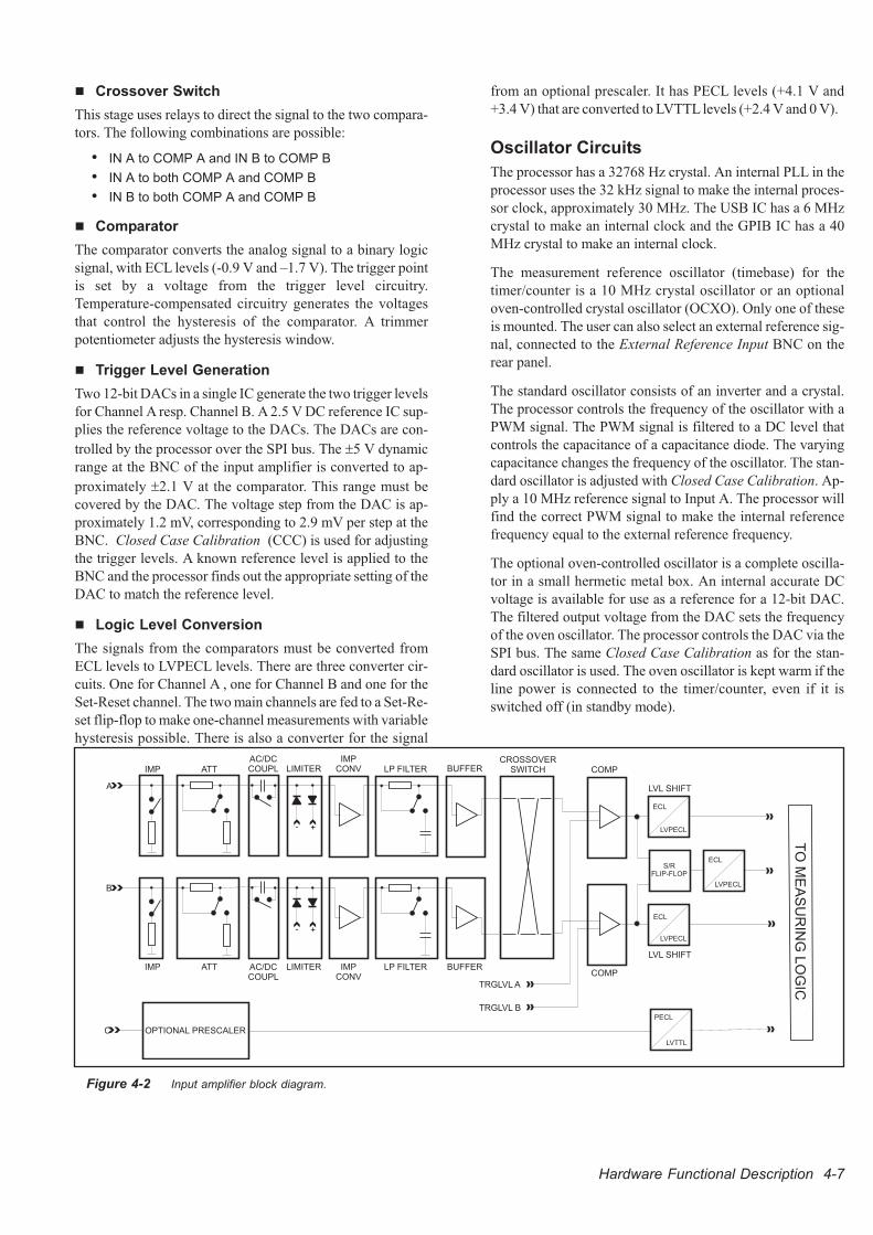
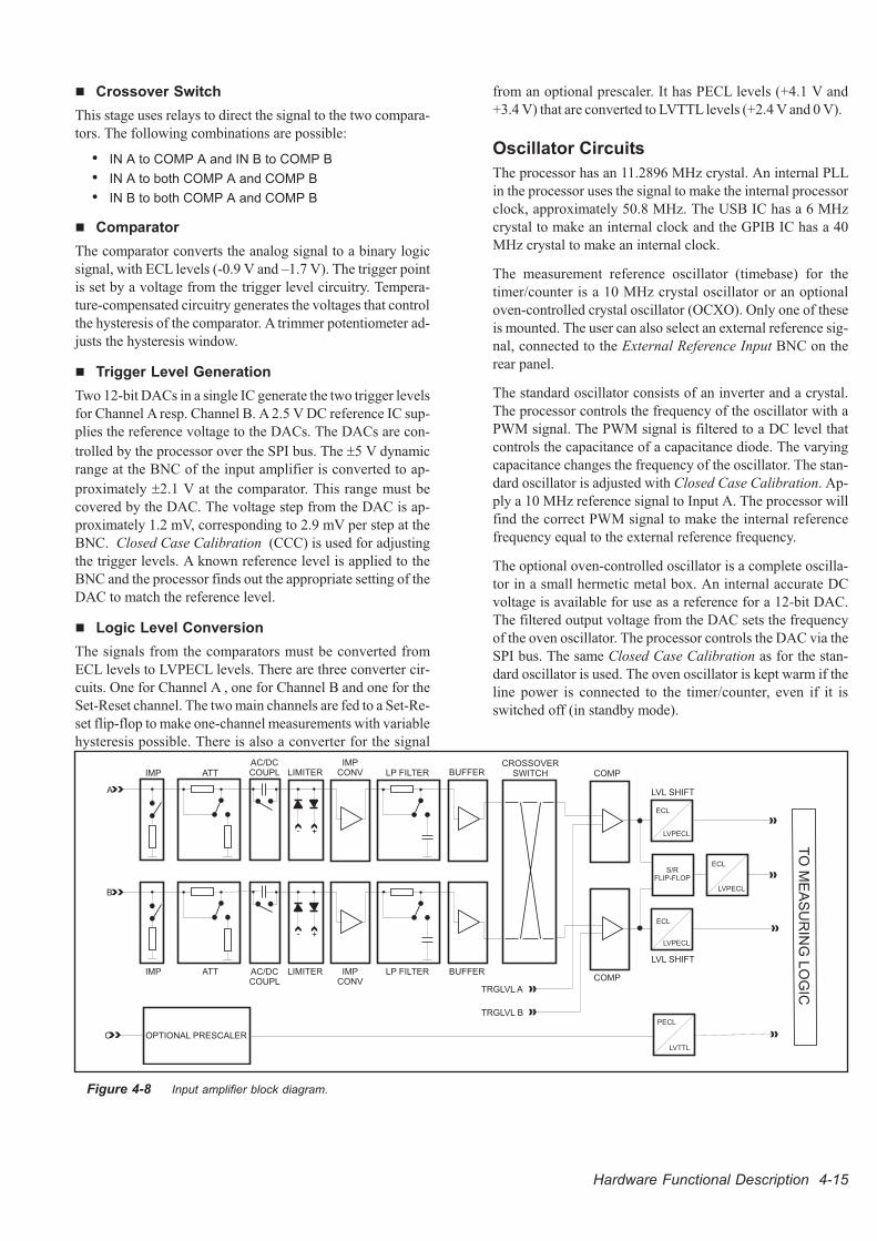
� Crossover Switch
This stage uses relays to direct the signal to the two compara-
tors. The following combinations are possible:
• IN A to COMP A and IN B to COMP B
• IN A to both COMP A and COMP B
• IN B to both COMP A and COMP B
� Comparator
The comparator converts the analog signal to a binary logic
signal, with ECL levels (-0.9 V and –1.7 V). The trigger point
is set by a voltage from the trigger level circuitry.
Temperature-compensated circuitry generates the voltages
that control the hysteresis of the comparator. A trimmer
potentiometer adjusts the hysteresis window.
� Trigger Level Generation
Two 12-bit DACs in a single IC generate the two trigger levels
for Channel A resp. Channel B. A 2.5 V DC reference IC sup-
plies the reference voltage to the DACs. The DACs are con-
trolled by the processor over the SPI bus. The �5 V dynamic
range at the BNC of the input amplifier is converted to ap-
proximately �2.1 V at the comparator. This range must be
covered by the DAC. The voltage step from the DAC is ap-
proximately 1.2 mV, corresponding to 2.9 mV per step at the
BNC. Closed Case Calibration (CCC) is used for adjusting
the trigger levels. A known reference level is applied to the
BNC and the processor finds out the appropriate setting of the
DAC to match the reference level.
� Logic Level Conversion
The signals from the comparators must be converted from
ECL levels to LVPECL levels. There are three converter cir-
cuits. One for Channel A , one for Channel B and one for the
Set-Reset channel. The two main channels are fed to a Set-Re-
set flip-flop to make one-channel measurements with variable
hysteresis possible. There is also a converter for the signal
from an optional prescaler. It has PECL levels (+4.1 V and
+3.4 V) that are converted to LVTTL levels (+2.4 V and 0 V).
Oscillator Circuits
The processor has a 32768 Hz crystal. An internal PLL in the
processor uses the 32 kHz signal to make the internal proces-
sor clock, approximately 30 MHz. The USB IC has a 6 MHz
crystal to make an internal clock and the GPIB IC has a 40
MHz crystal to make an internal clock.
The measurement reference oscillator (timebase) for the
timer/counter is a 10 MHz crystal oscillator or an optional
oven-controlled crystal oscillator (OCXO). Only one of these
is mounted. The user can also select an external reference sig-
nal, connected to the External Reference Input BNC on the
rear panel.
The standard oscillator consists of an inverter and a crystal.
The processor controls the frequency of the oscillator with a
PWM signal. The PWM signal is filtered to a DC level that
controls the capacitance of a capacitance diode. The varying
capacitance changes the frequency of the oscillator. The stan-
dard oscillator is adjusted with Closed Case Calibration. Ap-
ply a 10 MHz reference signal to Input A. The processor will
find the correct PWM signal to make the internal reference
frequency equal to the external reference frequency.
The optional oven-controlled oscillator is a complete oscilla-
tor in a small hermetic metal box. An internal accurate DC
voltage is available for use as a reference for a 12-bit DAC.
The filtered output voltage from the DAC sets the frequency
of the oven oscillator. The processor controls the DAC via the
SPI bus. The same Closed Case Calibration as for the stan-
dard oscillator is used. The oven oscillator is kept warm if the
line power is connected to the timer/counter, even if it is
switched off (in standby mode).
Hardware Functional Description 4-7
AC/DCCOUPLATTIMP LIMITER
- +
IMPCONV LP FILTER BUFFER
CROSSOVERSWITCH
- +
AC/DCCOUPL
ATTIMP LIMITER IMPCONV
LP FILTER BUFFER
LVL SHIFT
ECL
LVPECL
LVL SHIFT
ECL
LVPECL
S/RFLIP-FLOP
ECL
LVPECL
A
B
TRGLVL A
TRGLVL B
OPTIONAL PRESCALER
PECL
LVTTL
C
TO
ME
AS
UR
ING
LO
GIC
Figure 4-2 Input amplifier block diagram.
The 10 MHz reference signal is multiplied in a PLL to
100 MHz. The 100 MHz signal is used in the measuring logic
as a reference. The processor controls the PLL IC with the SPI
bus. A 100 MHz LC oscillator is used as the controlled ele-
ment where part of the C is a variable capacitance diode. Its
capacitance is controlled with a DC voltage from the PLL IC,
thus changing the frequency. The 10 MHz reference signal is
applied to the PLL IC as its reference and the 100 MHz output
frequency is exactly 10 times the reference frequency.
External Reference Input
A 1, 2, 5 or 10 MHz reference signal can be connected to the
rear panel BNC. After amplification in an operational ampli-
fier narrow pulses are made in two D flip-flops, one narrow
pulse for each input cycle. These pulses are fed to the 10 MHz
crystal filter. After the filter a reconstructed 10 MHz signal is
available. A variable capacitor is used for adjusting the filter.
Internal Reference Output
The selected 10 MHz reference signal (standard/oven oscilla-
tor or external reference) is available on the rear panel. The 10
MHz reference signal that is used internally by the dedicated
counter circuit (FPGA) logic is also sent to an output pin on
the FPGA. It is filtered to a sine wave and amplified in an out-
put buffer stage having 50 � drive capability.
Measuring Logic
The measuring logic consists of an FPGA, four interpolators
and an external control input on the rear panel. The FPGA
core uses +1.8 V supply voltage and the I/Os use +3.3 V sup-
ply voltage.
The FPGA is controlled by the processor over a 16-bit micro-
processor bus. Input signals (A, B, prescaler etc) and refer-
ence clock (internal 10 MHz oscillator or external reference)
are selected inside the FPGA. The logic for all measuring
functions and support functions (trigger indicators, start de-
lay, pacing etc) are inside the FPGA. A 100 MHz reference
clock is generated by a PLL circuit giving 10 ns basic mea-
surement resolution. To increase the measurement resolution
further, external interpolators are used. The measuring logic
also controls three LEDs on the display board; a GATE LED
indicating that a measurement is in progress, and two trigger
indicators telling that the comparators are triggering on the in-
put signals. A separate 32-bit bus is used for transferring mea-
surement data from the FPGA to the processor. Some control
signals to the hardware come from the FPGAdue to a shortage
of processor pins.
The four external interpolators are identical. Depending on
the selected measurement function 0, 2, 3 or 4 interpolators
are used. A pulse representing the time from an event on the
input to the following rising edge of the 100 MHz reference is
fed to the interpolator. During the pulse time a constant cur-
rent is charging a capacitor. The voltage on the capacitor is
measured with a 10-bit ADC. The capacitor is discharged and
the interpolator is ready for a new measurement.
An external control input BNC is located on the rear panel. A
signal applied to this connector can be used for controlling the
start of a measurement, for instance. A comparator converts
the analog input signal to a logic signal.
Processor Circuits
The processor is a Triscend A7S. It contains an ARM7 core
and peripherals. It runs on a 30 MHz internal clock. The core
uses 2.5 V supply voltage and the I/Os use 3.3 V supply volt-
age.
A separate memory bus communicates with a 16-bit 8 MByte
flash memory and a 32-bit 32 MByte SDRAM. The flash
memory contains the program, data for loading the FPGA,
and stored data (calibration data etc.). At power-up the code is
copied from the flash to the SDRAM. It is run from the
SDRAM for faster execution.
The processor has a JTAG interface with a connector on the
circuit board.
A reset IC monitors the three main logic supply voltages, +3.3
V, +2.5 V and + 1.8 V. If a supply voltage fails, the processor
will be reset.
The regular 16-bit microprocessor bus is used for controlling
the FPGA, the GPIB interface and the USB interface. A sepa-
rate 32-bit bus is used for fetching measurement data from the
measuring logic.
Two other buses are also used, an SPI bus and an I2C bus. The
SPI bus is an output only bus and the processor controls the
100 MHz PLL, the trigger level DACs, and the DAC for the
optional oven oscillator. The I2C bus is bidirectional and used
for communication with the temperature measurement IC, the
display board (keyboard + LCD), the prescaler (optional), and
the relays and filters in the input amplifier.
The temperature reading over the I2C bus is used for con-
trolling the fan speed. A PWM output is utilized. The signal is
filtered and the resulting DC voltage controls the fan.
Another PWM output is used for controlling the frequency of
the standard crystal oscillator.
The LCD controller is a peripheral inside the processor. This
controller sends signals and data to the driver circuits in the
LCD on the display board.
The processor also controls the OFF switch. Only a signal
from the processor can switch off the power. The OFF button
on the front panel is read by the processor. ON is handled
without the processor, since it cannot respond to external
stimulus in standby mode.
Power Supply
This timer/counter has no primary power switch. If connected
to line power there are live parts inside the cabinet, and some
supply voltages are present on the main circuit board, even if
4-8 Hardware Functional Description
the secondary power switch on the front panel has been turned
off (standby mode).
A semi-protected AC/DC module is placed on spacers over
the main circuit board. It delivers three regulated DC voltages
to the counter, + 15 V, + 5 V and –15 V. When the counter is
connected to line power, these voltages are always present.
There is a + 5 V trimmer potentiometer on the AC/DC mod-
ule.
The ON/OFF circuit is active as soon as the counter is con-
nected to line power. The instrument automatically powers up
when line power is applied. Only the processor can switch the
circuit to OFF state (standby mode). Then only the power but-
ton on the front panel can switch the instrument to ON. Once
connected to line power and in OFF state (standby mode),
supply voltage +12 VU is distributed to the oven oscillator to
keep it warm. In standby mode a red LED is lit on the front
panel. To keep the AC/DC module stable in this mode, a
dummy load is connected to draw a quiescent current of 0.1 A
at +5 V.
The three main voltages are +15 V, +5 V and –15 V from the
AC/DC module. All other supply voltages are generated from
them and are, except for +12 VU to the oven oscillator,
switched off in standby mode.
Linear regulators are used for generating stable voltages with
low noise and without spikes. Some of them have a resistor
net at the input to dissipate part of the heat generated. Thus the
regulator itself will run cooler. The following voltages are
generated in this way:
+3.3 VA from +5 VU
-5.2 VA from -15 VU
-5.2 VI from -12 VA
-2.1 V from -12 VA
-12 VA from -15 VU
+12 VA from +15 VU
+12 VU from + 15 VU, to oven oscillator, not switched off in
standby mode
For digital and general use supply voltages are generated by
DC/DC converters:
+3.3 VD from +5 VU
+5 VD from +5 VU via a switch IC
+15 VD from +15 VU via a switch transistor
+2.5 V from +5 VU
+1.8 V from +5 VU
Communication Interfaces
Both a GPIB and a USB interface are available for communi-
cation with external bus controllers. The connectors are lo-
cated on the rear panel.
The GPIB consists of an IC. Only 8 bits of the 16-bit micro-
processor bus is used. Due to different supply voltages for the
processor (+3.3 V) and the GPIB circuit (+5 V), a buffer IC is
used for isolating the +5 V GPIB IC from the processor bus. A
40 MHz crystal is used for generating a local clock.
The USB consists of an IC. It communicates with the proces-
sor over the 16-bit microprocessor bus. A 6 MHz crystal is
used for generating a local clock.
Rear Panel Unit
The rear panel is made of aluminum. A number of connectors
mounted on this unit are accessible to the user, see Figure 4-3.
I/O:
– GPIB communication connector.
– USB communication connector
INPUTS:
– External reference (BNC)
– External arming (BNC)
– Power supply inlet including EMI filter
Hardware Functional Description 4-9
!
!
!
!
!
!
10 MHz OUT1Vrms IN 50W
EXT REFFREQ INPUT
EXT ARMINPUT E
INPUT A INPUT B INPUT C
GPIB IEEE 488USB
191125
Figure 4-3 Rear panel, PM6690.
– Optional main inputs replacing corresponding front
panel inputs
OUTPUTS:
– Internal reference 10 MHz (BNC)
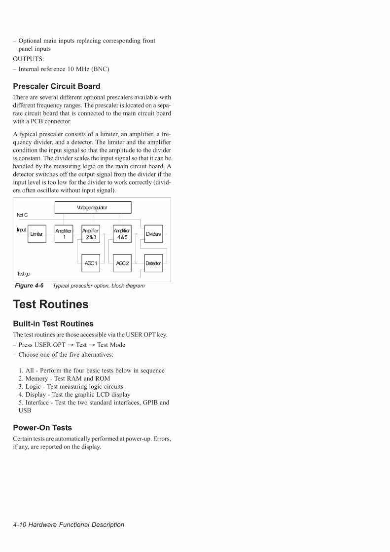
Prescaler Circuit Board
There are several different optional prescalers available with
different frequency ranges. The prescaler is located on a sepa-
rate circuit board that is connected to the main circuit board
with a PCB connector.
A typical prescaler consists of a limiter, an amplifier, a fre-
quency divider, and a detector. The limiter and the amplifier
condition the input signal so that the amplitude to the divider
is constant. The divider scales the input signal so that it can be
handled by the measuring logic on the main circuit board. A
detector switches off the output signal from the divider if the
input level is too low for the divider to work correctly (divid-
ers often oscillate without input signal).
Test Routines
Built-in Test Routines
The test routines are those accessible via the USER OPT key.
– Press USER OPT � Test � Test Mode
– Choose one of the five alternatives:
1. All - Perform the four basic tests below in sequence
2. Memory - Test RAM and ROM
3. Logic - Test measuring logic circuits
4. Display - Test the graphic LCD display
5. Interface - Test the two standard interfaces, GPIB and
USB
Power-On Tests
Certain tests are automatically performed at power-up. Errors,
if any, are reported on the display.
4-10 Hardware Functional Description
LimiterAmplifier
1Amplifier
2&3Amplifier
4&5
AGC1 AGC2
Voltageregulator
Dividers
Detector
Not C
Test go
Input
Figure 4-6 Typical prescaler option, block diagram

Version B
The descriptions in this section apply to instru-
ments having a Sharp microprocessor.
See General Information on page III for details on
relevant serial numbers etc.
Version B 4-11
Block Diagram Description
General
The PM6690 Timer/Counter consists of three main units:
– Front unit
– Main printed circuit board
– Rear panel unit
Several options exist:
– Prescalers on separate PCBs covering different fre-
quency ranges (3 GHz and 8 GHz)
– Two OCXO timebases (very high & ultra-high stability)
– Rackmount kit
The chassis of the counter consists of a front piece molded in
aluminum, an aluminum rear panel, and two extruded alumi-
num bars that hold the front and rear panels together. This unit
can be slid into the aluminum cover of the instrument.
The main circuit board is fixed to the two bars. The display
circuit board is fixed to the front piece. A detachable connec-
tor joins the electronics of the front unit and the main board,
and the molded front piece is fixed with screws to the two alu-
minum bars. The rear panel is also fixed to the bars with
screws.
The front unit contains all functions needed for the user com-
munication: keyboard, display and input BNCs. All other
electrical functions are on the main board. The rear panel has
no PCB. The connectors here are all soldered directly to the
main circuit board.
Block Diagram
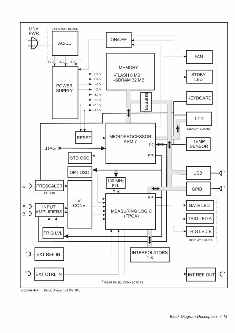
Figure 4-7 contains a block diagram of the electrical functions
of the counter. They are divided among the main circuit board,
the display board, the rear panel and the optional prescaler
board. See the schematic diagrams in Chapter 9 for complete
information.
Most functions are placed on the main board:
– Input amplifiers with trigger level circuits
– Power supply
– Measurement logic
– Microcomputer circuitry
– GPIB interface
– USB interface
– External reference input
– External arming input
The rear panel unit is made of aluminum with a number of
mounted connectors, a fan and a power line inlet with filter.
Most connectors are soldered directly to the main board.
NOTE: Schematic diagrams in this chapter are simplified.
For complete information, see Chapter 9.
4-12 Block Diagram Description
Block Diagram Description 4-13
ON/OFF
RESET MICROPROCESSORARM 7
STD OSC
OPT OSC
100 MHzPLL
-FLASH 8 MB-SDRAM 32 MB
MEMORY
FAN
STDBYLED
KEYBOARD
LCD
TEMPSENSOR
USB
GPIB
GATE LED
TRIG LED A
TRIG LED B
INT REF OUT
INTERPOLATORS4 X
EXT CTRL IN
EXT REF IN
TRIG LVL
INPUTAMPLIFIERS
PRESCALER
MEASURING LOGIC(FPGA)
LVLCONV
LINEPWR
AC/DC
SEPARATE BOARD
+15 V -15 V+5 V
POWERSUPPLY
+15 V
+12 V
+5 V
-12 V
-5.2 V
-2.1 V
+3.3 V
+1.8 V
JTAGI C2
DISPLAY BOARD
SPI
SPI
C
A
B
OPTION
DISPLAY BOARD
**
*
*
*
* REAR PANEL CONNECTORS
BU
FF
ER
Figure 4-7 Block diagram of the '90'.
Hardware Functional Description
Front Unit
The front unit consists of a front piece in molded aluminum, a
silicon rubber keypad with conducting contact surfaces, a
graphic LCD with LED backlight, and a PCB having etched
gold-plated keyboard contacts and a dedicated LCD power
supply.
Display
The display is a 320*97 pixels graphical LCD with LED
backlight. The LCD controller is part of the processor, and it
sends data and control signals to the drivers in the LCD mod-
ule. Display ON is controlled via the I2C bus and the keyboard
IC. The LCD voltages are generated by a DC/DC converter.
Five different voltages are generated. A control signal from
the processor switches the converter ON/OFF and also sets
the contrast of the display.
The 4 LEDs on the display board are controlled from the mea-
suring logic and the ON/OFF circuit.
Keyboard
The PCB covers the back of the front unit. The keys are laid
out as a crosspoint switch matrix consisting of 25 regular push
buttons plus a special power button. When one of the buttons
is depressed, the dedicated keyboard IC U3 responds by send-
ing an interrupt to the processor. The processor scans the key-
board over the I2C bus to find out which button calls for atten-
tion. The power button differs from the others by having a
dual function. In Standby Mode it turns on the ON/OFF circuit
directly, but when the counter is ON, it is read as any other
button. Then the processor turns off the counter. This arrange-
ment is necessary since the processor is inactive in standby
mode.
Main Board
Input Amplifiers
Input amplifiers A and B are identical with >300 MHz band-
width. They are controlled by the processor with relays etc.
The analog input signal is transformed to a digital signal. The
output signals are LVPECL (+2.4 V and +1.2 V approxi-
mately) and fed to the measuring logic.
For a block diagram of the input amplifiers, see Figure 4-8.
� Impedance Selector
This stage selects 1 M� or 50 � input impedance with a relay.
In 50 � mode 11 resistors are used for dissipating the input
power, up to a maximum of 2.9 W (12 Vrms).
� Attenuator
This stage has two parts, a fixed preattenuator (approximate
attenuation ����) and a cascaded relay-operated ��/��� step
attenuator. The variable capacitors are used for adjusting the
frequency response of the attenuators.
� AC/DC
This stage selects AC or DC coupling with a relay.
� Limiter
The voltage limiter protects the impedance converter against
overvoltage. The �5 V applied to the input BNC is divided to
approximately �2.1 V by the attenuator. The limiter clamps
the voltage to approximately �2.8 V.
� Impedance Converter
Split-band technique is used for achieving good frequency re-
sponse over a wide range. The HF signal is fed via an
AC-coupled FET stage. The LF signal (bandwidth DC to ap-
proximately 10 kHz) goes via an operational amplifier. The
signals are added together at the source of the FET. The output
signal from the buffer stage (see below) is fed back to the op-
erational amplifier. A trimmer potentiometer is used for
equalizing the gain in the two signal paths (approximately
�0.9).
� Filter
A lowpass RC filter with an approximate cutoff frequency of
100 kHz can be switched in via a transistor.
� Buffer
Before the signal is fed to the Crossover Switch, it passes a
current-amplifying buffer stage that can drive the following
low impedance stages.
4-14 Hardware Functional Description
� Crossover Switch
This stage uses relays to direct the signal to the two compara-
tors. The following combinations are possible:
• IN A to COMP A and IN B to COMP B
• IN A to both COMP A and COMP B
• IN B to both COMP A and COMP B
� Comparator
The comparator converts the analog signal to a binary logic
signal, with ECL levels (-0.9 V and –1.7 V). The trigger point
is set by a voltage from the trigger level circuitry. Tempera-
ture-compensated circuitry generates the voltages that control
the hysteresis of the comparator. A trimmer potentiometer ad-
justs the hysteresis window.
� Trigger Level Generation
Two 12-bit DACs in a single IC generate the two trigger levels
for Channel A resp. Channel B. A 2.5 V DC reference IC sup-
plies the reference voltage to the DACs. The DACs are con-
trolled by the processor over the SPI bus. The �5 V dynamic
range at the BNC of the input amplifier is converted to ap-
proximately �2.1 V at the comparator. This range must be
covered by the DAC. The voltage step from the DAC is ap-
proximately 1.2 mV, corresponding to 2.9 mV per step at the
BNC. Closed Case Calibration (CCC) is used for adjusting
the trigger levels. A known reference level is applied to the
BNC and the processor finds out the appropriate setting of the
DAC to match the reference level.
� Logic Level Conversion
The signals from the comparators must be converted from
ECL levels to LVPECL levels. There are three converter cir-
cuits. One for Channel A , one for Channel B and one for the
Set-Reset channel. The two main channels are fed to a Set-Re-
set flip-flop to make one-channel measurements with variable
hysteresis possible. There is also a converter for the signal
from an optional prescaler. It has PECL levels (+4.1 V and
+3.4 V) that are converted to LVTTL levels (+2.4 V and 0 V).
Oscillator Circuits
The processor has an 11.2896 MHz crystal. An internal PLL
in the processor uses the signal to make the internal processor
clock, approximately 50.8 MHz. The USB IC has a 6 MHz
crystal to make an internal clock and the GPIB IC has a 40
MHz crystal to make an internal clock.
The measurement reference oscillator (timebase) for the
timer/counter is a 10 MHz crystal oscillator or an optional
oven-controlled crystal oscillator (OCXO). Only one of these
is mounted. The user can also select an external reference sig-
nal, connected to the External Reference Input BNC on the
rear panel.
The standard oscillator consists of an inverter and a crystal.
The processor controls the frequency of the oscillator with a
PWM signal. The PWM signal is filtered to a DC level that
controls the capacitance of a capacitance diode. The varying
capacitance changes the frequency of the oscillator. The stan-
dard oscillator is adjusted with Closed Case Calibration. Ap-
ply a 10 MHz reference signal to Input A. The processor will
find the correct PWM signal to make the internal reference
frequency equal to the external reference frequency.
The optional oven-controlled oscillator is a complete oscilla-
tor in a small hermetic metal box. An internal accurate DC
voltage is available for use as a reference for a 12-bit DAC.
The filtered output voltage from the DAC sets the frequency
of the oven oscillator. The processor controls the DAC via the
SPI bus. The same Closed Case Calibration as for the stan-
dard oscillator is used. The oven oscillator is kept warm if the
line power is connected to the timer/counter, even if it is
switched off (in standby mode).
Hardware Functional Description 4-15
AC/DCCOUPLATTIMP LIMITER
- +
IMPCONV LP FILTER BUFFER
CROSSOVERSWITCH
- +
AC/DCCOUPL
ATTIMP LIMITER IMPCONV
LP FILTER BUFFER
LVL SHIFT
ECL
LVPECL
LVL SHIFT
ECL
LVPECL
S/RFLIP-FLOP
ECL
LVPECL
A
B
TRGLVL A
TRGLVL B
OPTIONAL PRESCALER
PECL
LVTTL
C
TO
ME
AS
UR
ING
LO
GIC
Figure 4-8 Input amplifier block diagram.
The 10 MHz reference signal is multiplied in a PLL to
100 MHz. The 100 MHz signal is used in the measuring logic
as a reference. The processor controls the PLL IC with the SPI
bus. A 100 MHz LC oscillator is used as the controlled ele-
ment where part of the C is a variable capacitance diode. Its
capacitance is controlled with a DC voltage from the PLL IC,
thus changing the frequency. The 10 MHz reference signal is
applied to the PLL IC as its reference and the 100 MHz output
frequency is exactly 10 times the reference frequency.
External Reference Input
A 1, 2, 5 or 10 MHz reference signal can be connected to the
rear panel BNC. After amplification in an operational ampli-
fier narrow pulses are made in two D flip-flops, one narrow
pulse for each input cycle. These pulses are fed to the 10 MHz
crystal filter. After the filter a reconstructed 10 MHz signal is
available. A variable capacitor is used for adjusting the filter.
Internal Reference Output
The selected 10 MHz reference signal (standard/oven oscilla-
tor or external reference) is available on the rear panel. The 10
MHz reference signal that is used internally by the dedicated
counter circuit (FPGA) logic is also sent to an output pin on
the FPGA. It is filtered to a sine wave and amplified in an out-
put buffer stage having 50 � drive capability.
Measuring Logic
The measuring logic consists of an FPGA, four interpolators
and an external control input on the rear panel. The FPGA
core uses +1.8 V supply voltage and the I/Os use +3.3 V sup-
ply voltage.
The FPGA is controlled by the processor over a 32-bit micro-
processor bus. Input signals (A, B, prescaler etc) and refer-
ence clock (internal 10 MHz oscillator or external reference)
are selected inside the FPGA. The logic for all measuring
functions and support functions (trigger indicators, start de-
lay, pacing etc) are inside the FPGA. A 100 MHz reference
clock is generated by a PLL circuit giving 10 ns basic mea-
surement resolution. To increase the measurement resolution
further, external interpolators are used. The measuring logic
also controls three LEDs on the display board; a GATE LED
indicating that a measurement is in progress, and two trigger
indicators telling that the comparators are triggering on the in-
put signals.
The four external interpolators are identical. Depending on
the selected measurement function 0, 2, 3 or 4 interpolators
are used. A pulse representing the time from an event on the
input to the following rising edge of the 100 MHz reference is
fed to the interpolator. During the pulse time a constant cur-
rent is charging a capacitor. The voltage on the capacitor is
measured with a 10-bit ADC. The capacitor is discharged and
the interpolator is ready for a new measurement.
An external control input BNC is located on the rear panel. A
signal applied to this connector can be used for controlling the
start of a measurement, for instance. A comparator converts
the analog input signal to a logic signal.
Processor Circuits
The processor is a Sharp LH79524. It contains an ARM7 core
and peripherals. It runs on a 50.8 MHz internal clock. The
processor that uses 3.3 V supply voltage has an internal circuit
that generates 1.8 V for the core. The I/Os use 3.3 V.
The 32-bit microprocessor bus communicates with a 16-bit
8 MByte flash memory and a 32-bit 32 MByte SDRAM. The
flash memory contains the program, data for loading the
FPGA, and stored data (calibration data etc.). At power-up the
code is copied from the flash to the SDRAM for faster execu-
tion.
Buffers isolate the memory part of the microprocessor bus
from the rest of the bus. Outside the buffers are the FPGA, the
GPIB interface and the USB interface.
The processor has a JTAG interface with a connector on the
circuit board.
A reset IC monitors the two main logic supply voltages,
+3.3 V and + 1.8 V. If a supply voltage fails, the processor will
be reset.
Two other buses are also used, an SPI bus and an I2C bus. The
SPI bus is an output only bus and the processor controls the
100 MHz PLL, the trigger level DACs, and the DAC for the
optional oven oscillator. The I2C bus is bidirectional and used
for communication with the temperature measurement IC, the
display board (keyboard + LCD), the prescaler (optional), and
the relays and filters in the input amplifier.
The temperature reading over the I2C bus is used for control-
ling the fan speed. A PWM output is utilized. The signal is fil-
tered and the resulting DC voltage controls the fan.
Another PWM output is used for controlling the frequency of
the standard crystal oscillator.
The LCD controller is a peripheral inside the processor. This
controller sends signals and data to the driver circuits in the
LCD on the display board.
The processor also controls the OFF switch. Only a signal
from the processor can switch off the power. The OFF button
on the front panel is read by the processor. ON is handled
without the processor, since it cannot respond to external
stimulus in standby mode.
Power Supply
This timer/counter has no primary power switch. If connected
to line power there are live parts inside the cabinet, and some
supply voltages are present on the main circuit board, even if
the secondary power switch on the front panel has been turned
off (standby mode).
4-16 Hardware Functional Description
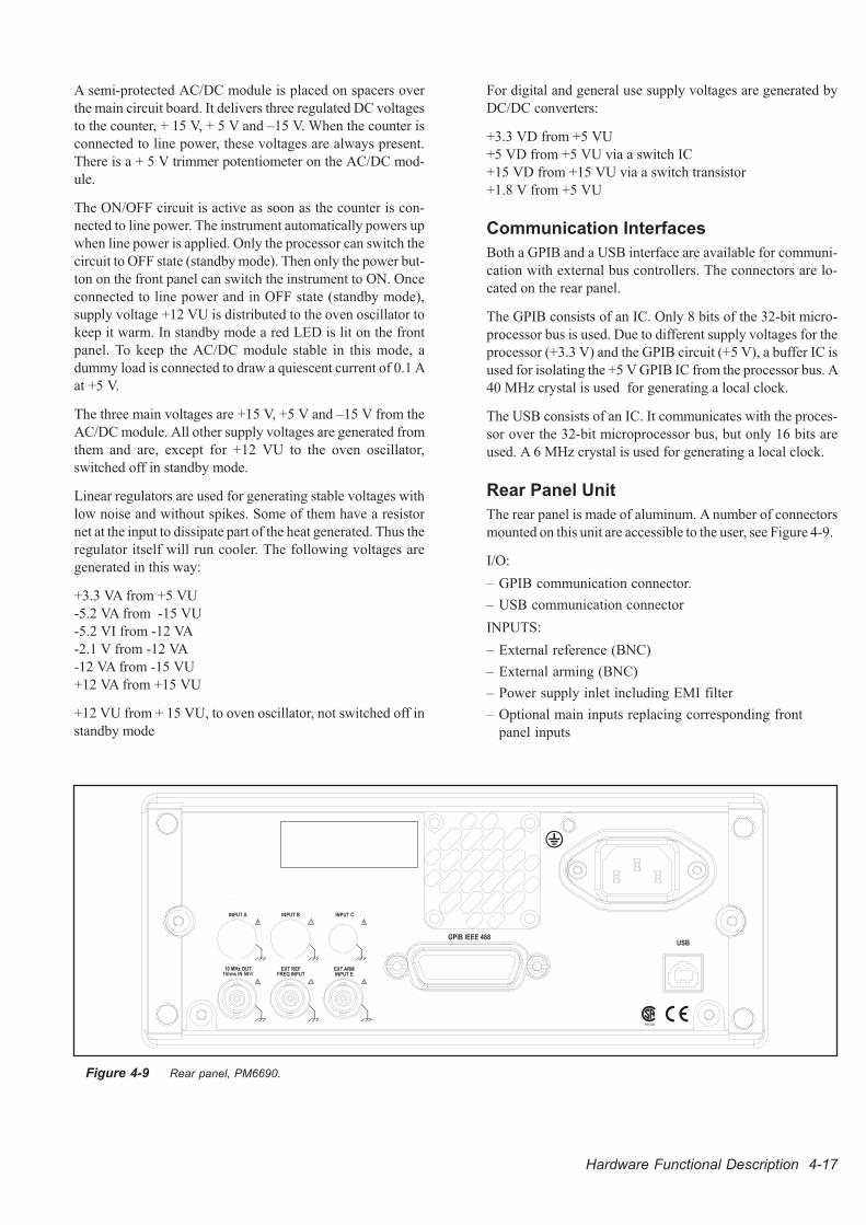
A semi-protected AC/DC module is placed on spacers over
the main circuit board. It delivers three regulated DC voltages
to the counter, + 15 V, + 5 V and –15 V. When the counter is
connected to line power, these voltages are always present.
There is a + 5 V trimmer potentiometer on the AC/DC mod-
ule.
The ON/OFF circuit is active as soon as the counter is con-
nected to line power. The instrument automatically powers up
when line power is applied. Only the processor can switch the
circuit to OFF state (standby mode). Then only the power but-
ton on the front panel can switch the instrument to ON. Once
connected to line power and in OFF state (standby mode),
supply voltage +12 VU is distributed to the oven oscillator to
keep it warm. In standby mode a red LED is lit on the front
panel. To keep the AC/DC module stable in this mode, a
dummy load is connected to draw a quiescent current of 0.1 A
at +5 V.
The three main voltages are +15 V, +5 V and –15 V from the
AC/DC module. All other supply voltages are generated from
them and are, except for +12 VU to the oven oscillator,
switched off in standby mode.
Linear regulators are used for generating stable voltages with
low noise and without spikes. Some of them have a resistor
net at the input to dissipate part of the heat generated. Thus the
regulator itself will run cooler. The following voltages are
generated in this way:
+3.3 VA from +5 VU
-5.2 VA from -15 VU
-5.2 VI from -12 VA
-2.1 V from -12 VA
-12 VA from -15 VU
+12 VA from +15 VU
+12 VU from + 15 VU, to oven oscillator, not switched off in
standby mode
For digital and general use supply voltages are generated by
DC/DC converters:
+3.3 VD from +5 VU
+5 VD from +5 VU via a switch IC
+15 VD from +15 VU via a switch transistor
+1.8 V from +5 VU
Communication Interfaces
Both a GPIB and a USB interface are available for communi-
cation with external bus controllers. The connectors are lo-
cated on the rear panel.
The GPIB consists of an IC. Only 8 bits of the 32-bit micro-
processor bus is used. Due to different supply voltages for the
processor (+3.3 V) and the GPIB circuit (+5 V), a buffer IC is
used for isolating the +5 V GPIB IC from the processor bus. A
40 MHz crystal is used for generating a local clock.
The USB consists of an IC. It communicates with the proces-
sor over the 32-bit microprocessor bus, but only 16 bits are
used. A 6 MHz crystal is used for generating a local clock.
Rear Panel Unit
The rear panel is made of aluminum. A number of connectors
mounted on this unit are accessible to the user, see Figure 4-9.
I/O:
– GPIB communication connector.
– USB communication connector
INPUTS:
– External reference (BNC)
– External arming (BNC)
– Power supply inlet including EMI filter
– Optional main inputs replacing corresponding front
panel inputs
Hardware Functional Description 4-17
!
!
!
!
!
!
10 MHz OUT1Vrms IN 50W
EXT REFFREQ INPUT
EXT ARMINPUT E
INPUT A INPUT B INPUT C
GPIB IEEE 488USB
191125
Figure 4-9 Rear panel, PM6690.
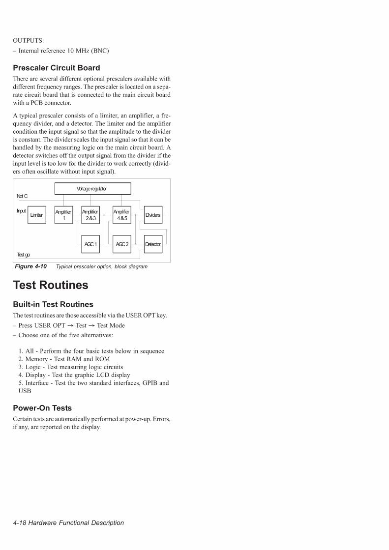
OUTPUTS:
– Internal reference 10 MHz (BNC)
Prescaler Circuit Board
There are several different optional prescalers available with
different frequency ranges. The prescaler is located on a sepa-
rate circuit board that is connected to the main circuit board
with a PCB connector.
A typical prescaler consists of a limiter, an amplifier, a fre-
quency divider, and a detector. The limiter and the amplifier
condition the input signal so that the amplitude to the divider
is constant. The divider scales the input signal so that it can be
handled by the measuring logic on the main circuit board. A
detector switches off the output signal from the divider if the
input level is too low for the divider to work correctly (divid-
ers often oscillate without input signal).
Test Routines
Built-in Test Routines
The test routines are those accessible via the USER OPT key.
– Press USER OPT � Test � Test Mode
– Choose one of the five alternatives:
1. All - Perform the four basic tests below in sequence
2. Memory - Test RAM and ROM
3. Logic - Test measuring logic circuits
4. Display - Test the graphic LCD display
5. Interface - Test the two standard interfaces, GPIB and
USB
Power-On Tests
Certain tests are automatically performed at power-up. Errors,
if any, are reported on the display.
4-18 Hardware Functional Description
LimiterAmplifier
1Amplifier
2&3Amplifier
4&5
AGC1 AGC2
Voltageregulator
Dividers
Detector
Not C
Test go
Input
Figure 4-10 Typical prescaler option, block diagram

Chapter 5
Corrective &
Preventive
Maintenance
Introduction
This chapter contains information about measures to be taken
for keeping the instrument in operative condition, or in other
words, what you can do to maintain the measurement accu-
racy, improve certain characteristics and prevent a break-
down.
Traditional troubleshooting is described in Chapter 6 - Repair.
Calibration
The single most important factor for maintaining the high per-
formance of your instrument is calibration on a regular basis.
A timer/counter is mainly used for time/frequency-related
measurements, so knowing the characteristics of your
timebase reference is vital to reliable results.
Scheduled calibration of the built-in timebase reference is
highly recommended in applications where external, more ac-
curate, frequency references are not available. Suitable cali-
bration intervals depend on the chosen timebase option and
the acceptable inaccuracy, but once a year is often a good
starting point.
The '90' has also limited voltage measurement capabilities,
and when these features are utilized, the voltage reference
should also be calibrated, preferably at the same time as the
frequency reference.
Both frequency and voltage calibration can be performed
without removing the cover, and the procedures are described
in Chapter 7, where you can also find information about cal-
culating calibration intervals for different timebase refer-
ences.
Instructions for FirmwareUpgrade
The firmware is stored in a FLASH PROM, so it is possible to
upgrade via one of the standard instrument interfaces (GPIB
or USB) without opening the case. USB is standard on most
PCs, but GPIB communication requires a special controller
board and dedicated SW from NI or CEC. A 'readme.txt' file
contains information not covered by these instructions. The
relevant files are available through the service organization.
– Make sure the National Instruments NI-VISA 3.2 or
later is installed with USB support, even though you are
going to use the GPIB interface for the upgrade.
– Establish a communication link between your PC and
the instrument over GPIB or USB by using a dedicated
application program, for instance NIMax from National
Instruments. No other instruments should be connected
to the same bus. Firmware upgrade over USB works
with firmware version V1.07 or above installed in the
instrument.
– Send *IDN? to the instrument and watch the response.
If the ID string is OK you can exit the communication
program and start the upgrading procedure.
– Download the latest firmware file (example name:
CNT_90_109_csl.hex) and the latest loader SW (exam-
ple name: Loader.exe) to a common directory on your
PC.
– Start the Loader.exe program.
– Press "Load" to open the firmware file. Follow the in-
structions on screen. The update is automatic, and pro-
cess information can be seen on the PC screen as well as
on the instrument display. Do not interrupt the process
too early as it may take between a few minutes up to an
hour, mostly depending on different possible hardware
combinations. A thermometer indicator on the PC moni-
tor gives status reports. The crucial part of the process is
when the message "FLASH updating (uninterruptible)"
is displayed. Do not under any circumstances interrupt
the loader while this message is visible. If the process
fails during this part, it may be impossible to control the
instrument from the bus as well as from the front panel.
Then you have to load new firmware over the JTAG
connection to the processor, a method that only the fac-
tory can apply.
– After a successful update, the counter is reset (if previ-
ous firmware is V1.01 and above). The message "Firm-
ware update complete. Loader is trying to connect to the
counter again" is displayed on the PC monitor. Confirm
by pressing OK.
– Press OK again when the message "Counter found" is
displayed.
– Press EXIT to leave the loader program.
– If the counter is not reset by the Loader program, turn
the counter off and on when the update is complete.
NOTE 1: With some firmware revisions and GPIB cards the
Loader gives an error message:
"Counter I/O error. Loader shutting down" after the
successful update. This is a loader fault and does not
harm the upgrade process.
– To remove the SRQ indicator on the front panel, which
might be present in such cases, start a GPIB communi-
cation tool and send the command "*PSC 1" and run a
full power cycle (OFF/ON).
NOTE 2: Some firmware revisions need a full power cycle to
resume proper operation. If the instrument does not
measure correctly after firmware upgrade, turn the in-
strument OFF and ON to initialize the hardware prop-
erly.
– After the update, enter the calibration menu (password
62951413) and run "Calibrate internals".
5-2 Introduction
Utility Program
Purpose
This service tool is used for configuring the timer/counter,
whenever information stored in firmware about serial number
and oscillator type etc. has been lost, for example after re-
placement of the main PCB. It is also used for defining a new
factory calibration.
Availability and System Requirements
The utility program can be obtained from the manufacturer or
your local service organization free of charge and can be run
on any PC with Windows 2K or XP equipped with a GPIB in-
terface from National Instruments. It is distributed as a com-
pressed file called PM6690.zip containing all the necessary
installation and data files including a readme.txt file with ad-
ditional information.
Installation
– Unpack the zip file in an empty directory by using
Winzip.
– Delete the original zip file if you want to save memory
space.
– Run the setup.exe program and follow the on-screen in-
structions.
Running the Application
After installation you can start the utility application by run-
ning the program PM6690 Utility.exe from the chosen direc-
tory. Refer to the readme.txt file for closer information on top-
ics not covered by the application user interface.
Fan Replacement
This instrument is equipped with a speed-controlled fan as
standard to sustain the specified operating temperature range.
If your instrument is operating in a 24 h/day system, you
should replace the fan every second year to maintain maxi-
mum reliability. For part-time applications and where low am-
bient temperatures prevail, an extended service interval is ac-
ceptable.
Follow the instructions on page 3-3 to replace the fan.
Other Important Information
There are no batteries of any kind in this instrument, so in gen-
eral it is only necessary to remove the cover when the fan is to
be replaced, or when a real fault calls for traditional trouble-
shooting.
Utility Program 5-3
This page is intentionally left blank.
5-4 Other Important Information

Chapter 6
Repair

This page is intentionally left blank.
6-2

Version A
The descriptions in this section apply to instru-
ments having a Triscend microprocessor.
See General Information on page III for details on
relevant serial numbers etc.
Version A 6-3

Troubleshooting
General
The '90' is a highly integrated Timer/Counter in which a dedi-
cated FPGA counter circuit handles the signal processing, and
a microcontroller does the postprocessing and supervising
jobs. A number of additional functional units support these
basic tasks, for instance power supply, reference oscillator,
wideband input amplifiers, comparators, memory (RAM &
ROM), digital/analog converters, etc.
The units are treated from a troubleshooting point of view in
this chapter, which means that units described earlier should
be considered faultless before troubleshooting on units de-
scribed later.
WARNING: Live parts and accessible termi-
nals which can be dangerous to life are
always exposed inside the unit when it is
connected to the line power. Use extreme
caution when handling, testing or adjust-
ing the counter.
Where to Start
After reading the safety instructions, continue with this
chapter for troubleshooting and repair instructions. When you
have fixed the instrument, always do the Safety Inspection
and Test after Repair, as described later in this Chapter. Then
do the checks in Chapter 2, Performance Check. Recalibrate if
required by following the adjustment instructions in Chapter
7, Calibration Adjustments.
Logic Levels
The '90' contains logic of different families. The levels of the
standard families are listed in Table 6-1. In addition to these
families there is also low-level logic requiring lower supply
voltages, e.g. +3.3 V, +2.5 V and +1.8 V.
Required Test Equipment
To be able to test the instrument properly using this manual
you will need the equipment listed in Table 2-1. The list con-
tains the critical parameter specifications.
Operating Conditions
Power voltage must be between 90 VAC and 260 VAC. The in-
strument adapts automatically to the applied voltage.
Basic Functional Units
These are the units that are described in this chapter with ref-
erence to the page where the section starts:
• Power Supply (p. 6-4)
• Input Amplifiers (p. 6-8)
• Timebase Reference Circuits (p. 6-12)
• Prescalers (p.6-15)
• Microprocessor & Memories (p. 6-15)
• Microprocessor Bus & Interfaces (p. 6-21)
• Measurement Logic (p. 6-27)
Power Supply
The DC voltages needed in the instrument are generated from
the three main voltages of the AC/DC module.
The instrument has only a secondary power switch, i.e. the
AC/DC module is always operating if line power is applied.
The three output DC voltages (+5 V, +15 V, -15 V) from the
module are present on the main circuit board. When switched
off, the instrument is in the standby mode. In this mode only
6-4 Troubleshooting
Positive
ECL
Negative
ECL
CMOS TTL
Supply voltage +5 V -5 V +5 V +5 V
Signal ground 0 V 0 V 0 V 0 V
Input voltage
High, VIH >+3.9 V >-1.1 V >+4 V >+2 V
Low, VIL <+3.5 V <-1.5 V <+1 V <+0.8 V
Output voltage
High, VOH >+4 V >-1 V >+4.9 V >+2.7 V
Low, VOL <+3.3 V <-1.7 V <+0.05 V <+0.4 V
Bias ref. voltage,
VBB+3.7 V -1.3 V - -
Table 6-1 Logic levels.
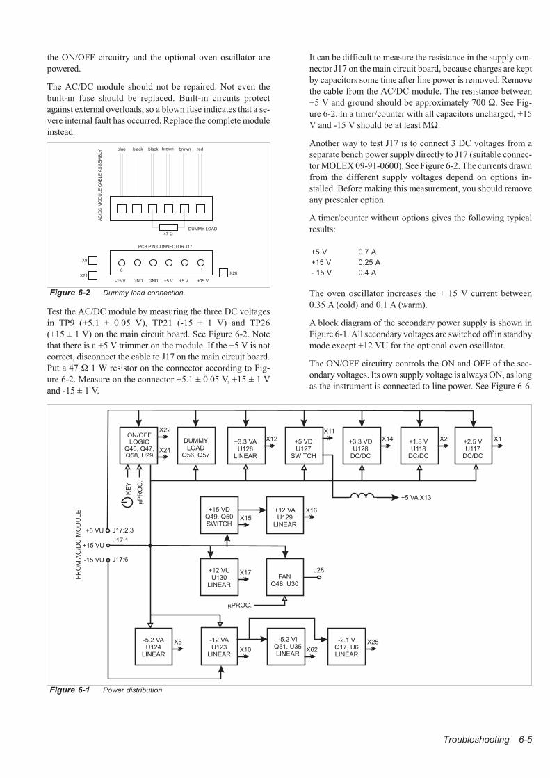
the ON/OFF circuitry and the optional oven oscillator are
powered.
The AC/DC module should not be repaired. Not even the
built-in fuse should be replaced. Built-in circuits protect
against external overloads, so a blown fuse indicates that a se-
vere internal fault has occurred. Replace the complete module
instead.
Test the AC/DC module by measuring the three DC voltages
in TP9 (+5.1 ± 0.05 V), TP21 (-15 ± 1 V) and TP26
(+15 ± 1 V) on the main circuit board. See Figure 6-2. Note
that there is a +5 V trimmer on the module. If the +5 V is not
correct, disconnect the cable to J17 on the main circuit board.
Put a 47 � 1 W resistor on the connector according to Fig-
ure 6-2. Measure on the connector +5.1 ± 0.05 V, +15 ± 1 V
and -15 ± 1 V.
It can be difficult to measure the resistance in the supply con-
nector J17 on the main circuit board, because charges are kept
by capacitors some time after line power is removed. Remove
the cable from the AC/DC module. The resistance between
+5 V and ground should be approximately 700 �. See Fig-
ure 6-2. In a timer/counter with all capacitors uncharged, +15
V and -15 V should be at least M�.
Another way to test J17 is to connect 3 DC voltages from a
separate bench power supply directly to J17 (suitable connec-
tor MOLEX 09-91-0600). See Figure 6-2. The currents drawn
from the different supply voltages depend on options in-
stalled. Before making this measurement, you should remove
any prescaler option.
A timer/counter without options gives the following typical
results:
+5 V 0.7 A
+15 V 0.25 A
- 15 V 0.4 A
The oven oscillator increases the + 15 V current between
0.35 A (cold) and 0.1 A (warm).
A block diagram of the secondary power supply is shown in
Figure 6-1. All secondary voltages are switched off in standby
mode except +12 VU for the optional oven oscillator.
The ON/OFF circuitry controls the ON and OFF of the sec-
ondary voltages. Its own supply voltage is always ON, as long
as the instrument is connected to line power. See Figure 6-6.
Troubleshooting 6-5
X1X2 +2.5 VU117
DC/DC
+1.8 VU118
DC/DC
+3.3 VDU128
DC/DC
+5 VDU127
SWITCH
X14
X11
+3.3 VAU126
LINEAR
X12DUMMYLOAD
Q56, Q57
ON/OFFLOGIC
Q46, Q47,Q58, U29
X22
X24
+12 VAU129
LINEAR
+15 VDQ49, Q50SWITCH
X15
+12 VUU130
LINEAR
X17FAN
Q48, U30
+15 VU
+5 VU
J28
X16
�PROC.
X10
-12 VAU123
LINEAR
-5.2 VAU124
LINEAR
X8
X62
X25
-15 VU
J17:2,3
J17:1
J17:6
FR
OM
AC
/DC
MO
DU
LE
+5 VA X13
�P
RO
C.
KE
Y
-5.2 VIQ51, U35LINEAR
-2.1 VQ17, U6LINEAR
Figure 6-1 Power distribution
47 �
redbrownbrownblackblackblue
AC
/DC
MO
DU
LE
CA
BL
EA
SS
EM
BLY
PCB PIN CONNECTOR J17
X26
X9
X21
+15 V+5 V+5 VGNDGND-15 V
DUMMY LOAD
16
Figure 6-2 Dummy load connection.
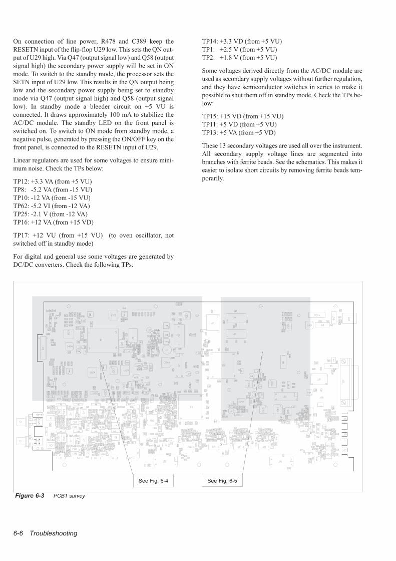
On connection of line power, R478 and C389 keep the
RESETN input of the flip-flop U29 low. This sets the QN out-
put of U29 high. Via Q47 (output signal low) and Q58 (output
signal high) the secondary power supply will be set in ON
mode. To switch to the standby mode, the processor sets the
SETN input of U29 low. This results in the QN output being
low and the secondary power supply being set to standby
mode via Q47 (output signal high) and Q58 (output signal
low). In standby mode a bleeder circuit on +5 VU is
connected. It draws approximately 100 mA to stabilize the
AC/DC module. The standby LED on the front panel is
switched on. To switch to ON mode from standby mode, a
negative pulse, generated by pressing the ON/OFF key on the
front panel, is connected to the RESETN input of U29.
Linear regulators are used for some voltages to ensure mini-
mum noise. Check the TPs below:
TP12: +3.3 VA (from +5 VU)
TP8: -5.2 VA (from -15 VU)
TP10: -12 VA (from -15 VU)
TP62: -5.2 VI (from -12 VA)
TP25: -2.1 V (from -12 VA)
TP16: +12 VA (from +15 VD)
TP17: +12 VU (from +15 VU) (to oven oscillator, not
switched off in standby mode)
For digital and general use some voltages are generated by
DC/DC converters. Check the following TPs:
TP14: +3.3 VD (from +5 VU)
TP1: +2.5 V (from +5 VU)
TP2: +1.8 V (from +5 VU)
Some voltages derived directly from the AC/DC module are
used as secondary supply voltages without further regulation,
and they have semiconductor switches in series to make it
possible to shut them off in standby mode. Check the TPs be-
low:
TP15: +15 VD (from +15 VU)
TP11: +5 VD (from +5 VU)
TP13: +5 VA (from +5 VD)
These 13 secondary voltages are used all over the instrument.
All secondary supply voltage lines are segmented into
branches with ferrite beads. See the schematics. This makes it
easier to isolate short circuits by removing ferrite beads tem-
porarily.
6-6 Troubleshooting
Figure 6-3 PCB1 survey
See Fig. 6-4 See Fig. 6-5
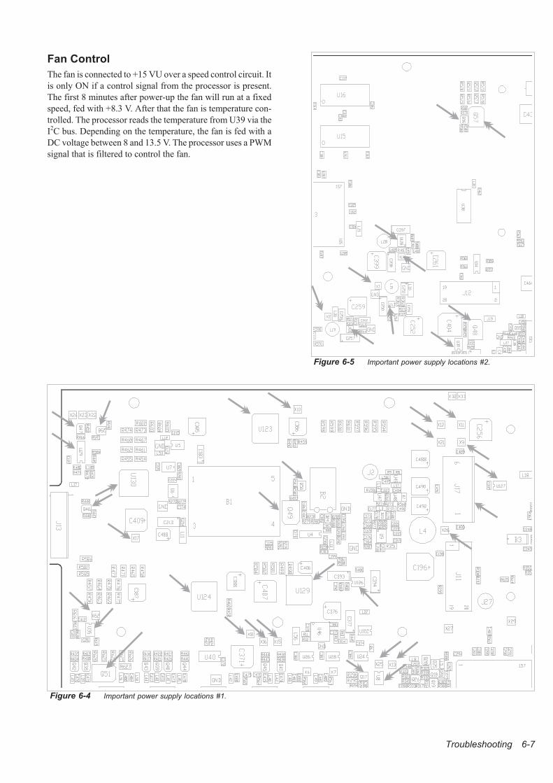
Fan Control
The fan is connected to +15 VU over a speed control circuit. It
is only ON if a control signal from the processor is present.
The first 8 minutes after power-up the fan will run at a fixed
speed, fed with +8.3 V. After that the fan is temperature con-
trolled. The processor reads the temperature from U39 via the
I2C bus. Depending on the temperature, the fan is fed with a
DC voltage between 8 and 13.5 V. The processor uses a PWM
signal that is filtered to control the fan.
Troubleshooting 6-7
Figure 6-4 Important power supply locations #1.
Figure 6-5 Important power supply locations #2.
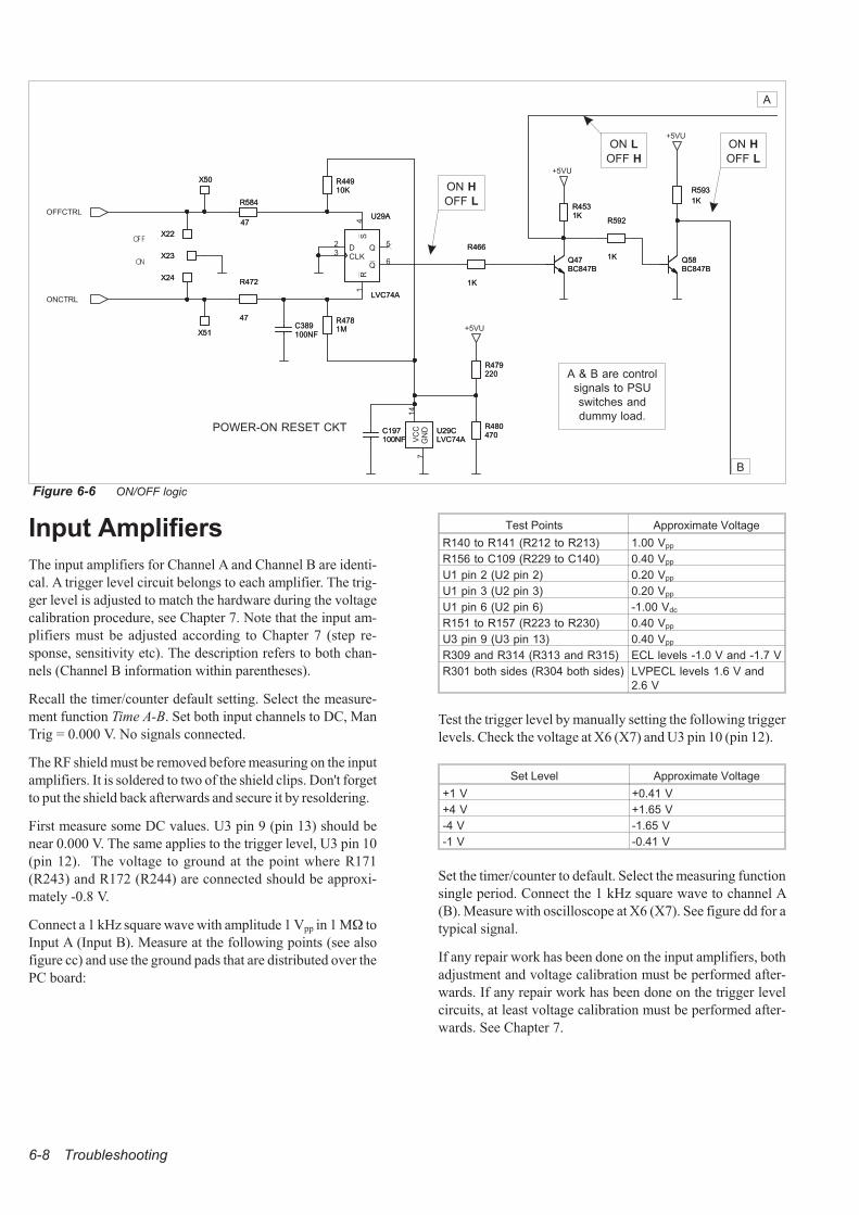
Input Amplifiers
The input amplifiers for Channel A and Channel B are identi-
cal. A trigger level circuit belongs to each amplifier. The trig-
ger level is adjusted to match the hardware during the voltage
calibration procedure, see Chapter 7. Note that the input am-
plifiers must be adjusted according to Chapter 7 (step re-
sponse, sensitivity etc). The description refers to both chan-
nels (Channel B information within parentheses).
Recall the timer/counter default setting. Select the measure-
ment function Time A-B. Set both input channels to DC, Man
Trig = 0.000 V. No signals connected.
The RF shield must be removed before measuring on the input
amplifiers. It is soldered to two of the shield clips. Don't forget
to put the shield back afterwards and secure it by resoldering.
First measure some DC values. U3 pin 9 (pin 13) should be
near 0.000 V. The same applies to the trigger level, U3 pin 10
(pin 12). The voltage to ground at the point where R171
(R243) and R172 (R244) are connected should be approxi-
mately -0.8 V.
Connect a 1 kHz square wave with amplitude 1 Vpp in 1 M� to
Input A (Input B). Measure at the following points (see also
figure cc) and use the ground pads that are distributed over the
PC board:
Test Points Approximate Voltage
R140 to R141 (R212 to R213) 1.00 Vpp
R156 to C109 (R229 to C140) 0.40 Vpp
U1 pin 2 (U2 pin 2) 0.20 Vpp
U1 pin 3 (U2 pin 3) 0.20 Vpp
U1 pin 6 (U2 pin 6) -1.00 Vdc
R151 to R157 (R223 to R230) 0.40 Vpp
U3 pin 9 (U3 pin 13) 0.40 Vpp
R309 and R314 (R313 and R315) ECL levels -1.0 V and -1.7 V
R301 both sides (R304 both sides) LVPECL levels 1.6 V and
2.6 V
Test the trigger level by manually setting the following trigger
levels. Check the voltage at X6 (X7) and U3 pin 10 (pin 12).
Set Level Approximate Voltage
+1 V +0.41 V
+4 V +1.65 V
-4 V -1.65 V
-1 V -0.41 V
Set the timer/counter to default. Select the measuring function
single period. Connect the 1 kHz square wave to channel A
(B). Measure with oscilloscope at X6 (X7). See figure dd for a
typical signal.
If any repair work has been done on the input amplifiers, both
adjustment and voltage calibration must be performed after-
wards. If any repair work has been done on the trigger level
circuits, at least voltage calibration must be performed after-
wards. See Chapter 7.
6-8 Troubleshooting
+5VU
+5VU
+5VU
OFFCTRL
ONCTRL
ON
OFF
C389100NFC389100NF
R593
1K
R593
1K
R592
1K
R592
1K
R44910KR44910K
X51X51
Q58BC847BQ58BC847B
X22X22
X50X50
VC
C1
4
GN
D7
U29CLVC74AU29CLVC74A
R479220R479220
C197100NFC197100NF
R466
1K
R466
1KX24X24
Q47BC847BQ47BC847B
R472
47
R472
47
X23X23
R4531KR4531K
1MR4781MR478
R584
47
R584
47
D2
CLK3
S4
R1
Q5
Q6
U29A
LVC74A
U29A
LVC74A
R480470R480470
Figure 6-6 ON/OFF logic
ON H
OFF L
ON H
OFF L
ON L
OFF H
A & B are control
signals to PSU
switches and
dummy load.POWER-ON RESET CKT
A
B
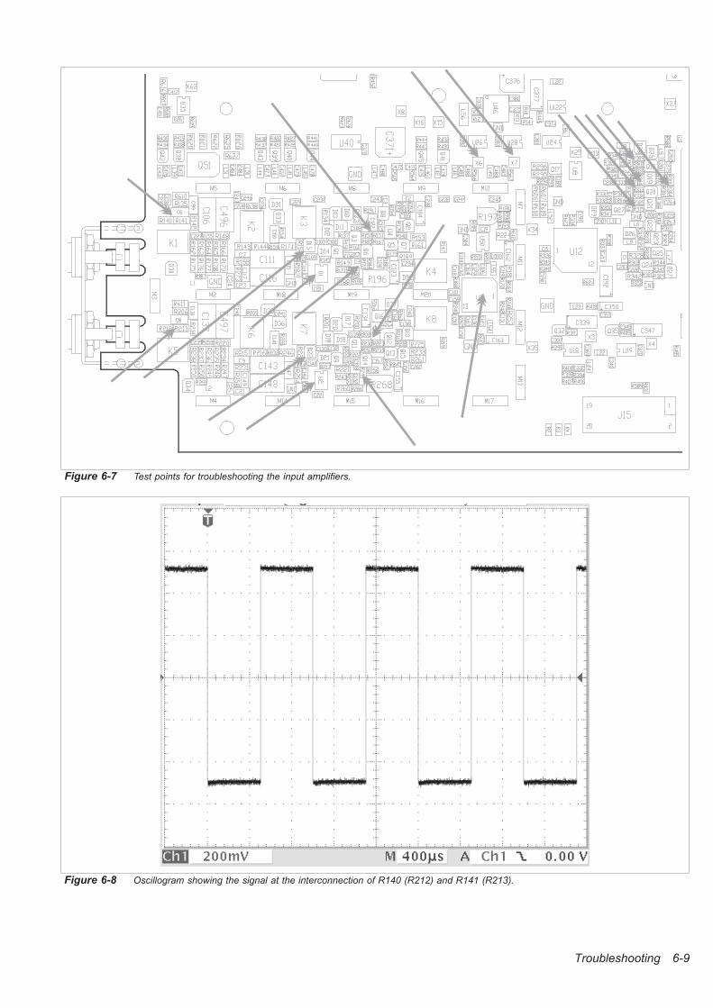
Troubleshooting 6-9
Figure 6-7 Test points for troubleshooting the input amplifiers.
Figure 6-8 Oscillogram showing the signal at the interconnection of R140 (R212) and R141 (R213).
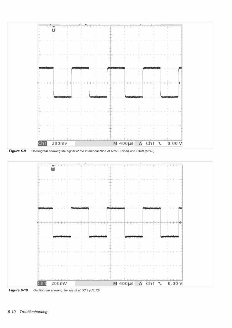
6-10 Troubleshooting
Figure 6-9 Oscillogram showing the signal at the interconnection of R156 (R229) and C109 (C140).
Figure 6-10 Oscillogram showing the signal at U3:9 (U3:13).

Troubleshooting 6-11
Figure 6-11 Oscillogram showing the signal at U1:2 (U2:2).
Figure 6-12 Oscillogram showing the signal at X6, Period Single A.
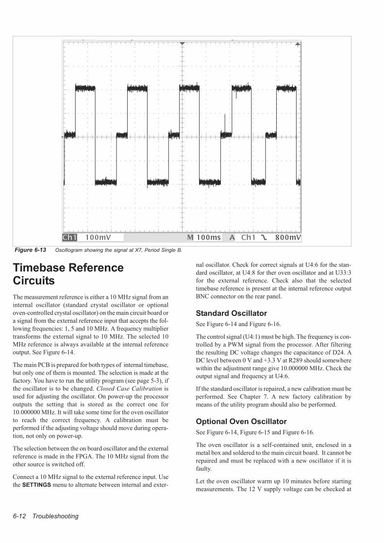
Timebase ReferenceCircuits
The measurement reference is either a 10 MHz signal from an
internal oscillator (standard crystal oscillator or optional
oven-controlled crystal oscillator) on the main circuit board or
a signal from the external reference input that accepts the fol-
lowing frequencies: 1, 5 and 10 MHz. A frequency multiplier
transforms the external signal to 10 MHz. The selected 10
MHz reference is always available at the internal reference
output. See Figure 6-14.
The main PCB is prepared for both types of internal timebase,
but only one of them is mounted. The selection is made at the
factory. You have to run the utility program (see page 5-3), if
the oscillator is to be changed. Closed Case Calibration is
used for adjusting the oscillator. On power-up the processor
outputs the setting that is stored as the correct one for
10.000000 MHz. It will take some time for the oven oscillator
to reach the correct frequency. A calibration must be
performed if the adjusting voltage should move during opera-
tion, not only on power-up.
The selection between the on board oscillator and the external
reference is made in the FPGA. The 10 MHz signal from the
other source is switched off.
Connect a 10 MHz signal to the external reference input. Use
the SETTINGS menu to alternate between internal and exter-
nal oscillator. Check for correct signals at U4:6 for the stan-
dard oscillator, at U4:8 for ther oven oscillator and at U33:3
for the external reference. Check also that the selected
timebase reference is present at the internal reference output
BNC connector on the rear panel.
Standard Oscillator
See Figure 6-14 and Figure 6-16.
The control signal (U4:1) must be high. The frequency is con-
trolled by a PWM signal from the processor. After filtering
the resulting DC voltage changes the capacitance of D24. A
DC level between 0 V and +3.3 V at R289 should somewhere
within the adjustment range give 10.000000 MHz. Check the
output signal and frequency at U4:6.
If the standard oscillator is repaired, a new calibration must be
performed. See Chapter 7. A new factory calibration by
means of the utility program should also be performed.
Optional Oven Oscillator
See Figure 6-14, Figure 6-15 and Figure 6-16.
The oven oscillator is a self-contained unit, enclosed in a
metal box and soldered to the main circuit board. It cannot be
repaired and must be replaced with a new oscillator if it is
faulty.
Let the oven oscillator warm up 10 minutes before starting
measurements. The 12 V supply voltage can be checked at
6-12 Troubleshooting
Figure 6-13 Oscillogram showing the signal at X7, Period Single B.
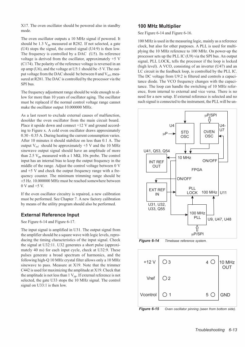
X17. The oven oscillator should be powered also in standby
mode.
The oven oscillator outputs a 10 MHz signal if powered. It
should be 1.3 Vpp measured at R282. If not selected, a gate
(U4) stops the signal, the control signal (U4:9) is then low.
The frequency is controlled by a DAC (U5). Its reference
voltage is derived from the oscillator, approximately +5 V
(C174). The polarity of the reference voltage is reversed in an
op amp (U6), and the voltage at U5:1 should be -5 V. The out-
put voltage from the DAC should be between 0 and Vref, mea-
sured at R281. The DAC is controlled by the processor via the
SPI bus.
The frequency adjustment range should be wide enough to al-
low for more than 10 years of oscillator aging. The oscillator
must be replaced if the normal control voltage range cannot
make the oscillator output 10.000000 MHz.
As a last resort to exclude external causes of malfunction,
desolder the oven oscillator from the main circuit board.
Place it upside down and connect +12 V and ground accord-
ing to Figure x. A cold oven oscillator draws approximately
0.30 - 0.35 A. During heating the current consumption varies.
After 10 minutes it should stabilize on less than 0.1 A. The
output Vref should be approximately +5 V and the 10 MHz
sinewave output signal should have an amplitude of more
than 2.5 Vpp measured with a 1 M�, 10x probe. The control
input has an internal bias to keep the output frequency in the
middle of the range. Adjust the control voltage between 0 V
and +5 V and check the output frequency range with a fre-
quency counter. The minimum trimming range should be
±5 Hz. 10.000000 MHz must be reached somewhere between
0 V and +5 V.
If the oven oscillator circuitry is repaired, a new calibration
must be performed. See Chapter 7. A new factory calibration
by means of the utility program should also be performed.
External Reference Input
See Figure 6-14 and Figure 6-17.
The input signal is amplified in U31. The output signal from
the amplifier should be a square wave with logic levels, repro-
ducing the timing characteristics of the input signal. Check
the signal at U32:11. U32 generates a short pulse (approxi-
mately 40 ns) for each input cycle, check at U32:9. These
pulses generate a broad spectrum of harmonics, and the
following high-Q 10 MHz crystal filter allows only a 10 MHz
sinewave to pass. Measure at X19. Note that the trimmer
C442 is used for maximizing the amplitude at X19. Check that
the amplitude is not less than 1 Vpp. If external reference is not
selected, the gate U33 stops the 10 MHz signal. The control
signal on U33:1 is then low.
100 MHz Multiplier
See Figure 6-14 and Figure 6-16.
100 MHz is used in the measuring logic, mainly as a reference
clock, but also for other purposes. A PLL is used for multi-
plying the 10 MHz reference to 100 MHz. On power-up the
processor sets up the PLL IC (U9) via the SPI bus. An output
signal, PLL LOCK, tells the processor if the loop is locked
(high level). A VCO, consisting of an inverter (U47) and an
LC circuit in the feedback loop, is controlled by the PLL IC.
The DC voltage from U9:2 is filtered and controls a capaci-
tance diode. The VCO frequency changes with the capaci-
tance. The loop can handle the switching of 10 MHz refer-
ence, from internal to external and vice versa. There is no
need for a new setup. If external reference is selected and no
such signal is connected to the instrument, the PLL will be un-
Troubleshooting 6-13
FPGA
100 MHzPLL
EXT REFIN
INT REFOUT
STDOSC
OVENOSC
U4 U4-U7
10 MHz
U11
ON/OFF
100 MHzPLL
LOCK
ON/OFF
�P/SPI
�P
�P/SPI
U41, Q53, Q54
U31, U32,U33, Q55
U9, U47, U48
Figure 6-14 Timebase reference system.
3
2
1 5
4+12 V
Vref
Vcontrol GND
10 MHzOUT
Figure 6-15 Oven oscillator pinning (seen from bottom side).
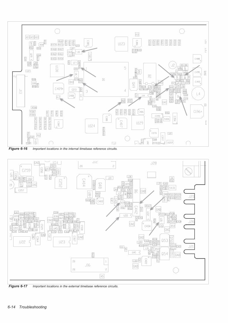
6-14 Troubleshooting
Figure 6-16 Important locations in the internal timebase reference circuits.
Figure 6-17 Important locations in the external timebase reference circuits.
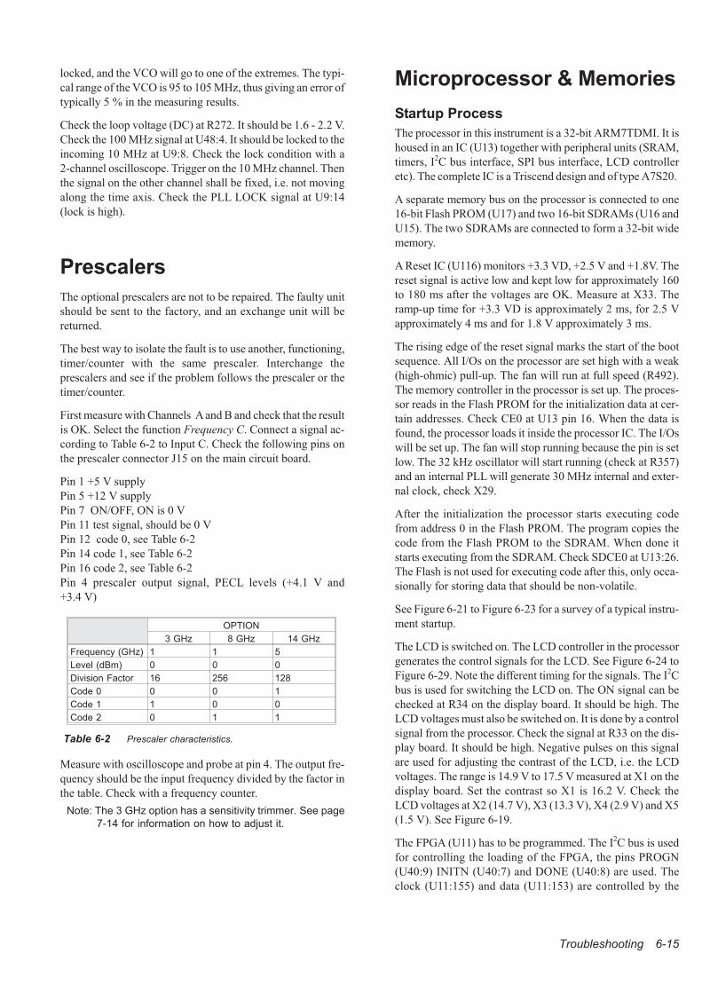
locked, and the VCO will go to one of the extremes. The typi-
cal range of the VCO is 95 to 105 MHz, thus giving an error of
typically 5 % in the measuring results.
Check the loop voltage (DC) at R272. It should be 1.6 - 2.2 V.
Check the 100 MHz signal at U48:4. It should be locked to the
incoming 10 MHz at U9:8. Check the lock condition with a
2-channel oscilloscope. Trigger on the 10 MHz channel. Then
the signal on the other channel shall be fixed, i.e. not moving
along the time axis. Check the PLL LOCK signal at U9:14
(lock is high).
Prescalers
The optional prescalers are not to be repaired. The faulty unit
should be sent to the factory, and an exchange unit will be
returned.
The best way to isolate the fault is to use another, functioning,
timer/counter with the same prescaler. Interchange the
prescalers and see if the problem follows the prescaler or the
timer/counter.
First measure with Channels A and B and check that the result
is OK. Select the function Frequency C. Connect a signal ac-
cording to Table 6-2 to Input C. Check the following pins on
the prescaler connector J15 on the main circuit board.
Pin 1 +5 V supply
Pin 5 +12 V supply
Pin 7 ON/OFF, ON is 0 V
Pin 11 test signal, should be 0 V
Pin 12 code 0, see Table 6-2
Pin 14 code 1, see Table 6-2
Pin 16 code 2, see Table 6-2
Pin 4 prescaler output signal, PECL levels (+4.1 V and
+3.4 V)
Measure with oscilloscope and probe at pin 4. The output fre-
quency should be the input frequency divided by the factor in
the table. Check with a frequency counter.
Note: The 3 GHz option has a sensitivity trimmer. See page
7-14 for information on how to adjust it.
Microprocessor & Memories
Startup Process
The processor in this instrument is a 32-bit ARM7TDMI. It is
housed in an IC (U13) together with peripheral units (SRAM,
timers, I2C bus interface, SPI bus interface, LCD controller
etc). The complete IC is a Triscend design and of type A7S20.
A separate memory bus on the processor is connected to one
16-bit Flash PROM (U17) and two 16-bit SDRAMs (U16 and
U15). The two SDRAMs are connected to form a 32-bit wide
memory.
A Reset IC (U116) monitors +3.3 VD, +2.5 V and +1.8V. The
reset signal is active low and kept low for approximately 160
to 180 ms after the voltages are OK. Measure at X33. The
ramp-up time for +3.3 VD is approximately 2 ms, for 2.5 V
approximately 4 ms and for 1.8 V approximately 3 ms.
The rising edge of the reset signal marks the start of the boot
sequence. All I/Os on the processor are set high with a weak
(high-ohmic) pull-up. The fan will run at full speed (R492).
The memory controller in the processor is set up. The proces-
sor reads in the Flash PROM for the initialization data at cer-
tain addresses. Check CE0 at U13 pin 16. When the data is
found, the processor loads it inside the processor IC. The I/Os
will be set up. The fan will stop running because the pin is set
low. The 32 kHz oscillator will start running (check at R357)
and an internal PLL will generate 30 MHz internal and exter-
nal clock, check X29.
After the initialization the processor starts executing code
from address 0 in the Flash PROM. The program copies the
code from the Flash PROM to the SDRAM. When done it
starts executing from the SDRAM. Check SDCE0 at U13:26.
The Flash is not used for executing code after this, only occa-
sionally for storing data that should be non-volatile.
See Figure 6-21 to Figure 6-23 for a survey of a typical instru-
ment startup.
The LCD is switched on. The LCD controller in the processor
generates the control signals for the LCD. See Figure 6-24 to
Figure 6-29. Note the different timing for the signals. The I2C
bus is used for switching the LCD on. The ON signal can be
checked at R34 on the display board. It should be high. The
LCD voltages must also be switched on. It is done by a control
signal from the processor. Check the signal at R33 on the dis-
play board. It should be high. Negative pulses on this signal
are used for adjusting the contrast of the LCD, i.e. the LCD
voltages. The range is 14.9 V to 17.5 V measured at X1 on the
display board. Set the contrast so X1 is 16.2 V. Check the
LCD voltages at X2 (14.7 V), X3 (13.3 V), X4 (2.9 V) and X5
(1.5 V). See Figure 6-19.
The FPGA (U11) has to be programmed. The I2C bus is used
for controlling the loading of the FPGA, the pins PROGN
(U40:9) INITN (U40:7) and DONE (U40:8) are used. The
clock (U11:155) and data (U11:153) are controlled by the
Troubleshooting 6-15
OPTION
3 GHz 8 GHz 14 GHz
Frequency (GHz) 1 1 5
Level (dBm) 0 0 0
Division Factor 16 256 128
Code 0 0 0 1
Code 1 1 0 0
Code 2 0 1 1
Table 6-2 Prescaler characteristics.
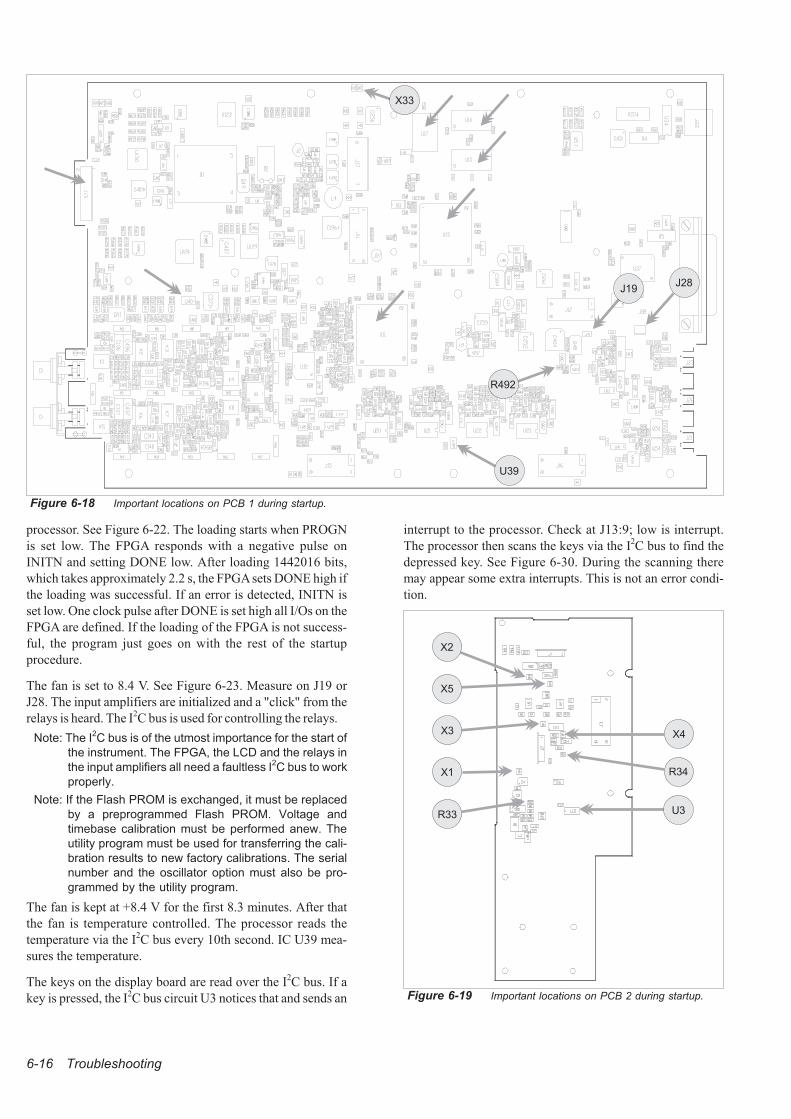
processor. See Figure 6-22. The loading starts when PROGN
is set low. The FPGA responds with a negative pulse on
INITN and setting DONE low. After loading 1442016 bits,
which takes approximately 2.2 s, the FPGAsets DONE high if
the loading was successful. If an error is detected, INITN is
set low. One clock pulse after DONE is set high all I/Os on the
FPGA are defined. If the loading of the FPGA is not success-
ful, the program just goes on with the rest of the startup
procedure.
The fan is set to 8.4 V. See Figure 6-23. Measure on J19 or
J28. The input amplifiers are initialized and a "click" from the
relays is heard. The I2C bus is used for controlling the relays.
Note: The I2C bus is of the utmost importance for the start of
the instrument. The FPGA, the LCD and the relays in
the input amplifiers all need a faultless I2C bus to work
properly.
Note: If the Flash PROM is exchanged, it must be replaced
by a preprogrammed Flash PROM. Voltage and
timebase calibration must be performed anew. The
utility program must be used for transferring the cali-
bration results to new factory calibrations. The serial
number and the oscillator option must also be pro-
grammed by the utility program.
The fan is kept at +8.4 V for the first 8.3 minutes. After that
the fan is temperature controlled. The processor reads the
temperature via the I2C bus every 10th second. IC U39 mea-
sures the temperature.
The keys on the display board are read over the I2C bus. If a
key is pressed, the I2C bus circuit U3 notices that and sends an
interrupt to the processor. Check at J13:9; low is interrupt.
The processor then scans the keys via the I2C bus to find the
depressed key. See Figure 6-30. During the scanning there
may appear some extra interrupts. This is not an error condi-
tion.
6-16 Troubleshooting
Figure 6-18 Important locations on PCB 1 during startup.
J19
R492
J28
U39
X33
Figure 6-19 Important locations on PCB 2 during startup.
X3
X2
X5
X1
R33 U3
R34
X4
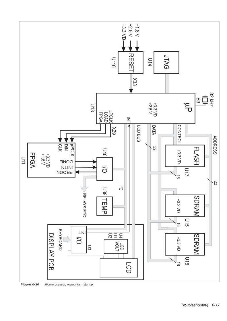
Troubleshooting 6-17
JTAG
RE
SE
T+
1.8
V
+2.5
V
+3.3
VD
X3
3
32
kHz�P
B3
FL
AS
HS
DR
AM
SD
RA
M
AD
DR
ES
S
CO
NT
RO
L
U1
4
U11
6
U1
3
DIS
PL
AY
PC
B
FP
GA
DA
TA
LC
DB
US
LC
DV
OLT
U1
7U
15
U1
6
U4
U1
U2
LC
D
I/O
U3
KE
YB
OA
RD
U11
TE
MP
U3
9
IC 2
I/OU
40
INT
INT
RE
LA
YS
ET
C.
INITN
DONE
PROGN
�P
CL
K
�P
CL
KLO
AD
FP
GA
CL
K
X2
9
+3.3
VD
+2.5
V
+3.3
VD
+1.8
V
+3.3
VD
+3.3
VD
+3.3
VD
22
16
16
16
32
DIN
Figure 6-20 Microprocessor, memories - startup.
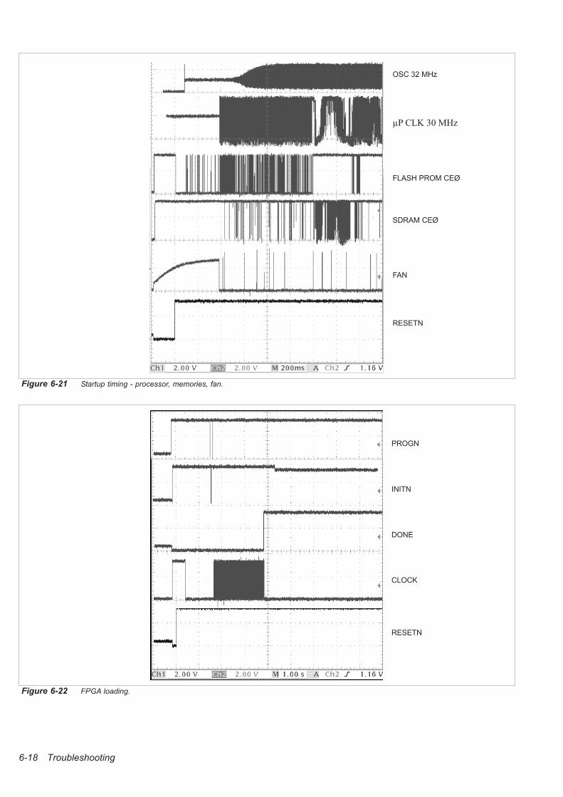
6-18 Troubleshooting
Figure 6-21 Startup timing - processor, memories, fan.
RESETN
FAN
SDRAM CEØ
FLASH PROM CEØ
µP CLK 30 MHz
OSC 32 MHz
Figure 6-22 FPGA loading.
PROGN
INITN
DONE
CLOCK
RESETN
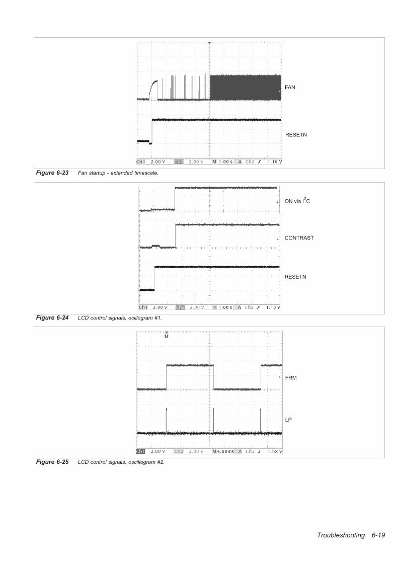
Troubleshooting 6-19
Figure 6-23 Fan startup - extended timescale.
FAN
RESETN
Figure 6-24 LCD control signals, ocillogram #1.
ON via I2C
CONTRAST
RESETN
Figure 6-25 LCD control signals, oscillogram #2.
FRM
LP
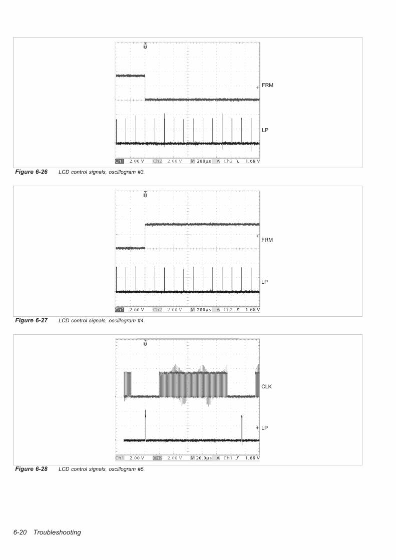
6-20 Troubleshooting
Figure 6-26 LCD control signals, oscillogram #3.
FRM
LP
Figure 6-27 LCD control signals, oscillogram #4.
LP
FRM
Figure 6-28 LCD control signals, oscillogram #5.
LP
CLK
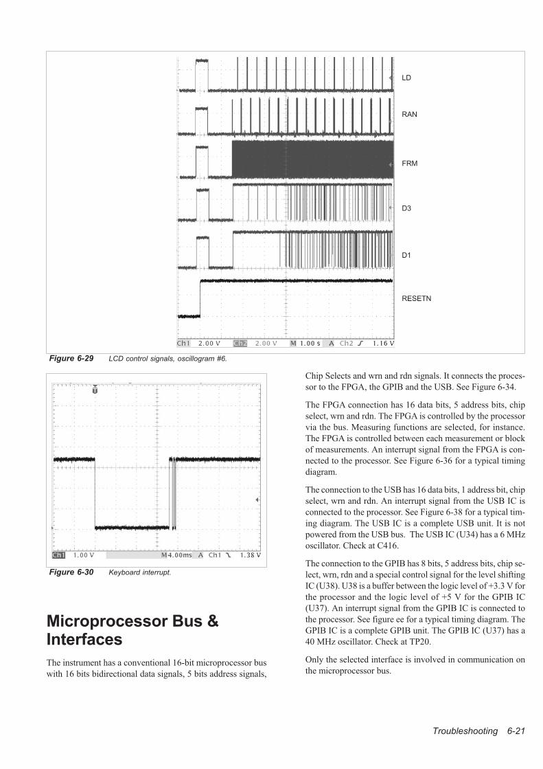
Microprocessor Bus &Interfaces
The instrument has a conventional 16-bit microprocessor bus
with 16 bits bidirectional data signals, 5 bits address signals,
Chip Selects and wrn and rdn signals. It connects the proces-
sor to the FPGA, the GPIB and the USB. See Figure 6-34.
The FPGA connection has 16 data bits, 5 address bits, chip
select, wrn and rdn. The FPGA is controlled by the processor
via the bus. Measuring functions are selected, for instance.
The FPGA is controlled between each measurement or block
of measurements. An interrupt signal from the FPGA is con-
nected to the processor. See Figure 6-36 for a typical timing
diagram.
The connection to the USB has 16 data bits, 1 address bit, chip
select, wrn and rdn. An interrupt signal from the USB IC is
connected to the processor. See Figure 6-38 for a typical tim-
ing diagram. The USB IC is a complete USB unit. It is not
powered from the USB bus. The USB IC (U34) has a 6 MHz
oscillator. Check at C416.
The connection to the GPIB has 8 bits, 5 address bits, chip se-
lect, wrn, rdn and a special control signal for the level shifting
IC (U38). U38 is a buffer between the logic level of +3.3 V for
the processor and the logic level of +5 V for the GPIB IC
(U37). An interrupt signal from the GPIB IC is connected to
the processor. See figure ee for a typical timing diagram. The
GPIB IC is a complete GPIB unit. The GPIB IC (U37) has a
40 MHz oscillator. Check at TP20.
Only the selected interface is involved in communication on
the microprocessor bus.
Troubleshooting 6-21
Figure 6-29 LCD control signals, oscillogram #6.
Figure 6-30 Keyboard interrupt.
LD
RESETN
RAN
FRM
D3
D1
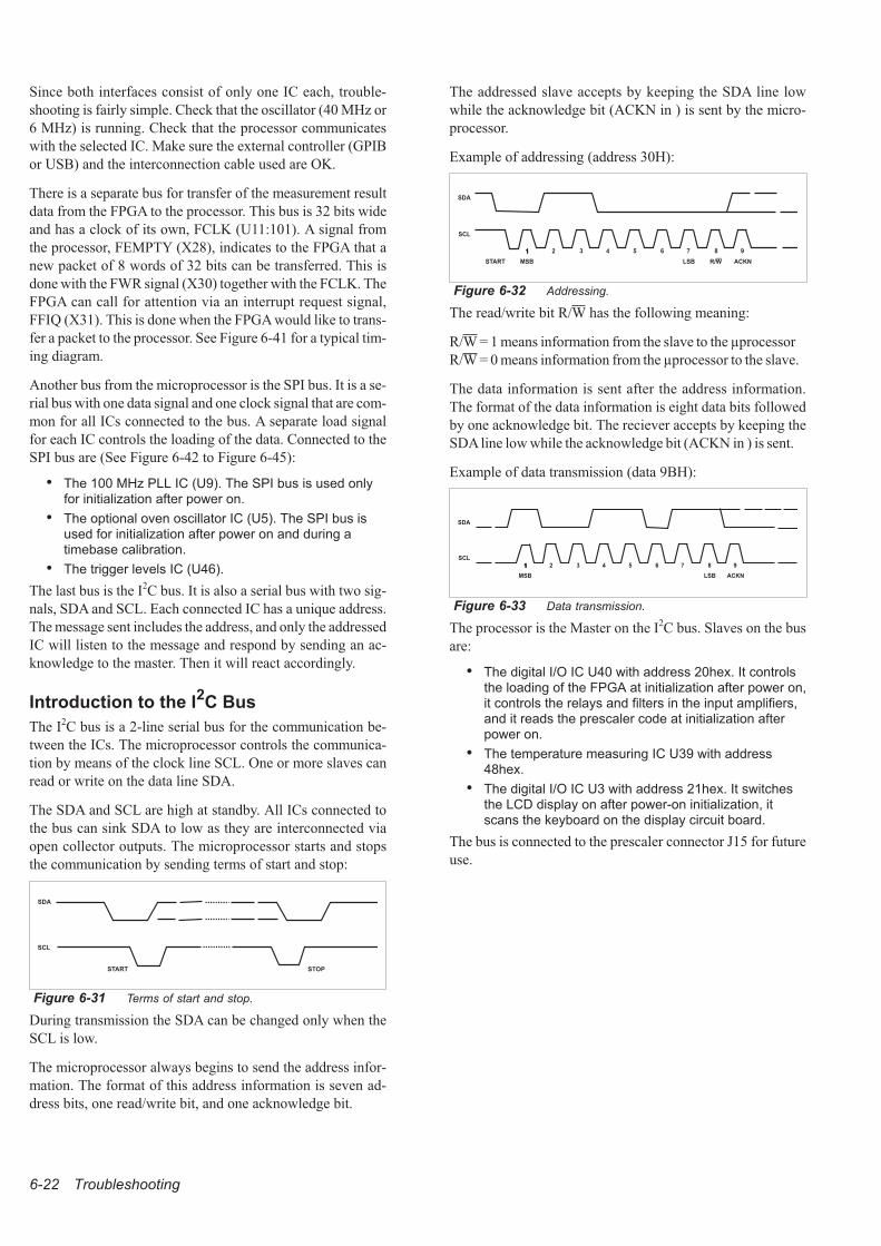
Since both interfaces consist of only one IC each, trouble-
shooting is fairly simple. Check that the oscillator (40 MHz or
6 MHz) is running. Check that the processor communicates
with the selected IC. Make sure the external controller (GPIB
or USB) and the interconnection cable used are OK.
There is a separate bus for transfer of the measurement result
data from the FPGA to the processor. This bus is 32 bits wide
and has a clock of its own, FCLK (U11:101). A signal from
the processor, FEMPTY (X28), indicates to the FPGA that a
new packet of 8 words of 32 bits can be transferred. This is
done with the FWR signal (X30) together with the FCLK. The
FPGA can call for attention via an interrupt request signal,
FFIQ (X31). This is done when the FPGA would like to trans-
fer a packet to the processor. See Figure 6-41 for a typical tim-
ing diagram.
Another bus from the microprocessor is the SPI bus. It is a se-
rial bus with one data signal and one clock signal that are com-
mon for all ICs connected to the bus. A separate load signal
for each IC controls the loading of the data. Connected to the
SPI bus are (See Figure 6-42 to Figure 6-45):
• The 100 MHz PLL IC (U9). The SPI bus is used onlyfor initialization after power on.
• The optional oven oscillator IC (U5). The SPI bus isused for initialization after power on and during atimebase calibration.
• The trigger levels IC (U46).
The last bus is the I2C bus. It is also a serial bus with two sig-
nals, SDA and SCL. Each connected IC has a unique address.
The message sent includes the address, and only the addressed
IC will listen to the message and respond by sending an ac-
knowledge to the master. Then it will react accordingly.
Introduction to the I2C Bus
The I2C bus is a 2-line serial bus for the communication be-
tween the ICs. The microprocessor controls the communica-
tion by means of the clock line SCL. One or more slaves can
read or write on the data line SDA.
The SDA and SCL are high at standby. All ICs connected to
the bus can sink SDA to low as they are interconnected via
open collector outputs. The microprocessor starts and stops
the communication by sending terms of start and stop:
During transmission the SDA can be changed only when the
SCL is low.
The microprocessor always begins to send the address infor-
mation. The format of this address information is seven ad-
dress bits, one read/write bit, and one acknowledge bit.
The addressed slave accepts by keeping the SDA line low
while the acknowledge bit (ACKN in ) is sent by the micro-
processor.
Example of addressing (address 30H):
The read/write bit R/W has the following meaning:
R/W = 1 means information from the slave to the µprocessor
R/W = 0 means information from the µprocessor to the slave.
The data information is sent after the address information.
The format of the data information is eight data bits followed
by one acknowledge bit. The reciever accepts by keeping the
SDAline low while the acknowledge bit (ACKN in ) is sent.
Example of data transmission (data 9BH):
The processor is the Master on the I2C bus. Slaves on the bus
are:
• The digital I/O IC U40 with address 20hex. It controlsthe loading of the FPGA at initialization after power on,it controls the relays and filters in the input amplifiers,and it reads the prescaler code at initialization afterpower on.
• The temperature measuring IC U39 with address48hex.
• The digital I/O IC U3 with address 21hex. It switchesthe LCD display on after power-on initialization, itscans the keyboard on the display circuit board.
The bus is connected to the prescaler connector J15 for future
use.
6-22 Troubleshooting
START STOP
SDA
SCL
Figure 6-31 Terms of start and stop.
SDA
SCL
START MSB LSB ACKNR/W
1 2 3 4 51 61 7 8 9
Figure 6-32 Addressing.
SDA
SCL
MSB LSB ACKN
1 2 3 4 51 61 7 8 9
Figure 6-33 Data transmission.
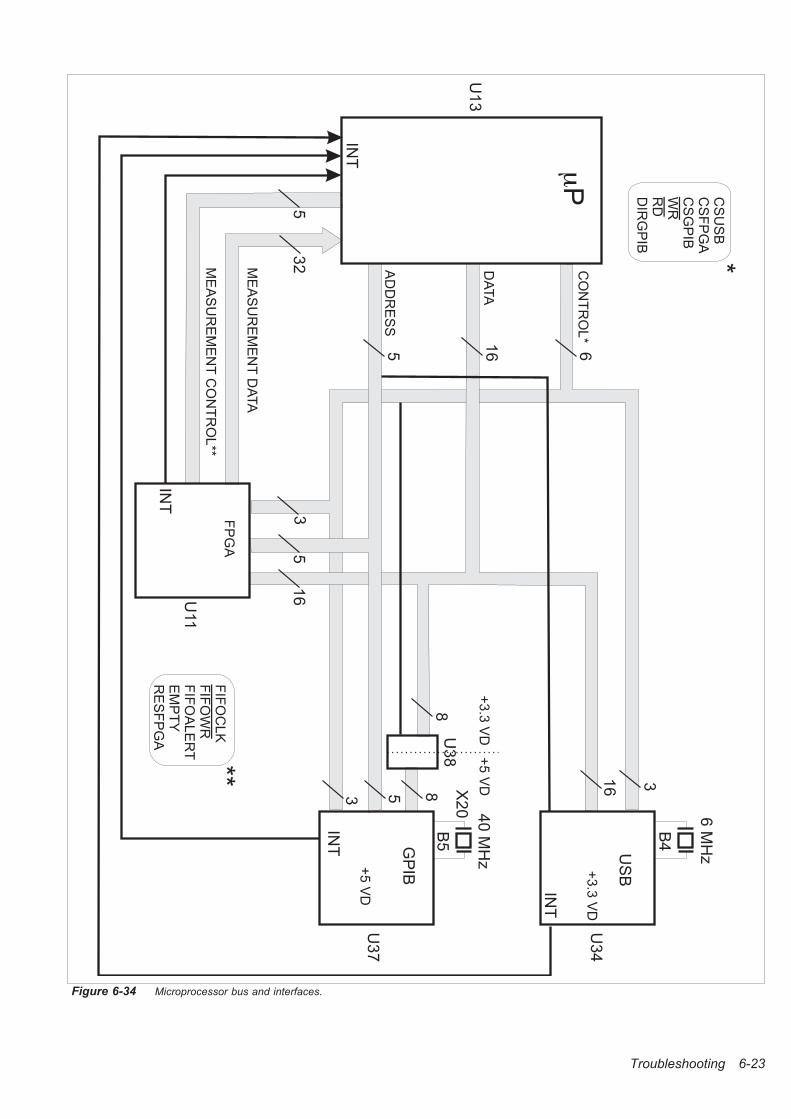
Troubleshooting 6-23
6M
Hz
B4
40
MH
z
B5G
PIB
U3
7
U3
4
US
B
�P
CO
NT
RO
L*
DA
TA
AD
DR
ES
S
FP
GA
+3
.3V
D
INT
+5
VD
INT
U3
8 +5
VD
+3.3
VD
88
3
3
16
16
16 6
35
55
53
2
INT
U11
X2
0
INT
U1
3
ME
AS
UR
EM
EN
TC
ON
TR
OL
**
ME
AS
UR
EM
EN
TD
ATA
FIF
OC
LK
FIF
OA
LE
RT
EM
PT
YR
ES
FP
GA
FIF
OW
R**
CS
US
BC
SF
PG
AC
SG
PIB
DIR
GP
IB
WR
RD
*
Figure 6-34 Microprocessor bus and interfaces.
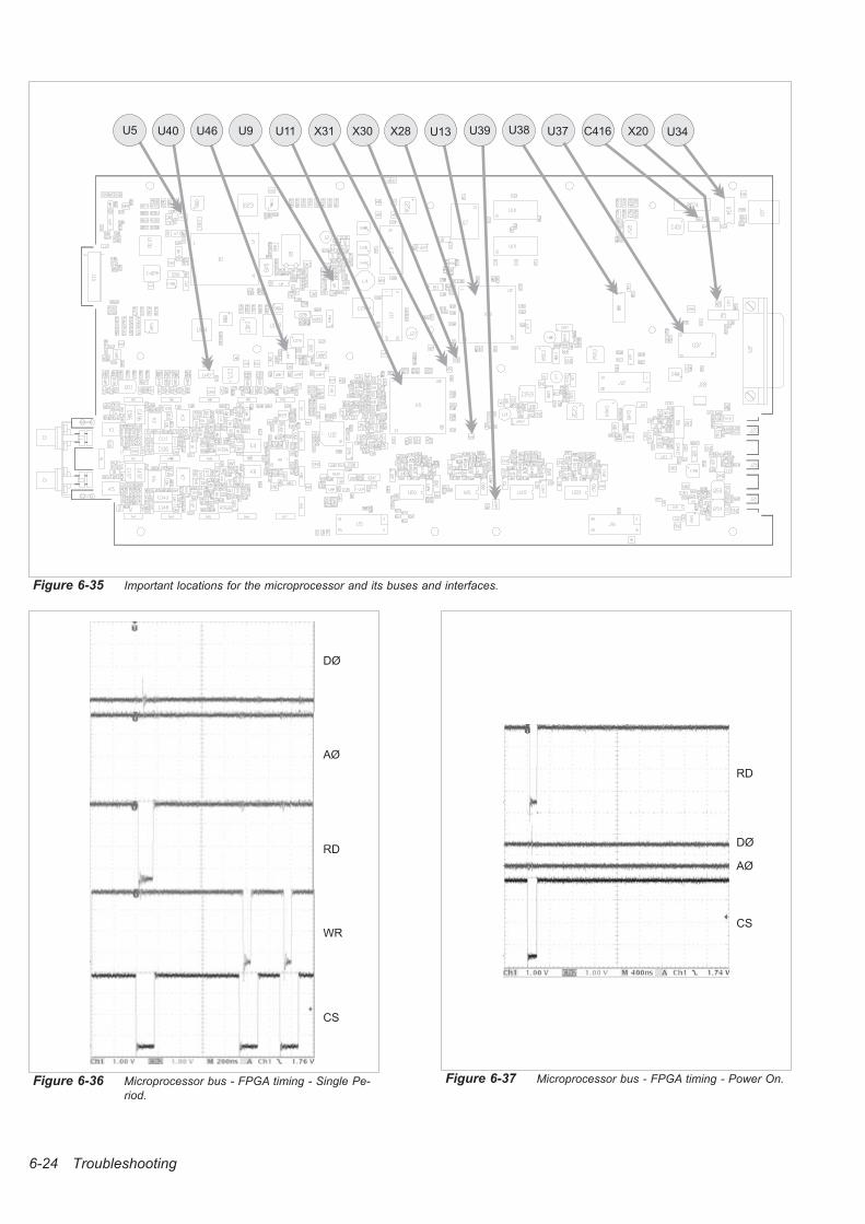
6-24 Troubleshooting
Figure 6-35 Important locations for the microprocessor and its buses and interfaces.
U5 U46 U9U40 X31 X30 X28 U39 U38 U37 C416 X20 U34U11 U13
Figure 6-36 Microprocessor bus - FPGA timing - Single Pe-
riod.
CS
WR
RD
AØ
DØ
Figure 6-37 Microprocessor bus - FPGA timing - Power On.
CS
AØ
DØ
RD
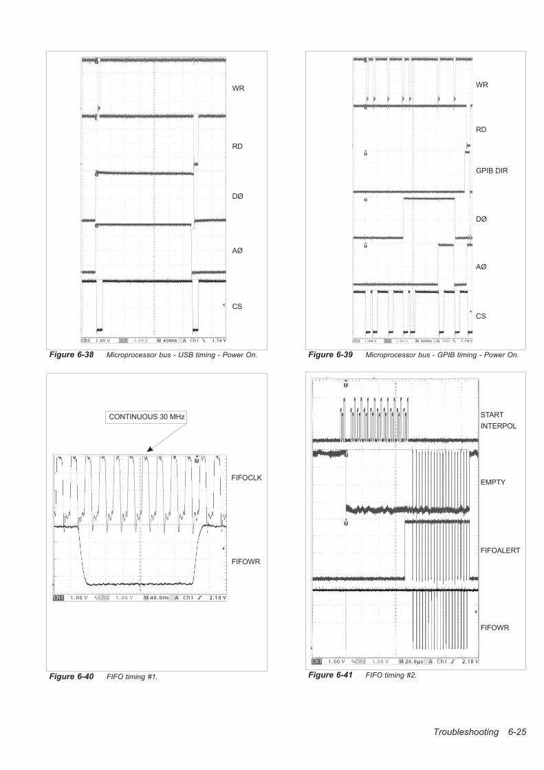
Troubleshooting 6-25
Figure 6-38 Microprocessor bus - USB timing - Power On.
CS
AØ
DØ
RD
WR
Figure 6-39 Microprocessor bus - GPIB timing - Power On.
GPIB DIR
CS
AØ
DØ
RD
WR
Figure 6-40 FIFO timing #1.
FIFOCLK
FIFOWR
CONTINUOUS 30 MHz
Figure 6-41 FIFO timing #2.
EMPTY
FIFOWR
FIFOALERT
START
INTERPOL
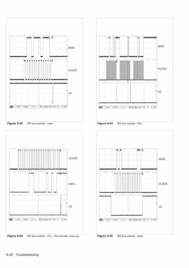
6-26 Troubleshooting
Figure 6-42 SPI bus activity - oven.
DATA
LD
CLOCK
Figure 6-43 SPI bus activity - PLL.
DATA
LD
CLOCK
Figure 6-44 SPI bus activity - PLL - first transfer close-up.
DATA
LD
CLOCK
Figure 6-45 SPI bus activity - trglvl.
DATA
LD
CLOCK
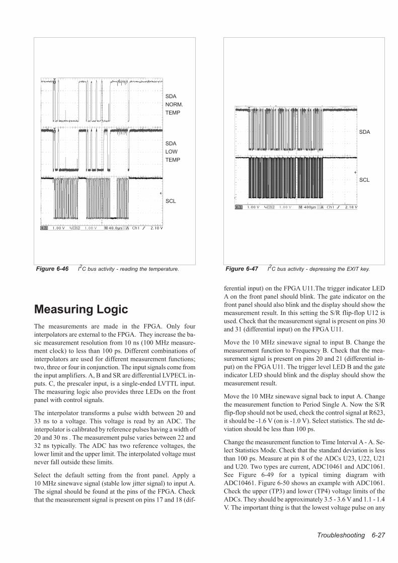
Measuring Logic
The measurements are made in the FPGA. Only four
interpolators are external to the FPGA. They increase the ba-
sic measurement resolution from 10 ns (100 MHz measure-
ment clock) to less than 100 ps. Different combinations of
interpolators are used for different measurement functions;
two, three or four in conjunction. The input signals come from
the input amplifiers. A, B and SR are differential LVPECL in-
puts. C, the prescaler input, is a single-ended LVTTL input.
The measuring logic also provides three LEDs on the front
panel with control signals.
The interpolator transforms a pulse width between 20 and
33 ns to a voltage. This voltage is read by an ADC. The
interpolator is calibrated by reference pulses having a width of
20 and 30 ns . The measurement pulse varies between 22 and
32 ns typically. The ADC has two reference voltages, the
lower limit and the upper limit. The interpolated voltage must
never fall outside these limits.
Select the default setting from the front panel. Apply a
10 MHz sinewave signal (stable low jitter signal) to input A.
The signal should be found at the pins of the FPGA. Check
that the measurement signal is present on pins 17 and 18 (dif-
ferential input) on the FPGA U11.The trigger indicator LED
A on the front panel should blink. The gate indicator on the
front panel should also blink and the display should show the
measurement result. In this setting the S/R flip-flop U12 is
used. Check that the measurement signal is present on pins 30
and 31 (differential input) on the FPGA U11.
Move the 10 MHz sinewave signal to input B. Change the
measurement function to Frequency B. Check that the mea-
surement signal is present on pins 20 and 21 (differential in-
put) on the FPGA U11. The trigger level LED B and the gate
indicator LED should blink and the display should show the
measurement result.
Move the 10 MHz sinewave signal back to input A. Change
the measurement function to Period Single A. Now the S/R
flip-flop should not be used, check the control signal at R623,
it should be -1.6 V (on is -1.0 V). Select statistics. The std de-
viation should be less than 100 ps.
Change the measurement function to Time Interval A - A. Se-
lect Statistics Mode. Check that the standard deviation is less
than 100 ps. Measure at pin 8 of the ADCs U23, U22, U21
and U20. Two types are current, ADC10461 and ADC1061.
See Figure 6-49 for a typical timing diagram with
ADC10461. Figure 6-50 shows an example with ADC1061.
Check the upper (TP3) and lower (TP4) voltage limits of the
ADCs. They should be approximately 3.5 - 3.6 V and 1.1 - 1.4
V. The important thing is that the lowest voltage pulse on any
Troubleshooting 6-27
Figure 6-46 I2C bus activity - reading the temperature.
SDA
NORM.
TEMP
SCL
SDA
LOW
TEMP
Figure 6-47 I2C bus activity - depressing the EXIT key.
SCL
SDA
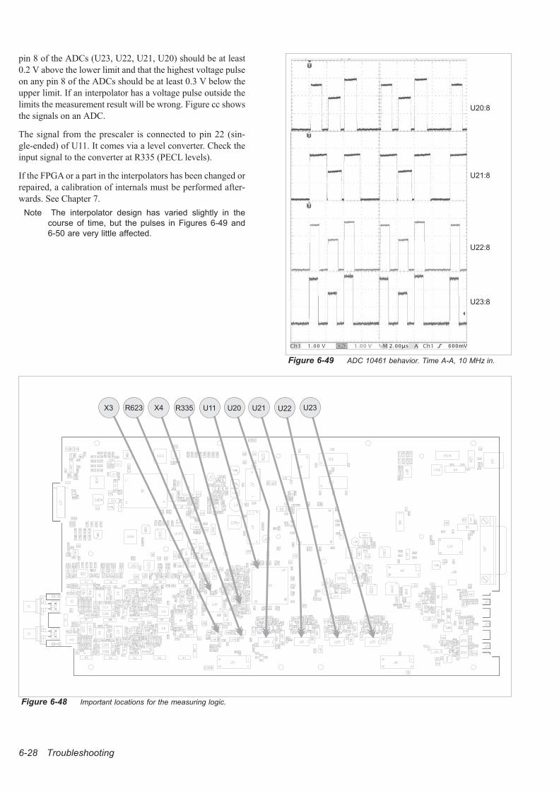
pin 8 of the ADCs (U23, U22, U21, U20) should be at least
0.2 V above the lower limit and that the highest voltage pulse
on any pin 8 of the ADCs should be at least 0.3 V below the
upper limit. If an interpolator has a voltage pulse outside the
limits the measurement result will be wrong. Figure cc shows
the signals on an ADC.
The signal from the prescaler is connected to pin 22 (sin-
gle-ended) of U11. It comes via a level converter. Check the
input signal to the converter at R335 (PECL levels).
If the FPGA or a part in the interpolators has been changed or
repaired, a calibration of internals must be performed after-
wards. See Chapter 7.
Note The interpolator design has varied slightly in the
course of time, but the pulses in Figures 6-49 and
6-50 are very little affected.
6-28 Troubleshooting
Figure 6-48 Important locations for the measuring logic.
R623 X4X3 U11 U20 U21 U23R335 U22
Figure 6-49 ADC 10461 behavior. Time A-A, 10 MHz in.
U21:8
U20:8
U22:8
U23:8
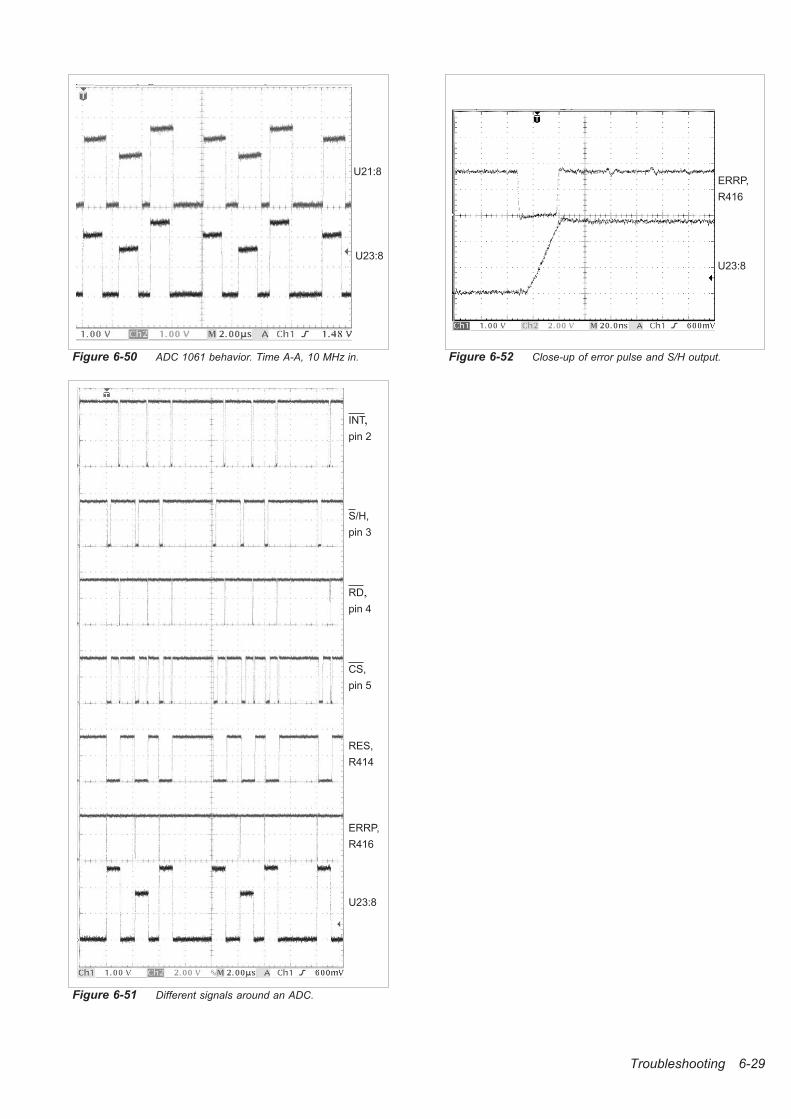
Troubleshooting 6-29
Figure 6-50 ADC 1061 behavior. Time A-A, 10 MHz in.
U23:8
U21:8
Figure 6-51 Different signals around an ADC.
U23:8
ERRP,
R416
RES,
R414
CS,
pin 5
RD,
pin 4
S/H,
pin 3
INT,
pin 2
Figure 6-52 Close-up of error pulse and S/H output.
U23:8
ERRP,
R416

6-30 Troubleshooting
U1
31
S/R
ON
/OF
F
EX
TA
RM
FP
GA
INP
UT
AM
PL
IFIE
RS
ET
C.
A B
S/R C
TR
GLV
LA
TR
GLV
LB
GA
TE
DIS
PL
AY
LE
DD
RIV
ER
S
INT
ER
PO
L0
INT
ER
PO
L1
INT
ER
PO
L2
INT
ER
PO
L3
U2
0
U2
1
U2
2
U2
3
ST
OP
STA
RT
Vre
f2
.5V
ref
U11
Figure 6-53 Measuring logic, block diagram.
Version B 6-31
Version B
The descriptions in this section apply to instru-
ments having a Sharp microprocessor.
See General Information on page III for details on
relevant serial numbers etc.
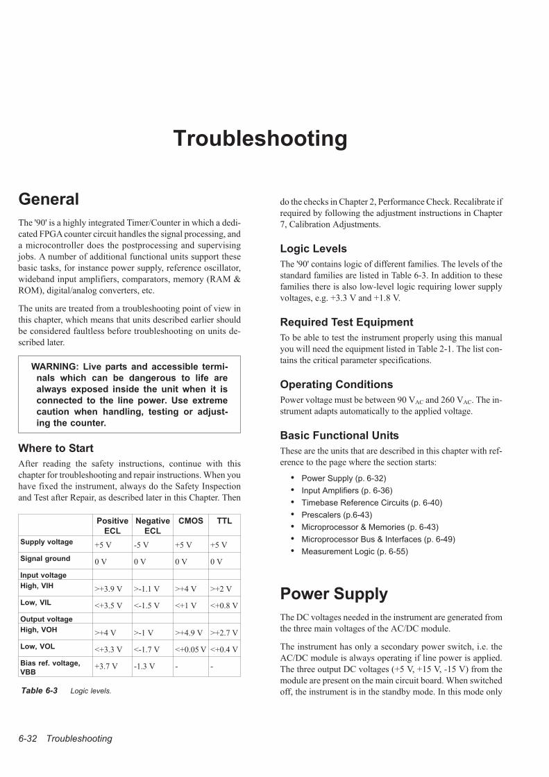
Troubleshooting
General
The '90' is a highly integrated Timer/Counter in which a dedi-
cated FPGA counter circuit handles the signal processing, and
a microcontroller does the postprocessing and supervising
jobs. A number of additional functional units support these
basic tasks, for instance power supply, reference oscillator,
wideband input amplifiers, comparators, memory (RAM &
ROM), digital/analog converters, etc.
The units are treated from a troubleshooting point of view in
this chapter, which means that units described earlier should
be considered faultless before troubleshooting on units de-
scribed later.
WARNING: Live parts and accessible termi-
nals which can be dangerous to life are
always exposed inside the unit when it is
connected to the line power. Use extreme
caution when handling, testing or adjust-
ing the counter.
Where to Start
After reading the safety instructions, continue with this
chapter for troubleshooting and repair instructions. When you
have fixed the instrument, always do the Safety Inspection
and Test after Repair, as described later in this Chapter. Then
do the checks in Chapter 2, Performance Check. Recalibrate if
required by following the adjustment instructions in Chapter
7, Calibration Adjustments.
Logic Levels
The '90' contains logic of different families. The levels of the
standard families are listed in Table 6-3. In addition to these
families there is also low-level logic requiring lower supply
voltages, e.g. +3.3 V and +1.8 V.
Required Test Equipment
To be able to test the instrument properly using this manual
you will need the equipment listed in Table 2-1. The list con-
tains the critical parameter specifications.
Operating Conditions
Power voltage must be between 90 VAC and 260 VAC. The in-
strument adapts automatically to the applied voltage.
Basic Functional Units
These are the units that are described in this chapter with ref-
erence to the page where the section starts:
• Power Supply (p. 6-32)
• Input Amplifiers (p. 6-36)
• Timebase Reference Circuits (p. 6-40)
• Prescalers (p.6-43)
• Microprocessor & Memories (p. 6-43)
• Microprocessor Bus & Interfaces (p. 6-49)
• Measurement Logic (p. 6-55)
Power Supply
The DC voltages needed in the instrument are generated from
the three main voltages of the AC/DC module.
The instrument has only a secondary power switch, i.e. the
AC/DC module is always operating if line power is applied.
The three output DC voltages (+5 V, +15 V, -15 V) from the
module are present on the main circuit board. When switched
off, the instrument is in the standby mode. In this mode only
6-32 Troubleshooting
Positive
ECL
Negative
ECL
CMOS TTL
Supply voltage +5 V -5 V +5 V +5 V
Signal ground 0 V 0 V 0 V 0 V
Input voltage
High, VIH >+3.9 V >-1.1 V >+4 V >+2 V
Low, VIL <+3.5 V <-1.5 V <+1 V <+0.8 V
Output voltage
High, VOH >+4 V >-1 V >+4.9 V >+2.7 V
Low, VOL <+3.3 V <-1.7 V <+0.05 V <+0.4 V
Bias ref. voltage,
VBB+3.7 V -1.3 V - -
Table 6-3 Logic levels.
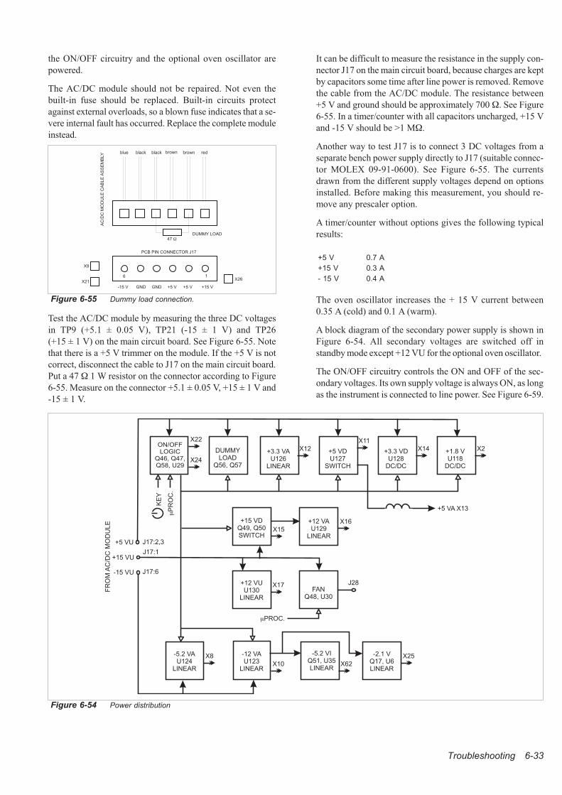
the ON/OFF circuitry and the optional oven oscillator are
powered.
The AC/DC module should not be repaired. Not even the
built-in fuse should be replaced. Built-in circuits protect
against external overloads, so a blown fuse indicates that a se-
vere internal fault has occurred. Replace the complete module
instead.
Test the AC/DC module by measuring the three DC voltages
in TP9 (+5.1 ± 0.05 V), TP21 (-15 ± 1 V) and TP26
(+15 ± 1 V) on the main circuit board. See Figure 6-55. Note
that there is a +5 V trimmer on the module. If the +5 V is not
correct, disconnect the cable to J17 on the main circuit board.
Put a 47 � 1 W resistor on the connector according to Figure
6-55. Measure on the connector +5.1 ± 0.05 V, +15 ± 1 V and
-15 ± 1 V.
It can be difficult to measure the resistance in the supply con-
nector J17 on the main circuit board, because charges are kept
by capacitors some time after line power is removed. Remove
the cable from the AC/DC module. The resistance between
+5 V and ground should be approximately 700 �. See Figure
6-55. In a timer/counter with all capacitors uncharged, +15 V
and -15 V should be >1 M�.
Another way to test J17 is to connect 3 DC voltages from a
separate bench power supply directly to J17 (suitable connec-
tor MOLEX 09-91-0600). See Figure 6-55. The currents
drawn from the different supply voltages depend on options
installed. Before making this measurement, you should re-
move any prescaler option.
A timer/counter without options gives the following typical
results:
+5 V 0.7 A
+15 V 0.3 A
- 15 V 0.4 A
The oven oscillator increases the + 15 V current between
0.35 A (cold) and 0.1 A (warm).
A block diagram of the secondary power supply is shown in
Figure 6-54. All secondary voltages are switched off in
standby mode except +12 VU for the optional oven oscillator.
The ON/OFF circuitry controls the ON and OFF of the sec-
ondary voltages. Its own supply voltage is always ON, as long
as the instrument is connected to line power. See Figure 6-59.
Troubleshooting 6-33
X2+1.8 VU118
DC/DC
+3.3 VDU128
DC/DC
+5 VDU127
SWITCH
X14
X11
+3.3 VAU126
LINEAR
X12DUMMYLOAD
Q56, Q57
ON/OFFLOGIC
Q46, Q47,Q58, U29
X22
X24
+12 VAU129
LINEAR
+15 VDQ49, Q50SWITCH
X15
+12 VUU130
LINEAR
X17FAN
Q48, U30
+15 VU
+5 VU
J28
X16
�PROC.
X10
-12 VAU123
LINEAR
-5.2 VAU124
LINEAR
X8
X62
X25
-15 VU
J17:2,3
J17:1
J17:6
FR
OM
AC
/DC
MO
DU
LE
+5 VA X13
�P
RO
C.
KE
Y
-5.2 VIQ51, U35LINEAR
-2.1 VQ17, U6LINEAR
Figure 6-54 Power distribution
47 �
redbrownbrownblackblackblue
AC
/DC
MO
DU
LE
CA
BL
EA
SS
EM
BLY
PCB PIN CONNECTOR J17
X26
X9
X21
+15 V+5 V+5 VGNDGND-15 V
DUMMY LOAD
16
Figure 6-55 Dummy load connection.
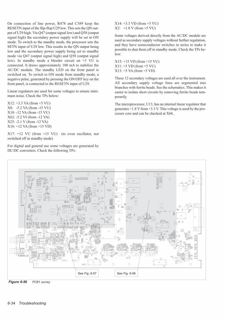
On connection of line power, R478 and C389 keep the
RESETN input of the flip-flop U29 low. This sets the QN out-
put of U29 high. Via Q47 (output signal low) and Q58 (output
signal high) the secondary power supply will be set in ON
mode. To switch to the standby mode, the processor sets the
SETN input of U29 low. This results in the QN output being
low and the secondary power supply being set to standby
mode via Q47 (output signal high) and Q58 (output signal
low). In standby mode a bleeder circuit on +5 VU is
connected. It draws approximately 100 mA to stabilize the
AC/DC module. The standby LED on the front panel is
switched on. To switch to ON mode from standby mode, a
negative pulse, generated by pressing the ON/OFF key on the
front panel, is connected to the RESETN input of U29.
Linear regulators are used for some voltages to ensure mini-
mum noise. Check the TPs below:
X12: +3.3 VA (from +5 VU)
X8: -5.2 VA (from -15 VU)
X10: -12 VA (from -15 VU)
X62: -5.2 VI (from -12 VA)
X25: -2.1 V (from -12 VA)
X16: +12 VA (from +15 VD)
X17: +12 VU (from +15 VU) (to oven oscillator, not
switched off in standby mode)
For digital and general use some voltages are generated by
DC/DC converters. Check the following TPs:
X14: +3.3 VD (from +5 VU)
X2: +1.8 V (from +5 VU)
Some voltages derived directly from the AC/DC module are
used as secondary supply voltages without further regulation,
and they have semiconductor switches in series to make it
possible to shut them off in standby mode. Check the TPs be-
low:
X15: +15 VD (from +15 VU)
X11: +5 VD (from +5 VU)
X13: +5 VA (from +5 VD)
These 12 secondary voltages are used all over the instrument.
All secondary supply voltage lines are segmented into
branches with ferrite beads. See the schematics. This makes it
easier to isolate short circuits by removing ferrite beads tem-
porarily.
The microprocessor, U13, has an internal linear regulator that
generates +1.8 V from +3.3 V. This voltage is used by the pro-
cessor core and can be checked at X66.
6-34 Troubleshooting
Figure 6-56 PCB1 survey
See Fig. 6-57 See Fig. 6-58
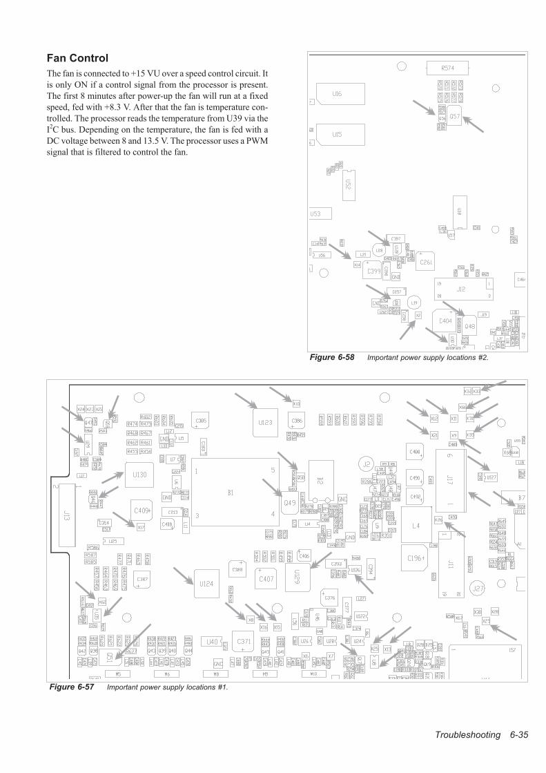
Troubleshooting 6-35
Fan Control
The fan is connected to +15 VU over a speed control circuit. It
is only ON if a control signal from the processor is present.
The first 8 minutes after power-up the fan will run at a fixed
speed, fed with +8.3 V. After that the fan is temperature con-
trolled. The processor reads the temperature from U39 via the
I2C bus. Depending on the temperature, the fan is fed with a
DC voltage between 8 and 13.5 V. The processor uses a PWM
signal that is filtered to control the fan.
Figure 6-57 Important power supply locations #1.
Figure 6-58 Important power supply locations #2.
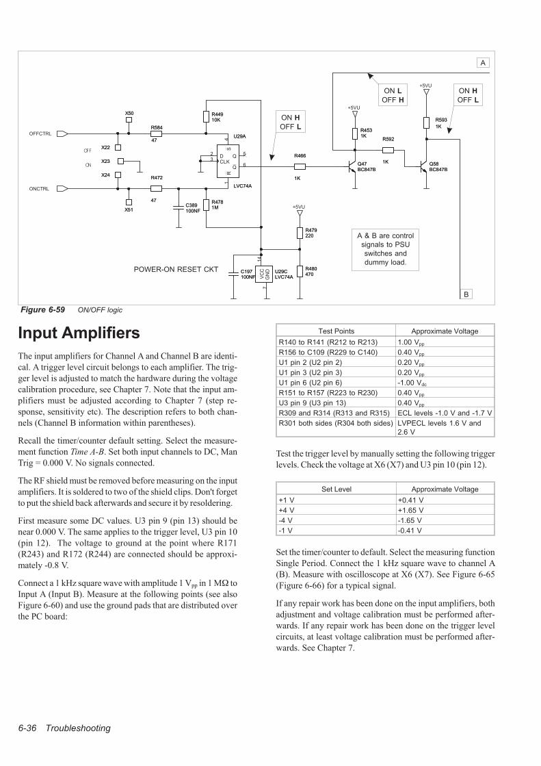
Input Amplifiers
The input amplifiers for Channel A and Channel B are identi-
cal. A trigger level circuit belongs to each amplifier. The trig-
ger level is adjusted to match the hardware during the voltage
calibration procedure, see Chapter 7. Note that the input am-
plifiers must be adjusted according to Chapter 7 (step re-
sponse, sensitivity etc). The description refers to both chan-
nels (Channel B information within parentheses).
Recall the timer/counter default setting. Select the measure-
ment function Time A-B. Set both input channels to DC, Man
Trig = 0.000 V. No signals connected.
The RF shield must be removed before measuring on the input
amplifiers. It is soldered to two of the shield clips. Don't forget
to put the shield back afterwards and secure it by resoldering.
First measure some DC values. U3 pin 9 (pin 13) should be
near 0.000 V. The same applies to the trigger level, U3 pin 10
(pin 12). The voltage to ground at the point where R171
(R243) and R172 (R244) are connected should be approxi-
mately -0.8 V.
Connect a 1 kHz square wave with amplitude 1 Vpp in 1 M� to
Input A (Input B). Measure at the following points (see also
Figure 6-60) and use the ground pads that are distributed over
the PC board:
Test Points Approximate Voltage
R140 to R141 (R212 to R213) 1.00 Vpp
R156 to C109 (R229 to C140) 0.40 Vpp
U1 pin 2 (U2 pin 2) 0.20 Vpp
U1 pin 3 (U2 pin 3) 0.20 Vpp
U1 pin 6 (U2 pin 6) -1.00 Vdc
R151 to R157 (R223 to R230) 0.40 Vpp
U3 pin 9 (U3 pin 13) 0.40 Vpp
R309 and R314 (R313 and R315) ECL levels -1.0 V and -1.7 V
R301 both sides (R304 both sides) LVPECL levels 1.6 V and
2.6 V
Test the trigger level by manually setting the following trigger
levels. Check the voltage at X6 (X7) and U3 pin 10 (pin 12).
Set Level Approximate Voltage
+1 V +0.41 V
+4 V +1.65 V
-4 V -1.65 V
-1 V -0.41 V
Set the timer/counter to default. Select the measuring function
Single Period. Connect the 1 kHz square wave to channel A
(B). Measure with oscilloscope at X6 (X7). See Figure 6-65
(Figure 6-66) for a typical signal.
If any repair work has been done on the input amplifiers, both
adjustment and voltage calibration must be performed after-
wards. If any repair work has been done on the trigger level
circuits, at least voltage calibration must be performed after-
wards. See Chapter 7.
6-36 Troubleshooting
+5VU
+5VU
+5VU
OFFCTRL
ONCTRL
ON
OFF
C389100NFC389100NF
R593
1K
R593
1K
R592
1K
R592
1K
R44910KR44910K
X51X51
Q58BC847BQ58BC847B
X22X22
X50X50
VC
C1
4
GN
D7
U29CLVC74AU29CLVC74A
R479220R479220
C197100NFC197100NF
R466
1K
R466
1KX24X24
Q47BC847BQ47BC847B
R472
47
R472
47
X23X23
R4531KR4531K
1MR4781MR478
R584
47
R584
47
D2
CLK3
S4
R1
Q5
Q6
U29A
LVC74A
U29A
LVC74A
R480470R480470
Figure 6-59 ON/OFF logic
ON H
OFF L
ON H
OFF L
ON L
OFF H
A & B are control
signals to PSU
switches and
dummy load.POWER-ON RESET CKT
A
B
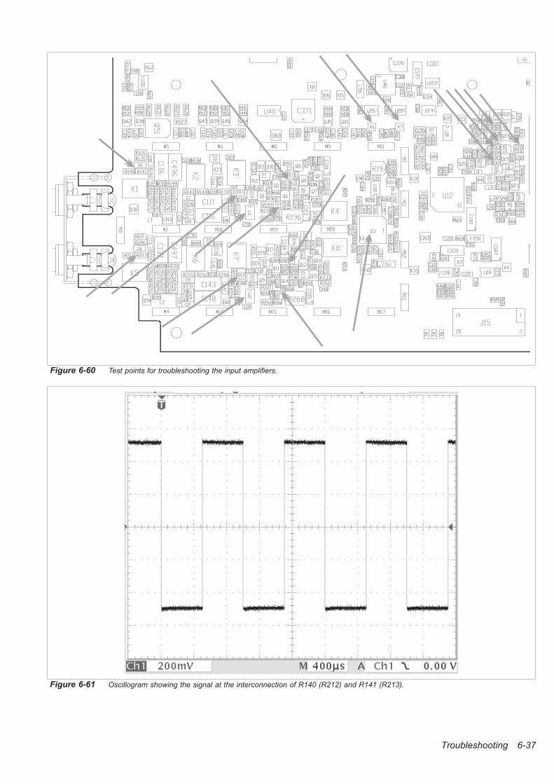
Troubleshooting 6-37
Figure 6-60 Test points for troubleshooting the input amplifiers.
Figure 6-61 Oscillogram showing the signal at the interconnection of R140 (R212) and R141 (R213).

6-38 Troubleshooting
Figure 6-62 Oscillogram showing the signal at the interconnection of R156 (R229) and C109 (C140).
Figure 6-63 Oscillogram showing the signal at U3:9 (U3:13).
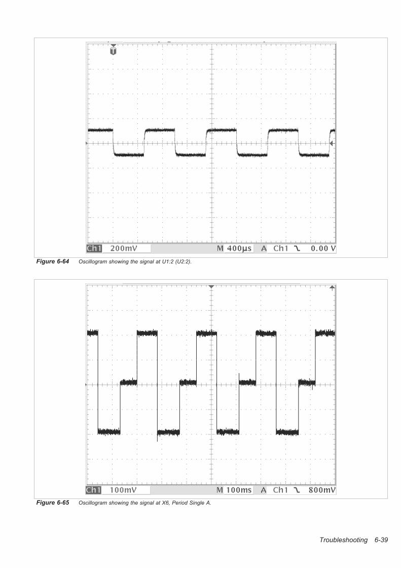
Troubleshooting 6-39
Figure 6-64 Oscillogram showing the signal at U1:2 (U2:2).
Figure 6-65 Oscillogram showing the signal at X6, Period Single A.
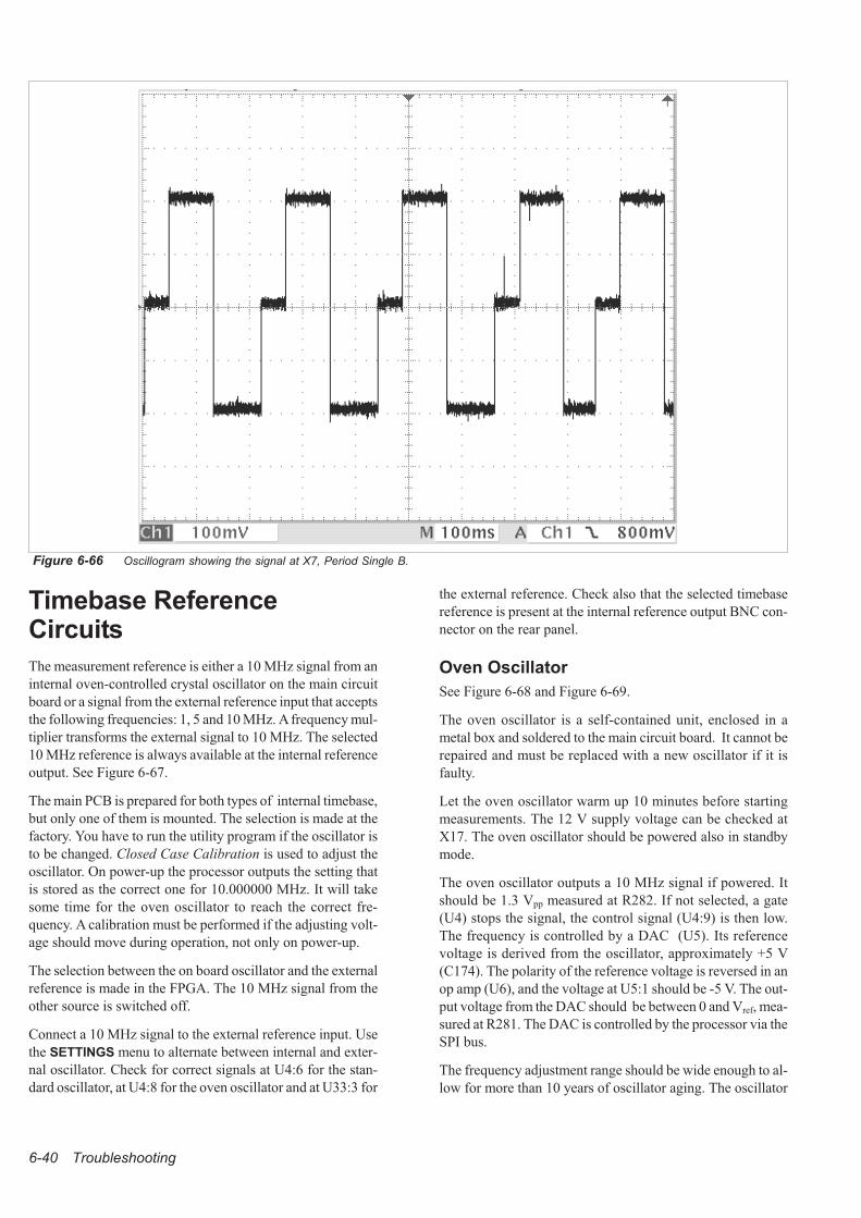
Timebase ReferenceCircuits
The measurement reference is either a 10 MHz signal from an
internal oven-controlled crystal oscillator on the main circuit
board or a signal from the external reference input that accepts
the following frequencies: 1, 5 and 10 MHz. Afrequency mul-
tiplier transforms the external signal to 10 MHz. The selected
10 MHz reference is always available at the internal reference
output. See Figure 6-67.
The main PCB is prepared for both types of internal timebase,
but only one of them is mounted. The selection is made at the
factory. You have to run the utility program if the oscillator is
to be changed. Closed Case Calibration is used to adjust the
oscillator. On power-up the processor outputs the setting that
is stored as the correct one for 10.000000 MHz. It will take
some time for the oven oscillator to reach the correct fre-
quency. A calibration must be performed if the adjusting volt-
age should move during operation, not only on power-up.
The selection between the on board oscillator and the external
reference is made in the FPGA. The 10 MHz signal from the
other source is switched off.
Connect a 10 MHz signal to the external reference input. Use
the SETTINGS menu to alternate between internal and exter-
nal oscillator. Check for correct signals at U4:6 for the stan-
dard oscillator, at U4:8 for the oven oscillator and at U33:3 for
the external reference. Check also that the selected timebase
reference is present at the internal reference output BNC con-
nector on the rear panel.
Oven Oscillator
See Figure 6-68 and Figure 6-69.
The oven oscillator is a self-contained unit, enclosed in a
metal box and soldered to the main circuit board. It cannot be
repaired and must be replaced with a new oscillator if it is
faulty.
Let the oven oscillator warm up 10 minutes before starting
measurements. The 12 V supply voltage can be checked at
X17. The oven oscillator should be powered also in standby
mode.
The oven oscillator outputs a 10 MHz signal if powered. It
should be 1.3 Vpp measured at R282. If not selected, a gate
(U4) stops the signal, the control signal (U4:9) is then low.
The frequency is controlled by a DAC (U5). Its reference
voltage is derived from the oscillator, approximately +5 V
(C174). The polarity of the reference voltage is reversed in an
op amp (U6), and the voltage at U5:1 should be -5 V. The out-
put voltage from the DAC should be between 0 and Vref, mea-
sured at R281. The DAC is controlled by the processor via the
SPI bus.
The frequency adjustment range should be wide enough to al-
low for more than 10 years of oscillator aging. The oscillator
6-40 Troubleshooting
Figure 6-66 Oscillogram showing the signal at X7, Period Single B.
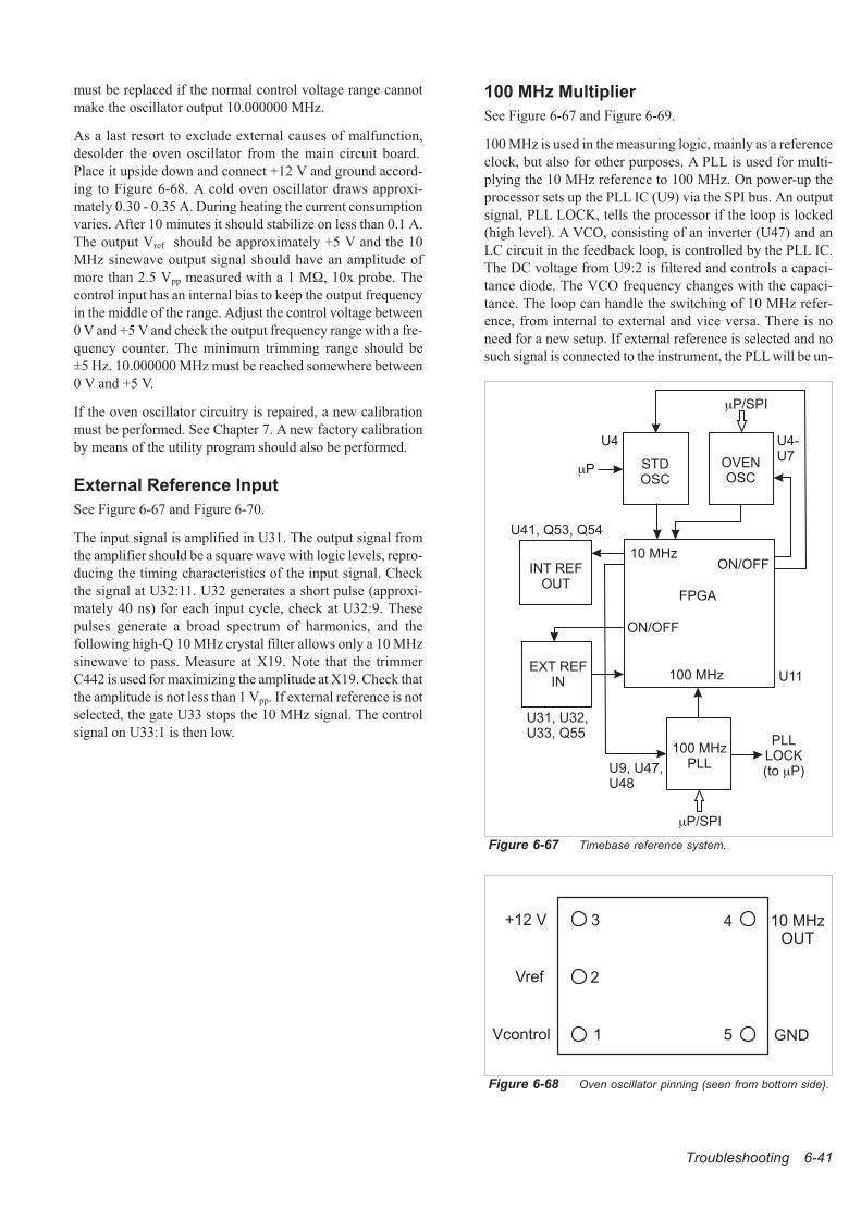
Troubleshooting 6-41
must be replaced if the normal control voltage range cannot
make the oscillator output 10.000000 MHz.
As a last resort to exclude external causes of malfunction,
desolder the oven oscillator from the main circuit board.
Place it upside down and connect +12 V and ground accord-
ing to Figure 6-68. A cold oven oscillator draws approxi-
mately 0.30 - 0.35 A. During heating the current consumption
varies. After 10 minutes it should stabilize on less than 0.1 A.
The output Vref should be approximately +5 V and the 10
MHz sinewave output signal should have an amplitude of
more than 2.5 Vpp measured with a 1 M�, 10x probe. The
control input has an internal bias to keep the output frequency
in the middle of the range. Adjust the control voltage between
0 V and +5 V and check the output frequency range with a fre-
quency counter. The minimum trimming range should be
±5 Hz. 10.000000 MHz must be reached somewhere between
0 V and +5 V.
If the oven oscillator circuitry is repaired, a new calibration
must be performed. See Chapter 7. A new factory calibration
by means of the utility program should also be performed.
External Reference Input
See Figure 6-67 and Figure 6-70.
The input signal is amplified in U31. The output signal from
the amplifier should be a square wave with logic levels, repro-
ducing the timing characteristics of the input signal. Check
the signal at U32:11. U32 generates a short pulse (approxi-
mately 40 ns) for each input cycle, check at U32:9. These
pulses generate a broad spectrum of harmonics, and the
following high-Q 10 MHz crystal filter allows only a 10 MHz
sinewave to pass. Measure at X19. Note that the trimmer
C442 is used for maximizing the amplitude at X19. Check that
the amplitude is not less than 1 Vpp. If external reference is not
selected, the gate U33 stops the 10 MHz signal. The control
signal on U33:1 is then low.
100 MHz Multiplier
See Figure 6-67 and Figure 6-69.
100 MHz is used in the measuring logic, mainly as a reference
clock, but also for other purposes. A PLL is used for multi-
plying the 10 MHz reference to 100 MHz. On power-up the
processor sets up the PLL IC (U9) via the SPI bus. An output
signal, PLL LOCK, tells the processor if the loop is locked
(high level). A VCO, consisting of an inverter (U47) and an
LC circuit in the feedback loop, is controlled by the PLL IC.
The DC voltage from U9:2 is filtered and controls a capaci-
tance diode. The VCO frequency changes with the capaci-
tance. The loop can handle the switching of 10 MHz refer-
ence, from internal to external and vice versa. There is no
need for a new setup. If external reference is selected and no
such signal is connected to the instrument, the PLL will be un-
FPGA
100 MHzPLL
EXT REFIN
INT REFOUT
STDOSC
OVENOSC
U4 U4-U7
10 MHz
U11
ON/OFF
100 MHz
PLLLOCK(to �P)
ON/OFF
�P/SPI
�P
�P/SPI
U41, Q53, Q54
U31, U32,U33, Q55
U9, U47,U48
Figure 6-67 Timebase reference system.
3
2
1 5
4+12 V
Vref
Vcontrol GND
10 MHzOUT
Figure 6-68 Oven oscillator pinning (seen from bottom side).
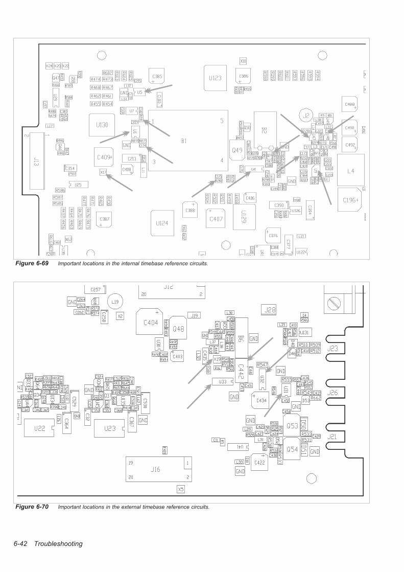
6-42 Troubleshooting
Figure 6-69 Important locations in the internal timebase reference circuits.
Figure 6-70 Important locations in the external timebase reference circuits.
Troubleshooting 6-43
locked, and the VCO will go to one of the extremes. The typi-
cal range of the VCO is 95 to 105 MHz, thus giving an error of
typically 5 % in the measuring results.
Check the loop voltage (DC) at R272. It should be 1.6 - 2.2 V.
Check the 100 MHz signal at U48:4. It should be locked to the
incoming 10 MHz at U9:8. Check the lock condition with a
2-channel oscilloscope. Trigger on the 10 MHz channel. Then
the signal on the other channel shall be fixed, i.e. not moving
along the time axis. Check the PLL LOCK signal at U9:14
(lock is high).
Prescaler
The optional prescalers are not to be repaired. The faulty unit
should be sent to the factory, and an exchange unit will be
returned.
The best way to isolate the fault is to use another, functioning,
timer/counter with the same prescaler. Interchange the
prescalers and see if the problem follows the prescaler or the
timer/counter.
First measure with Channels A and B and check that the result
is OK. Select the function Frequency C. Connect a signal ac-
cording to Table 6-2 to Input C. Check the following pins on
the prescaler connector J15 on the main circuit board.
Pin 1 +5 V supply
Pin 5 +12 V supply
Pin 7 ON/OFF, ON is 0 V
Pin 11 test signal, should be 0 V
Pin 12 code 0, see Table 6-2
Pin 14 code 1, see Table 6-2
Pin 16 code 2, see Table 6-2
Pin 4 prescaler output signal, PECL levels (+4.1 V and
+3.4 V)
Measure with oscilloscope and probe at pin 4. The output fre-
quency should be the input frequency divided by the factor in
the table. Check with a frequency counter.
Note: The 2.7 GHz option has a sensitivity trimmer. See
page 7-14 for information on how to adjust it.
Microprocessor & Memories
Startup Process
The processor in this instrument is a Sharp LH79524 with a
32-bit ARM720T core. It is housed in an IC (U13) together
with peripheral units like SRAM, timers, I2C bus interface,
SPI bus interface and LCD controller.
The 32-bit microprocessor bus is connected to one 16-bit
Flash PROM (U17) and two 16-bit SDRAMs (U15 & U16).
The two SDRAMs are organized as one 32-bit wide memory.
The microprocessor bus is also, via bidirectional buffers, con-
nected to an FPGA, a USB IC and a GPIB IC.
A reset IC (U116) monitors +3.3 VD and +1.8 V. The reset
signal is active low and is kept low for approximately 160 to
180 ms after the voltages have settled and been approved.
Measure at X33. The ramp-up time for +3.3 VD is approxi-
mately 3 ms.
The processor has an internal linear regulator that generates
the core voltage (+1.8 V) from the +3.3 VD I/O voltage.
Check +1.8 V at X66.
The rising edge of the reset signal marks the start of the boot
sequence. All I/Os on the processor are set to inputs. The
11.2896 MHz oscillator will start running (check at R358).
An internal PLL generates 1.88 MHz (reset value) as micro-
processor clock (check at X29). The processor will start read-
ing in the Flash PROM. The initializing of the processor and
the peripherals will start.
The I/Os will be set up, the processor clock will be set to
50.8 MHz (check at X29). The SDRAMs will start, and the
code is copied from the Flash PROM to the SDRAMs. From
now on the code is executed from the SDRAMs. Then all the
other subsystems are initialized: I2C bus, LCD controller, SPI
bus, fan etc. The FPGAis also programmed by the processor.
The progress of the initialization can be followed at two test
points, X55 and X31.
Test Point Reset I/O
Setup
SDRAM
Execute
I2C Init Init Ready
X55 float. inp. 1 0 1 0
X31 float. inp. 1 1 0 0
See Figures 6-74 to 6-76 for a survey of a typical instrument
startup.
The LCD is switched on. The LCD controller in the processor
generates the control signals for the LCD. See Figures 6-77 to
6-81and 6-83. Note the different timing for the signals. The
I2C bus is used for switching the LCD on. The ON signal can
be checked at R34 on the display board. It should be high. The
LCD voltages must also be switched on. It is done by a control
signal from the processor. Check the signal at R33 on the dis-
play board. It should be high. Negative pulses on this signal
are used for adjusting the contrast of the LCD, i.e. the LCD
PRESCALER 2.7 GHz
Frequency (GHz) 1
Level (dBm) 0
Division Factor 16
Code 0 0
Code 1 1
Code 2 0
Table 6-4 Prescaler characteristics.
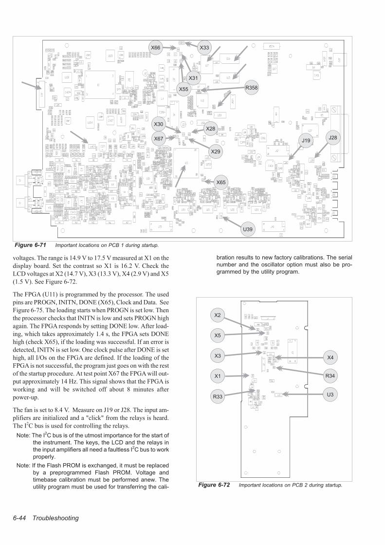
voltages. The range is 14.9 V to 17.5 V measured at X1 on the
display board. Set the contrast so X1 is 16.2 V. Check the
LCD voltages at X2 (14.7 V), X3 (13.3 V), X4 (2.9 V) and X5
(1.5 V). See Figure 6-72.
The FPGA (U11) is programmed by the processor. The used
pins are PROGN, INITN, DONE (X65), Clock and Data. See
Figure 6-75. The loading starts when PROGN is set low. Then
the processor checks that INITN is low and sets PROGN high
again. The FPGA responds by setting DONE low. After load-
ing, which takes approximately 1.4 s, the FPGA sets DONE
high (check X65), if the loading was successful. If an error is
detected, INITN is set low. One clock pulse after DONE is set
high, all I/Os on the FPGA are defined. If the loading of the
FPGA is not successful, the program just goes on with the rest
of the startup procedure. At test point X67 the FPGA will out-
put approximately 14 Hz. This signal shows that the FPGA is
working and will be switched off about 8 minutes after
power-up.
The fan is set to 8.4 V. Measure on J19 or J28. The input am-
plifiers are initialized and a "click" from the relays is heard.
The I2C bus is used for controlling the relays.
Note: The I2C bus is of the utmost importance for the start of
the instrument. The keys, the LCD and the relays in
the input amplifiers all need a faultless I2C bus to work
properly.
Note: If the Flash PROM is exchanged, it must be replaced
by a preprogrammed Flash PROM. Voltage and
timebase calibration must be performed anew. The
utility program must be used for transferring the cali-
bration results to new factory calibrations. The serial
number and the oscillator option must also be pro-
grammed by the utility program.
6-44 Troubleshooting
Figure 6-71 Important locations on PCB 1 during startup.
J19J28
U39
X33X66
X31
X55
X67
X30X28
X29
X65
R358
Figure 6-72 Important locations on PCB 2 during startup.
X3
X2
X5
X1
R33 U3
R34
X4
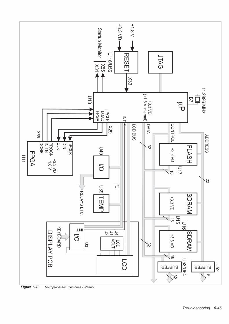
Troubleshooting 6-45
JTA
G
RE
SE
T+
1.8
V
+3.3
VD
X3
3
11.2
89
6M
Hz
�P
B7
FLA
SH
SD
RA
MS
DR
AM
AD
DR
ES
S
CO
NT
RO
L
U11
6/U
55
U1
3
DIS
PL
AY
PC
B
FP
GA
DA
TA
LC
DB
US
LC
DV
OLT
U1
7U
15 U
16
U4
U1
U2
LC
D
I/O
U3
KE
YB
OA
RD
U11
TE
MP
U3
9
IC 2
I/OU
40
INT
INT
RE
LA
YS
ET
C.
�P
CL
K
�P
CL
KL
OA
DF
PG
A
CL
K
X2
9
+3
.3V
D(+
1.8
Vin
tern
al)
+3
.3V
D+
1.8
V
+3
.3V
D+
3.3
VD
+3
.3V
D
22
16
16
16
32
DIN
X5
5
X3
1S
tartu
pM
on
itor
DO
NE
INIT
NP
RO
GN
X6
5
BUFFER
5
32
32
BUFFER
U1
6
U5
2
U5
3/U
54
Figure 6-73 Microprocessor, memories - startup.
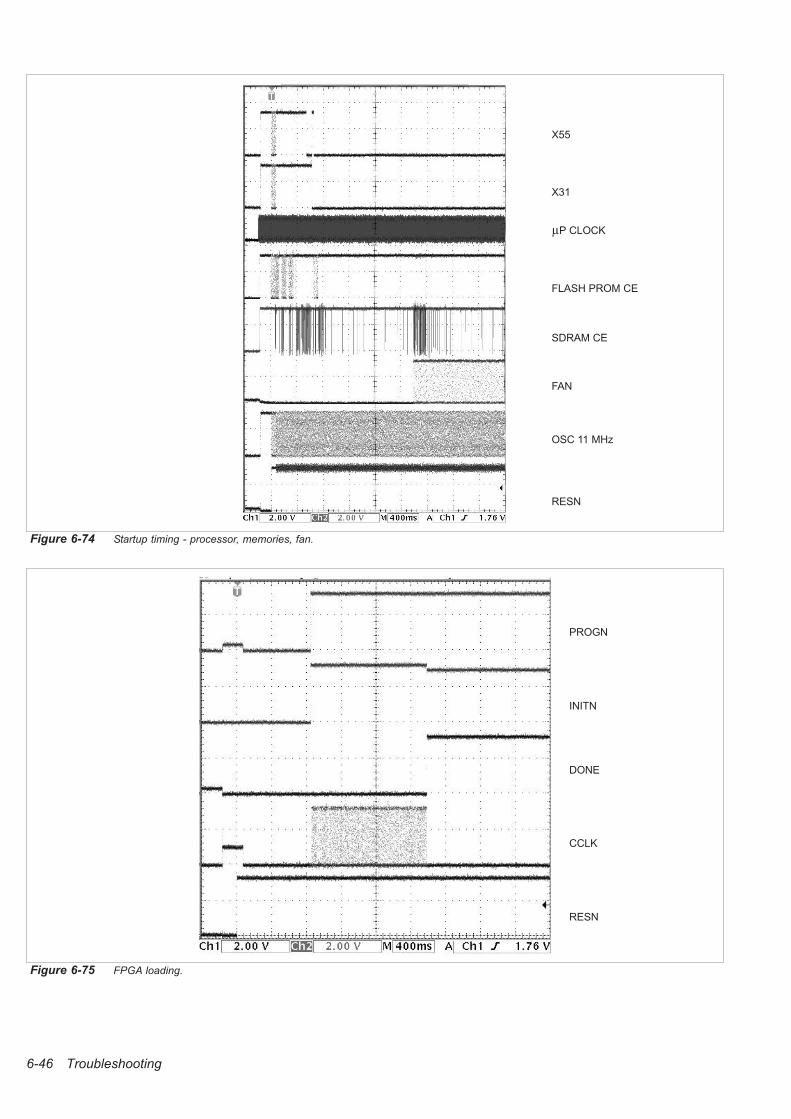
6-46 Troubleshooting
Figure 6-74 Startup timing - processor, memories, fan.
RESN
FAN
SDRAM CE
FLASH PROM CE
µP CLOCK
OSC 11 MHz
X31
X55
Figure 6-75 FPGA loading.
PROGN
INITN
DONE
CCLK
RESN
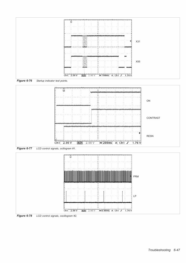
Troubleshooting 6-47
Figure 6-76 Startup indicator test points.
Figure 6-77 LCD control signals, ocillogram #1.
ON
CONTRAST
RESN
Figure 6-78 LCD control signals, oscillogram #2.
FRM
LP
X55
X31
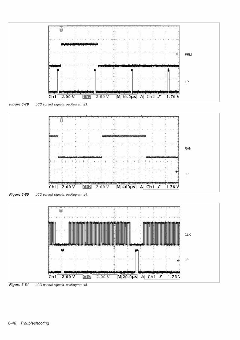
6-48 Troubleshooting
Figure 6-79 LCD control signals, oscillogram #3.
FRM
LP
Figure 6-80 LCD control signals, oscillogram #4.
LP
RAN
Figure 6-81 LCD control signals, oscillogram #5.
LP
CLK
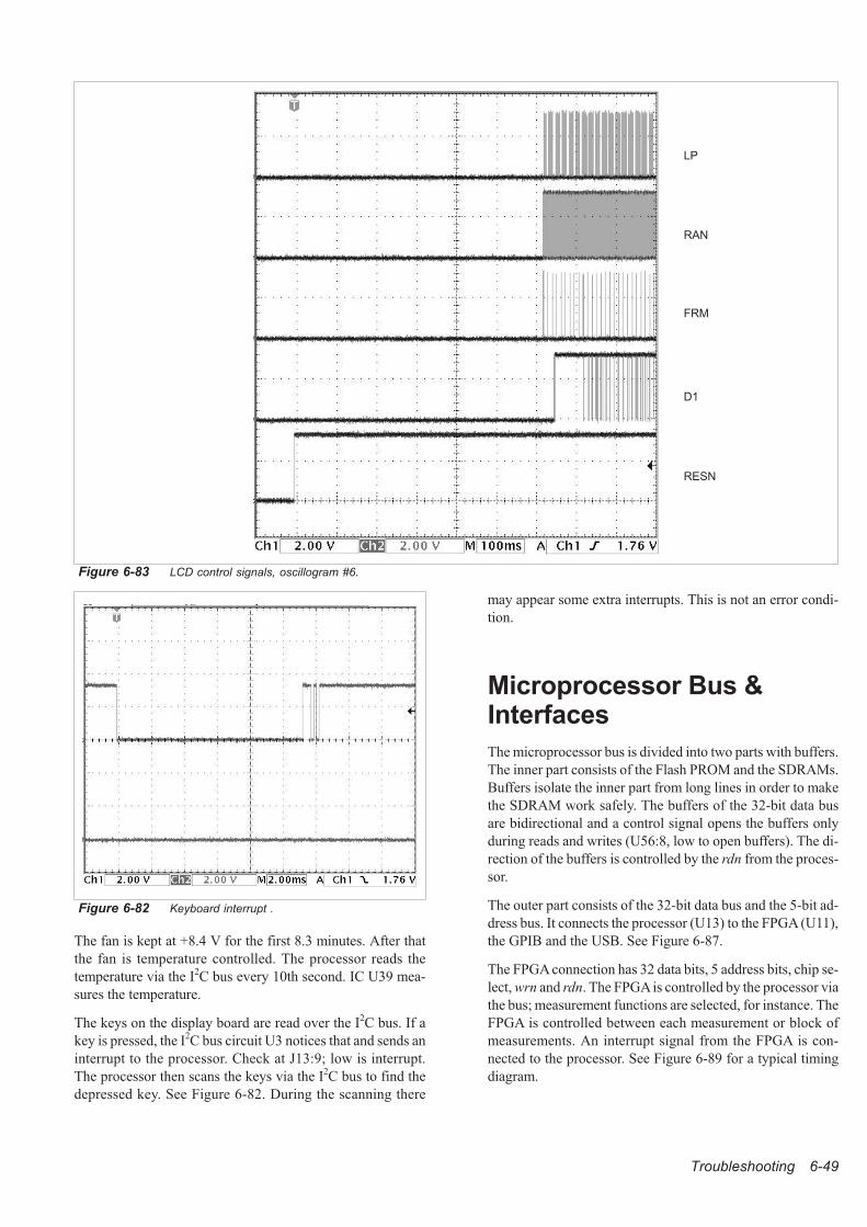
Troubleshooting 6-49
The fan is kept at +8.4 V for the first 8.3 minutes. After that
the fan is temperature controlled. The processor reads the
temperature via the I2C bus every 10th second. IC U39 mea-
sures the temperature.
The keys on the display board are read over the I2C bus. If a
key is pressed, the I2C bus circuit U3 notices that and sends an
interrupt to the processor. Check at J13:9; low is interrupt.
The processor then scans the keys via the I2C bus to find the
depressed key. See Figure 6-82. During the scanning there
may appear some extra interrupts. This is not an error condi-
tion.
Microprocessor Bus &Interfaces
The microprocessor bus is divided into two parts with buffers.
The inner part consists of the Flash PROM and the SDRAMs.
Buffers isolate the inner part from long lines in order to make
the SDRAM work safely. The buffers of the 32-bit data bus
are bidirectional and a control signal opens the buffers only
during reads and writes (U56:8, low to open buffers). The di-
rection of the buffers is controlled by the rdn from the proces-
sor.
The outer part consists of the 32-bit data bus and the 5-bit ad-
dress bus. It connects the processor (U13) to the FPGA (U11),
the GPIB and the USB. See Figure 6-87.
The FPGA connection has 32 data bits, 5 address bits, chip se-
lect, wrn and rdn. The FPGAis controlled by the processor via
the bus; measurement functions are selected, for instance. The
FPGA is controlled between each measurement or block of
measurements. An interrupt signal from the FPGA is con-
nected to the processor. See Figure 6-89 for a typical timing
diagram.
Figure 6-82 Keyboard interrupt .
Figure 6-83 LCD control signals, oscillogram #6.
LP
RESN
RAN
FRM
D1
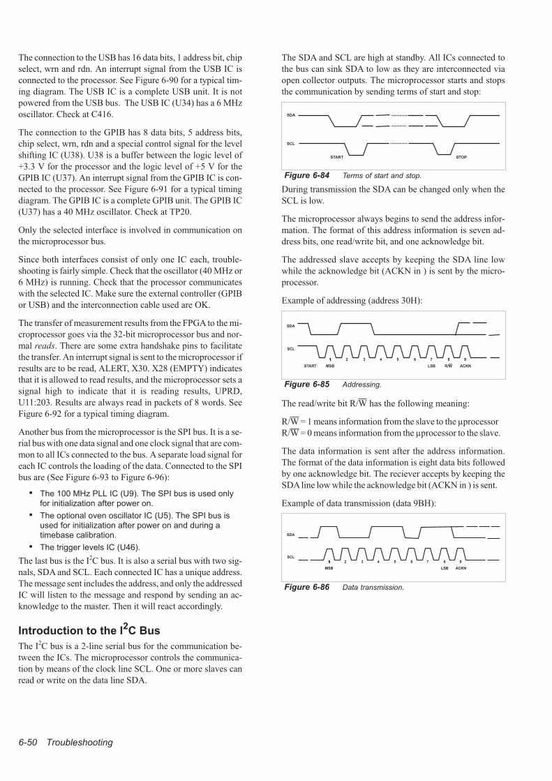
The connection to the USB has 16 data bits, 1 address bit, chip
select, wrn and rdn. An interrupt signal from the USB IC is
connected to the processor. See Figure 6-90 for a typical tim-
ing diagram. The USB IC is a complete USB unit. It is not
powered from the USB bus. The USB IC (U34) has a 6 MHz
oscillator. Check at C416.
The connection to the GPIB has 8 data bits, 5 address bits,
chip select, wrn, rdn and a special control signal for the level
shifting IC (U38). U38 is a buffer between the logic level of
+3.3 V for the processor and the logic level of +5 V for the
GPIB IC (U37). An interrupt signal from the GPIB IC is con-
nected to the processor. See Figure 6-91 for a typical timing
diagram. The GPIB IC is a complete GPIB unit. The GPIB IC
(U37) has a 40 MHz oscillator. Check at TP20.
Only the selected interface is involved in communication on
the microprocessor bus.
Since both interfaces consist of only one IC each, trouble-
shooting is fairly simple. Check that the oscillator (40 MHz or
6 MHz) is running. Check that the processor communicates
with the selected IC. Make sure the external controller (GPIB
or USB) and the interconnection cable used are OK.
The transfer of measurement results from the FPGA to the mi-
croprocessor goes via the 32-bit microprocessor bus and nor-
mal reads. There are some extra handshake pins to facilitate
the transfer. An interrupt signal is sent to the microprocessor if
results are to be read, ALERT, X30. X28 (EMPTY) indicates
that it is allowed to read results, and the microprocessor sets a
signal high to indicate that it is reading results, UPRD,
U11:203. Results are always read in packets of 8 words. See
Figure 6-92 for a typical timing diagram.
Another bus from the microprocessor is the SPI bus. It is a se-
rial bus with one data signal and one clock signal that are com-
mon to all ICs connected to the bus. A separate load signal for
each IC controls the loading of the data. Connected to the SPI
bus are (See Figure 6-93 to Figure 6-96):
• The 100 MHz PLL IC (U9). The SPI bus is used onlyfor initialization after power on.
• The optional oven oscillator IC (U5). The SPI bus isused for initialization after power on and during atimebase calibration.
• The trigger levels IC (U46).
The last bus is the I2C bus. It is also a serial bus with two sig-
nals, SDA and SCL. Each connected IC has a unique address.
The message sent includes the address, and only the addressed
IC will listen to the message and respond by sending an ac-
knowledge to the master. Then it will react accordingly.
Introduction to the I2C Bus
The I2C bus is a 2-line serial bus for the communication be-
tween the ICs. The microprocessor controls the communica-
tion by means of the clock line SCL. One or more slaves can
read or write on the data line SDA.
The SDA and SCL are high at standby. All ICs connected to
the bus can sink SDA to low as they are interconnected via
open collector outputs. The microprocessor starts and stops
the communication by sending terms of start and stop:
During transmission the SDA can be changed only when the
SCL is low.
The microprocessor always begins to send the address infor-
mation. The format of this address information is seven ad-
dress bits, one read/write bit, and one acknowledge bit.
The addressed slave accepts by keeping the SDA line low
while the acknowledge bit (ACKN in ) is sent by the micro-
processor.
Example of addressing (address 30H):
The read/write bit R/W has the following meaning:
R/W = 1 means information from the slave to the µprocessor
R/W = 0 means information from the µprocessor to the slave.
The data information is sent after the address information.
The format of the data information is eight data bits followed
by one acknowledge bit. The reciever accepts by keeping the
SDAline low while the acknowledge bit (ACKN in ) is sent.
Example of data transmission (data 9BH):
6-50 Troubleshooting
START STOP
SDA
SCL
Figure 6-84 Terms of start and stop.
SDA
SCL
START MSB LSB ACKNR/W
1 2 3 4 51 61 7 8 9
Figure 6-85 Addressing.
SDA
SCL
MSB LSB ACKN
1 2 3 4 51 61 7 8 9
Figure 6-86 Data transmission.
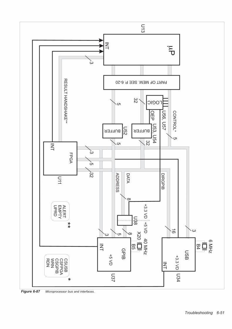
Troubleshooting 6-51
6M
Hz
B4
40
MH
z
B5G
PIB
U3
7
U3
4
US
B
�P
CO
NT
RO
L*
DA
TA
AD
DR
ES
S
FP
GA
+3.3
VD
INT
+5
VD
INT
U3
8 +5
VD
+3.3
VD
88
3
3
16
32
32
5
35
55
3
INT
U11
X2
0
INT
U1
3
RE
SU
LT
HA
ND
SH
AK
E**
AL
ER
TE
MP
TY
UP
RD
**C
SU
SB
CS
FP
GA
CS
GP
IBW
RN
RD
N
*
PARTOFMEM.SEEP.6-20
DIR
GP
IB
U5
2
U5
3,U
54
BUFFERBUFFER
LOGIC
U5
6,U
57
OE
P
32
5
Figure 6-87 Microprocessor bus and interfaces.
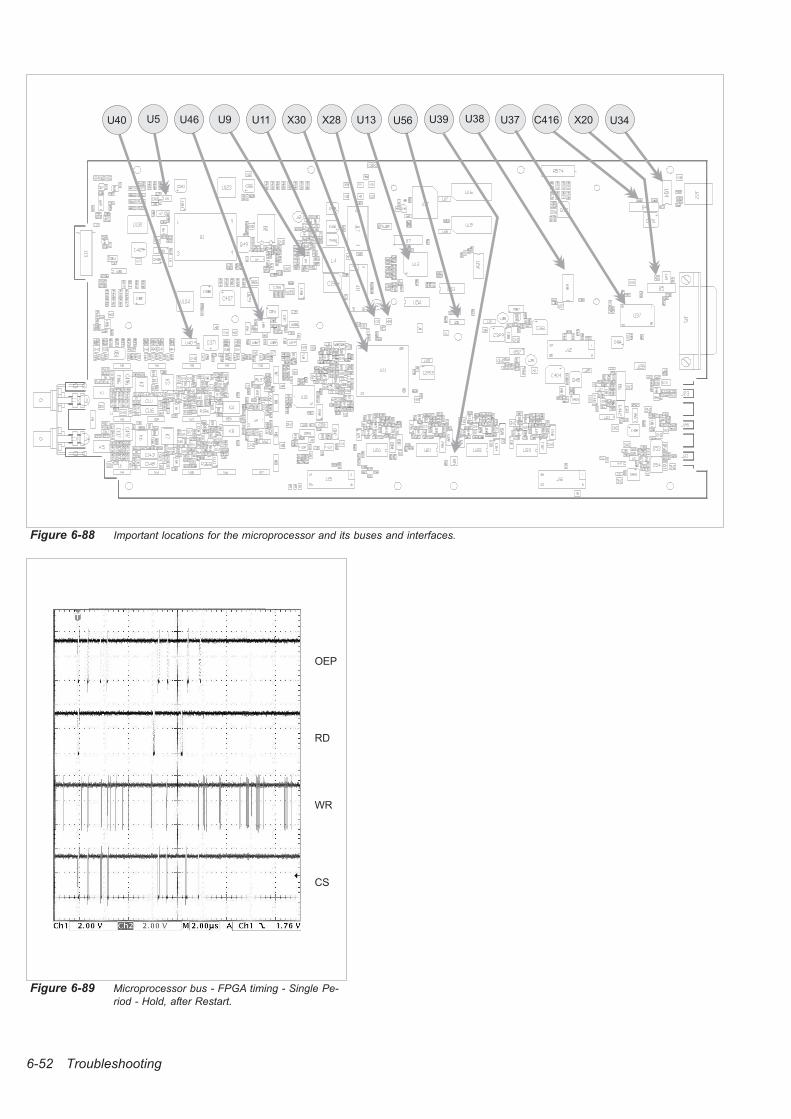
6-52 Troubleshooting
Figure 6-88 Important locations for the microprocessor and its buses and interfaces.
U5 U46 U9U40 X30 X28 U39 U38 U37 C416 X20 U34U11 U56U13
Figure 6-89 Microprocessor bus - FPGA timing - Single Pe-
riod - Hold, after Restart.
CS
WR
RD
OEP
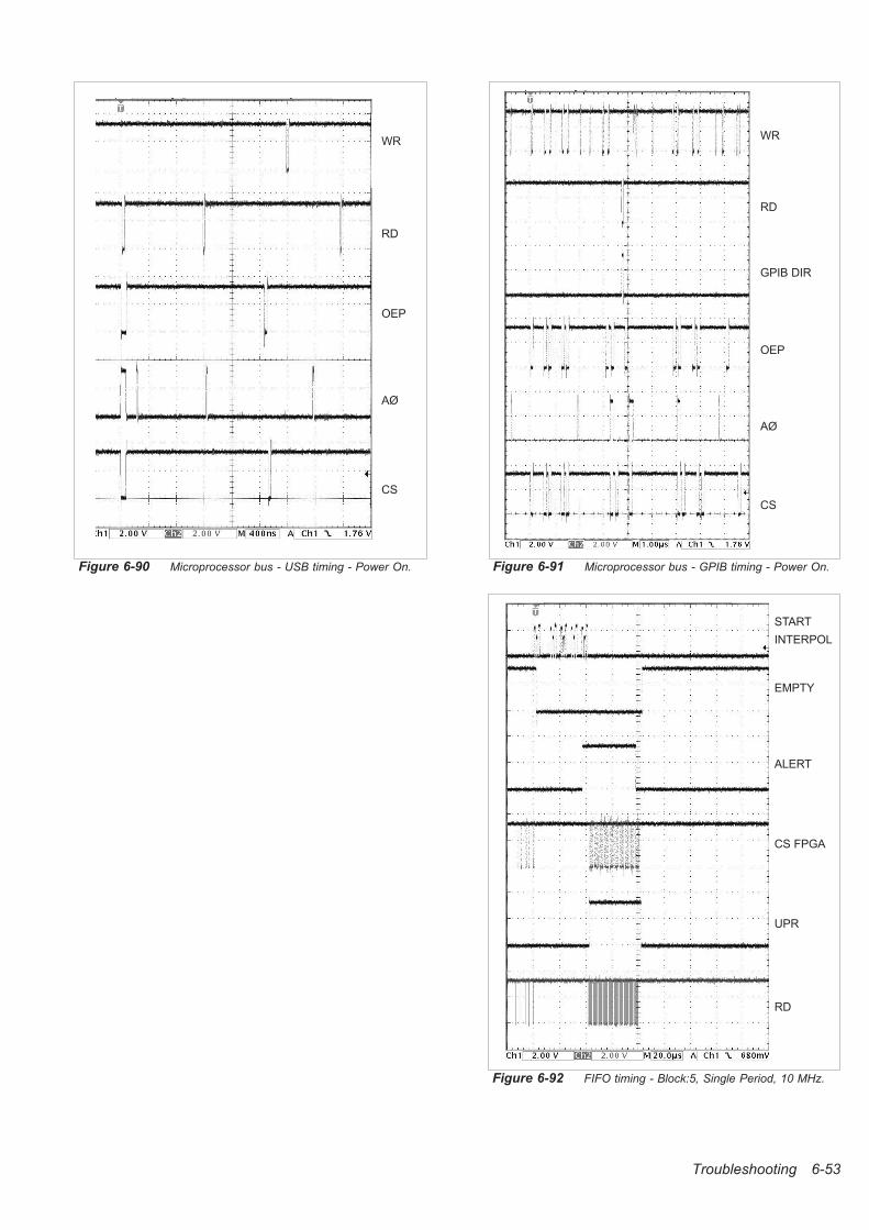
Troubleshooting 6-53
Figure 6-90 Microprocessor bus - USB timing - Power On.
CS
AØ
OEP
RD
WR
Figure 6-91 Microprocessor bus - GPIB timing - Power On.
GPIB DIR
CS
AØ
OEP
RD
WR
Figure 6-92 FIFO timing - Block:5, Single Period, 10 MHz.
EMPTY
UPR
ALERT
START
INTERPOL
CS FPGA
RD
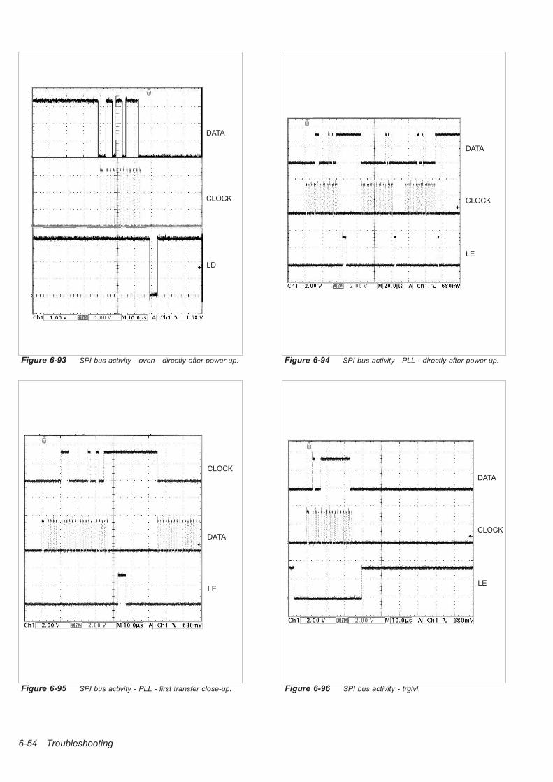
6-54 Troubleshooting
Figure 6-93 SPI bus activity - oven - directly after power-up.
DATA
LD
CLOCK
Figure 6-94 SPI bus activity - PLL - directly after power-up.
DATA
LE
CLOCK
Figure 6-95 SPI bus activity - PLL - first transfer close-up.
DATA
LE
CLOCK
Figure 6-96 SPI bus activity - trglvl.
DATA
LE
CLOCK
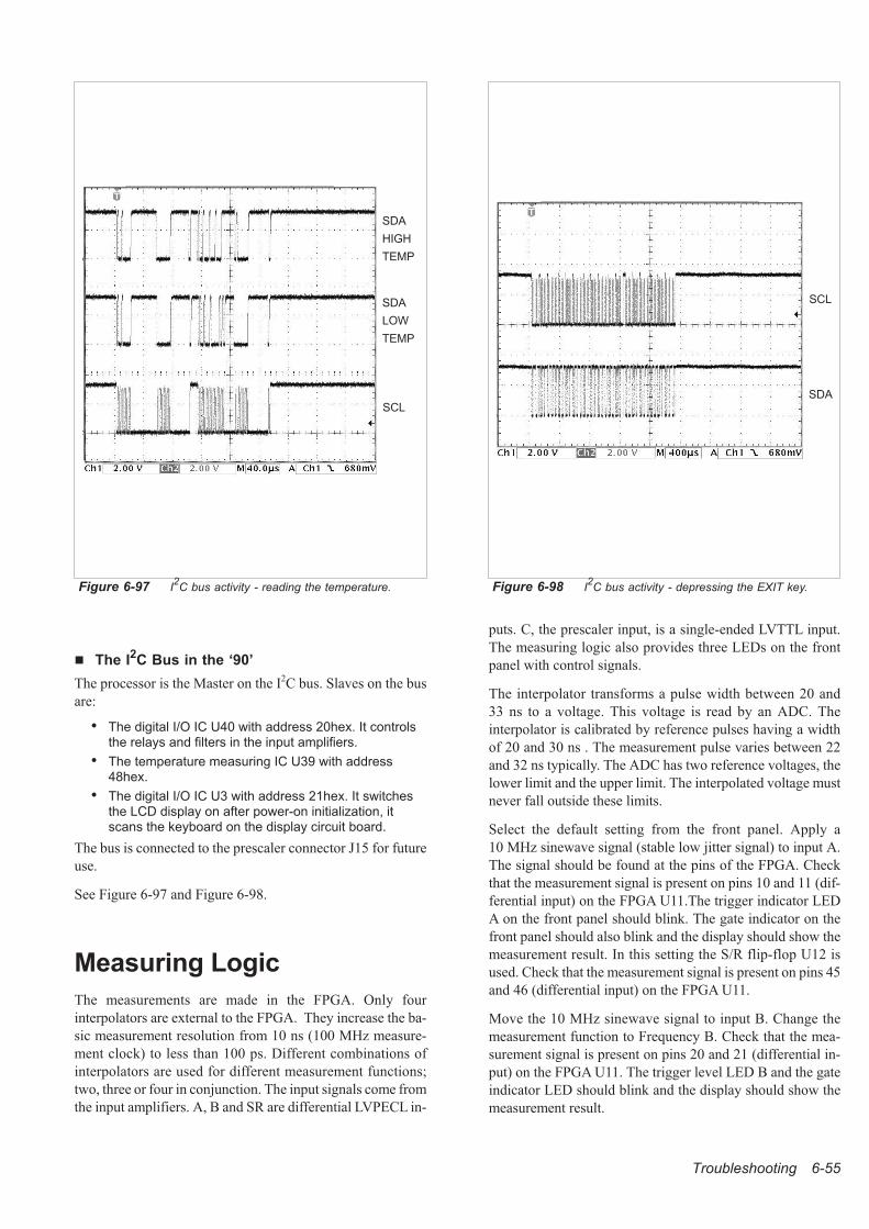
Troubleshooting 6-55
� The I2C Bus in the ‘90’
The processor is the Master on the I2C bus. Slaves on the bus
are:
• The digital I/O IC U40 with address 20hex. It controlsthe relays and filters in the input amplifiers.
• The temperature measuring IC U39 with address48hex.
• The digital I/O IC U3 with address 21hex. It switchesthe LCD display on after power-on initialization, itscans the keyboard on the display circuit board.
The bus is connected to the prescaler connector J15 for future
use.
See Figure 6-97 and Figure 6-98.
Measuring Logic
The measurements are made in the FPGA. Only four
interpolators are external to the FPGA. They increase the ba-
sic measurement resolution from 10 ns (100 MHz measure-
ment clock) to less than 100 ps. Different combinations of
interpolators are used for different measurement functions;
two, three or four in conjunction. The input signals come from
the input amplifiers. A, B and SR are differential LVPECL in-
puts. C, the prescaler input, is a single-ended LVTTL input.
The measuring logic also provides three LEDs on the front
panel with control signals.
The interpolator transforms a pulse width between 20 and
33 ns to a voltage. This voltage is read by an ADC. The
interpolator is calibrated by reference pulses having a width
of 20 and 30 ns . The measurement pulse varies between 22
and 32 ns typically. The ADC has two reference voltages, the
lower limit and the upper limit. The interpolated voltage must
never fall outside these limits.
Select the default setting from the front panel. Apply a
10 MHz sinewave signal (stable low jitter signal) to input A.
The signal should be found at the pins of the FPGA. Check
that the measurement signal is present on pins 10 and 11 (dif-
ferential input) on the FPGA U11.The trigger indicator LED
A on the front panel should blink. The gate indicator on the
front panel should also blink and the display should show the
measurement result. In this setting the S/R flip-flop U12 is
used. Check that the measurement signal is present on pins 45
and 46 (differential input) on the FPGA U11.
Move the 10 MHz sinewave signal to input B. Change the
measurement function to Frequency B. Check that the mea-
surement signal is present on pins 20 and 21 (differential in-
put) on the FPGA U11. The trigger level LED B and the gate
indicator LED should blink and the display should show the
measurement result.
Figure 6-97 I2C bus activity - reading the temperature.
SDA
HIGH
TEMP
SCL
SDA
LOW
TEMP
Figure 6-98 I2C bus activity - depressing the EXIT key.
SCL
SDA
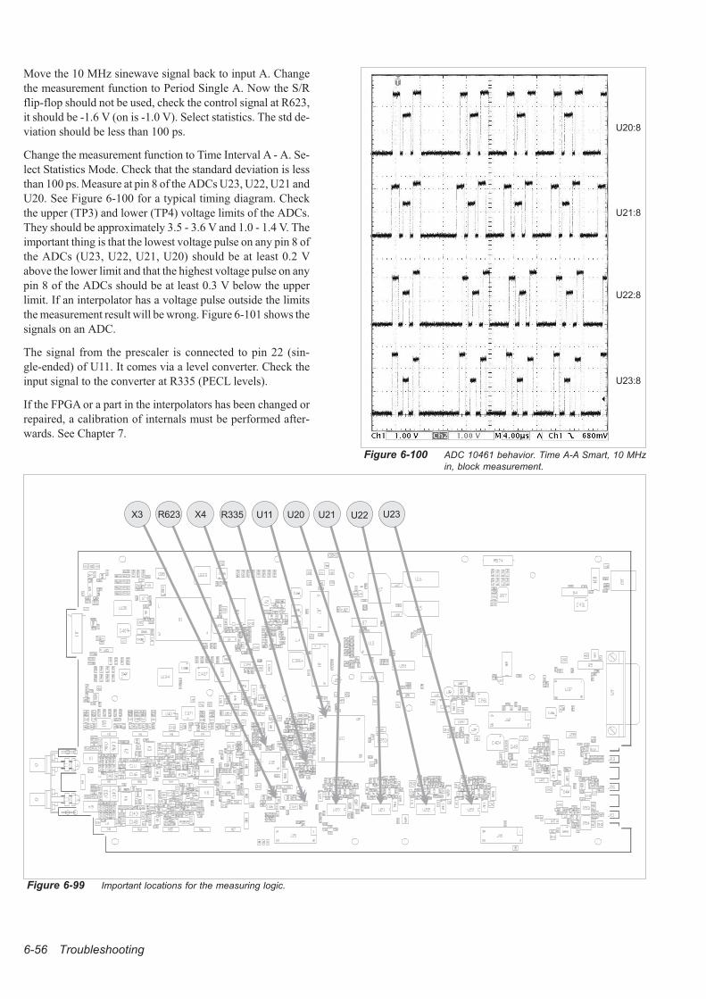
Move the 10 MHz sinewave signal back to input A. Change
the measurement function to Period Single A. Now the S/R
flip-flop should not be used, check the control signal at R623,
it should be -1.6 V (on is -1.0 V). Select statistics. The std de-
viation should be less than 100 ps.
Change the measurement function to Time Interval A - A. Se-
lect Statistics Mode. Check that the standard deviation is less
than 100 ps. Measure at pin 8 of the ADCs U23, U22, U21 and
U20. See Figure 6-100 for a typical timing diagram. Check
the upper (TP3) and lower (TP4) voltage limits of the ADCs.
They should be approximately 3.5 - 3.6 V and 1.0 - 1.4 V. The
important thing is that the lowest voltage pulse on any pin 8 of
the ADCs (U23, U22, U21, U20) should be at least 0.2 V
above the lower limit and that the highest voltage pulse on any
pin 8 of the ADCs should be at least 0.3 V below the upper
limit. If an interpolator has a voltage pulse outside the limits
the measurement result will be wrong. Figure 6-101 shows the
signals on an ADC.
The signal from the prescaler is connected to pin 22 (sin-
gle-ended) of U11. It comes via a level converter. Check the
input signal to the converter at R335 (PECL levels).
If the FPGA or a part in the interpolators has been changed or
repaired, a calibration of internals must be performed after-
wards. See Chapter 7.
6-56 Troubleshooting
Figure 6-99 Important locations for the measuring logic.
R623 X4X3 U11 U20 U21 U23R335 U22
Figure 6-100 ADC 10461 behavior. Time A-A Smart, 10 MHz
in, block measurement.
U21:8
U20:8
U22:8
U23:8
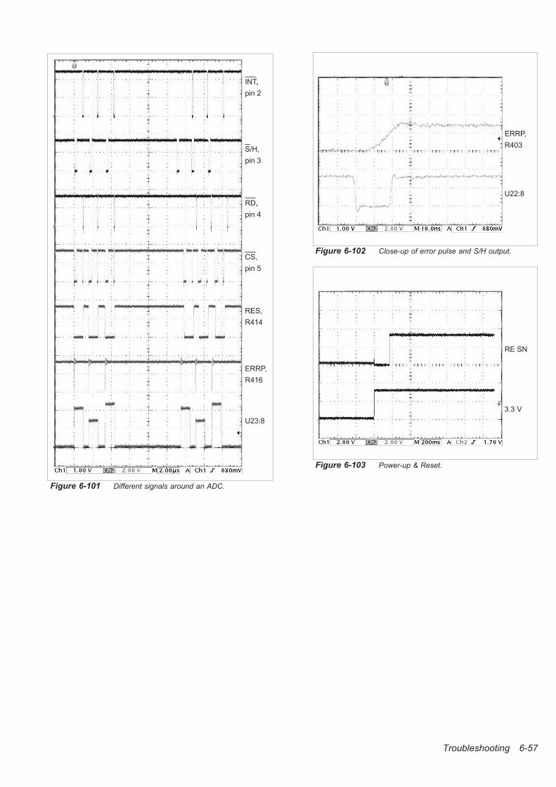
Troubleshooting 6-57
Figure 6-101 Different signals around an ADC.
U23:8
ERRP,
R416
RES,
R414
CS,
pin 5
RD,
pin 4
S/H,
pin 3
INT,
pin 2
Figure 6-102 Close-up of error pulse and S/H output.
U22:8
ERRP,
R403
Figure 6-103 Power-up & Reset.
3.3 V
RE SN
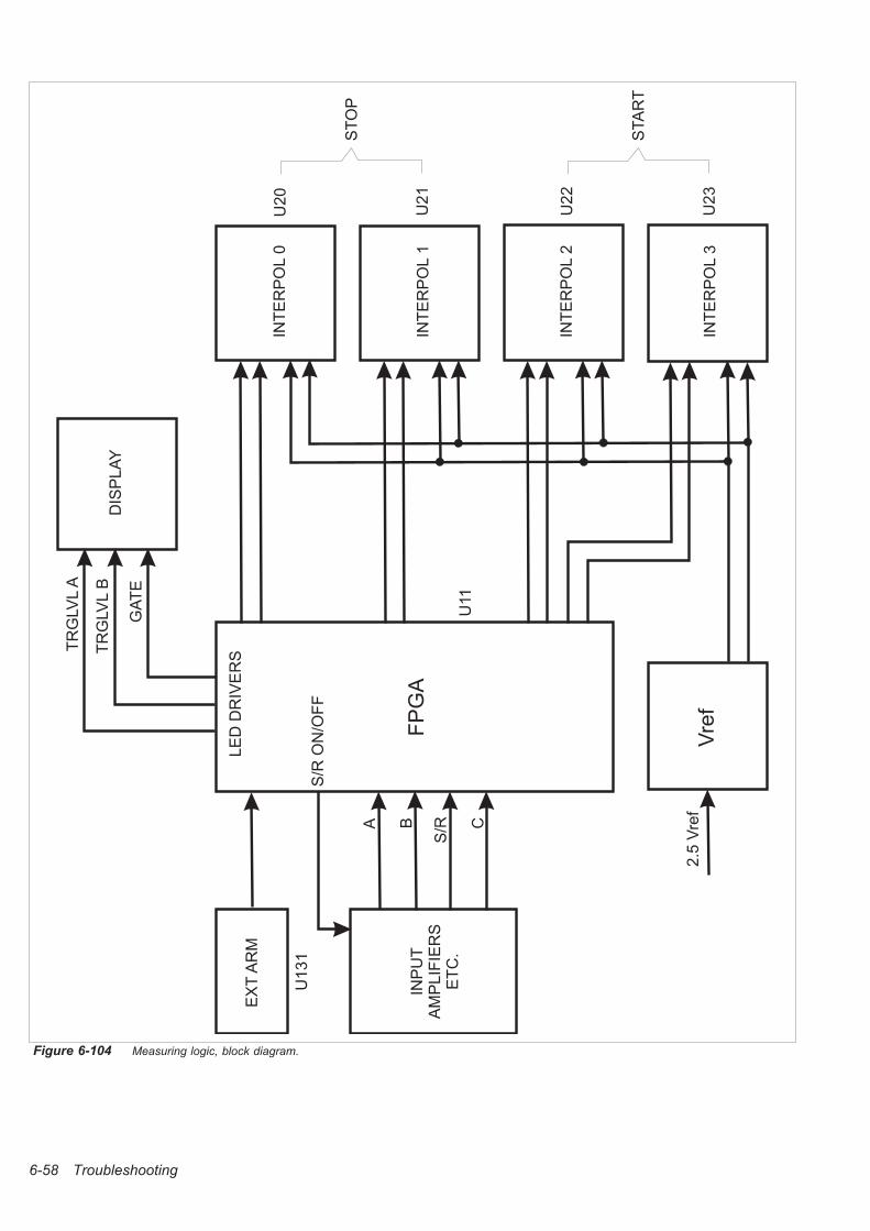
6-58 Troubleshooting
U1
31
S/R
ON
/OF
F
EX
TA
RM
FP
GA
INP
UT
AM
PL
IFIE
RS
ET
C.
A B
S/R C
TR
GLV
LA
TR
GLV
LB
GA
TE
DIS
PL
AY
LE
DD
RIV
ER
S
INT
ER
PO
L0
INT
ER
PO
L1
INT
ER
PO
L2
INT
ER
PO
L3
U2
0
U2
1
U2
2
U2
3
ST
OP
STA
RT
Vre
f2
.5V
ref
U11
Figure 6-104 Measuring logic, block diagram.
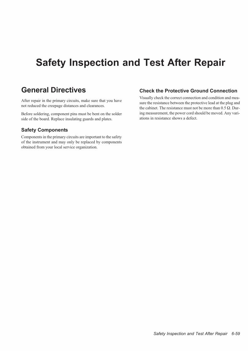
Safety Inspection and Test After Repair
General Directives
After repair in the primary circuits, make sure that you have
not reduced the creepage distances and clearances.
Before soldering, component pins must be bent on the solder
side of the board. Replace insulating guards and plates.
Safety Components
Components in the primary circuits are important to the safety
of the instrument and may only be replaced by components
obtained from your local service organization.
Check the Protective Ground Connection
Visually check the correct connection and condition and mea-
sure the resistance between the protective lead at the plug and
the cabinet. The resistance must not be more than 0.5 �. Dur-
ing measurement, the power cord should be moved. Any vari-
ations in resistance shows a defect.
Safety Inspection and Test After Repair 6-59

This page is intentionally left blank.
6-60 Safety Inspection and Test After Repair
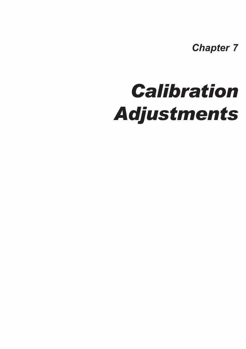
Chapter 7
Calibration
Adjustments
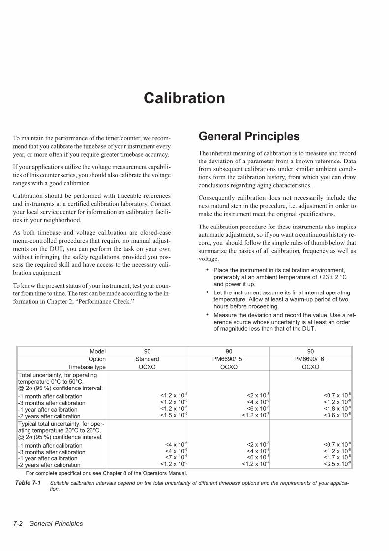
Calibration
To maintain the performance of the timer/counter, we recom-
mend that you calibrate the timebase of your instrument every
year, or more often if you require greater timebase accuracy.
If your applications utilize the voltage measurement capabili-
ties of this counter series, you should also calibrate the voltage
ranges with a good calibrator.
Calibration should be performed with traceable references
and instruments at a certified calibration laboratory. Contact
your local service center for information on calibration facili-
ties in your neighborhood.
As both timebase and voltage calibration are closed-case
menu-controlled procedures that require no manual adjust-
ments on the DUT, you can perform the task on your own
without infringing the safety regulations, provided you pos-
sess the required skill and have access to the necessary cali-
bration equipment.
To know the present status of your instrument, test your coun-
ter from time to time. The test can be made according to the in-
formation in Chapter 2, “Performance Check.”
General Principles
The inherent meaning of calibration is to measure and record
the deviation of a parameter from a known reference. Data
from subsequent calibrations under similar ambient condi-
tions form the calibration history, from which you can draw
conclusions regarding aging characteristics.
Consequently calibration does not necessarily include the
next natural step in the procedure, i.e. adjustment in order to
make the instrument meet the original specifications.
The calibration procedure for these instruments also implies
automatic adjustment, so if you want a continuous history re-
cord, you should follow the simple rules of thumb below that
summarize the basics of all calibration, frequency as well as
voltage.
• Place the instrument in its calibration environment,preferably at an ambient temperature of +23 ± 2 °Cand power it up.
• Let the instrument assume its final internal operatingtemperature. Allow at least a warm-up period of twohours before proceeding.
• Measure the deviation and record the value. Use a ref-erence source whose uncertainty is at least an orderof magnitude less than that of the DUT.
7-2 General Principles
Model 90 90 90
Option Standard PM6690/_5_ PM6690/_6_
Timebase type UCXO OCXO OCXO
Total uncertainty, for operatingtemperature 0°C to 50°C,@ 2 (95 %) confidence interval:
-1 month after calibration-3 months after calibration-1 year after calibration-2 years after calibration
<1.2 x 10⁻⁵
<1.2 x 10⁻⁵
<1.2 x 10⁻⁵
<1.5 x 10⁻⁵
<2 x 10⁻⁸
<4 x 10⁻⁸
<6 x 10⁻⁸
<1.2 x 10⁻⁷
<0.7 x 10⁻⁸
<1.2 x 10⁻⁸
<1.8 x 10⁻⁸
<3.6 x 10⁻⁸
Typical total uncertainty, for oper-ating temperature 20°C to 26°C,@ 2 (95 %) confidence interval:
-1 month after calibration-3 months after calibration-1 year after calibration-2 years after calibration
<4 x 10⁻⁶
<4 x 10⁻⁶
<7 x 10⁻⁶
<1.2 x 10⁻⁵
<2 x 10⁻⁸
<4 x 10⁻⁸
<6 x 10⁻⁸
<1.2 x 10⁻⁷
<0.7 x 10⁻⁸
<1.2 x 10⁻⁸
<1.7 x 10⁻⁸
<3.5 x 10⁻⁸
For complete specifications see Chapter 8 of the Operators Manual.
Table 7-1 Suitable calibration intervals depend on the total uncertainty of different timebase options and the requirements of your applica-
tion.
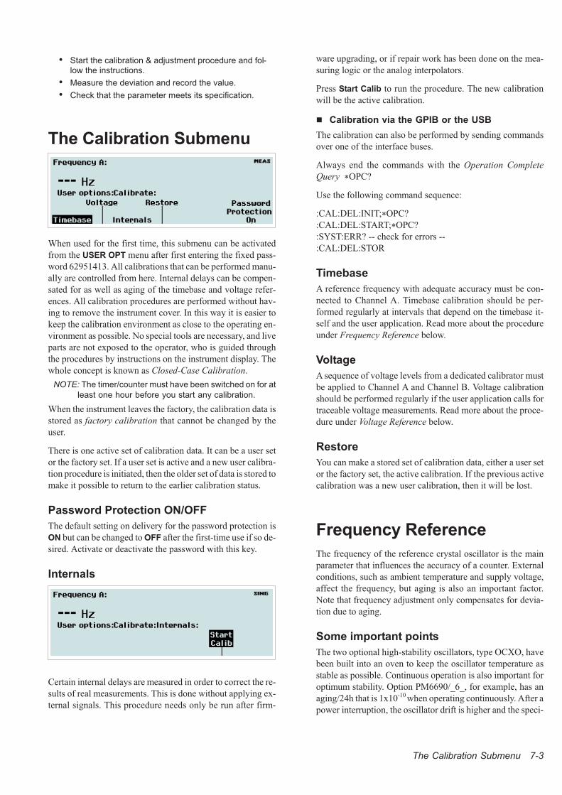
• Start the calibration & adjustment procedure and fol-low the instructions.
• Measure the deviation and record the value.
• Check that the parameter meets its specification.
The Calibration Submenu
When used for the first time, this submenu can be activated
from the USER OPT menu after first entering the fixed pass-
word 62951413. All calibrations that can be performed manu-
ally are controlled from here. Internal delays can be compen-
sated for as well as aging of the timebase and voltage refer-
ences. All calibration procedures are performed without hav-
ing to remove the instrument cover. In this way it is easier to
keep the calibration environment as close to the operating en-
vironment as possible. No special tools are necessary, and live
parts are not exposed to the operator, who is guided through
the procedures by instructions on the instrument display. The
whole concept is known as Closed-Case Calibration.
NOTE: The timer/counter must have been switched on for at
least one hour before you start any calibration.
When the instrument leaves the factory, the calibration data is
stored as factory calibration that cannot be changed by the
user.
There is one active set of calibration data. It can be a user set
or the factory set. If a user set is active and a new user calibra-
tion procedure is initiated, then the older set of data is stored to
make it possible to return to the earlier calibration status.
Password Protection ON/OFF
The default setting on delivery for the password protection is
ON but can be changed to OFF after the first-time use if so de-
sired. Activate or deactivate the password with this key.
Internals
Certain internal delays are measured in order to correct the re-
sults of real measurements. This is done without applying ex-
ternal signals. This procedure needs only be run after firm-
ware upgrading, or if repair work has been done on the mea-
suring logic or the analog interpolators.
Press Start Calib to run the procedure. The new calibration
will be the active calibration.
� Calibration via the GPIB or the USB
The calibration can also be performed by sending commands
over one of the interface buses.
Always end the commands with the Operation Complete
Query *OPC?
Use the following command sequence:
:CAL:DEL:INIT;*OPC?
:CAL:DEL:START;*OPC?
:SYST:ERR? -- check for errors --
:CAL:DEL:STOR
Timebase
A reference frequency with adequate accuracy must be con-
nected to Channel A. Timebase calibration should be per-
formed regularly at intervals that depend on the timebase it-
self and the user application. Read more about the procedure
under Frequency Reference below.
Voltage
A sequence of voltage levels from a dedicated calibrator must
be applied to Channel A and Channel B. Voltage calibration
should be performed regularly if the user application calls for
traceable voltage measurements. Read more about the proce-
dure under Voltage Reference below.
Restore
You can make a stored set of calibration data, either a user set
or the factory set, the active calibration. If the previous active
calibration was a new user calibration, then it will be lost.
Frequency Reference
The frequency of the reference crystal oscillator is the main
parameter that influences the accuracy of a counter. External
conditions, such as ambient temperature and supply voltage,
affect the frequency, but aging is also an important factor.
Note that frequency adjustment only compensates for devia-
tion due to aging.
Some important points
The two optional high-stability oscillators, type OCXO, have
been built into an oven to keep the oscillator temperature as
stable as possible. Continuous operation is also important for
optimum stability. Option PM6690/_6_, for example, has an
aging/24h that is 1x10⁻¹⁰ when operating continuously. After a
power interruption, the oscillator drift is higher and the speci-
The Calibration Submenu 7-3
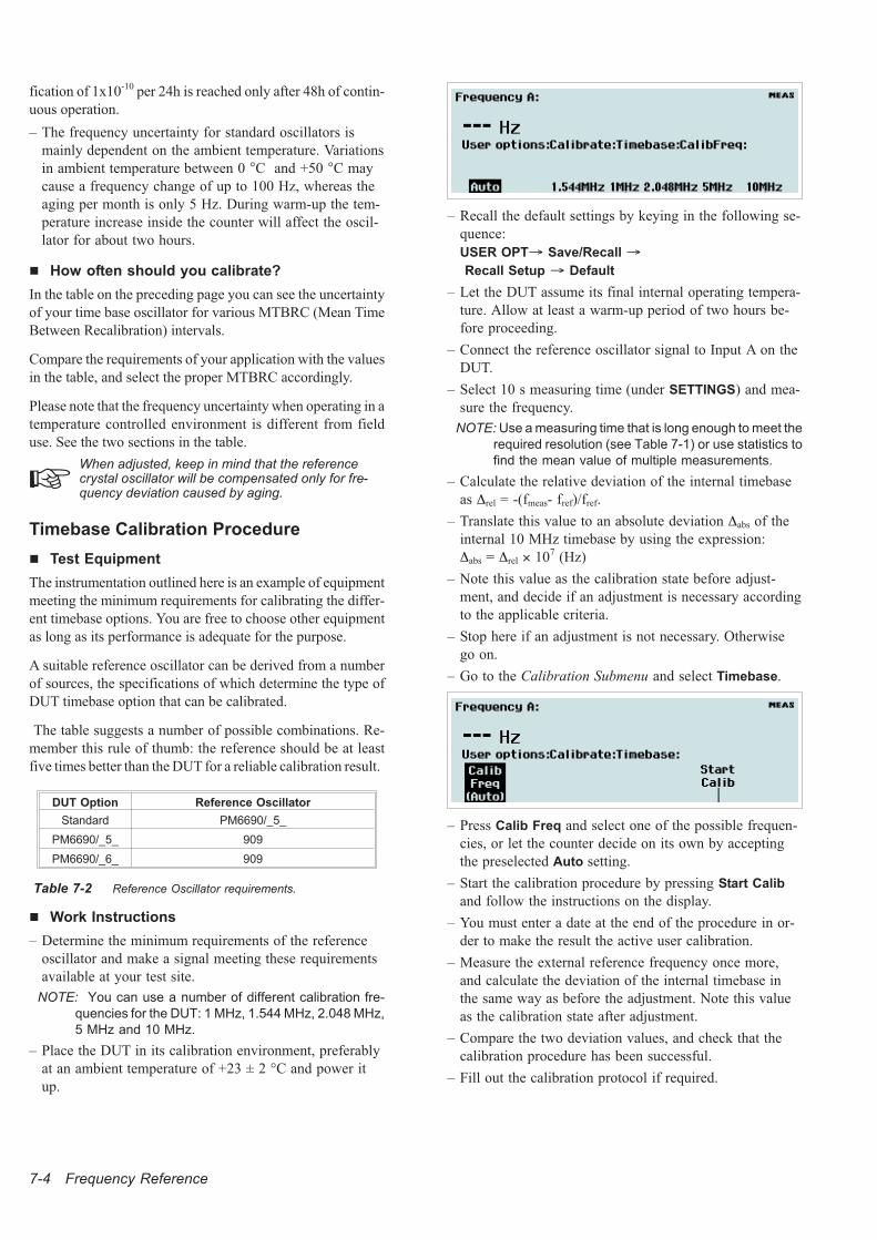
fication of 1x10⁻¹⁰ per 24h is reached only after 48h of contin-
uous operation.
– The frequency uncertainty for standard oscillators is
mainly dependent on the ambient temperature. Variations
in ambient temperature between 0 �C and +50 �C may
cause a frequency change of up to 100 Hz, whereas the
aging per month is only 5 Hz. During warm-up the tem-
perature increase inside the counter will affect the oscil-
lator for about two hours.
� How often should you calibrate?
In the table on the preceding page you can see the uncertainty
of your time base oscillator for various MTBRC (Mean Time
Between Recalibration) intervals.
Compare the requirements of your application with the values
in the table, and select the proper MTBRC accordingly.
Please note that the frequency uncertainty when operating in a
temperature controlled environment is different from field
use. See the two sections in the table.
�When adjusted, keep in mind that the referencecrystal oscillator will be compensated only for fre-quency deviation caused by aging.
Timebase Calibration Procedure
� Test Equipment
The instrumentation outlined here is an example of equipment
meeting the minimum requirements for calibrating the differ-
ent timebase options. You are free to choose other equipment
as long as its performance is adequate for the purpose.
A suitable reference oscillator can be derived from a number
of sources, the specifications of which determine the type of
DUT timebase option that can be calibrated.
The table suggests a number of possible combinations. Re-
member this rule of thumb: the reference should be at least
five times better than the DUT for a reliable calibration result.
� Work Instructions
– Determine the minimum requirements of the reference
oscillator and make a signal meeting these requirements
available at your test site.
NOTE: You can use a number of different calibration fre-
quencies for the DUT: 1 MHz, 1.544 MHz, 2.048 MHz,
5 MHz and 10 MHz.
– Place the DUT in its calibration environment, preferably
at an ambient temperature of +23 ± 2 °C and power it
up.
– Recall the default settings by keying in the following se-
quence:
USER OPT� Save/Recall �
Recall Setup � Default
– Let the DUT assume its final internal operating tempera-
ture. Allow at least a warm-up period of two hours be-
fore proceeding.
– Connect the reference oscillator signal to Input A on the
DUT.
– Select 10 s measuring time (under SETTINGS) and mea-
sure the frequency.
NOTE: Use a measuring time that is long enough to meet the
required resolution (see Table 7-1) or use statistics to
find the mean value of multiple measurements.
– Calculate the relative deviation of the internal timebase
as �rel = -(fmeas- fref)/fref.
– Translate this value to an absolute deviation �abs of the
internal 10 MHz timebase by using the expression:
�abs = �rel � 107 (Hz)
– Note this value as the calibration state before adjust-
ment, and decide if an adjustment is necessary according
to the applicable criteria.
– Stop here if an adjustment is not necessary. Otherwise
go on.
– Go to the Calibration Submenu and select Timebase.
– Press Calib Freq and select one of the possible frequen-
cies, or let the counter decide on its own by accepting
the preselected Auto setting.
– Start the calibration procedure by pressing Start Calib
and follow the instructions on the display.
– You must enter a date at the end of the procedure in or-
der to make the result the active user calibration.
– Measure the external reference frequency once more,
and calculate the deviation of the internal timebase in
the same way as before the adjustment. Note this value
as the calibration state after adjustment.
– Compare the two deviation values, and check that the
calibration procedure has been successful.
– Fill out the calibration protocol if required.
7-4 Frequency Reference
DUT Option Reference Oscillator
Standard PM6690/_5_
PM6690/_5_ 909
PM6690/_6_ 909
Table 7-2 Reference Oscillator requirements.
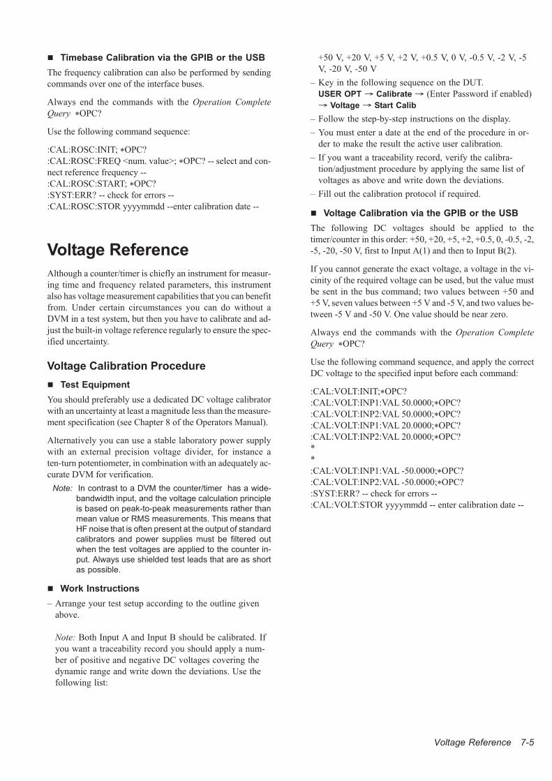
Voltage Reference 7-5
� Timebase Calibration via the GPIB or the USB
The frequency calibration can also be performed by sending
commands over one of the interface buses.
Always end the commands with the Operation Complete
Query *OPC?
Use the following command sequence:
:CAL:ROSC:INIT; *OPC?
:CAL:ROSC:FREQ <num. value>; *OPC? -- select and con-
nect reference frequency --
:CAL:ROSC:START; *OPC?
:SYST:ERR? -- check for errors --
:CAL:ROSC:STOR yyyymmdd --enter calibration date --
Voltage Reference
Although a counter/timer is chiefly an instrument for measur-
ing time and frequency related parameters, this instrument
also has voltage measurement capabilities that you can benefit
from. Under certain circumstances you can do without a
DVM in a test system, but then you have to calibrate and ad-
just the built-in voltage reference regularly to ensure the spec-
ified uncertainty.
Voltage Calibration Procedure
� Test Equipment
You should preferably use a dedicated DC voltage calibrator
with an uncertainty at least a magnitude less than the measure-
ment specification (see Chapter 8 of the Operators Manual).
Alternatively you can use a stable laboratory power supply
with an external precision voltage divider, for instance a
ten-turn potentiometer, in combination with an adequately ac-
curate DVM for verification.
Note: In contrast to a DVM the counter/timer has a wide-
bandwidth input, and the voltage calculation principle
is based on peak-to-peak measurements rather than
mean value or RMS measurements. This means that
HF noise that is often present at the output of standard
calibrators and power supplies must be filtered out
when the test voltages are applied to the counter in-
put. Always use shielded test leads that are as short
as possible.
� Work Instructions
– Arrange your test setup according to the outline given
above.
Note: Both Input A and Input B should be calibrated. If
you want a traceability record you should apply a num-
ber of positive and negative DC voltages covering the
dynamic range and write down the deviations. Use the
following list:
+50 V, +20 V, +5 V, +2 V, +0.5 V, 0 V, -0.5 V, -2 V, -5
V, -20 V, -50 V
– Key in the following sequence on the DUT.
USER OPT � Calibrate � (Enter Password if enabled)
� Voltage � Start Calib
– Follow the step-by-step instructions on the display.
– You must enter a date at the end of the procedure in or-
der to make the result the active user calibration.
– If you want a traceability record, verify the calibra-
tion/adjustment procedure by applying the same list of
voltages as above and write down the deviations.
– Fill out the calibration protocol if required.
� Voltage Calibration via the GPIB or the USB
The following DC voltages should be applied to the
timer/counter in this order: +50, +20, +5, +2, +0.5, 0, -0.5, -2,
-5, -20, -50 V, first to Input A(1) and then to Input B(2).
If you cannot generate the exact voltage, a voltage in the vi-
cinity of the required voltage can be used, but the value must
be sent in the bus command; two values between +50 and
+5 V, seven values between +5 V and -5 V, and two values be-
tween -5 V and -50 V. One value should be near zero.
Always end the commands with the Operation Complete
Query *OPC?
Use the following command sequence, and apply the correct
DC voltage to the specified input before each command:
:CAL:VOLT:INIT;*OPC?
:CAL:VOLT:INP1:VAL 50.0000;*OPC?
:CAL:VOLT:INP2:VAL 50.0000;*OPC?
:CAL:VOLT:INP1:VAL 20.0000;*OPC?
:CAL:VOLT:INP2:VAL 20.0000;*OPC?
*
*
:CAL:VOLT:INP1:VAL -50.0000;*OPC?
:CAL:VOLT:INP2:VAL -50.0000;*OPC?
:SYST:ERR? -- check for errors --
:CAL:VOLT:STOR yyyymmdd -- enter calibration date --
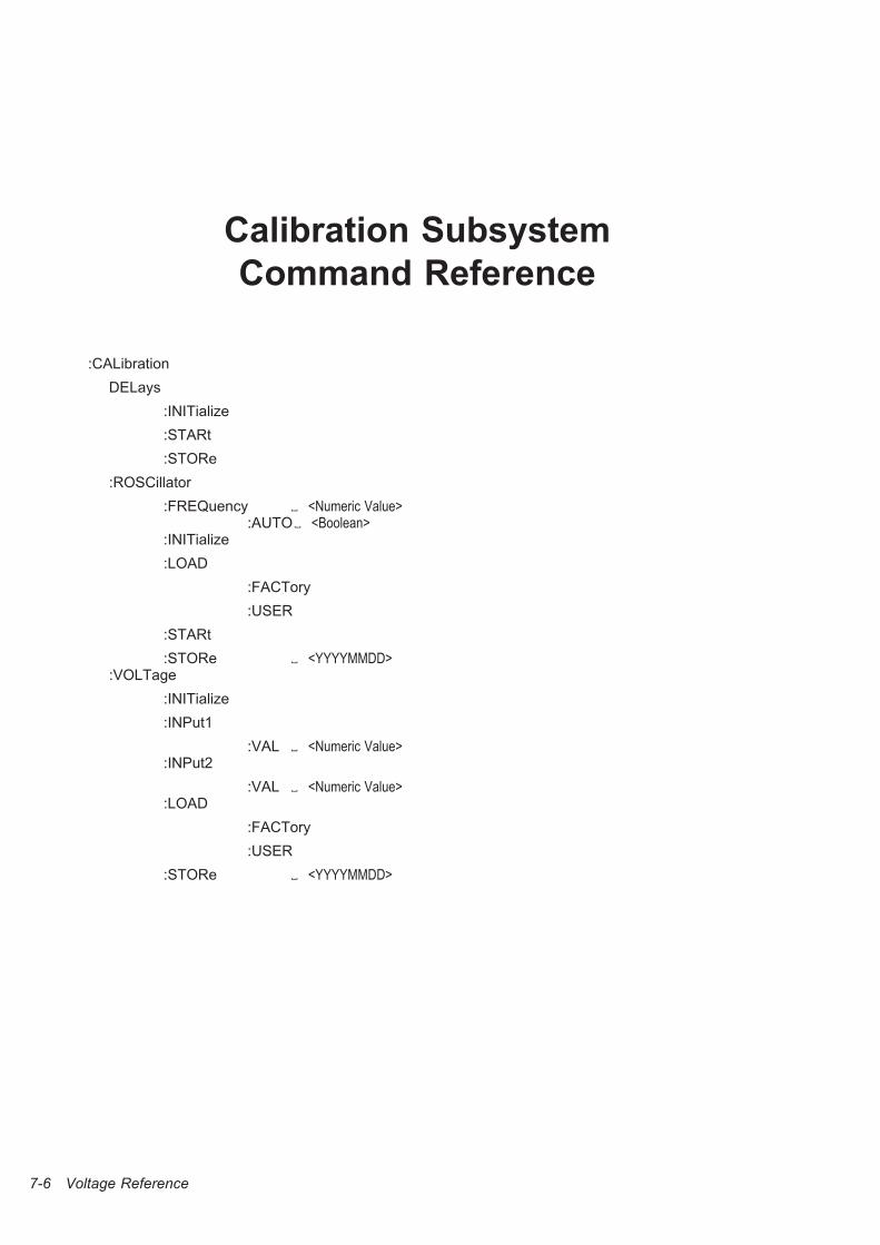
7-6 Voltage Reference
Calibration Subsystem
Command Reference
:CALibration
DELays
:INITialize
:STARt
:STORe
:ROSCillator
:FREQuency � <Numeric Value>
:AUTO � <Boolean>
:INITialize
:LOAD
:FACTory
:USER
:STARt
:STORe � <YYYYMMDD>
:VOLTage
:INITialize
:INPut1
:VAL � <Numeric Value>
:INPut2
:VAL � <Numeric Value>
:LOAD
:FACTory
:USER
:STORe � <YYYYMMDD>
Voltage Reference 7-7
:CALibration :DELays :INITialize
Calibration of Internal Delays
Initializes the calibration process.
:CALibration :DELays :STARt
Calibration of Internal Delays
Starts the calibration process.
:CALibration :DELays :STORe
Calibration of Internal Delays
Ends the calibration process and stores the calibration factors.
:CALibration :ROSCillator :FREQuency�<Numeric value>
Calibration of Reference Oscillator
Selects the reference frequency used for the timebase calibration. AUTO is automatically set to OFF.
Parameters:
<Numeric value> = (1E+6 | 1.544E+6 |2.048E+6 | 5E+6 | 10E+6)
Returned format: <Numeric value>
*RST condition: Not affecting this setting
7-8 Voltage Reference
:CALibration :ROSCillator :FREQuency :AUTO�<Boolean>
Calibration of Reference Oscillator
Switches the AUTO mode ON/OFF for the reference frequency calibration. If ON, the timer/counter measures theapplied reference frequency before the start of the calibration process and adjusts the calculation algorithm ac-cordingly.
Parameters:
<Boolean> = (1 | ON / 0 | OFF)
Returned format: 1 | 0
*RST condition: Not affecting this setting
:CALibration :ROSCillator :INITialize
Calibration of Reference OscillatorInitializes the calibration process.
:CALibration :ROSCillator :LOAD :FACTory
Restore Factory Calibration
Recalls the calibration factors stored by the factory before delivery or after service.
:CALibration :ROSCillator :LOAD :USER
Restore User Calibration
Recalls the calibration factors last stored by the user.
Voltage Reference 7-9
:CALibration :ROSCillator :STARt
Start Calibration
Starts the calibration process after an external reference source has been connected to Input A.
:CALibration :ROSCillator :STORe�<YYYYMMDD>
Store User Calibration
Ends the calibration process and stores the calibration factors using the date code YYYYMMDD, that is year(4 digits), month (2 digits), and day (2 digits).
Example:SEND� :CAL:ROSC:STOR 20040731
:CALibration :VOLTage :INITialize
Calibration of Reference Voltage
Initializes the voltage calibration process.
:CALibration :VOLTage :INPut«[1]|2» :VAL�<Numeric Value>
DC Voltage Calibration
Calibrates a DC voltage within the range -50 V - +50 V if the corresponding voltage from a voltage referencesource is applied to the input that is addressed in the command.
Example for Input A (1):SEND� :CAL:VOLT:INP:VAL 5
+5 V is applied to input A before sending the command.
Example for Input B (2):SEND� CAL:VOLT:INP2:VAL -20
-20 V is applied to input B before sending the command.
Note: The DC voltages must be sent in a prescribed order. See page 7-5.
7-10 Voltage Reference
:CALibration :VOLTage :LOAD :FACTory
Restore Factory Calibration
Recalls the calibration factors stored by the factory before delivery or after service.
:CALibration :VOLTage :LOAD :USER
Restore User Calibration
Recalls the calibration factors last stored by the user.
:CALibration :VOLTage :STORe�<YYYYMMDD>
Store User Calibration
Ends the calibration process and stores the calibration factors using the date code YYYYMMDD, that is year (4digits), month (2 digits), and day (2 digits).
Example:SEND� :CAL:VOLT:STOR 20040731
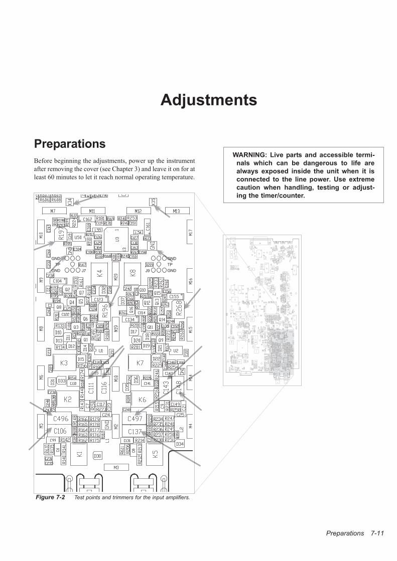
Adjustments
Preparations
Before beginning the adjustments, power up the instrument
after removing the cover (see Chapter 3) and leave it on for at
least 60 minutes to let it reach normal operating temperature.
WARNING: Live parts and accessible termi-
nals which can be dangerous to life are
always exposed inside the unit when it is
connected to the line power. Use extreme
caution when handling, testing or adjust-
ing the timer/counter.
Preparations 7-11
Figure 7-2 Test points and trimmers for the input amplifiers.
GND
TP
GND
GND
TP
GND J9J7
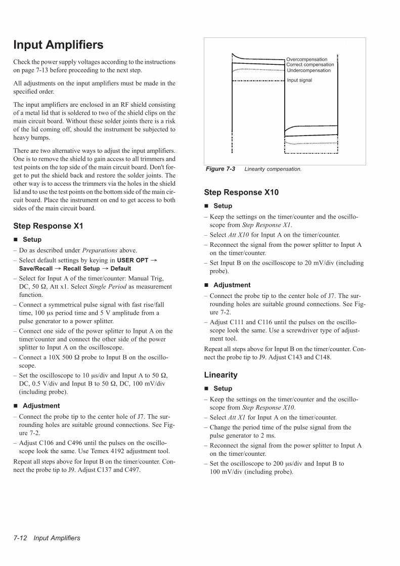
Input Amplifiers
Check the power supply voltages according to the instructions
on page 7-13 before proceeding to the next step.
All adjustments on the input amplifiers must be made in the
specified order.
The input amplifiers are enclosed in an RF shield consisting
of a metal lid that is soldered to two of the shield clips on the
main circuit board. Without these solder joints there is a risk
of the lid coming off, should the instrument be subjected to
heavy bumps.
There are two alternative ways to adjust the input amplifiers.
One is to remove the shield to gain access to all trimmers and
test points on the top side of the main circuit board. Don't for-
get to put the shield back and restore the solder joints. The
other way is to access the trimmers via the holes in the shield
lid and to use the test points on the bottom side of the main cir-
cuit board. Place the instrument on end to get access to both
sides of the main circuit board.
Step Response X1
� Setup
– Do as described under Preparations above.
– Select default settings by keying in USER OPT �
Save/Recall � Recall Setup � Default
– Select for Input A of the timer/counter: Manual Trig,
DC, 50 �, Att x1. Select Single Period as measurement
function.
– Connect a symmetrical pulse signal with fast rise/fall
time, 100 �s period time and 5 V amplitude from a
pulse generator to a power splitter.
– Connect one side of the power splitter to Input A on the
timer/counter and connect the other side of the power
splitter to Input A on the oscilloscope.
– Connect a 10X 500 � probe to Input B on the oscillo-
scope.
– Set the oscilloscope to 10 �s/div and Input A to 50 �,
DC, 0.5 V/div and Input B to 50 �, DC, 100 mV/div
(including probe).
� Adjustment
– Connect the probe tip to the center hole of J7. The sur-
rounding holes are suitable ground connections. See Fig-
ure 7-2.
– Adjust C106 and C496 until the pulses on the oscillo-
scope look the same. Use Temex 4192 adjustment tool.
Repeat all steps above for Input B on the timer/counter. Con-
nect the probe tip to J9. Adjust C137 and C497.
Step Response X10
� Setup
– Keep the settings on the timer/counter and the oscillo-
scope from Step Response X1.
– Select Att X10 for Input A on the timer/counter.
– Reconnect the signal from the power splitter to Input A
on the timer/counter.
– Set Input B on the oscilloscope to 20 mV/div (including
probe).
� Adjustment
– Connect the probe tip to the center hole of J7. The sur-
rounding holes are suitable ground connections. See Fig-
ure 7-2.
– Adjust C111 and C116 until the pulses on the oscillo-
scope look the same. Use a screwdriver type of adjust-
ment tool.
Repeat all steps above for Input B on the timer/counter. Con-
nect the probe tip to J9. Adjust C143 and C148.
Linearity
� Setup
– Keep the settings on the timer/counter and the oscillo-
scope from Step Response X10.
– Select Att X1 for Input A on the timer/counter.
– Change the period time of the pulse signal from the
pulse generator to 2 ms.
– Reconnect the signal from the power splitter to Input A
on the timer/counter.
– Set the oscilloscope to 200 �s/div and Input B to
100 mV/div (including probe).
7-12 Input Amplifiers
Overcompensation
Undercompensation
Correct compensation
Input signal
Figure 7-3 Linearity compensation.
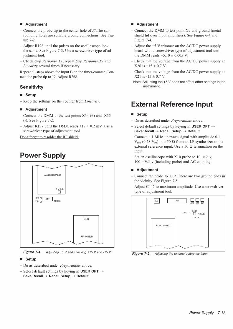
� Adjustment
– Connect the probe tip to the center hole of J7.The sur-
rounding holes are suitable ground connections. See Fig-
ure 7-2.
– Adjust R196 until the pulses on the oscilloscope look
the same. See Figure 7-3. Use a screwdriver type of ad-
justment tool.
– Check Step Response X1, repeat Step Response X1 and
Linearity several times if necessary.
Repeat all steps above for Input B on the timer/counter. Con-
nect the probe tip to J9. Adjust R268.
Sensitivity
� Setup
– Keep the settings on the counter from Linearity.
� Adjustment
– Connect the DMM to the test points X34 (+) and X35
(-). See Figure 7-2.
– Adjust R197 until the DMM reads +17 ± 0.2 mV. Use a
screwdriver type of adjustment tool.
Don't forget to resolder the RF shield.
Power Supply
� Setup
– Do as described under Preparations above.
– Select default settings by keying in USER OPT �
Save/Recall � Recall Setup � Default
� Adjustment
– Connect the DMM to test point X9 and ground (metal
shield lid over input amplifiers). See Figure 6-4 and
Figure 7-4.
– Adjust the +5 V trimmer on the AC/DC power supply
board with a screwdriver type of adjustment tool until
the DMM reads +5.10 ± 0.005 V.
– Check that the voltage from the AC/DC power supply at
X26 is +15 ± 0.7 V.
– Check that the voltage from the AC/DC power supply at
X21 is -15 ± 0.7 V.
Note: Adjusting the +5 V does not affect other settings in the
instrument.
External Reference Input
� Setup
– Do as described under Preparations above.
– Select default settings by keying in USER OPT �
Save/Recall � Recall Setup � Default
– Connect a 1 MHz sinewave signal with amplitude 0.1
Vrms (0.28 Vpp) into 50 � from an LF synthesizer to the
external reference input. Use a 50 � termination on the
input.
– Set an oscilloscope with X10 probe to 10 �s/div,
100 mV/div (including probe) and AC coupling.
� Adjustment
– Connect the probe to X19. There are two ground pads in
the vicinity. See Figure 7-5.
– Adjust C442 to maximum amplitude. Use a screwdriver
type of adjustment tool.
Power Supply 7-13
+5 V adj.
J17X26
X9
X21
GND
AC/DC BOARD
RF SHIELD
Figure 7-4 Adjusting +5 V and checking +15 V and -15 V.
C442
X19
GNDGND
AC/DC BOARD
J22 J25J23 J26 J21
Figure 7-5 Adjusting the external reference input.
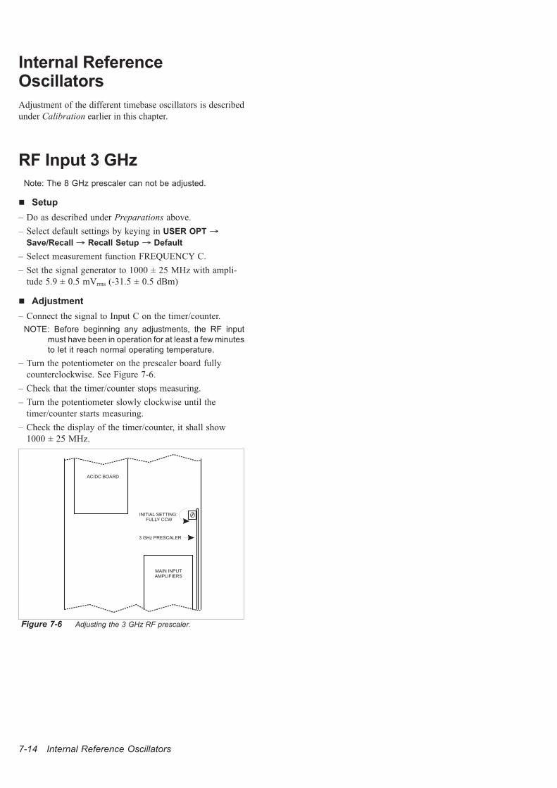
Internal ReferenceOscillators
Adjustment of the different timebase oscillators is described
under Calibration earlier in this chapter.
RF Input 3 GHz
Note: The 8 GHz prescaler can not be adjusted.
� Setup
– Do as described under Preparations above.
– Select default settings by keying in USER OPT �
Save/Recall � Recall Setup � Default
– Select measurement function FREQUENCY C.
– Set the signal generator to 1000 ± 25 MHz with ampli-
tude 5.9 ± 0.5 mVrms (-31.5 ± 0.5 dBm)
� Adjustment
– Connect the signal to Input C on the timer/counter.
NOTE: Before beginning any adjustments, the RF input
must have been in operation for at least a few minutes
to let it reach normal operating temperature.
– Turn the potentiometer on the prescaler board fully
counterclockwise. See Figure 7-6.
– Check that the timer/counter stops measuring.
– Turn the potentiometer slowly clockwise until the
timer/counter starts measuring.
– Check the display of the timer/counter, it shall show
1000 ± 25 MHz.
7-14 Internal Reference Oscillators
AC/DC BOARD
MAIN INPUTAMPLIFIERS
3 GHz PRESCALER
INITIAL SETTING:FULLY CCW
Figure 7-6 Adjusting the 3 GHz RF prescaler.

Chapter 8
Replacement Parts
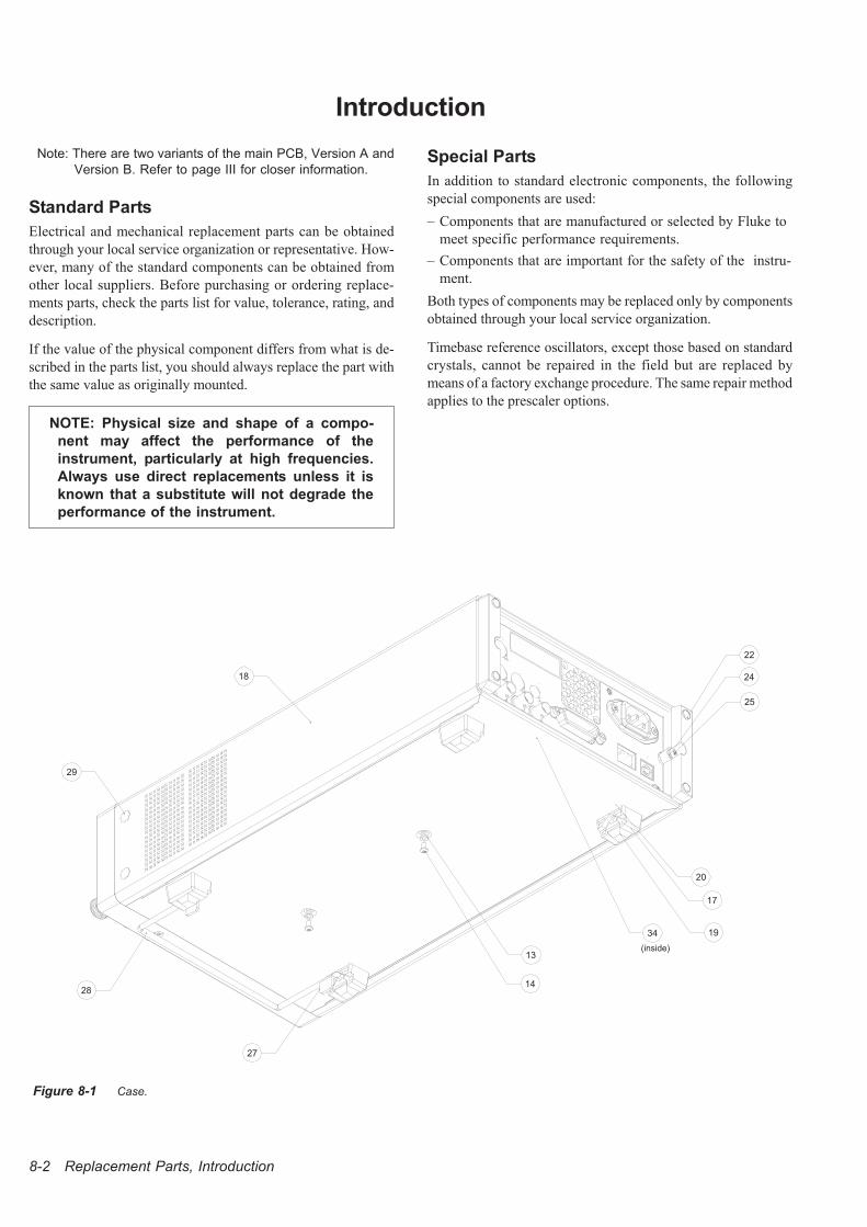
8-2 Replacement Parts, Introduction
Note: There are two variants of the main PCB, Version A and
Version B. Refer to page III for closer information.
Standard Parts
Electrical and mechanical replacement parts can be obtained
through your local service organization or representative. How-
ever, many of the standard components can be obtained from
other local suppliers. Before purchasing or ordering replace-
ments parts, check the parts list for value, tolerance, rating, and
description.
If the value of the physical component differs from what is de-
scribed in the parts list, you should always replace the part with
the same value as originally mounted.
NOTE: Physical size and shape of a compo-
nent may affect the performance of the
instrument, particularly at high frequencies.
Always use direct replacements unless it is
known that a substitute will not degrade the
performance of the instrument.
Special Parts
In addition to standard electronic components, the following
special components are used:
– Components that are manufactured or selected by Fluke to
meet specific performance requirements.
– Components that are important for the safety of the instru-
ment.
Both types of components may be replaced only by components
obtained through your local service organization.
Timebase reference oscillators, except those based on standard
crystals, cannot be repaired in the field but are replaced by
means of a factory exchange procedure. The same repair method
applies to the prescaler options.
22
25
2418
17
19
20
13
1428
27
29
34
(inside)
Figure 8-1 Case.
Introduction
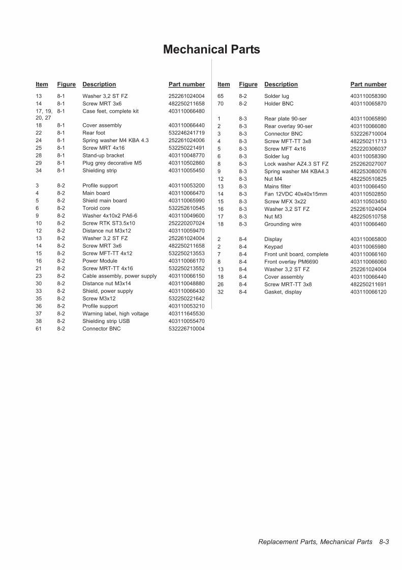
Item Figure Description Part number
13 8-1 Washer 3,2 ST FZ 252261024004
14 8-1 Screw MRT 3x6 482250211658
17, 19,
20, 27
8-1 Case feet, complete kit 403110066480
18 8-1 Cover assembly 403110066440
22 8-1 Rear foot 532246241719
24 8-1 Spring washer M4 KBA 4.3 252261024006
25 8-1 Screw MRT 4x16 532250221491
28 8-1 Stand-up bracket 403110048770
29 8-1 Plug grey decorative M5 403110502860
34 8-1 Shielding strip 403110055450
3 8-2 Profile support 403110053200
4 8-2 Main board 403110066470
5 8-2 Shield main board 403110065990
6 8-2 Toroid core 532252610545
9 8-2 Washer 4x10x2 PA6-6 403110049600
10 8-2 Screw RTK ST3.5x10 252220207024
12 8-2 Distance nut M3x12 403110059470
13 8-2 Washer 3,2 ST FZ 252261024004
14 8-2 Screw MRT 3x6 482250211658
15 8-2 Screw MFT-TT 4x12 532250213553
16 8-2 Power Module 403110066170
21 8-2 Screw MRT-TT 4x16 532250213552
23 8-2 Cable assembly, power supply 403110066150
30 8-2 Distance nut M3x14 403110048880
33 8-2 Shield, power supply 403110066430
35 8-2 Screw M3x12 532250221642
36 8-2 Profile support 403110053210
37 8-2 Warning label, high voltage 403111645530
38 8-2 Shielding strip USB 403110055470
61 8-2 Connector BNC 532226710004
Item Figure Description Part number
65 8-2 Solder lug 403110058390
70 8-2 Holder BNC 403110065870
1 8-3 Rear plate 90-ser 403110065890
2 8-3 Rear overlay 90-ser 403110066080
3 8-3 Connector BNC 532226710004
4 8-3 Screw MFT-TT 3x8 482250211713
5 8-3 Screw MFT 4x16 252220306037
6 8-3 Solder lug 403110058390
8 8-3 Lock washer AZ4.3 ST FZ 252262027007
9 8-3 Spring washer M4 KBA4.3 482253080076
12 8-3 Nut M4 482250510825
13 8-3 Mains filter 403110066450
14 8-3 Fan 12VDC 40x40x15mm 403110502850
15 8-3 Screw MFX 3x22 403110503450
16 8-3 Washer 3,2 ST FZ 252261024004
17 8-3 Nut M3 482250510758
18 8-3 Grounding wire 403110066460
2 8-4 Display 403110065800
2 8-4 Keypad 403110065980
7 8-4 Front unit board, complete 403110066160
8 8-4 Front overlay PM6690 403110066060
13 8-4 Washer 3,2 ST FZ 252261024004
18 8-4 Cover assembly 403110066440
26 8-4 Screw MRT-TT 3x8 482250211691
32 8-4 Gasket, display 403110066120
Replacement Parts, Mechanical Parts 8-3
Mechanical Parts
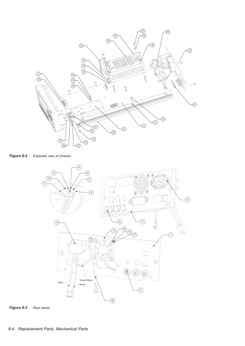
8-4 Replacement Parts, Mechanical Parts
6
9
4
5
15
10
14
13
23
12
14
13
15
314
13
30
33
37
21
3835
13
36
16
6
70
61
65
Figure 8-2 Exploded view of chassis.
6
1
8
12
9
23
4
5
9
12
13
8
18
BlueBrown
Green/Yellow
14
17
16
15
Figure 8-3 Rear panel.
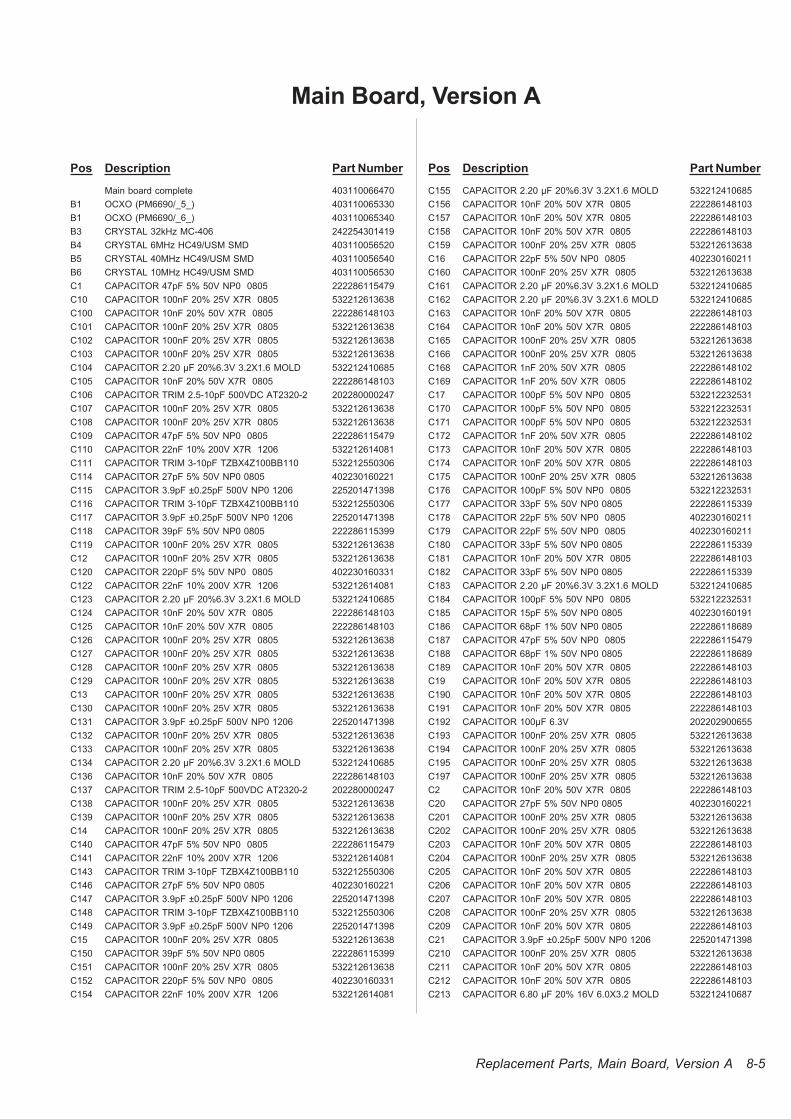
Pos Description Part Number
Main board complete 403110066470
B1 OCXO (PM6690/_5_) 403110065330
B1 OCXO (PM6690/_6_) 403110065340
B3 CRYSTAL 32kHz MC-406 242254301419
B4 CRYSTAL 6MHz HC49/USM SMD 403110056520
B5 CRYSTAL 40MHz HC49/USM SMD 403110056540
B6 CRYSTAL 10MHz HC49/USM SMD 403110056530
C1 CAPACITOR 47pF 5% 50V NP0 0805 222286115479
C10 CAPACITOR 100nF 20% 25V X7R 0805 532212613638
C100 CAPACITOR 10nF 20% 50V X7R 0805 222286148103
C101 CAPACITOR 100nF 20% 25V X7R 0805 532212613638
C102 CAPACITOR 100nF 20% 25V X7R 0805 532212613638
C103 CAPACITOR 100nF 20% 25V X7R 0805 532212613638
C104 CAPACITOR 2.20 µF 20%6.3V 3.2X1.6 MOLD 532212410685
C105 CAPACITOR 10nF 20% 50V X7R 0805 222286148103
C106 CAPACITOR TRIM 2.5-10pF 500VDC AT2320-2 202280000247
C107 CAPACITOR 100nF 20% 25V X7R 0805 532212613638
C108 CAPACITOR 100nF 20% 25V X7R 0805 532212613638
C109 CAPACITOR 47pF 5% 50V NP0 0805 222286115479
C110 CAPACITOR 22nF 10% 200V X7R 1206 532212614081
C111 CAPACITOR TRIM 3-10pF TZBX4Z100BB110 532212550306
C114 CAPACITOR 27pF 5% 50V NP0 0805 402230160221
C115 CAPACITOR 3.9pF ±0.25pF 500V NP0 1206 225201471398
C116 CAPACITOR TRIM 3-10pF TZBX4Z100BB110 532212550306
C117 CAPACITOR 3.9pF ±0.25pF 500V NP0 1206 225201471398
C118 CAPACITOR 39pF 5% 50V NP0 0805 222286115399
C119 CAPACITOR 100nF 20% 25V X7R 0805 532212613638
C12 CAPACITOR 100nF 20% 25V X7R 0805 532212613638
C120 CAPACITOR 220pF 5% 50V NP0 0805 402230160331
C122 CAPACITOR 22nF 10% 200V X7R 1206 532212614081
C123 CAPACITOR 2.20 µF 20%6.3V 3.2X1.6 MOLD 532212410685
C124 CAPACITOR 10nF 20% 50V X7R 0805 222286148103
C125 CAPACITOR 10nF 20% 50V X7R 0805 222286148103
C126 CAPACITOR 100nF 20% 25V X7R 0805 532212613638
C127 CAPACITOR 100nF 20% 25V X7R 0805 532212613638
C128 CAPACITOR 100nF 20% 25V X7R 0805 532212613638
C129 CAPACITOR 100nF 20% 25V X7R 0805 532212613638
C13 CAPACITOR 100nF 20% 25V X7R 0805 532212613638
C130 CAPACITOR 100nF 20% 25V X7R 0805 532212613638
C131 CAPACITOR 3.9pF ±0.25pF 500V NP0 1206 225201471398
C132 CAPACITOR 100nF 20% 25V X7R 0805 532212613638
C133 CAPACITOR 100nF 20% 25V X7R 0805 532212613638
C134 CAPACITOR 2.20 µF 20%6.3V 3.2X1.6 MOLD 532212410685
C136 CAPACITOR 10nF 20% 50V X7R 0805 222286148103
C137 CAPACITOR TRIM 2.5-10pF 500VDC AT2320-2 202280000247
C138 CAPACITOR 100nF 20% 25V X7R 0805 532212613638
C139 CAPACITOR 100nF 20% 25V X7R 0805 532212613638
C14 CAPACITOR 100nF 20% 25V X7R 0805 532212613638
C140 CAPACITOR 47pF 5% 50V NP0 0805 222286115479
C141 CAPACITOR 22nF 10% 200V X7R 1206 532212614081
C143 CAPACITOR TRIM 3-10pF TZBX4Z100BB110 532212550306
C146 CAPACITOR 27pF 5% 50V NP0 0805 402230160221
C147 CAPACITOR 3.9pF ±0.25pF 500V NP0 1206 225201471398
C148 CAPACITOR TRIM 3-10pF TZBX4Z100BB110 532212550306
C149 CAPACITOR 3.9pF ±0.25pF 500V NP0 1206 225201471398
C15 CAPACITOR 100nF 20% 25V X7R 0805 532212613638
C150 CAPACITOR 39pF 5% 50V NP0 0805 222286115399
C151 CAPACITOR 100nF 20% 25V X7R 0805 532212613638
C152 CAPACITOR 220pF 5% 50V NP0 0805 402230160331
C154 CAPACITOR 22nF 10% 200V X7R 1206 532212614081
Pos Description Part Number
C155 CAPACITOR 2.20 µF 20%6.3V 3.2X1.6 MOLD 532212410685
C156 CAPACITOR 10nF 20% 50V X7R 0805 222286148103
C157 CAPACITOR 10nF 20% 50V X7R 0805 222286148103
C158 CAPACITOR 10nF 20% 50V X7R 0805 222286148103
C159 CAPACITOR 100nF 20% 25V X7R 0805 532212613638
C16 CAPACITOR 22pF 5% 50V NP0 0805 402230160211
C160 CAPACITOR 100nF 20% 25V X7R 0805 532212613638
C161 CAPACITOR 2.20 µF 20%6.3V 3.2X1.6 MOLD 532212410685
C162 CAPACITOR 2.20 µF 20%6.3V 3.2X1.6 MOLD 532212410685
C163 CAPACITOR 10nF 20% 50V X7R 0805 222286148103
C164 CAPACITOR 10nF 20% 50V X7R 0805 222286148103
C165 CAPACITOR 100nF 20% 25V X7R 0805 532212613638
C166 CAPACITOR 100nF 20% 25V X7R 0805 532212613638
C168 CAPACITOR 1nF 20% 50V X7R 0805 222286148102
C169 CAPACITOR 1nF 20% 50V X7R 0805 222286148102
C17 CAPACITOR 100pF 5% 50V NP0 0805 532212232531
C170 CAPACITOR 100pF 5% 50V NP0 0805 532212232531
C171 CAPACITOR 100pF 5% 50V NP0 0805 532212232531
C172 CAPACITOR 1nF 20% 50V X7R 0805 222286148102
C173 CAPACITOR 10nF 20% 50V X7R 0805 222286148103
C174 CAPACITOR 10nF 20% 50V X7R 0805 222286148103
C175 CAPACITOR 100nF 20% 25V X7R 0805 532212613638
C176 CAPACITOR 100pF 5% 50V NP0 0805 532212232531
C177 CAPACITOR 33pF 5% 50V NP0 0805 222286115339
C178 CAPACITOR 22pF 5% 50V NP0 0805 402230160211
C179 CAPACITOR 22pF 5% 50V NP0 0805 402230160211
C180 CAPACITOR 33pF 5% 50V NP0 0805 222286115339
C181 CAPACITOR 10nF 20% 50V X7R 0805 222286148103
C182 CAPACITOR 33pF 5% 50V NP0 0805 222286115339
C183 CAPACITOR 2.20 µF 20%6.3V 3.2X1.6 MOLD 532212410685
C184 CAPACITOR 100pF 5% 50V NP0 0805 532212232531
C185 CAPACITOR 15pF 5% 50V NP0 0805 402230160191
C186 CAPACITOR 68pF 1% 50V NP0 0805 222286118689
C187 CAPACITOR 47pF 5% 50V NP0 0805 222286115479
C188 CAPACITOR 68pF 1% 50V NP0 0805 222286118689
C189 CAPACITOR 10nF 20% 50V X7R 0805 222286148103
C19 CAPACITOR 10nF 20% 50V X7R 0805 222286148103
C190 CAPACITOR 10nF 20% 50V X7R 0805 222286148103
C191 CAPACITOR 10nF 20% 50V X7R 0805 222286148103
C192 CAPACITOR 100µF 6.3V 202202900655
C193 CAPACITOR 100nF 20% 25V X7R 0805 532212613638
C194 CAPACITOR 100nF 20% 25V X7R 0805 532212613638
C195 CAPACITOR 100nF 20% 25V X7R 0805 532212613638
C197 CAPACITOR 100nF 20% 25V X7R 0805 532212613638
C2 CAPACITOR 10nF 20% 50V X7R 0805 222286148103
C20 CAPACITOR 27pF 5% 50V NP0 0805 402230160221
C201 CAPACITOR 100nF 20% 25V X7R 0805 532212613638
C202 CAPACITOR 100nF 20% 25V X7R 0805 532212613638
C203 CAPACITOR 10nF 20% 50V X7R 0805 222286148103
C204 CAPACITOR 100nF 20% 25V X7R 0805 532212613638
C205 CAPACITOR 10nF 20% 50V X7R 0805 222286148103
C206 CAPACITOR 10nF 20% 50V X7R 0805 222286148103
C207 CAPACITOR 10nF 20% 50V X7R 0805 222286148103
C208 CAPACITOR 100nF 20% 25V X7R 0805 532212613638
C209 CAPACITOR 10nF 20% 50V X7R 0805 222286148103
C21 CAPACITOR 3.9pF ±0.25pF 500V NP0 1206 225201471398
C210 CAPACITOR 100nF 20% 25V X7R 0805 532212613638
C211 CAPACITOR 10nF 20% 50V X7R 0805 222286148103
C212 CAPACITOR 10nF 20% 50V X7R 0805 222286148103
C213 CAPACITOR 6.80 µF 20% 16V 6.0X3.2 MOLD 532212410687
Replacement Parts, Main Board, Version A 8-5
Main Board, Version A
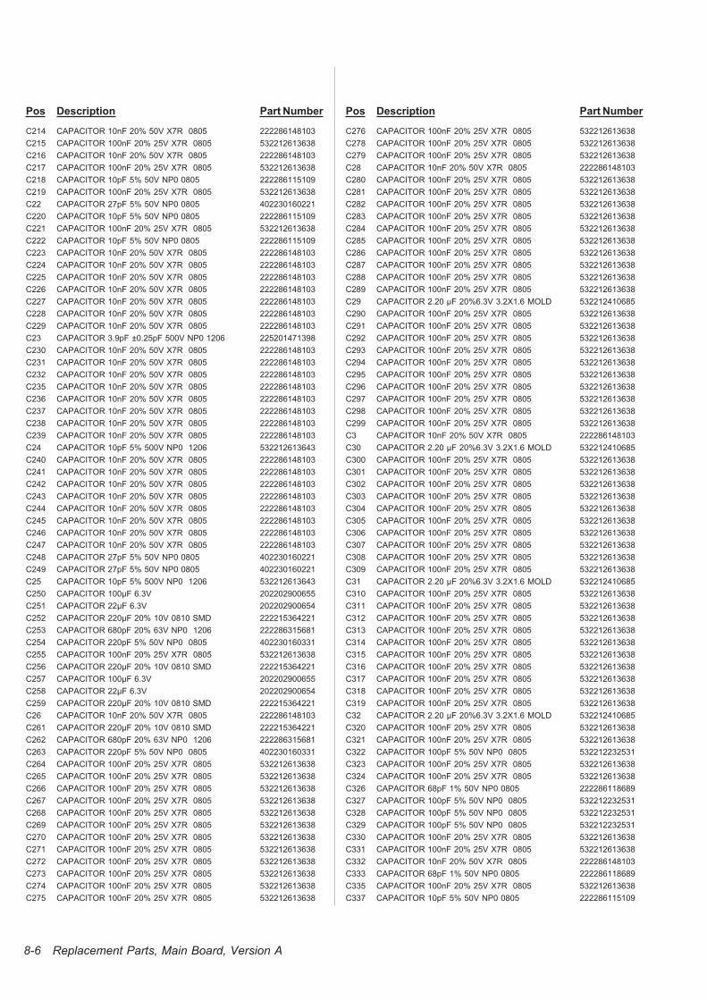
Pos Description Part Number
C214 CAPACITOR 10nF 20% 50V X7R 0805 222286148103
C215 CAPACITOR 100nF 20% 25V X7R 0805 532212613638
C216 CAPACITOR 10nF 20% 50V X7R 0805 222286148103
C217 CAPACITOR 100nF 20% 25V X7R 0805 532212613638
C218 CAPACITOR 10pF 5% 50V NP0 0805 222286115109
C219 CAPACITOR 100nF 20% 25V X7R 0805 532212613638
C22 CAPACITOR 27pF 5% 50V NP0 0805 402230160221
C220 CAPACITOR 10pF 5% 50V NP0 0805 222286115109
C221 CAPACITOR 100nF 20% 25V X7R 0805 532212613638
C222 CAPACITOR 10pF 5% 50V NP0 0805 222286115109
C223 CAPACITOR 10nF 20% 50V X7R 0805 222286148103
C224 CAPACITOR 10nF 20% 50V X7R 0805 222286148103
C225 CAPACITOR 10nF 20% 50V X7R 0805 222286148103
C226 CAPACITOR 10nF 20% 50V X7R 0805 222286148103
C227 CAPACITOR 10nF 20% 50V X7R 0805 222286148103
C228 CAPACITOR 10nF 20% 50V X7R 0805 222286148103
C229 CAPACITOR 10nF 20% 50V X7R 0805 222286148103
C23 CAPACITOR 3.9pF ±0.25pF 500V NP0 1206 225201471398
C230 CAPACITOR 10nF 20% 50V X7R 0805 222286148103
C231 CAPACITOR 10nF 20% 50V X7R 0805 222286148103
C232 CAPACITOR 10nF 20% 50V X7R 0805 222286148103
C235 CAPACITOR 10nF 20% 50V X7R 0805 222286148103
C236 CAPACITOR 10nF 20% 50V X7R 0805 222286148103
C237 CAPACITOR 10nF 20% 50V X7R 0805 222286148103
C238 CAPACITOR 10nF 20% 50V X7R 0805 222286148103
C239 CAPACITOR 10nF 20% 50V X7R 0805 222286148103
C24 CAPACITOR 10pF 5% 500V NP0 1206 532212613643
C240 CAPACITOR 10nF 20% 50V X7R 0805 222286148103
C241 CAPACITOR 10nF 20% 50V X7R 0805 222286148103
C242 CAPACITOR 10nF 20% 50V X7R 0805 222286148103
C243 CAPACITOR 10nF 20% 50V X7R 0805 222286148103
C244 CAPACITOR 10nF 20% 50V X7R 0805 222286148103
C245 CAPACITOR 10nF 20% 50V X7R 0805 222286148103
C246 CAPACITOR 10nF 20% 50V X7R 0805 222286148103
C247 CAPACITOR 10nF 20% 50V X7R 0805 222286148103
C248 CAPACITOR 27pF 5% 50V NP0 0805 402230160221
C249 CAPACITOR 27pF 5% 50V NP0 0805 402230160221
C25 CAPACITOR 10pF 5% 500V NP0 1206 532212613643
C250 CAPACITOR 100µF 6.3V 202202900655
C251 CAPACITOR 22µF 6.3V 202202900654
C252 CAPACITOR 220µF 20% 10V 0810 SMD 222215364221
C253 CAPACITOR 680pF 20% 63V NP0 1206 222286315681
C254 CAPACITOR 220pF 5% 50V NP0 0805 402230160331
C255 CAPACITOR 100nF 20% 25V X7R 0805 532212613638
C256 CAPACITOR 220µF 20% 10V 0810 SMD 222215364221
C257 CAPACITOR 100µF 6.3V 202202900655
C258 CAPACITOR 22µF 6.3V 202202900654
C259 CAPACITOR 220µF 20% 10V 0810 SMD 222215364221
C26 CAPACITOR 10nF 20% 50V X7R 0805 222286148103
C261 CAPACITOR 220µF 20% 10V 0810 SMD 222215364221
C262 CAPACITOR 680pF 20% 63V NP0 1206 222286315681
C263 CAPACITOR 220pF 5% 50V NP0 0805 402230160331
C264 CAPACITOR 100nF 20% 25V X7R 0805 532212613638
C265 CAPACITOR 100nF 20% 25V X7R 0805 532212613638
C266 CAPACITOR 100nF 20% 25V X7R 0805 532212613638
C267 CAPACITOR 100nF 20% 25V X7R 0805 532212613638
C268 CAPACITOR 100nF 20% 25V X7R 0805 532212613638
C269 CAPACITOR 100nF 20% 25V X7R 0805 532212613638
C270 CAPACITOR 100nF 20% 25V X7R 0805 532212613638
C271 CAPACITOR 100nF 20% 25V X7R 0805 532212613638
C272 CAPACITOR 100nF 20% 25V X7R 0805 532212613638
C273 CAPACITOR 100nF 20% 25V X7R 0805 532212613638
C274 CAPACITOR 100nF 20% 25V X7R 0805 532212613638
C275 CAPACITOR 100nF 20% 25V X7R 0805 532212613638
Pos Description Part Number
C276 CAPACITOR 100nF 20% 25V X7R 0805 532212613638
C278 CAPACITOR 100nF 20% 25V X7R 0805 532212613638
C279 CAPACITOR 100nF 20% 25V X7R 0805 532212613638
C28 CAPACITOR 10nF 20% 50V X7R 0805 222286148103
C280 CAPACITOR 100nF 20% 25V X7R 0805 532212613638
C281 CAPACITOR 100nF 20% 25V X7R 0805 532212613638
C282 CAPACITOR 100nF 20% 25V X7R 0805 532212613638
C283 CAPACITOR 100nF 20% 25V X7R 0805 532212613638
C284 CAPACITOR 100nF 20% 25V X7R 0805 532212613638
C285 CAPACITOR 100nF 20% 25V X7R 0805 532212613638
C286 CAPACITOR 100nF 20% 25V X7R 0805 532212613638
C287 CAPACITOR 100nF 20% 25V X7R 0805 532212613638
C288 CAPACITOR 100nF 20% 25V X7R 0805 532212613638
C289 CAPACITOR 100nF 20% 25V X7R 0805 532212613638
C29 CAPACITOR 2.20 µF 20%6.3V 3.2X1.6 MOLD 532212410685
C290 CAPACITOR 100nF 20% 25V X7R 0805 532212613638
C291 CAPACITOR 100nF 20% 25V X7R 0805 532212613638
C292 CAPACITOR 100nF 20% 25V X7R 0805 532212613638
C293 CAPACITOR 100nF 20% 25V X7R 0805 532212613638
C294 CAPACITOR 100nF 20% 25V X7R 0805 532212613638
C295 CAPACITOR 100nF 20% 25V X7R 0805 532212613638
C296 CAPACITOR 100nF 20% 25V X7R 0805 532212613638
C297 CAPACITOR 100nF 20% 25V X7R 0805 532212613638
C298 CAPACITOR 100nF 20% 25V X7R 0805 532212613638
C299 CAPACITOR 100nF 20% 25V X7R 0805 532212613638
C3 CAPACITOR 10nF 20% 50V X7R 0805 222286148103
C30 CAPACITOR 2.20 µF 20%6.3V 3.2X1.6 MOLD 532212410685
C300 CAPACITOR 100nF 20% 25V X7R 0805 532212613638
C301 CAPACITOR 100nF 20% 25V X7R 0805 532212613638
C302 CAPACITOR 100nF 20% 25V X7R 0805 532212613638
C303 CAPACITOR 100nF 20% 25V X7R 0805 532212613638
C304 CAPACITOR 100nF 20% 25V X7R 0805 532212613638
C305 CAPACITOR 100nF 20% 25V X7R 0805 532212613638
C306 CAPACITOR 100nF 20% 25V X7R 0805 532212613638
C307 CAPACITOR 100nF 20% 25V X7R 0805 532212613638
C308 CAPACITOR 100nF 20% 25V X7R 0805 532212613638
C309 CAPACITOR 100nF 20% 25V X7R 0805 532212613638
C31 CAPACITOR 2.20 µF 20%6.3V 3.2X1.6 MOLD 532212410685
C310 CAPACITOR 100nF 20% 25V X7R 0805 532212613638
C311 CAPACITOR 100nF 20% 25V X7R 0805 532212613638
C312 CAPACITOR 100nF 20% 25V X7R 0805 532212613638
C313 CAPACITOR 100nF 20% 25V X7R 0805 532212613638
C314 CAPACITOR 100nF 20% 25V X7R 0805 532212613638
C315 CAPACITOR 100nF 20% 25V X7R 0805 532212613638
C316 CAPACITOR 100nF 20% 25V X7R 0805 532212613638
C317 CAPACITOR 100nF 20% 25V X7R 0805 532212613638
C318 CAPACITOR 100nF 20% 25V X7R 0805 532212613638
C319 CAPACITOR 100nF 20% 25V X7R 0805 532212613638
C32 CAPACITOR 2.20 µF 20%6.3V 3.2X1.6 MOLD 532212410685
C320 CAPACITOR 100nF 20% 25V X7R 0805 532212613638
C321 CAPACITOR 100nF 20% 25V X7R 0805 532212613638
C322 CAPACITOR 100pF 5% 50V NP0 0805 532212232531
C323 CAPACITOR 100nF 20% 25V X7R 0805 532212613638
C324 CAPACITOR 100nF 20% 25V X7R 0805 532212613638
C326 CAPACITOR 68pF 1% 50V NP0 0805 222286118689
C327 CAPACITOR 100pF 5% 50V NP0 0805 532212232531
C328 CAPACITOR 100pF 5% 50V NP0 0805 532212232531
C329 CAPACITOR 100pF 5% 50V NP0 0805 532212232531
C330 CAPACITOR 100nF 20% 25V X7R 0805 532212613638
C331 CAPACITOR 100nF 20% 25V X7R 0805 532212613638
C332 CAPACITOR 10nF 20% 50V X7R 0805 222286148103
C333 CAPACITOR 68pF 1% 50V NP0 0805 222286118689
C335 CAPACITOR 100nF 20% 25V X7R 0805 532212613638
C337 CAPACITOR 10pF 5% 50V NP0 0805 222286115109
8-6 Replacement Parts, Main Board, Version A
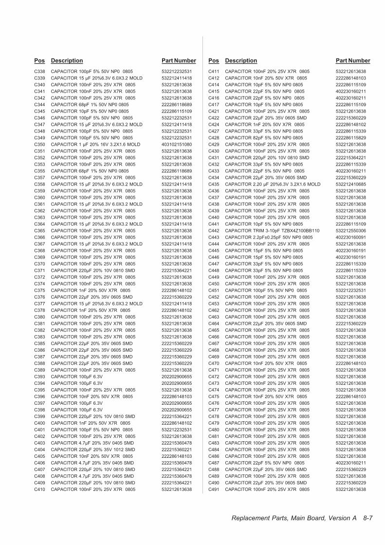
Pos Description Part Number
C338 CAPACITOR 100pF 5% 50V NP0 0805 532212232531
C339 CAPACITOR 15 µF 20%6.3V 6.0X3.2 MOLD 532212411418
C340 CAPACITOR 100nF 20% 25V X7R 0805 532212613638
C341 CAPACITOR 100nF 20% 25V X7R 0805 532212613638
C342 CAPACITOR 100nF 20% 25V X7R 0805 532212613638
C344 CAPACITOR 68pF 1% 50V NP0 0805 222286118689
C345 CAPACITOR 10pF 5% 50V NP0 0805 222286115109
C346 CAPACITOR 100pF 5% 50V NP0 0805 532212232531
C347 CAPACITOR 15 µF 20%6.3V 6.0X3.2 MOLD 532212411418
C348 CAPACITOR 100pF 5% 50V NP0 0805 532212232531
C349 CAPACITOR 100pF 5% 50V NP0 0805 532212232531
C350 CAPACITOR 1 µF 20% 16V 3.2X1.6 MOLD 403102151080
C351 CAPACITOR 100nF 20% 25V X7R 0805 532212613638
C352 CAPACITOR 100nF 20% 25V X7R 0805 532212613638
C353 CAPACITOR 100nF 20% 25V X7R 0805 532212613638
C355 CAPACITOR 68pF 1% 50V NP0 0805 222286118689
C357 CAPACITOR 100nF 20% 25V X7R 0805 532212613638
C358 CAPACITOR 15 µF 20%6.3V 6.0X3.2 MOLD 532212411418
C359 CAPACITOR 100nF 20% 25V X7R 0805 532212613638
C360 CAPACITOR 100nF 20% 25V X7R 0805 532212613638
C361 CAPACITOR 15 µF 20%6.3V 6.0X3.2 MOLD 532212411418
C362 CAPACITOR 100nF 20% 25V X7R 0805 532212613638
C363 CAPACITOR 100nF 20% 25V X7R 0805 532212613638
C364 CAPACITOR 15 µF 20%6.3V 6.0X3.2 MOLD 532212411418
C365 CAPACITOR 100nF 20% 25V X7R 0805 532212613638
C366 CAPACITOR 100nF 20% 25V X7R 0805 532212613638
C367 CAPACITOR 15 µF 20%6.3V 6.0X3.2 MOLD 532212411418
C368 CAPACITOR 100nF 20% 25V X7R 0805 532212613638
C369 CAPACITOR 100nF 20% 25V X7R 0805 532212613638
C370 CAPACITOR 100nF 20% 25V X7R 0805 532212613638
C371 CAPACITOR 220µF 20% 10V 0810 SMD 222215364221
C372 CAPACITOR 100nF 20% 25V X7R 0805 532212613638
C374 CAPACITOR 100nF 20% 25V X7R 0805 532212613638
C375 CAPACITOR 1nF 20% 50V X7R 0805 222286148102
C376 CAPACITOR 22µF 20% 35V 0605 SMD 222215360229
C377 CAPACITOR 15 µF 20%6.3V 6.0X3.2 MOLD 532212411418
C378 CAPACITOR 1nF 20% 50V X7R 0805 222286148102
C380 CAPACITOR 100nF 20% 25V X7R 0805 532212613638
C381 CAPACITOR 100nF 20% 25V X7R 0805 532212613638
C382 CAPACITOR 100nF 20% 25V X7R 0805 532212613638
C383 CAPACITOR 100nF 20% 25V X7R 0805 532212613638
C385 CAPACITOR 22µF 20% 35V 0605 SMD 222215360229
C386 CAPACITOR 22µF 20% 35V 0605 SMD 222215360229
C387 CAPACITOR 22µF 20% 35V 0605 SMD 222215360229
C388 CAPACITOR 22µF 20% 35V 0605 SMD 222215360229
C389 CAPACITOR 100nF 20% 25V X7R 0805 532212613638
C393 CAPACITOR 100µF 6.3V 202202900655
C394 CAPACITOR 100µF 6.3V 202202900655
C395 CAPACITOR 100nF 20% 25V X7R 0805 532212613638
C396 CAPACITOR 10nF 20% 50V X7R 0805 222286148103
C397 CAPACITOR 100µF 6.3V 202202900655
C398 CAPACITOR 100µF 6.3V 202202900655
C399 CAPACITOR 220µF 20% 10V 0810 SMD 222215364221
C400 CAPACITOR 1nF 20% 50V X7R 0805 222286148102
C401 CAPACITOR 100pF 5% 50V NP0 0805 532212232531
C402 CAPACITOR 100nF 20% 25V X7R 0805 532212613638
C403 CAPACITOR 4.7µF 20% 35V 0405 SMD 222215360478
C404 CAPACITOR 220µF 20% 35V 1012 SMD 222215360221
C405 CAPACITOR 10nF 20% 50V X7R 0805 222286148103
C406 CAPACITOR 4.7µF 20% 35V 0405 SMD 222215360478
C407 CAPACITOR 220µF 20% 10V 0810 SMD 222215364221
C408 CAPACITOR 4.7µF 20% 35V 0405 SMD 222215360478
C409 CAPACITOR 220µF 20% 10V 0810 SMD 222215364221
C410 CAPACITOR 100nF 20% 25V X7R 0805 532212613638
Pos Description Part Number
C411 CAPACITOR 100nF 20% 25V X7R 0805 532212613638
C412 CAPACITOR 10nF 20% 50V X7R 0805 222286148103
C414 CAPACITOR 10pF 5% 50V NP0 0805 222286115109
C415 CAPACITOR 22pF 5% 50V NP0 0805 402230160211
C416 CAPACITOR 22pF 5% 50V NP0 0805 402230160211
C417 CAPACITOR 10pF 5% 50V NP0 0805 222286115109
C421 CAPACITOR 100nF 20% 25V X7R 0805 532212613638
C422 CAPACITOR 22µF 20% 35V 0605 SMD 222215360229
C424 CAPACITOR 1nF 20% 50V X7R 0805 222286148102
C427 CAPACITOR 33pF 5% 50V NP0 0805 222286115339
C428 CAPACITOR 82pF 5% 50V NP0 0805 222286115829
C429 CAPACITOR 100nF 20% 25V X7R 0805 532212613638
C430 CAPACITOR 100nF 20% 25V X7R 0805 532212613638
C431 CAPACITOR 220µF 20% 10V 0810 SMD 222215364221
C432 CAPACITOR 33pF 5% 50V NP0 0805 222286115339
C433 CAPACITOR 22pF 5% 50V NP0 0805 402230160211
C434 CAPACITOR 22µF 20% 35V 0605 SMD 222215360229
C435 CAPACITOR 2.20 µF 20%6.3V 3.2X1.6 MOLD 532212410685
C436 CAPACITOR 100nF 20% 25V X7R 0805 532212613638
C437 CAPACITOR 100nF 20% 25V X7R 0805 532212613638
C438 CAPACITOR 100nF 20% 25V X7R 0805 532212613638
C439 CAPACITOR 100nF 20% 25V X7R 0805 532212613638
C440 CAPACITOR 100nF 20% 25V X7R 0805 532212613638
C441 CAPACITOR 10pF 5% 50V NP0 0805 222286115109
C442 CAPACITOR TRIM 3-10pF TZBX4Z100BB110 532212550306
C443 CAPACITOR 2.2pF±0.25pF 50V NP0 0805 402230160091
C444 CAPACITOR 100nF 20% 25V X7R 0805 532212613638
C445 CAPACITOR 15pF 5% 50V NP0 0805 402230160191
C446 CAPACITOR 15pF 5% 50V NP0 0805 402230160191
C447 CAPACITOR 33pF 5% 50V NP0 0805 222286115339
C448 CAPACITOR 33pF 5% 50V NP0 0805 222286115339
C449 CAPACITOR 100nF 20% 25V X7R 0805 532212613638
C450 CAPACITOR 100nF 20% 25V X7R 0805 532212613638
C451 CAPACITOR 100pF 5% 50V NP0 0805 532212232531
C452 CAPACITOR 100nF 20% 25V X7R 0805 532212613638
C453 CAPACITOR 100nF 20% 25V X7R 0805 532212613638
C462 CAPACITOR 100nF 20% 25V X7R 0805 532212613638
C463 CAPACITOR 100nF 20% 25V X7R 0805 532212613638
C464 CAPACITOR 22µF 20% 35V 0605 SMD 222215360229
C465 CAPACITOR 100nF 20% 25V X7R 0805 532212613638
C466 CAPACITOR 100nF 20% 25V X7R 0805 532212613638
C467 CAPACITOR 100nF 20% 25V X7R 0805 532212613638
C468 CAPACITOR 100nF 20% 25V X7R 0805 532212613638
C469 CAPACITOR 100nF 20% 25V X7R 0805 532212613638
C470 CAPACITOR 10nF 20% 50V X7R 0805 222286148103
C471 CAPACITOR 100nF 20% 25V X7R 0805 532212613638
C472 CAPACITOR 100nF 20% 25V X7R 0805 532212613638
C473 CAPACITOR 100nF 20% 25V X7R 0805 532212613638
C474 CAPACITOR 100nF 20% 25V X7R 0805 532212613638
C475 CAPACITOR 10nF 20% 50V X7R 0805 222286148103
C476 CAPACITOR 100nF 20% 25V X7R 0805 532212613638
C477 CAPACITOR 100nF 20% 25V X7R 0805 532212613638
C478 CAPACITOR 100nF 20% 25V X7R 0805 532212613638
C479 CAPACITOR 100nF 20% 25V X7R 0805 532212613638
C480 CAPACITOR 100nF 20% 25V X7R 0805 532212613638
C481 CAPACITOR 100nF 20% 25V X7R 0805 532212613638
C483 CAPACITOR 100nF 20% 25V X7R 0805 532212613638
C484 CAPACITOR 100nF 20% 25V X7R 0805 532212613638
C486 CAPACITOR 100nF 20% 25V X7R 0805 532212613638
C487 CAPACITOR 22pF 5% 50V NP0 0805 402230160211
C488 CAPACITOR 22µF 20% 35V 0605 SMD 222215360229
C489 CAPACITOR 100nF 20% 25V X7R 0805 532212613638
C490 CAPACITOR 22µF 20% 35V 0605 SMD 222215360229
C491 CAPACITOR 100nF 20% 25V X7R 0805 532212613638
Replacement Parts, Main Board, Version A 8-7
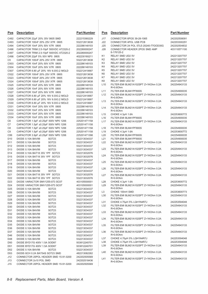
Pos Description Part Number
C492 CAPACITOR 22µF 20% 35V 0605 SMD 222215360229
C493 CAPACITOR 100nF 20% 25V X7R 0805 532212613638
C494 CAPACITOR 10nF 20% 50V X7R 0805 222286148103
C496 CAPACITOR TRIM 2.5-10pF 500VDC AT2320-2 202280000247
C497 CAPACITOR TRIM 2.5-10pF 500VDC AT2320-2 202280000247
C498 CAPACITOR 22pF 5% 50V NP0 0805 402230160211
C5 CAPACITOR 100nF 20% 25V X7R 0805 532212613638
C503 CAPACITOR 10nF 20% 50V X7R 0805 222286148103
C504 CAPACITOR 10nF 20% 50V X7R 0805 222286148103
C507 CAPACITOR 6.80 µF 20% 16V 6.0X3.2 MOLD 532212410687
C522 CAPACITOR 100nF 20% 25V X7R 0805 532212613638
C523 CAPACITOR 100nF 20% 25V X7R 0805 532212613638
C524 CAPACITOR 100nF 20% 25V X7R 0805 532212613638
C525 CAPACITOR 10nF 20% 50V X7R 0805 222286148103
C526 CAPACITOR 10nF 20% 50V X7R 0805 222286148103
C527 CAPACITOR 10nF 20% 50V X7R 0805 222286148103
C528 CAPACITOR 6.80 µF 20% 16V 6.0X3.2 MOLD 532212410687
C529 CAPACITOR 6.80 µF 20% 16V 6.0X3.2 MOLD 532212410687
C530 CAPACITOR 6.80 µF 20% 16V 6.0X3.2 MOLD 532212410687
C531 CAPACITOR 10nF 20% 50V X7R 0805 222286148103
C532 CAPACITOR 10nF 20% 50V X7R 0805 222286148103
C533 CAPACITOR 10nF 20% 50V X7R 0805 222286148103
C534 CAPACITOR 10nF 20% 50V X7R 0805 222286148103
C6 CAPACITOR 1.5pF ±0.25pF 500V NP0 1206 225201471158
C7 CAPACITOR 1.5pF ±0.25pF 500V NP0 1206 225201471158
C8 CAPACITOR 1.5pF ±0.25pF 500V NP0 1206 225201471158
C9 CAPACITOR 1.5pF ±0.25pF 500V NP0 1206 225201471158
C99 CAPACITOR 3.9pF ±0.25pF 500V NP0 1206 225201471398
D10 DIODE 0.10A BAV99 SOT23 532213034337
D11 DIODE 0.10A BAV99 SOT23 532213034337
D12 DIODE 0.10A BAV99 SOT23 532213034337
D13 DIODE 0.10A BAV99 SOT23 532213034337
D14 DIODE 0.10A BAT18 35V 1PF SOT23 532213032076
D15 DIODE 0.10A BAT18 35V 1PF SOT23 532213032076
D17 DIODE 0.10A BAV99 SOT23 532213034337
D18 DIODE 0.10A BAV99 SOT23 532213034337
D19 DIODE 0.10A BAV99 SOT23 532213034337
D20 DIODE 0.10A BAV99 SOT23 532213034337
D21 DIODE 0.10A BAT18 35V 1PF SOT23 532213032076
D22 DIODE 0.10A BAT18 35V 1PF SOT23 532213032076
D23 DIODE VARACTOR SMV1255-073 SC07 403105000001
D24 DIODE VARACTOR SMV1255-073 SC07 403105000001
D25 DIODE 0.10A BAV99 SOT23 532213034337
D26 DIODE 0.10A BAV99 SOT23 532213034337
D27 DIODE 0.10A BAV99 SOT23 532213034337
D28 DIODE 0.10A BAV99 SOT23 532213034337
D29 DIODE 0.10A BAV99 SOT23 532213034337
D30 DIODE 0.10A BAV99 SOT23 532213034337
D31 DIODE 0.10A BAV99 SOT23 532213034337
D32 DIODE 0.10A BAV99 SOT23 532213034337
D33 DIODE 0.10A BAV99 SOT23 532213034337
D34 DIODE 0.10A BAV99 SOT23 532213034337
D35 DIODE 0.10A BAV99 SOT23 532213034337
D36 DIODE 0.10A BAV99 SOT23 532213034337
D37 DIODE 0.10A BAV99 SOT23 532213034337
D46 DIODE 0.10A BAV99 SOT23 532213034337
D48 DIODE 0.10A BAV99 SOT23 532213034337
D50 DIODE BYD17G 400V 1.5A SOD87 933812240701
D51 DIODE BYD17G 400V 1.5A SOD87 933812240701
D52 DIODE 0.10A BAV99 SOT23 532213034337
D53 DIODE-SCH 0.2A BAT54S SOT23 SMD 482213082262
J12 CONNECTOR 20POL HEADER SMD 15-91-0200 242202505569
J13 CONNECTOR 2x10 POL SMD 242202518436
J15 CONNECTOR 20POL HEADER SMD 15-91-0200 242202505569
Pos Description Part Number
J17 CONNECTOR 6POS 39-28-1065 242202508091
J22 CONNECTOR 4POL USB PCB 242203300291
J25 CONNECTOR 24 POL 57LE-20240-77OOD35G 242202504832
J28 CONNECTOR HEADER 2POS SMD AMP
6-176125-2
403110571100
K1 RELAY SMD UD2 5V 242213207707
K2 RELAY SMD UD2 5V 242213207707
K3 RELAY SMD UD2 5V 242213207707
K4 RELAY SMD UD2 5V 242213207707
K5 RELAY SMD UD2 5V 242213207707
K6 RELAY SMD UD2 5V 242213207707
K7 RELAY SMD UD2 5V 242213207707
K8 RELAY SMD UD2 5V 242213207707
L10 FILTER-EMI BLM21A102SPT Z=1KOhm 0.2A
R=0.6Ohm
242254943133
L11 FILTER-EMI BLM41PF800S 242254900035
L12 FILTER-EMI BLM21A102SPT Z=1KOhm 0.2A
R=0.6Ohm
242254943133
L13 FILTER-EMI BLM21A102SPT Z=1KOhm 0.2A
R=0.6Ohm
242254943133
L14 FILTER-EMI BLM21A102SPT Z=1KOhm 0.2A
R=0.6Ohm
242254943133
L15 CHOKE 4.3µH 1.6A 242253600772
L16 FILTER-EMI BLM41PF800S 242254900035
L17 FILTER-EMI BLM21A102SPT Z=1KOhm 0.2A
R=0.6Ohm
242254943133
L18 FILTER-EMI BLM41PF800S 242254900035
L19 CHOKE 4.3µH 1.6A 242253600772
L20 FILTER-EMI BLM41PF800S 242254900035
L21 FILTER-EMI BLM41PF800S 242254900035
L22 FILTER-EMI BLM21A102SPT Z=1KOhm 0.2A
R=0.6Ohm
242254943133
L23 FILTER-EMI BLM21A102SPT Z=1KOhm 0.2A
R=0.6Ohm
242254943133
L24 FILTER-EMI BLM21A102SPT Z=1KOhm 0.2A
R=0.6Ohm
242254943133
L25 FILTER-EMI BLM21A102SPT Z=1KOhm 0.2A
R=0.6Ohm
242254943133
L26 FILTER-EMI BLM21A102SPT Z=1KOhm 0.2A
R=0.6Ohm
242254943133
L27 FILTER-EMI BLM21A102SPT Z=1KOhm 0.2A
R=0.6Ohm
242254943133
L28 CHOKE 4.3µH 1.6A 242253600772
L29 FILTER-EMI BLM21A102SPT Z=1KOhm 0.2A
R=0.6Ohm
242254943133
L3 CHOKE 100nH SMD 242253600773
L30 FILTER-EMI BLM21A102SPT Z=1KOhm 0.2A
R=0.6Ohm
242254943133
L31 CHOKE 4.70µH 5% LQH1N4R7J 242253594048
L32 FILTER-EMI BLM21A102SPT Z=1KOhm 0.2A
R=0.6Ohm
242254943133
L33 FILTER-EMI BLM21A102SPT Z=1KOhm 0.2A
R=0.6Ohm
242254943133
L34 FILTER-EMI BLM21A102SPT Z=1KOhm 0.2A
R=0.6Ohm
242254943133
L35 FILTER-EMI BLM21A102SPT Z=1KOhm 0.2A
R=0.6Ohm
242254943133
L36 FILTER-EMI BLM21A102SPT Z=1KOhm 0.2A
R=0.6Ohm
242254943133
L37 CHOKE 4.70µH 5% LQH1N4R7J 242253594048
L38 CHOKE 4.70µH 5% LQH1N4R7J 242253594048
L39 FILTER-EMI BLM21A102SPT Z=1KOhm 0.2A
R=0.6Ohm
242254943133
L40 FILTER-EMI BLM21A102SPT Z=1KOhm 0.2A
R=0.6Ohm
242254943133
L41 FILTER-EMI BLM21A102SPT Z=1KOhm 0.2A
R=0.6Ohm
242254943133
8-8 Replacement Parts, Main Board, Version A
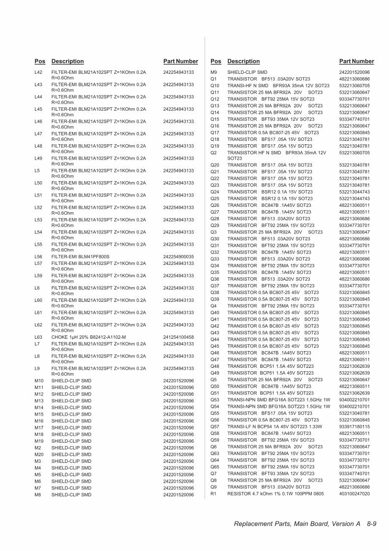
Pos Description Part Number
L42 FILTER-EMI BLM21A102SPT Z=1KOhm 0.2A
R=0.6Ohm
242254943133
L43 FILTER-EMI BLM21A102SPT Z=1KOhm 0.2A
R=0.6Ohm
242254943133
L44 FILTER-EMI BLM21A102SPT Z=1KOhm 0.2A
R=0.6Ohm
242254943133
L45 FILTER-EMI BLM21A102SPT Z=1KOhm 0.2A
R=0.6Ohm
242254943133
L46 FILTER-EMI BLM21A102SPT Z=1KOhm 0.2A
R=0.6Ohm
242254943133
L47 FILTER-EMI BLM21A102SPT Z=1KOhm 0.2A
R=0.6Ohm
242254943133
L48 FILTER-EMI BLM21A102SPT Z=1KOhm 0.2A
R=0.6Ohm
242254943133
L49 FILTER-EMI BLM21A102SPT Z=1KOhm 0.2A
R=0.6Ohm
242254943133
L5 FILTER-EMI BLM21A102SPT Z=1KOhm 0.2A
R=0.6Ohm
242254943133
L50 FILTER-EMI BLM21A102SPT Z=1KOhm 0.2A
R=0.6Ohm
242254943133
L51 FILTER-EMI BLM21A102SPT Z=1KOhm 0.2A
R=0.6Ohm
242254943133
L52 FILTER-EMI BLM21A102SPT Z=1KOhm 0.2A
R=0.6Ohm
242254943133
L53 FILTER-EMI BLM21A102SPT Z=1KOhm 0.2A
R=0.6Ohm
242254943133
L54 FILTER-EMI BLM21A102SPT Z=1KOhm 0.2A
R=0.6Ohm
242254943133
L55 FILTER-EMI BLM21A102SPT Z=1KOhm 0.2A
R=0.6Ohm
242254943133
L56 FILTER-EMI BLM41PF800S 242254900035
L57 FILTER-EMI BLM21A102SPT Z=1KOhm 0.2A
R=0.6Ohm
242254943133
L59 FILTER-EMI BLM21A102SPT Z=1KOhm 0.2A
R=0.6Ohm
242254943133
L6 FILTER-EMI BLM21A102SPT Z=1KOhm 0.2A
R=0.6Ohm
242254943133
L60 FILTER-EMI BLM21A102SPT Z=1KOhm 0.2A
R=0.6Ohm
242254943133
L61 FILTER-EMI BLM21A102SPT Z=1KOhm 0.2A
R=0.6Ohm
242254943133
L62 FILTER-EMI BLM21A102SPT Z=1KOhm 0.2A
R=0.6Ohm
242254943133
L63 CHOKE 1µH 20% B82412-A1102-M 241254100458
L7 FILTER-EMI BLM21A102SPT Z=1KOhm 0.2A
R=0.6Ohm
242254943133
L8 FILTER-EMI BLM21A102SPT Z=1KOhm 0.2A
R=0.6Ohm
242254943133
L9 FILTER-EMI BLM21A102SPT Z=1KOhm 0.2A
R=0.6Ohm
242254943133
M10 SHIELD-CLIP SMD 242201520096
M11 SHIELD-CLIP SMD 242201520096
M12 SHIELD-CLIP SMD 242201520096
M13 SHIELD-CLIP SMD 242201520096
M14 SHIELD-CLIP SMD 242201520096
M15 SHIELD-CLIP SMD 242201520096
M16 SHIELD-CLIP SMD 242201520096
M17 SHIELD-CLIP SMD 242201520096
M18 SHIELD-CLIP SMD 242201520096
M19 SHIELD-CLIP SMD 242201520096
M2 SHIELD-CLIP SMD 242201520096
M20 SHIELD-CLIP SMD 242201520096
M3 SHIELD-CLIP SMD 242201520096
M4 SHIELD-CLIP SMD 242201520096
M5 SHIELD-CLIP SMD 242201520096
M6 SHIELD-CLIP SMD 242201520096
M7 SHIELD-CLIP SMD 242201520096
M8 SHIELD-CLIP SMD 242201520096
Pos Description Part Number
M9 SHIELD-CLIP SMD 242201520096
Q1 TRANSISTOR BF513 .03A20V SOT23 482213060686
Q10 TRANSI-HF N SMD BFR93A 35mA 12V SOT23 532213060705
Q11 TRANSISTOR 25 MA BFR92A 20V SOT23 532213060647
Q12 TRANSISTOR BFT92 25MA 15V SOT23 933347730701
Q13 TRANSISTOR 25 MA BFR92A 20V SOT23 532213060647
Q14 TRANSISTOR 25 MA BFR92A 20V SOT23 532213060647
Q15 TRANSISTOR BFT93 35MA 12V SOT23 933347740701
Q16 TRANSISTOR 25 MA BFR92A 20V SOT23 532213060647
Q17 TRANSISTOR 0.5A BC807-25 45V SOT23 532213060845
Q18 TRANSISTOR BFS17 .05A 15V SOT23 532213040781
Q19 TRANSISTOR BFS17 .05A 15V SOT23 532213040781
Q2 TRANSISTOR HF N SMD BFR93A 35mA 12V
SOT23
532213060705
Q20 TRANSISTOR BFS17 .05A 15V SOT23 532213040781
Q21 TRANSISTOR BFS17 .05A 15V SOT23 532213040781
Q22 TRANSISTOR BFS17 .05A 15V SOT23 532213040781
Q23 TRANSISTOR BFS17 .05A 15V SOT23 532213040781
Q24 TRANSISTOR BSR12 0.1A 15V SOT23 532213044743
Q25 TRANSISTOR BSR12 0.1A 15V SOT23 532213044743
Q26 TRANSISTOR BC847B .1A45V SOT23 482213060511
Q27 TRANSISTOR BC847B .1A45V SOT23 482213060511
Q28 TRANSISTOR BF513 .03A20V SOT23 482213060686
Q29 TRANSISTOR BFT92 25MA 15V SOT23 933347730701
Q3 TRANSISTOR 25 MA BFR92A 20V SOT23 532213060647
Q30 TRANSISTOR BF513 .03A20V SOT23 482213060686
Q31 TRANSISTOR BFT92 25MA 15V SOT23 933347730701
Q32 TRANSISTOR BC847B .1A45V SOT23 482213060511
Q33 TRANSISTOR BF513 .03A20V SOT23 482213060686
Q34 TRANSISTOR BFT92 25MA 15V SOT23 933347730701
Q35 TRANSISTOR BC847B .1A45V SOT23 482213060511
Q36 TRANSISTOR BF513 .03A20V SOT23 482213060686
Q37 TRANSISTOR BFT92 25MA 15V SOT23 933347730701
Q38 TRANSISTOR 0.5A BC807-25 45V SOT23 532213060845
Q39 TRANSISTOR 0.5A BC807-25 45V SOT23 532213060845
Q4 TRANSISTOR BFT92 25MA 15V SOT23 933347730701
Q40 TRANSISTOR 0.5A BC807-25 45V SOT23 532213060845
Q41 TRANSISTOR 0.5A BC807-25 45V SOT23 532213060845
Q42 TRANSISTOR 0.5A BC807-25 45V SOT23 532213060845
Q43 TRANSISTOR 0.5A BC807-25 45V SOT23 532213060845
Q44 TRANSISTOR 0.5A BC807-25 45V SOT23 532213060845
Q45 TRANSISTOR 0.5A BC807-25 45V SOT23 532213060845
Q46 TRANSISTOR BC847B .1A45V SOT23 482213060511
Q47 TRANSISTOR BC847B .1A45V SOT23 482213060511
Q48 TRANSISTOR BCP51 1.5A 45V SOT223 532213062639
Q49 TRANSISTOR BCP51 1.5A 45V SOT223 532213062639
Q5 TRANSISTOR 25 MA BFR92A 20V SOT23 532213060647
Q50 TRANSISTOR BC847B .1A45V SOT23 482213060511
Q51 TRANSISTOR BCP51 1.5A 45V SOT223 532213062639
Q53 TRANSI-NPN SMD BFG16A SOT223 1.5GHz 1W 934002210701
Q54 TRANSI-NPN SMD BFG16A SOT223 1.5GHz 1W 934002210701
Q55 TRANSISTOR BFS17 .05A 15V SOT23 532213040781
Q56 TRANSISTOR 0.5A BC807-25 45V SOT23 532213060845
Q57 TRANSI-LF N BCP54 1A 45V SOT223 1.33W 933917180115
Q58 TRANSISTOR BC847B .1A45V SOT23 482213060511
Q59 TRANSISTOR BFT92 25MA 15V SOT23 933347730701
Q6 TRANSISTOR 25 MA BFR92A 20V SOT23 532213060647
Q63 TRANSISTOR BFT92 25MA 15V SOT23 933347730701
Q64 TRANSISTOR BFT92 25MA 15V SOT23 933347730701
Q65 TRANSISTOR BFT92 25MA 15V SOT23 933347730701
Q7 TRANSISTOR BFT93 35MA 12V SOT23 933347740701
Q8 TRANSISTOR 25 MA BFR92A 20V SOT23 532213060647
Q9 TRANSISTOR BF513 .03A20V SOT23 482213060686
R1 RESISTOR 4.7 kOhm 1% 0.1W 100PPM 0805 403100247020
Replacement Parts, Main Board, Version A 8-9
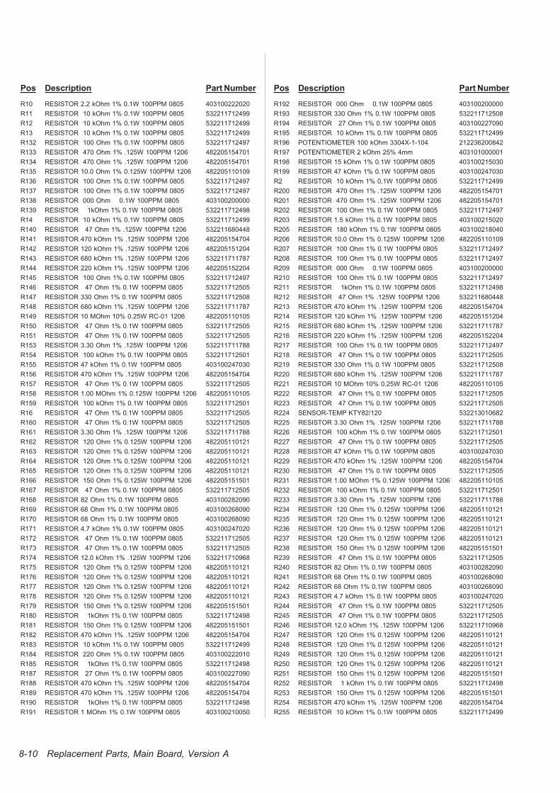
Pos Description Part Number
R10 RESISTOR 2.2 kOhm 1% 0.1W 100PPM 0805 403100222020
R11 RESISTOR 10 kOhm 1% 0.1W 100PPM 0805 532211712499
R12 RESISTOR 10 kOhm 1% 0.1W 100PPM 0805 532211712499
R13 RESISTOR 10 kOhm 1% 0.1W 100PPM 0805 532211712499
R132 RESISTOR 100 Ohm 1% 0.1W 100PPM 0805 532211712497
R133 RESISTOR 470 Ohm 1% .125W 100PPM 1206 482205154701
R134 RESISTOR 470 Ohm 1% .125W 100PPM 1206 482205154701
R135 RESISTOR 10.0 Ohm 1% 0.125W 100PPM 1206 482205110109
R136 RESISTOR 100 Ohm 1% 0.1W 100PPM 0805 532211712497
R137 RESISTOR 100 Ohm 1% 0.1W 100PPM 0805 532211712497
R138 RESISTOR 000 Ohm 0.1W 100PPM 0805 403100200000
R139 RESISTOR 1kOhm 1% 0.1W 100PPM 0805 532211712498
R14 RESISTOR 10 kOhm 1% 0.1W 100PPM 0805 532211712499
R140 RESISTOR 47 Ohm 1% .125W 100PPM 1206 532211680448
R141 RESISTOR 470 kOhm 1% .125W 100PPM 1206 482205154704
R142 RESISTOR 120 kOhm 1% .125W 100PPM 1206 482205151204
R143 RESISTOR 680 kOhm 1% .125W 100PPM 1206 532211711787
R144 RESISTOR 220 kOhm 1% .125W 100PPM 1206 482205152204
R145 RESISTOR 100 Ohm 1% 0.1W 100PPM 0805 532211712497
R146 RESISTOR 47 Ohm 1% 0.1W 100PPM 0805 532211712505
R147 RESISTOR 330 Ohm 1% 0.1W 100PPM 0805 532211712508
R148 RESISTOR 680 kOhm 1% .125W 100PPM 1206 532211711787
R149 RESISTOR 10 MOhm 10% 0.25W RC-01 1206 482205110105
R150 RESISTOR 47 Ohm 1% 0.1W 100PPM 0805 532211712505
R151 RESISTOR 47 Ohm 1% 0.1W 100PPM 0805 532211712505
R153 RESISTOR 3.30 Ohm 1% .125W 100PPM 1206 532211711788
R154 RESISTOR 100 kOhm 1% 0.1W 100PPM 0805 532211712501
R155 RESISTOR 47 kOhm 1% 0.1W 100PPM 0805 403100247030
R156 RESISTOR 470 kOhm 1% .125W 100PPM 1206 482205154704
R157 RESISTOR 47 Ohm 1% 0.1W 100PPM 0805 532211712505
R158 RESISTOR 1.00 MOhm 1% 0.125W 100PPM 1206 482205110105
R159 RESISTOR 100 kOhm 1% 0.1W 100PPM 0805 532211712501
R16 RESISTOR 47 Ohm 1% 0.1W 100PPM 0805 532211712505
R160 RESISTOR 47 Ohm 1% 0.1W 100PPM 0805 532211712505
R161 RESISTOR 3.30 Ohm 1% .125W 100PPM 1206 532211711788
R162 RESISTOR 120 Ohm 1% 0.125W 100PPM 1206 482205110121
R163 RESISTOR 120 Ohm 1% 0.125W 100PPM 1206 482205110121
R164 RESISTOR 120 Ohm 1% 0.125W 100PPM 1206 482205110121
R165 RESISTOR 120 Ohm 1% 0.125W 100PPM 1206 482205110121
R166 RESISTOR 150 Ohm 1% 0.125W 100PPM 1206 482205151501
R167 RESISTOR 47 Ohm 1% 0.1W 100PPM 0805 532211712505
R168 RESISTOR 82 Ohm 1% 0.1W 100PPM 0805 403100282090
R169 RESISTOR 68 Ohm 1% 0.1W 100PPM 0805 403100268090
R170 RESISTOR 68 Ohm 1% 0.1W 100PPM 0805 403100268090
R171 RESISTOR 4.7 kOhm 1% 0.1W 100PPM 0805 403100247020
R172 RESISTOR 47 Ohm 1% 0.1W 100PPM 0805 532211712505
R173 RESISTOR 47 Ohm 1% 0.1W 100PPM 0805 532211712505
R174 RESISTOR 12.0 kOhm 1% .125W 100PPM 1206 532211710968
R175 RESISTOR 120 Ohm 1% 0.125W 100PPM 1206 482205110121
R176 RESISTOR 120 Ohm 1% 0.125W 100PPM 1206 482205110121
R177 RESISTOR 120 Ohm 1% 0.125W 100PPM 1206 482205110121
R178 RESISTOR 120 Ohm 1% 0.125W 100PPM 1206 482205110121
R179 RESISTOR 150 Ohm 1% 0.125W 100PPM 1206 482205151501
R180 RESISTOR 1kOhm 1% 0.1W 100PPM 0805 532211712498
R181 RESISTOR 150 Ohm 1% 0.125W 100PPM 1206 482205151501
R182 RESISTOR 470 kOhm 1% .125W 100PPM 1206 482205154704
R183 RESISTOR 10 kOhm 1% 0.1W 100PPM 0805 532211712499
R184 RESISTOR 220 Ohm 1% 0.1W 100PPM 0805 403100222010
R185 RESISTOR 1kOhm 1% 0.1W 100PPM 0805 532211712498
R187 RESISTOR 27 Ohm 1% 0.1W 100PPM 0805 403100227090
R188 RESISTOR 470 kOhm 1% .125W 100PPM 1206 482205154704
R189 RESISTOR 470 kOhm 1% .125W 100PPM 1206 482205154704
R190 RESISTOR 1kOhm 1% 0.1W 100PPM 0805 532211712498
R191 RESISTOR 1 MOhm 1% 0.1W 100PPM 0805 403100210050
Pos Description Part Number
R192 RESISTOR 000 Ohm 0.1W 100PPM 0805 403100200000
R193 RESISTOR 330 Ohm 1% 0.1W 100PPM 0805 532211712508
R194 RESISTOR 27 Ohm 1% 0.1W 100PPM 0805 403100227090
R195 RESISTOR 10 kOhm 1% 0.1W 100PPM 0805 532211712499
R196 POTENTIOMETER 100 kOhm 3304X-1-104 212236200842
R197 POTENTIOMETER 2 kOhm 25% 4mm 403101000001
R198 RESISTOR 15 kOhm 1% 0.1W 100PPM 0805 403100215030
R199 RESISTOR 47 kOhm 1% 0.1W 100PPM 0805 403100247030
R2 RESISTOR 10 kOhm 1% 0.1W 100PPM 0805 532211712499
R200 RESISTOR 470 Ohm 1% .125W 100PPM 1206 482205154701
R201 RESISTOR 470 Ohm 1% .125W 100PPM 1206 482205154701
R202 RESISTOR 100 Ohm 1% 0.1W 100PPM 0805 532211712497
R203 RESISTOR 1.5 kOhm 1% 0.1W 100PPM 0805 403100215020
R205 RESISTOR 180 kOhm 1% 0.1W 100PPM 0805 403100218040
R206 RESISTOR 10.0 Ohm 1% 0.125W 100PPM 1206 482205110109
R207 RESISTOR 100 Ohm 1% 0.1W 100PPM 0805 532211712497
R208 RESISTOR 100 Ohm 1% 0.1W 100PPM 0805 532211712497
R209 RESISTOR 000 Ohm 0.1W 100PPM 0805 403100200000
R210 RESISTOR 100 Ohm 1% 0.1W 100PPM 0805 532211712497
R211 RESISTOR 1kOhm 1% 0.1W 100PPM 0805 532211712498
R212 RESISTOR 47 Ohm 1% .125W 100PPM 1206 532211680448
R213 RESISTOR 470 kOhm 1% .125W 100PPM 1206 482205154704
R214 RESISTOR 120 kOhm 1% .125W 100PPM 1206 482205151204
R215 RESISTOR 680 kOhm 1% .125W 100PPM 1206 532211711787
R216 RESISTOR 220 kOhm 1% .125W 100PPM 1206 482205152204
R217 RESISTOR 100 Ohm 1% 0.1W 100PPM 0805 532211712497
R218 RESISTOR 47 Ohm 1% 0.1W 100PPM 0805 532211712505
R219 RESISTOR 330 Ohm 1% 0.1W 100PPM 0805 532211712508
R220 RESISTOR 680 kOhm 1% .125W 100PPM 1206 532211711787
R221 RESISTOR 10 MOhm 10% 0.25W RC-01 1206 482205110105
R222 RESISTOR 47 Ohm 1% 0.1W 100PPM 0805 532211712505
R223 RESISTOR 47 Ohm 1% 0.1W 100PPM 0805 532211712505
R224 SENSOR-TEMP KTY82/120 532213010682
R225 RESISTOR 3.30 Ohm 1% .125W 100PPM 1206 532211711788
R226 RESISTOR 100 kOhm 1% 0.1W 100PPM 0805 532211712501
R227 RESISTOR 47 Ohm 1% 0.1W 100PPM 0805 532211712505
R228 RESISTOR 47 kOhm 1% 0.1W 100PPM 0805 403100247030
R229 RESISTOR 470 kOhm 1% .125W 100PPM 1206 482205154704
R230 RESISTOR 47 Ohm 1% 0.1W 100PPM 0805 532211712505
R231 RESISTOR 1.00 MOhm 1% 0.125W 100PPM 1206 482205110105
R232 RESISTOR 100 kOhm 1% 0.1W 100PPM 0805 532211712501
R233 RESISTOR 3.30 Ohm 1% .125W 100PPM 1206 532211711788
R234 RESISTOR 120 Ohm 1% 0.125W 100PPM 1206 482205110121
R235 RESISTOR 120 Ohm 1% 0.125W 100PPM 1206 482205110121
R236 RESISTOR 120 Ohm 1% 0.125W 100PPM 1206 482205110121
R237 RESISTOR 120 Ohm 1% 0.125W 100PPM 1206 482205110121
R238 RESISTOR 150 Ohm 1% 0.125W 100PPM 1206 482205151501
R239 RESISTOR 47 Ohm 1% 0.1W 100PPM 0805 532211712505
R240 RESISTOR 82 Ohm 1% 0.1W 100PPM 0805 403100282090
R241 RESISTOR 68 Ohm 1% 0.1W 100PPM 0805 403100268090
R242 RESISTOR 68 Ohm 1% 0.1W 100PPM 0805 403100268090
R243 RESISTOR 4.7 kOhm 1% 0.1W 100PPM 0805 403100247020
R244 RESISTOR 47 Ohm 1% 0.1W 100PPM 0805 532211712505
R245 RESISTOR 47 Ohm 1% 0.1W 100PPM 0805 532211712505
R246 RESISTOR 12.0 kOhm 1% .125W 100PPM 1206 532211710968
R247 RESISTOR 120 Ohm 1% 0.125W 100PPM 1206 482205110121
R248 RESISTOR 120 Ohm 1% 0.125W 100PPM 1206 482205110121
R249 RESISTOR 120 Ohm 1% 0.125W 100PPM 1206 482205110121
R250 RESISTOR 120 Ohm 1% 0.125W 100PPM 1206 482205110121
R251 RESISTOR 150 Ohm 1% 0.125W 100PPM 1206 482205151501
R252 RESISTOR 1 kOhm 1% 0.1W 100PPM 0805 532211712498
R253 RESISTOR 150 Ohm 1% 0.125W 100PPM 1206 482205151501
R254 RESISTOR 470 kOhm 1% .125W 100PPM 1206 482205154704
R255 RESISTOR 10 kOhm 1% 0.1W 100PPM 0805 532211712499
8-10 Replacement Parts, Main Board, Version A
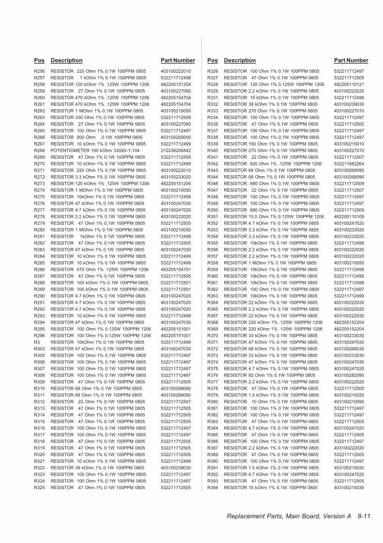
Pos Description Part Number
R256 RESISTOR 220 Ohm 1% 0.1W 100PPM 0805 403100222010
R257 RESISTOR 1 kOhm 1% 0.1W 100PPM 0805 532211712498
R258 RESISTOR 120 kOhm 1% .125W 100PPM 1206 482205151204
R259 RESISTOR 27 Ohm 1% 0.1W 100PPM 0805 403100227090
R260 RESISTOR 470 kOhm 1% .125W 100PPM 1206 482205154704
R261 RESISTOR 470 kOhm 1% .125W 100PPM 1206 482205154704
R262 RESISTOR 1 MOhm 1% 0.1W 100PPM 0805 403100210050
R263 RESISTOR 330 Ohm 1% 0.1W 100PPM 0805 532211712508
R264 RESISTOR 27 Ohm 1% 0.1W 100PPM 0805 403100227090
R265 RESISTOR 100 Ohm 1% 0.1W 100PPM 0805 532211712497
R266 RESISTOR 000 Ohm 0.1W 100PPM 0805 403100200000
R267 RESISTOR 10 kOhm 1% 0.1W 100PPM 0805 532211712499
R268 POTENTIOMETER 100 kOhm 3304X-1-104 212236200842
R269 RESISTOR 47 Ohm 1% 0.1W 100PPM 0805 532211712505
R270 RESISTOR 10 kOhm 1% 0.1W 100PPM 0805 532211712499
R271 RESISTOR 220 Ohm 1% 0.1W 100PPM 0805 403100222010
R272 RESISTOR 3.3 kOhm 1% 0.1W 100PPM 0805 403100233020
R273 RESISTOR 120 kOhm 1% .125W 100PPM 1206 482205151204
R274 RESISTOR 1 MOhm 1% 0.1W 100PPM 0805 403100210050
R275 RESISTOR 10kOhm 1% 0.1W 100PPM 0805 532211712499
R276 RESISTOR 47 kOhm 1% 0.1W 100PPM 0805 403100247030
R277 RESISTOR 4.7 kOhm 1% 0.1W 100PPM 0805 403100247020
R278 RESISTOR 2.2 kOhm 1% 0.1W 100PPM 0805 403100222020
R279 RESISTOR 47 Ohm 1% 0.1W 100PPM 0805 532211712505
R280 RESISTOR 1 MOhm 1% 0.1W 100PPM 0805 403100210050
R281 RESISTOR 1kOhm 1% 0.1W 100PPM 0805 532211712498
R282 RESISTOR 47 Ohm 1% 0.1W 100PPM 0805 532211712505
R283 RESISTOR 47 kOhm 1% 0.1W 100PPM 0805 403100247030
R284 RESISTOR 10 kOhm 1% 0.1W 100PPM 0805 532211712499
R285 RESISTOR 10 kOhm 1% 0.1W 100PPM 0805 532211712499
R286 RESISTOR 470 Ohm 1% .125W 100PPM 1206 482205154701
R287 RESISTOR 47 Ohm 1% 0.1W 100PPM 0805 532211712505
R288 RESISTOR 100 kOhm 1% 0.1W 100PPM 0805 532211712501
R289 RESISTOR 100 kOhm 1% 0.1W 100PPM 0805 532211712501
R290 RESISTOR 4.7 kOhm 1% 0.1W 100PPM 0805 403100247020
R291 RESISTOR 4.7 kOhm 1% 0.1W 100PPM 0805 403100247020
R292 RESISTOR 4.7 kOhm 1% 0.1W 100PPM 0805 403100247020
R293 RESISTOR 10 kOhm 1% 0.1W 100PPM 0805 532211712499
R294 RESISTOR 47 kOhm 1% 0.1W 100PPM 0805 403100247030
R295 RESISTOR 100 Ohm 1% 0.125W 100PPM 1206 482205151001
R296 RESISTOR 100 Ohm 1% 0.125W 100PPM 1206 482205151001
R3 RESISTOR 10kOhm 1% 0.1W 100PPM 0805 532211712499
R303 RESISTOR 47 kOhm 1% 0.1W 100PPM 0805 403100247030
R305 RESISTOR 100 Ohm 1% 0.1W 100PPM 0805 532211712497
R306 RESISTOR 100 Ohm 1% 0.1W 100PPM 0805 532211712497
R307 RESISTOR 100 Ohm 1% 0.1W 100PPM 0805 532211712497
R308 RESISTOR 100 Ohm 1% 0.1W 100PPM 0805 532211712497
R309 RESISTOR 47 Ohm 1% 0.1W 100PPM 0805 532211712505
R310 RESISTOR 68 Ohm 1% 0.1W 100PPM 0805 403100268090
R311 RESISTOR 68 Ohm 1% 0.1W 100PPM 0805 403100268090
R312 RESISTOR 22 Ohm 1% 0.1W 100PPM 0805 532211712507
R313 RESISTOR 47 Ohm 1% 0.1W 100PPM 0805 532211712505
R314 RESISTOR 47 Ohm 1% 0.1W 100PPM 0805 532211712505
R315 RESISTOR 47 Ohm 1% 0.1W 100PPM 0805 532211712505
R316 RESISTOR 100 Ohm 1% 0.1W 100PPM 0805 532211712497
R317 RESISTOR 100 Ohm 1% 0.1W 100PPM 0805 532211712497
R318 RESISTOR 47 Ohm 1% 0.1W 100PPM 0805 532211712505
R319 RESISTOR 47 Ohm 1% 0.1W 100PPM 0805 532211712505
R320 RESISTOR 47 Ohm 1% 0.1W 100PPM 0805 532211712505
R321 RESISTOR 10 kOhm 1% 0.1W 100PPM 0805 532211712499
R322 RESISTOR 39 kOhm 1% 0.1W 100PPM 0805 403100239030
R323 RESISTOR 100 Ohm 1% 0.1W 100PPM 0805 532211712497
R324 RESISTOR 100 Ohm 1% 0.1W 100PPM 0805 532211712497
R325 RESISTOR 47 Ohm 1% 0.1W 100PPM 0805 532211712505
Pos Description Part Number
R326 RESISTOR 100 Ohm 1% 0.1W 100PPM 0805 532211712497
R327 RESISTOR 47 Ohm 1% 0.1W 100PPM 0805 532211712505
R328 RESISTOR 120 Ohm 1% 0.125W 100PPM 1206 482205110121
R329 RESISTOR 2.2 kOhm 1% 0.1W 100PPM 0805 403100222020
R331 RESISTOR 10 kOhm 1% 0.1W 100PPM 0805 532211712499
R332 RESISTOR 39 kOhm 1% 0.1W 100PPM 0805 403100239030
R333 RESISTOR 270 Ohm 1% 0.1W 100PPM 0805 403100227010
R334 RESISTOR 100 Ohm 1% 0.1W 100PPM 0805 532211712497
R335 RESISTOR 47 Ohm 1% 0.1W 100PPM 0805 532211712505
R337 RESISTOR 100 Ohm 1% 0.1W 100PPM 0805 532211712497
R338 RESISTOR 100 Ohm 1% 0.1W 100PPM 0805 532211712497
R339 RESISTOR 150 Ohm 1% 0.1W 100PPM 0805 403100215010
R340 RESISTOR 270 Ohm 1% 0.1W 100PPM 0805 403100227010
R341 RESISTOR 22 Ohm 1% 0.1W 100PPM 0805 532211712507
R342 RESISTOR 820 Ohm 1% .125W 100PPM 1206 532211682264
R343 RESISTOR 68 Ohm 1% 0.1W 100PPM 0805 403100268090
R344 RESISTOR 68 Ohm 1% 0.1W 100PPM 0805 403100268090
R346 RESISTOR 680 Ohm 1% 0.1W 100PPM 0805 532211712509
R347 RESISTOR 22 Ohm 1% 0.1W 100PPM 0805 532211712507
R348 RESISTOR 100 Ohm 1% 0.1W 100PPM 0805 532211712497
R349 RESISTOR 100 Ohm 1% 0.1W 100PPM 0805 532211712497
R350 RESISTOR 680 Ohm 1% 0.1W 100PPM 0805 532211712509
R351 RESISTOR 10.0 Ohm 1% 0.125W 100PPM 1206 482205110109
R352 RESISTOR 4.7 kOhm 1% 0.1W 100PPM 0805 403100247020
R353 RESISTOR 3.3 kOhm 1% 0.1W 100PPM 0805 403100233020
R354 RESISTOR 3.3 kOhm 1% 0.1W 100PPM 0805 403100233020
R355 RESISTOR 10kOhm 1% 0.1W 100PPM 0805 532211712499
R356 RESISTOR 2.2 kOhm 1% 0.1W 100PPM 0805 403100222020
R357 RESISTOR 2.2 kOhm 1% 0.1W 100PPM 0805 403100222020
R358 RESISTOR 1 MOhm 1% 0.1W 100PPM 0805 403100210050
R359 RESISTOR 10kOhm 1% 0.1W 100PPM 0805 532211712499
R360 RESISTOR 10kOhm 1% 0.1W 100PPM 0805 532211712499
R361 RESISTOR 10kOhm 1% 0.1W 100PPM 0805 532211712499
R362 RESISTOR 100 Ohm 1% 0.1W 100PPM 0805 532211712497
R363 RESISTOR 10kOhm 1% 0.1W 100PPM 0805 532211712499
R364 RESISTOR 22 kOhm 1% 0.1W 100PPM 0805 403100222030
R365 RESISTOR 2.2 kOhm 1% 0.1W 100PPM 0805 403100222020
R367 RESISTOR 22 kOhm 1% 0.1W 100PPM 0805 403100222030
R368 RESISTOR 220 kOhm 1% .125W 100PPM 1206 482205152204
R369 RESISTOR 220 kOhm 1% .125W 100PPM 1206 482205152204
R370 RESISTOR 33 kOhm 1% 0.1W 100PPM 0805 403100233030
R371 RESISTOR 47 kOhm 1% 0.1W 100PPM 0805 403100247030
R372 RESISTOR 68 kOhm 1% 0.1W 100PPM 0805 403100268030
R373 RESISTOR 33 kOhm 1% 0.1W 100PPM 0805 403100233030
R374 RESISTOR 47 kOhm 1% 0.1W 100PPM 0805 403100247030
R375 RESISTOR 4.7 kOhm 1% 0.1W 100PPM 0805 403100247020
R376 RESISTOR 82 Ohm 1% 0.1W 100PPM 0805 403100282090
R377 RESISTOR 2.2 kOhm 1% 0.1W 100PPM 0805 403100222020
R378 RESISTOR 47 Ohm 1% 0.1W 100PPM 0805 532211712505
R379 RESISTOR 1.5 kOhm 1% 0.1W 100PPM 0805 403100215020
R380 RESISTOR 10 Ohm 1% 0.1W 100PPM 0805 403100210090
R381 RESISTOR 100 Ohm 1% 0.1W 100PPM 0805 532211712497
R382 RESISTOR 100 Ohm 1% 0.1W 100PPM 0805 532211712497
R383 RESISTOR 47 Ohm 1% 0.1W 100PPM 0805 532211712505
R384 RESISTOR 4.7 kOhm 1% 0.1W 100PPM 0805 403100247020
R385 RESISTOR 47 Ohm 1% 0.1W 100PPM 0805 532211712505
R386 RESISTOR 100 Ohm 1% 0.1W 100PPM 0805 532211712497
R387 RESISTOR 2.2 kOhm 1% 0.1W 100PPM 0805 403100222020
R389 RESISTOR 47 Ohm 1% 0.1W 100PPM 0805 532211712505
R390 RESISTOR 100 Ohm 1% 0.1W 100PPM 0805 532211712497
R391 RESISTOR 1.5 kOhm 1% 0.1W 100PPM 0805 403100215020
R392 RESISTOR 4.7 kOhm 1% 0.1W 100PPM 0805 403100247020
R393 RESISTOR 47 Ohm 1% 0.1W 100PPM 0805 532211712505
R394 RESISTOR 15 kOhm 1% 0.1W 100PPM 0805 403100215030
Replacement Parts, Main Board, Version A 8-11
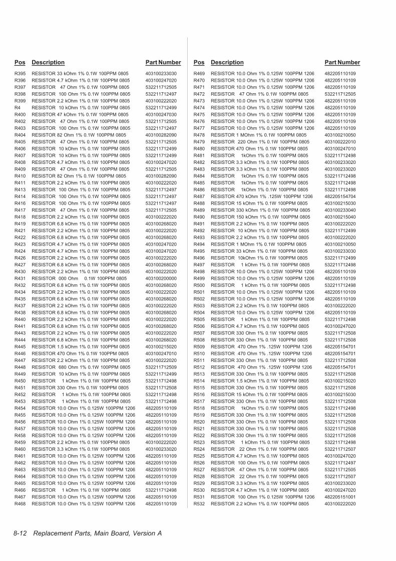
Pos Description Part Number
R395 RESISTOR 33 kOhm 1% 0.1W 100PPM 0805 403100233030
R396 RESISTOR 4.7 kOhm 1% 0.1W 100PPM 0805 403100247020
R397 RESISTOR 47 Ohm 1% 0.1W 100PPM 0805 532211712505
R398 RESISTOR 100 Ohm 1% 0.1W 100PPM 0805 532211712497
R399 RESISTOR 2.2 kOhm 1% 0.1W 100PPM 0805 403100222020
R4 RESISTOR 10 kOhm 1% 0.1W 100PPM 0805 532211712499
R400 RESISTOR 47 kOhm 1% 0.1W 100PPM 0805 403100247030
R402 RESISTOR 47 Ohm 1% 0.1W 100PPM 0805 532211712505
R403 RESISTOR 100 Ohm 1% 0.1W 100PPM 0805 532211712497
R404 RESISTOR 82 Ohm 1% 0.1W 100PPM 0805 403100282090
R405 RESISTOR 47 Ohm 1% 0.1W 100PPM 0805 532211712505
R406 RESISTOR 10 kOhm 1% 0.1W 100PPM 0805 532211712499
R407 RESISTOR 10 kOhm 1% 0.1W 100PPM 0805 532211712499
R408 RESISTOR 4.7 kOhm 1% 0.1W 100PPM 0805 403100247020
R409 RESISTOR 47 Ohm 1% 0.1W 100PPM 0805 532211712505
R410 RESISTOR 82 Ohm 1% 0.1W 100PPM 0805 403100282090
R411 RESISTOR 2.2 kOhm 1% 0.1W 100PPM 0805 403100222020
R413 RESISTOR 100 Ohm 1% 0.1W 100PPM 0805 532211712497
R414 RESISTOR 100 Ohm 1% 0.1W 100PPM 0805 532211712497
R416 RESISTOR 100 Ohm 1% 0.1W 100PPM 0805 532211712497
R417 RESISTOR 47 Ohm 1% 0.1W 100PPM 0805 532211712505
R418 RESISTOR 2.2 kOhm 1% 0.1W 100PPM 0805 403100222020
R419 RESISTOR 6.8 kOhm 1% 0.1W 100PPM 0805 403100268020
R421 RESISTOR 2.2 kOhm 1% 0.1W 100PPM 0805 403100222020
R422 RESISTOR 6.8 kOhm 1% 0.1W 100PPM 0805 403100268020
R423 RESISTOR 4.7 kOhm 1% 0.1W 100PPM 0805 403100247020
R424 RESISTOR 4.7 kOhm 1% 0.1W 100PPM 0805 403100247020
R426 RESISTOR 2.2 kOhm 1% 0.1W 100PPM 0805 403100222020
R427 RESISTOR 6.8 kOhm 1% 0.1W 100PPM 0805 403100268020
R430 RESISTOR 2.2 kOhm 1% 0.1W 100PPM 0805 403100222020
R431 RESISTOR 000 Ohm 0.1W 100PPM 0805 403100200000
R432 RESISTOR 6.8 kOhm 1% 0.1W 100PPM 0805 403100268020
R434 RESISTOR 2.2 kOhm 1% 0.1W 100PPM 0805 403100222020
R435 RESISTOR 6.8 kOhm 1% 0.1W 100PPM 0805 403100268020
R437 RESISTOR 2.2 kOhm 1% 0.1W 100PPM 0805 403100222020
R438 RESISTOR 6.8 kOhm 1% 0.1W 100PPM 0805 403100268020
R440 RESISTOR 2.2 kOhm 1% 0.1W 100PPM 0805 403100222020
R441 RESISTOR 6.8 kOhm 1% 0.1W 100PPM 0805 403100268020
R443 RESISTOR 2.2 kOhm 1% 0.1W 100PPM 0805 403100222020
R444 RESISTOR 6.8 kOhm 1% 0.1W 100PPM 0805 403100268020
R445 RESISTOR 1.5 kOhm 1% 0.1W 100PPM 0805 403100215020
R446 RESISTOR 470 Ohm 1% 0.1W 100PPM 0805 403100247010
R447 RESISTOR 2.2 kOhm 1% 0.1W 100PPM 0805 403100222020
R448 RESISTOR 680 Ohm 1% 0.1W 100PPM 0805 532211712509
R449 RESISTOR 10 kOhm 1% 0.1W 100PPM 0805 532211712499
R450 RESISTOR 1 kOhm 1% 0.1W 100PPM 0805 532211712498
R451 RESISTOR 330 Ohm 1% 0.1W 100PPM 0805 532211712508
R452 RESISTOR 1 kOhm 1% 0.1W 100PPM 0805 532211712498
R453 RESISTOR 1 kOhm 1% 0.1W 100PPM 0805 532211712498
R454 RESISTOR 10.0 Ohm 1% 0.125W 100PPM 1206 482205110109
R455 RESISTOR 10.0 Ohm 1% 0.125W 100PPM 1206 482205110109
R456 RESISTOR 10.0 Ohm 1% 0.125W 100PPM 1206 482205110109
R457 RESISTOR 10.0 Ohm 1% 0.125W 100PPM 1206 482205110109
R458 RESISTOR 10.0 Ohm 1% 0.125W 100PPM 1206 482205110109
R459 RESISTOR 2.2 kOhm 1% 0.1W 100PPM 0805 403100222020
R460 RESISTOR 3.3 kOhm 1% 0.1W 100PPM 0805 403100233020
R461 RESISTOR 10.0 Ohm 1% 0.125W 100PPM 1206 482205110109
R462 RESISTOR 10.0 Ohm 1% 0.125W 100PPM 1206 482205110109
R463 RESISTOR 10.0 Ohm 1% 0.125W 100PPM 1206 482205110109
R464 RESISTOR 10.0 Ohm 1% 0.125W 100PPM 1206 482205110109
R465 RESISTOR 10.0 Ohm 1% 0.125W 100PPM 1206 482205110109
R466 RESISTOR 1 kOhm 1% 0.1W 100PPM 0805 532211712498
R467 RESISTOR 10.0 Ohm 1% 0.125W 100PPM 1206 482205110109
R468 RESISTOR 10.0 Ohm 1% 0.125W 100PPM 1206 482205110109
Pos Description Part Number
R469 RESISTOR 10.0 Ohm 1% 0.125W 100PPM 1206 482205110109
R470 RESISTOR 10.0 Ohm 1% 0.125W 100PPM 1206 482205110109
R471 RESISTOR 10.0 Ohm 1% 0.125W 100PPM 1206 482205110109
R472 RESISTOR 47 Ohm 1% 0.1W 100PPM 0805 532211712505
R473 RESISTOR 10.0 Ohm 1% 0.125W 100PPM 1206 482205110109
R474 RESISTOR 10.0 Ohm 1% 0.125W 100PPM 1206 482205110109
R475 RESISTOR 10.0 Ohm 1% 0.125W 100PPM 1206 482205110109
R476 RESISTOR 10.0 Ohm 1% 0.125W 100PPM 1206 482205110109
R477 RESISTOR 10.0 Ohm 1% 0.125W 100PPM 1206 482205110109
R478 RESISTOR 1 MOhm 1% 0.1W 100PPM 0805 403100210050
R479 RESISTOR 220 Ohm 1% 0.1W 100PPM 0805 403100222010
R480 RESISTOR 470 Ohm 1% 0.1W 100PPM 0805 403100247010
R481 RESISTOR 1kOhm 1% 0.1W 100PPM 0805 532211712498
R482 RESISTOR 3.3 kOhm 1% 0.1W 100PPM 0805 403100233020
R483 RESISTOR 3.3 kOhm 1% 0.1W 100PPM 0805 403100233020
R484 RESISTOR 1kOhm 1% 0.1W 100PPM 0805 532211712498
R485 RESISTOR 1kOhm 1% 0.1W 100PPM 0805 532211712498
R486 RESISTOR 1kOhm 1% 0.1W 100PPM 0805 532211712498
R487 RESISTOR 470 kOhm 1% .125W 100PPM 1206 482205154704
R488 RESISTOR 15 kOhm 1% 0.1W 100PPM 0805 403100215030
R489 RESISTOR 330 kOhm 1% 0.1W 100PPM 0805 403100233040
R490 RESISTOR 150 kOhm 1% 0.1W 100PPM 0805 403100215040
R491 RESISTOR 2.2 kOhm 1% 0.1W 100PPM 0805 403100222020
R492 RESISTOR 10 kOhm 1% 0.1W 100PPM 0805 532211712499
R493 RESISTOR 2.2 kOhm 1% 0.1W 100PPM 0805 403100222020
R494 RESISTOR 1 MOhm 1% 0.1W 100PPM 0805 403100210050
R495 RESISTOR 33 kOhm 1% 0.1W 100PPM 0805 403100233030
R496 RESISTOR 10kOhm 1% 0.1W 100PPM 0805 532211712499
R497 RESISTOR 1 kOhm 1% 0.1W 100PPM 0805 532211712498
R498 RESISTOR 10.0 Ohm 1% 0.125W 100PPM 1206 482205110109
R499 RESISTOR 10.0 Ohm 1% 0.125W 100PPM 1206 482205110109
R500 RESISTOR 1 kOhm 1% 0.1W 100PPM 0805 532211712498
R501 RESISTOR 10.0 Ohm 1% 0.125W 100PPM 1206 482205110109
R502 RESISTOR 10.0 Ohm 1% 0.125W 100PPM 1206 482205110109
R503 RESISTOR 2.2 kOhm 1% 0.1W 100PPM 0805 403100222020
R504 RESISTOR 10.0 Ohm 1% 0.125W 100PPM 1206 482205110109
R505 RESISTOR 1 kOhm 1% 0.1W 100PPM 0805 532211712498
R506 RESISTOR 4.7 kOhm 1% 0.1W 100PPM 0805 403100247020
R507 RESISTOR 330 Ohm 1% 0.1W 100PPM 0805 532211712508
R508 RESISTOR 330 Ohm 1% 0.1W 100PPM 0805 532211712508
R509 RESISTOR 470 Ohm 1% .125W 100PPM 1206 482205154701
R510 RESISTOR 470 Ohm 1% .125W 100PPM 1206 482205154701
R511 RESISTOR 330 Ohm 1% 0.1W 100PPM 0805 532211712508
R512 RESISTOR 470 Ohm 1% .125W 100PPM 1206 482205154701
R513 RESISTOR 330 Ohm 1% 0.1W 100PPM 0805 532211712508
R514 RESISTOR 1.5 kOhm 1% 0.1W 100PPM 0805 403100215020
R515 RESISTOR 330 Ohm 1% 0.1W 100PPM 0805 532211712508
R516 RESISTOR 15 kOhm 1% 0.1W 100PPM 0805 403100215030
R517 RESISTOR 330 Ohm 1% 0.1W 100PPM 0805 532211712508
R518 RESISTOR 1kOhm 1% 0.1W 100PPM 0805 532211712498
R519 RESISTOR 330 Ohm 1% 0.1W 100PPM 0805 532211712508
R520 RESISTOR 330 Ohm 1% 0.1W 100PPM 0805 532211712508
R521 RESISTOR 330 Ohm 1% 0.1W 100PPM 0805 532211712508
R522 RESISTOR 330 Ohm 1% 0.1W 100PPM 0805 532211712508
R523 RESISTOR 1 kOhm 1% 0.1W 100PPM 0805 532211712498
R524 RESISTOR 22 Ohm 1% 0.1W 100PPM 0805 532211712507
R525 RESISTOR 4.7 kOhm 1% 0.1W 100PPM 0805 403100247020
R526 RESISTOR 100 Ohm 1% 0.1W 100PPM 0805 532211712497
R527 RESISTOR 47 Ohm 1% 0.1W 100PPM 0805 532211712505
R528 RESISTOR 22 Ohm 1% 0.1W 100PPM 0805 532211712507
R529 RESISTOR 3.3 kOhm 1% 0.1W 100PPM 0805 403100233020
R530 RESISTOR 4.7 kOhm 1% 0.1W 100PPM 0805 403100247020
R531 RESISTOR 100 Ohm 1% 0.125W 100PPM 1206 482205151001
R532 RESISTOR 2.2 kOhm 1% 0.1W 100PPM 0805 403100222020
8-12 Replacement Parts, Main Board, Version A
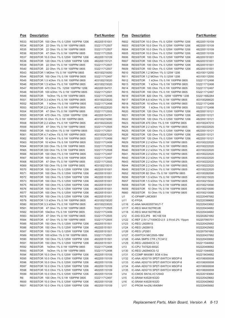
Pos Description Part Number
R533 RESISTOR 100 Ohm 1% 0.125W 100PPM 1206 482205151001
R534 RESISTOR 22 Ohm 1% 0.1W 100PPM 0805 532211712507
R535 RESISTOR 22 Ohm 1% 0.1W 100PPM 0805 532211712507
R536 RESISTOR 47 Ohm 1% 0.1W 100PPM 0805 532211712505
R537 RESISTOR 10.0 Ohm 1% 0.125W 100PPM 1206 482205110109
R538 RESISTOR 120 Ohm 1% 0.125W 100PPM 1206 482205110121
R539 RESISTOR 22 Ohm 1% 0.1W 100PPM 0805 532211712507
R540 RESISTOR 22 Ohm 1% 0.1W 100PPM 0805 532211712507
R543 RESISTOR 1 MOhm 1% 0.1W 100PPM 0805 403100210050
R544 RESISTOR 100 Ohm 1% 0.1W 100PPM 0805 532211712497
R545 RESISTOR 1.5 kOhm 1% 0.1W 100PPM 0805 403100215020
R546 RESISTOR 1.5 kOhm 1% 0.1W 100PPM 0805 403100215020
R547 RESISTOR 470 Ohm 1% .125W 100PPM 1206 482205154701
R548 RESISTOR 100 kOhm 1% 0.1W 100PPM 0805 532211712501
R549 RESISTOR 1kOhm 1% 0.1W 100PPM 0805 532211712498
R551 RESISTOR 3.3 kOhm 1% 0.1W 100PPM 0805 403100233020
R552 RESISTOR 1 kOhm 1% 0.1W 100PPM 0805 532211712498
R553 RESISTOR 2.2 kOhm 1% 0.1W 100PPM 0805 403100222020
R554 RESISTOR 47 Ohm 1% 0.1W 100PPM 0805 532211712505
R555 RESISTOR 470 Ohm 1% .125W 100PPM 1206 482205154701
R557 RESISTOR 15 Ohm 1% 0.1W 100PPM 0805 403100215090
R558 RESISTOR 2.2 kOhm 1% 0.1W 100PPM 0805 403100222020
R559 RESISTOR 47 Ohm 1% 0.1W 100PPM 0805 532211712505
R560 RESISTOR 100 kOhm 1% 0.1W 100PPM 0805 532211712501
R561 RESISTOR 4.7 kOhm 1% 0.1W 100PPM 0805 403100247020
R562 RESISTOR 10 kOhm 1% 0.1W 100PPM 0805 532211712499
R563 RESISTOR 10 kOhm 1% 0.1W 100PPM 0805 532211712499
R564 RESISTOR 330 Ohm 1% 0.1W 100PPM 0805 532211712508
R565 RESISTOR 330 Ohm 1% 0.1W 100PPM 0805 532211712508
R566 RESISTOR 100 Ohm 1% 0.1W 100PPM 0805 532211712497
R567 RESISTOR 100 Ohm 1% 0.1W 100PPM 0805 532211712497
R568 RESISTOR 47 Ohm 1% 0.1W 100PPM 0805 532211712505
R569 RESISTOR 150 Ohm 1% 0.1W 100PPM 0805 403100215010
R570 RESISTOR 100 Ohm 1% 0.125W 100PPM 1206 482205151001
R571 RESISTOR 100 Ohm 1% 0.125W 100PPM 1206 482205151001
R572 RESISTOR 100 Ohm 1% 0.125W 100PPM 1206 482205151001
R573 RESISTOR 100 Ohm 1% 0.125W 100PPM 1206 482205151001
R575 RESISTOR 100 Ohm 1% 0.125W 100PPM 1206 482205151001
R576 RESISTOR 100 Ohm 1% 0.125W 100PPM 1206 482205151001
R577 RESISTOR 100 Ohm 1% 0.125W 100PPM 1206 482205151001
R578 RESISTOR 100 Ohm 1% 0.125W 100PPM 1206 482205151001
R579 RESISTOR 1.5 kOhm 1% 0.1W 100PPM 0805 403100215020
R580 RESISTOR 3.3 kOhm 1% 0.1W 100PPM 0805 403100233020
R581 RESISTOR 47 Ohm 1% 0.1W 100PPM 0805 532211712505
R582 RESISTOR 10kOhm 1% 0.1W 100PPM 0805 532211712499
R583 RESISTOR 47 Ohm 1% 0.1W 100PPM 0805 532211712505
R584 RESISTOR 47 Ohm 1% 0.1W 100PPM 0805 532211712505
R585 RESISTOR 150 Ohm 1% 0.125W 100PPM 1206 482205151501
R586 RESISTOR 150 Ohm 1% 0.125W 100PPM 1206 482205151501
R587 RESISTOR 150 Ohm 1% 0.125W 100PPM 1206 482205151501
R589 RESISTOR 100 kOhm 1% 0.1W 100PPM 0805 532211712501
R590 RESISTOR 150 Ohm 1% 0.125W 100PPM 1206 482205151501
R591 RESISTOR 150 Ohm 1% 0.125W 100PPM 1206 482205151501
R592 RESISTOR 1kOhm 1% 0.1W 100PPM 0805 532211712498
R593 RESISTOR 1kOhm 1% 0.1W 100PPM 0805 532211712498
R594 RESISTOR 10.0 Ohm 1% 0.125W 100PPM 1206 482205110109
R595 RESISTOR 10.0 Ohm 1% 0.125W 100PPM 1206 482205110109
R596 RESISTOR 10.0 Ohm 1% 0.125W 100PPM 1206 482205110109
R597 RESISTOR 10.0 Ohm 1% 0.125W 100PPM 1206 482205110109
R598 RESISTOR 10.0 Ohm 1% 0.125W 100PPM 1206 482205110109
R599 RESISTOR 10.0 Ohm 1% 0.125W 100PPM 1206 482205110109
R6 RESISTOR 100 Ohm 1% 0.1W 100PPM 0805 532211712497
R600 RESISTOR 10.0 Ohm 1% 0.125W 100PPM 1206 482205110109
R601 RESISTOR 10.0 Ohm 1% 0.125W 100PPM 1206 482205110109
Pos Description Part Number
R602 RESISTOR 10.0 Ohm 1% 0.125W 100PPM 1206 482205110109
R603 RESISTOR 10.0 Ohm 1% 0.125W 100PPM 1206 482205110109
R604 RESISTOR 10.0 Ohm 1% 0.125W 100PPM 1206 482205110109
R605 RESISTOR 10.0 Ohm 1% 0.125W 100PPM 1206 482205110109
R606 RESISTOR 100 Ohm 1% 0.125W 100PPM 1206 482205151001
R607 RESISTOR 100 Ohm 1% 0.125W 100PPM 1206 482205151001
R608 RESISTOR 100 Ohm 1% 0.125W 100PPM 1206 482205151001
R609 RESISTOR 100 Ohm 1% 0.125W 100PPM 1206 482205151001
R610 RESISTOR 1.2 MOhm 1% 0.125W 1206 403100112050
R611 RESISTOR 1.2 MOhm 1% 0.125W 1206 403100112050
R612 RESISTOR 1 kOhm 1% 0.1W 100PPM 0805 532211712498
R613 RESISTOR 1 kOhm 1% 0.1W 100PPM 0805 532211712498
R614 RESISTOR 100 Ohm 1% 0.1W 100PPM 0805 532211712497
R615 RESISTOR 100 Ohm 1% 0.1W 100PPM 0805 532211712497
R616 RESISTOR 820 Ohm 1% .125W 100PPM 1206 532211682264
R617 RESISTOR 6.8 kOhm 1% 0.1W 100PPM 0805 403100268020
R618 RESISTOR 10 kOhm 1% 0.1W 100PPM 0805 532211712499
R619 RESISTOR 1 kOhm 1% 0.1W 100PPM 0805 532211712498
R620 RESISTOR 120 Ohm 1% 0.125W 100PPM 1206 482205110121
R621 RESISTOR 120 Ohm 1% 0.125W 100PPM 1206 482205110121
R622 RESISTOR 120 Ohm 1% 0.125W 100PPM 1206 482205110121
R623 RESISTOR 470 Ohm 1% 0.1W 100PPM 0805 403100247010
R624 RESISTOR 2.2 kOhm 1% 0.1W 100PPM 0805 403100222020
R625 RESISTOR 120 Ohm 1% 0.125W 100PPM 1206 482205110121
R626 RESISTOR 120 Ohm 1% 0.125W 100PPM 1206 482205110121
R627 RESISTOR 120 Ohm 1% 0.125W 100PPM 1206 482205110121
R629 RESISTOR 2.2 kOhm 1% 0.1W 100PPM 0805 403100222020
R630 RESISTOR 2.2 kOhm 1% 0.1W 100PPM 0805 403100222020
R640 RESISTOR 2.2 kOhm 1% 0.1W 100PPM 0805 403100222020
R641 RESISTOR 2.2 kOhm 1% 0.1W 100PPM 0805 403100222020
R642 RESISTOR 2.2 kOhm 1% 0.1W 100PPM 0805 403100222020
R643 RESISTOR 2.2 kOhm 1% 0.1W 100PPM 0805 403100222020
R644 RESISTOR 2.2 kOhm 1% 0.1W 100PPM 0805 403100222020
R645 RESISTOR 2.2 kOhm 1% 0.1W 100PPM 0805 403100222020
R652 RESISTOR 82 Ohm 1% 0.1W 100PPM 0805 403100282090
R656 RESISTOR 1.5 kOhm 1% 0.1W 100PPM 0805 403100215020
R657 RESISTOR 1.5 kOhm 1% 0.1W 100PPM 0805 403100215020
R658 RESISTOR 10 Ohm 1% 0.1W 100PPM 0805 403100210090
R659 RESISTOR 10 Ohm 1% 0.1W 100PPM 0805 403100210090
R660 RESISTOR 10 Ohm 1% 0.1W 100PPM 0805 403100210090
U1 IC-OPAMP LMC6081 932220497682
U11 IC-FPGA 932220399682
U116 IC-ANA MAX6355TWUT-T 932220433682
U117 IC-REG MAX1927REUB 932220434682
U118 IC-REG MAX1927REUB 932220434682
U12 IC-DIG ECLIPS MC10E104 932202821682
U122 IC-REF 2.5V LT1009CD-2.5 2.5V±0.2% 15ppm 932207993701
U123 IC-REG LM2991S 932220425682
U124 IC-REG LM2991S 932220425682
U126 IC-REG LP2951 932207501682
U127 IC-SWITCH MIC2505-1BM 932220437682
U128 IC-ANA SMPS CTR LTC3412 932220430682
U129 IC-REG LM2940CS-12 932211044682
U13 IC-CPU TA7S20-60QC 932220406682
U130 IC-REG LM2940CS-12 932211044682
U131 IC-COMP MAX961 SO8 4.5ns 932219434682
U132 IC-ANA ADG719 SPDT-SWITCH MSOP-8 403106000008
U133 IC-ANA ADG719 SPDT-SWITCH MSOP-8 403106000008
U134 IC-ANA ADG719 SPDT-SWITCH MSOP-8 403106000008
U135 IC-ANA ADG719 SPDT-SWITCH MSOP-8 403106000008
U14 IC-CMOS SN74LVC125AD 932220193682
U15 IC-SRAM K4S281632D 932220429682
U16 IC-SRAM K4S281632D 932220429682
U17 IC-PROM Am29LV640MH 932220405682
Replacement Parts, Main Board, Version A 8-13
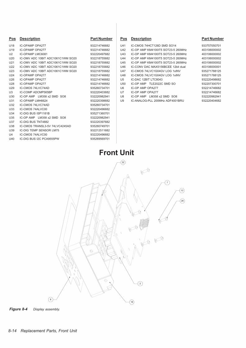
Pos Description Part Number
U18 IC-OPAMP OPA277 932214746682
U19 IC-OPAMP OPA277 932214746682
U2 IC-OPAMP LMC6081 932220497682
U20 IC-OMV ADC 10BIT ADC1061C1WM SO20 932218755682
U21 IC-OMV ADC 10BIT ADC1061C1WM SO20 932218755682
U22 IC-OMV ADC 10BIT ADC1061C1WM SO20 932218755682
U23 IC-OMV ADC 10BIT ADC1061C1WM SO20 932218755682
U24 IC-OPAMP OPA277 932214746682
U26 IC-OPAMP OPA277 932214746682
U28 IC-OPAMP OPA277 932214746682
U29 IC-CMOS 74LVC74AD 935260734701
U3 IC-COMP ADCMP565BP 932220403682
U30 IC-OP AMP LM358 x2 SMD SO8 532220982941
U31 IC-OPAMP LMH6624 932220398682
U32 IC-CMOS 74LVC74AD 935260734701
U33 IC-CMOS 74ALVC00 932220496682
U34 IC-DIG BUS ISP1181B 935271360701
U35 IC-OP AMP LM358 x2 SMD SO8 532220982941
U37 IC-DIG BUS TNT4882 932220397682
U38 IC-CMOS TRANSL3-5V 74LVC4245AD 935260749701
U39 IC-DIG TEMP SENSOR LM75 932212511682
U4 IC-CMOS 74ALVC00 932220496682
U40 IC-DIG BUS I2C PCA9555PW 935269569701
Pos Description Part Number
U41 IC-CMOS 74HCT126D SMD SO14 933757050701
U42 IC-OP AMP KM4100IT5 SOT23-5 260MHz 403106000002
U43 IC-OP AMP KM4100IT5 SOT23-5 260MHz 403106000002
U44 IC-OP AMP KM4100IT5 SOT23-5 260MHz 403106000002
U45 IC-OP AMP KM4100IT5 SOT23-5 260MHz 403106000002
U46 IC-CONV DAC MAX5156BCEE 12bit dual 403106000001
U47 IC-CMOS 74LVC1G04GV LOG 1xINV 935271788125
U48 IC-CMOS 74LVC1G04GV LOG 1xINV 935271788125
U5 IC-DAC 12BIT LTC8043 932220498682
U50 IC-OP AMP TLE2022C SMD SO 932207300701
U6 IC-OP AMP OPA277 932214746682
U7 IC-OP AMP OPA277 932214746682
U8 IC-OP AMP LM358 x2 SMD SO8 532220982941
U9 IC-ANALOG-PLL 200MHz ADF4001BRU 932220404682
8-14 Replacement Parts, Front Unit
26
7
2
188
32
13
Figure 8-4 Display assembly.
Front Unit
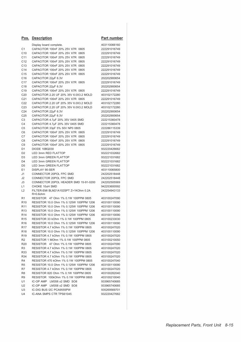
Pos. Description Part number
Display board complete. 403110066160
C1 CAPACITOR 100nF 20% 25V X7R 0805 222291016749
C10 CAPACITOR 100nF 20% 25V X7R 0805 222291016749
C11 CAPACITOR 100nF 20% 25V X7R 0805 222291016749
C12 CAPACITOR 100nF 20% 25V X7R 0805 222291016749
C13 CAPACITOR 100nF 20% 25V X7R 0805 222291016749
C14 CAPACITOR 100nF 20% 25V X7R 0805 222291016749
C15 CAPACITOR 100nF 20% 25V X7R 0805 222291016749
C16 CAPACITOR 22µF 6.3V 202202900654
C17 CAPACITOR 100nF 20% 25V X7R 0805 222291016749
C18 CAPACITOR 22µF 6.3V 202202900654
C19 CAPACITOR 100nF 20% 25V X7R 0805 222291016749
C20 CAPACITOR 2.20 UF 20% 35V 6.0X3.2 MOLD 403102172280
C21 CAPACITOR 100nF 20% 25V X7R 0805 222291016749
C22 CAPACITOR 2.20 UF 20% 35V 6.0X3.2 MOLD 403102172280
C23 CAPACITOR 2.20 UF 20% 35V 6.0X3.2 MOLD 403102172280
C24 CAPACITOR 22µF 6.3V 202202900654
C25 CAPACITOR 22µF 6.3V 202202900654
C3 CAPACITOR 4.7µF 20% 35V 0405 SMD 222215360478
C4 CAPACITOR 4.7µF 20% 35V 0405 SMD 222215360478
C5 CAPACITOR 33pF 5% 50V NP0 0805 222286115339
C6 CAPACITOR 100nF 20% 25V X7R 0805 222291016749
C7 CAPACITOR 100nF 20% 25V X7R 0805 222291016749
C8 CAPACITOR 100nF 20% 25V X7R 0805 222291016749
C9 CAPACITOR 100nF 20% 25V X7R 0805 222291016749
D1 DIODE 10BQ030 932220426682
D2 LED 3mm RED FLATTOP 932221032682
D3 LED 3mm GREEN FLATTOP 932221031682
D4 LED 3mm GREEN FLATTOP 932221031682
D5 LED 3mm GREEN FLATTOP 932221031682
E1 DISPLAY 90-SER 403110065800
J1 CONNECTOR 20POL FPC SMD 242202518448
J2 CONNECTOR 20POL FPC SMD 242202518448
J3 CONNECTOR 20POL HEADER SMD 15-91-0200 242202505569
L1 CHOKE 10uH SMD 942253600592
L2 FILTER-EMI BLM21A102SPT Z=1KOhm 0.2A
R=0.6ohm
242254943133
R1 RESISTOR 47 Ohm 1% 0.1W 100PPM 0805 403100247090
R10 RESISTOR 10.0 Ohm 1% 0.125W 100PPM 1206 403100110090
R11 RESISTOR 10.0 Ohm 1% 0.125W 100PPM 1206 403100110090
R13 RESISTOR 10.0 Ohm 1% 0.125W 100PPM 1206 403100110090
R14 RESISTOR 10.0 Ohm 1% 0.125W 100PPM 1206 403100110090
R15 RESISTOR 33 kOhm 1% 0.1W 100PPM 0805 403100233030
R16 RESISTOR 10.0 Ohm 1% 0.125W 100PPM 1206 403100110090
R17 RESISTOR 4.7 kOhm 1% 0.1W 100PPM 0805 403100247020
R18 RESISTOR 10.0 Ohm 1% 0.125W 100PPM 1206 403100110090
R19 RESISTOR 4.7 kOhm 1% 0.1W 100PPM 0805 403100247020
R2 RESISTOR 1 MOhm 1% 0.1W 100PPM 0805 403100210050
R20 RESISTOR 47 Ohm 1% 0.1W 100PPM 0805 403100247090
R3 RESISTOR 4.7 kOhm 1% 0.1W 100PPM 0805 403100247020
R33 RESISTOR 4.7 kOhm 1% 0.1W 100PPM 0805 403100247020
R34 RESISTOR 4.7 kOhm 1% 0.1W 100PPM 0805 403100247020
R4 RESISTOR 470 kOhm 1% 0.1W 100PPM 0805 403100247040
R5 RESISTOR 10.0 Ohm 1% 0.125W 100PPM 1206 403100110090
R7 RESISTOR 4.7 kOhm 1% 0.1W 100PPM 0805 403100247020
R8 RESISTOR 820 Ohm 1% 0.1W 100PPM 0805 403100282040
R9 RESISTOR 100kOhm 1% 0.1W 100PPM 0805 403100210040
U1 IC-OP AMP LM358 x2 SMD SO8 933965740685
U2 IC-OP AMP LM358 x2 SMD SO8 933965740685
U3 IC-DIG BUS I2C PCA9555PW 935269569701
U4 IC-ANA SMPS CTR TPS61045 932220427682
Replacement Parts, Front Unit 8-15
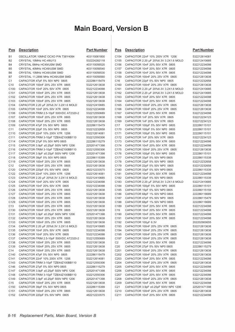
Pos Description Part Number
B1 OSCILLATOR 10MHZ OCXO P/N 738Y4084 403110061800
B2 CRYSTAL 10MHz HC-49U/13 532224282118
B4 CRYSTAL 6MHz HC49/USM SMD 403110056520
B5 CRYSTAL 40MHz HC49/USM SMD 403110056540
B6 CRYSTAL 10MHz HC49/USM SMD 403110056530
B7 CRYSTAL 11.2896 MHz HC49/USM SMD 403110056560
C1 CAPACITOR 47pF 5% 50V NP0 0805 222286115479
C10 CAPACITOR 100nF 20% 25V X7R 0805 532212613638
C100 CAPACITOR 10nF 20% 50V X7R 0805 532212234098
C101 CAPACITOR 100nF 20% 25V X7R 0805 532212613638
C102 CAPACITOR 100nF 20% 25V X7R 0805 532212613638
C103 CAPACITOR 100nF 20% 25V X7R 0805 532212613638
C104 CAPACITOR 2.20 µF 20%6.3V 3.2X1.6 MOLD 532212410685
C105 CAPACITOR 10nF 20% 50V X7R 0805 532212234098
C106 CAPACITOR-TRIM 2.5-10pF 500VDC AT2320-2 532212550689
C107 CAPACITOR 100nF 20% 25V X7R 0805 532212613638
C108 CAPACITOR 100nF 20% 25V X7R 0805 532212613638
C109 CAPACITOR 47pF 5% 50V NP0 0805 222286115479
C11 CAPACITOR 22pF 5% 50V NP0 0805 532212232658
C110 CAPACITOR 22nF 10% 200V X7R 1206 532212614081
C111 CAPACITOR-TRIM 3-10pF TZBX4Z100BB110 532212550306
C114 CAPACITOR 27pF 5% 50V NP0 0805 222286115279
C115 CAPACITOR 3.9pF ±0.25pF 500V NP0 1206 225201471398
C116 CAPACITOR-TRIM 3-10pF TZBX4Z100BB110 532212550306
C117 CAPACITOR 3.9pF ±0.25pF 500V NP0 1206 225201471398
C118 CAPACITOR 39pF 5% 50V NP0 0805 222286115399
C119 CAPACITOR 100nF 20% 25V X7R 0805 532212613638
C12 CAPACITOR 100nF 20% 25V X7R 0805 532212613638
C120 CAPACITOR 220pF 5% 50V NP0 0805 482212233575
C122 CAPACITOR 22nF 10% 200V X7R 1206 532212614081
C123 CAPACITOR 2.20 µF 20%6.3V 3.2X1.6 MOLD 532212410685
C124 CAPACITOR 10nF 20% 50V X7R 0805 532212234098
C125 CAPACITOR 10nF 20% 50V X7R 0805 532212234098
C126 CAPACITOR 100nF 20% 25V X7R 0805 532212613638
C127 CAPACITOR 100nF 20% 25V X7R 0805 532212613638
C128 CAPACITOR 100nF 20% 25V X7R 0805 532212613638
C129 CAPACITOR 100nF 20% 25V X7R 0805 532212613638
C13 CAPACITOR 100nF 20% 25V X7R 0805 532212613638
C130 CAPACITOR 100nF 20% 25V X7R 0805 532212613638
C131 CAPACITOR 3.9pF ±0.25pF 500V NP0 1206 225201471398
C132 CAPACITOR 100nF 20% 25V X7R 0805 532212613638
C133 CAPACITOR 100nF 20% 25V X7R 0805 532212613638
C134 CAPACITOR 2.20 µF 20%6.3V 3.2X1.6 MOLD 532212410685
C135 CAPACITOR 10nF 20% 50V X7R 0805 532212234098
C136 CAPACITOR 10nF 20% 50V X7R 0805 532212234098
C137 CAPACITOR-TRIM 2.5-10pF 500VDC AT2320-2 532212550689
C138 CAPACITOR 100nF 20% 25V X7R 0805 532212613638
C139 CAPACITOR 100nF 20% 25V X7R 0805 532212613638
C14 CAPACITOR 100nF 20% 25V X7R 0805 532212613638
C140 CAPACITOR 47pF 5% 50V NP0 0805 222286115479
C141 CAPACITOR 22nF 10% 200V X7R 1206 532212614081
C143 CAPACITOR-TRIM 3-10pF TZBX4Z100BB110 532212550306
C146 CAPACITOR 27pF 5% 50V NP0 0805 222286115279
C147 CAPACITOR 3.9pF ±0.25pF 500V NP0 1206 225201471398
C148 CAPACITOR-TRIM 3-10pF TZBX4Z100BB110 532212550306
C149 CAPACITOR 3.9pF ±0.25pF 500V NP0 1206 225201471398
C15 CAPACITOR 100nF 20% 25V X7R 0805 532212613638
C150 CAPACITOR 39pF 5% 50V NP0 0805 222286115399
C151 CAPACITOR 100nF 20% 25V X7R 0805 532212613638
C152 CAPACITOR 220pF 5% 50V NP0 0805 482212233575
Pos Description Part Number
C154 CAPACITOR 22nF 10% 200V X7R 1206 532212614081
C155 CAPACITOR 2.20 µF 20%6.3V 3.2X1.6 MOLD 532212410685
C156 CAPACITOR 10nF 20% 50V X7R 0805 532212234098
C157 CAPACITOR 10nF 20% 50V X7R 0805 532212234098
C158 CAPACITOR 10nF 20% 50V X7R 0805 532212234098
C159 CAPACITOR 100nF 20% 25V X7R 0805 532212613638
C16 CAPACITOR 22pF 5% 50V NP0 0805 532212232658
C160 CAPACITOR 100nF 20% 25V X7R 0805 532212613638
C161 CAPACITOR 2.20 µF 20%6.3V 3.2X1.6 MOLD 532212410685
C162 CAPACITOR 2.20 µF 20%6.3V 3.2X1.6 MOLD 532212410685
C163 CAPACITOR 10nF 20% 50V X7R 0805 532212234098
C164 CAPACITOR 10nF 20% 50V X7R 0805 532212234098
C165 CAPACITOR 100nF 20% 25V X7R 0805 532212613638
C166 CAPACITOR 100nF 20% 25V X7R 0805 532212613638
C167 CAPACITOR 10nF 20% 50V X7R 0805 532212234098
C168 CAPACITOR 1nF 20% 50V X7R 0805 532212234123
C169 CAPACITOR 1nF 20% 50V X7R 0805 532212234123
C17 CAPACITOR 100pF 5% 50V NP0 0805 222286115101
C170 CAPACITOR 100pF 5% 50V NP0 0805 222286115101
C171 CAPACITOR 100pF 5% 50V NP0 0805 222286115101
C172 CAPACITOR 1nF 20% 50V X7R 0805 532212234123
C173 CAPACITOR 10nF 20% 50V X7R 0805 532212234098
C174 CAPACITOR 10nF 20% 50V X7R 0805 532212234098
C175 CAPACITOR 100nF 20% 25V X7R 0805 532212613638
C176 CAPACITOR 100pF 5% 50V NP0 0805 222286115101
C177 CAPACITOR 33pF 5% 50V NP0 0805 222286115339
C178 CAPACITOR 22pF 5% 50V NP0 0805 532212232658
C179 CAPACITOR 22pF 5% 50V NP0 0805 532212232658
C180 CAPACITOR 33pF 5% 50V NP0 0805 222286115339
C181 CAPACITOR 10nF 20% 50V X7R 0805 532212234098
C182 CAPACITOR 33pF 5% 50V NP0 0805 222286115339
C183 CAPACITOR 2.20 µF 20%6.3V 3.2X1.6 MOLD 532212410685
C184 CAPACITOR 100pF 5% 50V NP0 0805 222286115101
C185 CAPACITOR 15pF 5% 50V NP0 0805 222286115159
C186 CAPACITOR 68pF 1% 50V NPO 0805 222286118689
C187 CAPACITOR 47pF 5% 50V NP0 0805 222286115479
C188 CAPACITOR 68pF 1% 50V NPO 0805 222286118689
C189 CAPACITOR 10nF 20% 50V X7R 0805 532212234098
C19 CAPACITOR 10nF 20% 50V X7R 0805 532212234098
C190 CAPACITOR 10nF 20% 50V X7R 0805 532212234098
C191 CAPACITOR 10nF 20% 50V X7R 0805 532212234098
C192 CAPACITOR 100µF 6.3V 202202900655
C193 CAPACITOR 100nF 20% 25V X7R 0805 532212613638
C194 CAPACITOR 100nF 20% 25V X7R 0805 532212613638
C195 CAPACITOR 100nF 20% 25V X7R 0805 532212613638
C197 CAPACITOR 100nF 20% 25V X7R 0805 532212613638
C2 CAPACITOR 10nF 20% 50V X7R 0805 532212234098
C20 CAPACITOR 27pF 5% 50V NP0 0805 222286115279
C201 CAPACITOR 100nF 20% 25V X7R 0805 532212613638
C202 CAPACITOR 100nF 20% 25V X7R 0805 532212613638
C203 CAPACITOR 10nF 20% 50V X7R 0805 532212234098
C204 CAPACITOR 100nF 20% 25V X7R 0805 532212613638
C205 CAPACITOR 10nF 20% 50V X7R 0805 532212234098
C206 CAPACITOR 10nF 20% 50V X7R 0805 532212234098
C207 CAPACITOR 10nF 20% 50V X7R 0805 532212234098
C208 CAPACITOR 100nF 20% 25V X7R 0805 532212613638
C209 CAPACITOR 10nF 20% 50V X7R 0805 532212234098
C21 CAPACITOR 3.9pF ±0.25pF 500V NP0 1206 225201471398
C210 CAPACITOR 100nF 20% 25V X7R 0805 532212613638
C211 CAPACITOR 10nF 20% 50V X7R 0805 532212234098
8-16 Replacement Parts, Main Board, Version B
Main Board, Version B
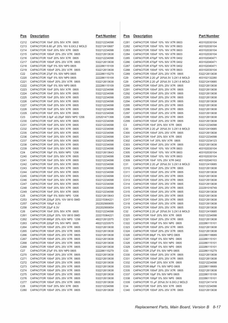
Pos Description Part Number
C212 CAPACITOR 10nF 20% 50V X7R 0805 532212234098
C213 CAPACITOR 6.80 µF 20% 16V 6.0X3.2 MOLD 532212410687
C214 CAPACITOR 10nF 20% 50V X7R 0805 532212234098
C215 CAPACITOR 100nF 20% 25V X7R 0805 532212613638
C216 CAPACITOR 10nF 20% 50V X7R 0805 532212234098
C217 CAPACITOR 100nF 20% 25V X7R 0805 532212613638
C218 CAPACITOR 10pF 5% 50V NP0 0805 222286115109
C219 CAPACITOR 100nF 20% 25V X7R 0805 532212613638
C22 CAPACITOR 27pF 5% 50V NP0 0805 222286115279
C220 CAPACITOR 10pF 5% 50V NP0 0805 222286115109
C221 CAPACITOR 100nF 20% 25V X7R 0805 532212613638
C222 CAPACITOR 10pF 5% 50V NP0 0805 222286115109
C223 CAPACITOR 10nF 20% 50V X7R 0805 532212234098
C224 CAPACITOR 10nF 20% 50V X7R 0805 532212234098
C225 CAPACITOR 10nF 20% 50V X7R 0805 532212234098
C226 CAPACITOR 10nF 20% 50V X7R 0805 532212234098
C227 CAPACITOR 10nF 20% 50V X7R 0805 532212234098
C228 CAPACITOR 10nF 20% 50V X7R 0805 532212234098
C229 CAPACITOR 10nF 20% 50V X7R 0805 532212234098
C23 CAPACITOR 3.9pF ±0.25pF 500V NP0 1206 225201471398
C230 CAPACITOR 10nF 20% 50V X7R 0805 532212234098
C231 CAPACITOR 10nF 20% 50V X7R 0805 532212234098
C232 CAPACITOR 10nF 20% 50V X7R 0805 532212234098
C235 CAPACITOR 10nF 20% 50V X7R 0805 532212234098
C236 CAPACITOR 10nF 20% 50V X7R 0805 532212234098
C237 CAPACITOR 10nF 20% 50V X7R 0805 532212234098
C238 CAPACITOR 10nF 20% 50V X7R 0805 532212234098
C239 CAPACITOR 10nF 20% 50V X7R 0805 532212234098
C24 CAPACITOR 10pF 5% 500V NP0 1206 532212613643
C240 CAPACITOR 10nF 20% 50V X7R 0805 532212234098
C241 CAPACITOR 10nF 20% 50V X7R 0805 532212234098
C242 CAPACITOR 10nF 20% 50V X7R 0805 532212234098
C243 CAPACITOR 10nF 20% 50V X7R 0805 532212234098
C244 CAPACITOR 10nF 20% 50V X7R 0805 532212234098
C245 CAPACITOR 10nF 20% 50V X7R 0805 532212234098
C246 CAPACITOR 10nF 20% 50V X7R 0805 532212234098
C247 CAPACITOR 10nF 20% 50V X7R 0805 532212234098
C248 CAPACITOR 10nF 20% 50V X7R 0805 532212234098
C249 CAPACITOR 10nF 20% 50V X7R 0805 532212234098
C25 CAPACITOR 10pF 5% 500V NP0 1206 532212613643
C253 CAPACITOR 220µF 20% 10V 0810 SMD 222215364221
C257 CAPACITOR 100µF 6.3V 202202900655
C258 CAPACITOR 22µF 6.3V 202202900654
C26 CAPACITOR 10nF 20% 50V X7R 0805 532212234098
C261 CAPACITOR 220µF 20% 10V 0810 SMD 222215364221
C262 CAPACITOR 680pF 20% 63V NP0 1206 482212612075
C263 CAPACITOR 220pF 5% 50V NP0 0805 482212233575
C264 CAPACITOR 100nF 20% 25V X7R 0805 532212613638
C265 CAPACITOR 100nF 20% 25V X7R 0805 532212613638
C266 CAPACITOR 100nF 20% 25V X7R 0805 532212613638
C267 CAPACITOR 100nF 20% 25V X7R 0805 532212613638
C268 CAPACITOR 100nF 20% 25V X7R 0805 532212613638
C269 CAPACITOR 100nF 20% 25V X7R 0805 532212613638
C27 CAPACITOR 27pF 5% 50V NP0 0805 222286115279
C270 CAPACITOR 100nF 20% 25V X7R 0805 532212613638
C271 CAPACITOR 100nF 20% 25V X7R 0805 532212613638
C272 CAPACITOR 100nF 20% 25V X7R 0805 532212613638
C273 CAPACITOR 100nF 20% 25V X7R 0805 532212613638
C274 CAPACITOR 100nF 20% 25V X7R 0805 532212613638
C275 CAPACITOR 100nF 20% 25V X7R 0805 532212613638
C276 CAPACITOR 100nF 20% 25V X7R 0805 532212613638
C277 CAPACITOR 100nF 20% 25V X7R 0805 532212613638
C28 CAPACITOR 10nF 20% 50V X7R 0805 532212234098
C280 CAPACITOR 100nF 20% 25V X7R 0805 532212613638
Pos Description Part Number
C281 CAPACITOR 100nF 10% 16V X7R 0603 403102030104
C282 CAPACITOR 100nF 10% 16V X7R 0603 403102030104
C283 CAPACITOR 100nF 10% 16V X7R 0603 403102030104
C284 CAPACITOR 100nF 10% 16V X7R 0603 403102030104
C285 CAPACITOR 470pF 10% 50V X7R 0402 403102040471
C286 CAPACITOR 470pF 10% 50V X7R 0402 403102040471
C287 CAPACITOR 470pF 10% 50V X7R 0402 403102040471
C288 CAPACITOR 100nF 10% 16V X7R 0603 403102030104
C289 CAPACITOR 100nF 20% 25V X7R 0805 532212613638
C29 CAPACITOR 2.20 µF 20%6.3V 3.2X1.6 MOLD 403102132280
C29 CAPACITOR 2.20 µF 20%6.3V 3.2X1.6 MOLD 532212410685
C290 CAPACITOR 100nF 20% 25V X7R 0805 532212613638
C291 CAPACITOR 100nF 20% 25V X7R 0805 532212613638
C292 CAPACITOR 100nF 20% 25V X7R 0805 532212613638
C293 CAPACITOR 100nF 20% 25V X7R 0805 532212613638
C294 CAPACITOR 100nF 20% 25V X7R 0805 532212613638
C295 CAPACITOR 100nF 20% 25V X7R 0805 532212613638
C296 CAPACITOR 100nF 20% 25V X7R 0805 532212613638
C297 CAPACITOR 100nF 20% 25V X7R 0805 532212613638
C298 CAPACITOR 100nF 20% 25V X7R 0805 532212613638
C299 CAPACITOR 100nF 20% 25V X7R 0805 532212613638
C3 CAPACITOR 10nF 20% 50V X7R 0805 532212234098
C30 CAPACITOR 2.20 µF 20%6.3V 3.2X1.6 MOLD 532212410685
C300 CAPACITOR 100nF 20% 25V X7R 0805 532212613638
C301 CAPACITOR 10nF 20% 50V X7R 0805 532212234098
C302 CAPACITOR 1nF 20% 50V X7R 0805 532212234123
C303 CAPACITOR 100nF 20% 25V X7R 0805 532212613638
C304 CAPACITOR 100nF 10% 16V X7R 0603 403102030104
C305 CAPACITOR 100nF 10% 16V X7R 0603 403102030104
C306 CAPACITOR 100nF 10% 16V X7R 0603 403102030104
C309 CAPACITOR 10nF 10% 25V X7R 0402 403102040103
C31 CAPACITOR 2.20 µF 20%6.3V 3.2X1.6 MOLD 532212410685
C310 CAPACITOR 100nF 20% 25V X7R 0805 532212613638
C311 CAPACITOR 100nF 20% 25V X7R 0805 532212613638
C312 CAPACITOR 100nF 20% 25V X7R 0805 532212613638
C313 CAPACITOR 100nF 20% 25V X7R 0805 532212613638
C314 CAPACITOR 100nF 20% 25V X7R 0805 532212613638
C315 CAPACITOR 100nF 20% 25V X7R 0805 222291016749
C315 CAPACITOR 100nF 20% 25V X7R 0805 532212613638
C316 CAPACITOR 100nF 20% 25V X7R 0805 532212613638
C317 CAPACITOR 100nF 20% 25V X7R 0805 532212613638
C318 CAPACITOR 100nF 20% 25V X7R 0805 532212613638
C319 CAPACITOR 100nF 20% 25V X7R 0805 532212613638
C32 CAPACITOR 2.20 µF 20%6.3V 3.2X1.6 MOLD 532212410685
C320 CAPACITOR 10nF 20% 50V X7R 0805 532212234098
C321 CAPACITOR 100nF 20% 25V X7R 0805 532212613638
C322 CAPACITOR 100pF 5% 50V NP0 0805 222286115101
C323 CAPACITOR 100nF 20% 25V X7R 0805 532212613638
C324 CAPACITOR 100nF 20% 25V X7R 0805 532212613638
C326 CAPACITOR 68pF 1% 50V NPO 0805 222286118689
C327 CAPACITOR 100pF 5% 50V NP0 0805 222286115101
C328 CAPACITOR 100pF 5% 50V NP0 0805 222286115101
C329 CAPACITOR 100pF 5% 50V NP0 0805 222286115101
C33 CAPACITOR 27pF 5% 50V NP0 0805 222286115279
C330 CAPACITOR 100nF 20% 25V X7R 0805 532212613638
C331 CAPACITOR 100nF 20% 25V X7R 0805 532212613638
C332 CAPACITOR 10nF 20% 50V X7R 0805 532212234098
C333 CAPACITOR 68pF 1% 50V NPO 0805 222286118689
C335 CAPACITOR 100nF 20% 25V X7R 0805 532212613638
C337 CAPACITOR 10pF 5% 50V NP0 0805 222286115109
C338 CAPACITOR 100pF 5% 50V NP0 0805 222286115101
C339 CAPACITOR 15 µF 20%6.3V 6.0X3.2 MOLD 532212411418
C34 CAPACITOR 10nF 20% 50V X7R 0805 532212234098
C340 CAPACITOR 100nF 20% 25V X7R 0805 532212613638
Replacement Parts, Main Board, Version B 8-17
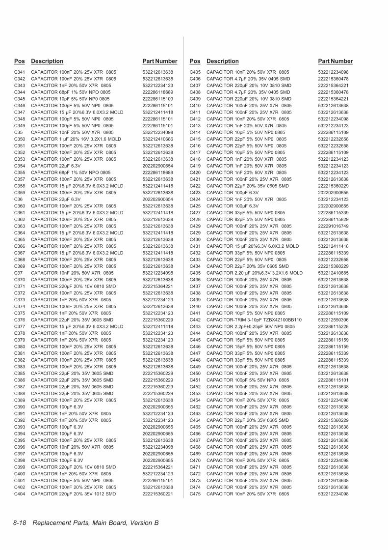
Pos Description Part Number
C341 CAPACITOR 100nF 20% 25V X7R 0805 532212613638
C342 CAPACITOR 100nF 20% 25V X7R 0805 532212613638
C343 CAPACITOR 1nF 20% 50V X7R 0805 532212234123
C344 CAPACITOR 68pF 1% 50V NPO 0805 222286118689
C345 CAPACITOR 10pF 5% 50V NP0 0805 222286115109
C346 CAPACITOR 100pF 5% 50V NP0 0805 222286115101
C347 CAPACITOR 15 µF 20%6.3V 6.0X3.2 MOLD 532212411418
C348 CAPACITOR 100pF 5% 50V NP0 0805 222286115101
C349 CAPACITOR 100pF 5% 50V NP0 0805 222286115101
C35 CAPACITOR 10nF 20% 50V X7R 0805 532212234098
C350 CAPACITOR 1 µF 20% 16V 3.2X1.6 MOLD 532212410686
C351 CAPACITOR 100nF 20% 25V X7R 0805 532212613638
C352 CAPACITOR 100nF 20% 25V X7R 0805 532212613638
C353 CAPACITOR 100nF 20% 25V X7R 0805 532212613638
C354 CAPACITOR 22µF 6.3V 202202900654
C355 CAPACITOR 68pF 1% 50V NPO 0805 222286118689
C357 CAPACITOR 100nF 20% 25V X7R 0805 532212613638
C358 CAPACITOR 15 µF 20%6.3V 6.0X3.2 MOLD 532212411418
C359 CAPACITOR 100nF 20% 25V X7R 0805 532212613638
C36 CAPACITOR 22µF 6.3V 202202900654
C360 CAPACITOR 100nF 20% 25V X7R 0805 532212613638
C361 CAPACITOR 15 µF 20%6.3V 6.0X3.2 MOLD 532212411418
C362 CAPACITOR 100nF 20% 25V X7R 0805 532212613638
C363 CAPACITOR 100nF 20% 25V X7R 0805 532212613638
C364 CAPACITOR 15 µF 20%6.3V 6.0X3.2 MOLD 532212411418
C365 CAPACITOR 100nF 20% 25V X7R 0805 532212613638
C366 CAPACITOR 100nF 20% 25V X7R 0805 532212613638
C367 CAPACITOR 15 µF 20%6.3V 6.0X3.2 MOLD 532212411418
C368 CAPACITOR 100nF 20% 25V X7R 0805 532212613638
C369 CAPACITOR 100nF 20% 25V X7R 0805 532212613638
C37 CAPACITOR 10nF 20% 50V X7R 0805 532212234098
C370 CAPACITOR 100nF 20% 25V X7R 0805 532212613638
C371 CAPACITOR 220µF 20% 10V 0810 SMD 222215364221
C372 CAPACITOR 100nF 20% 25V X7R 0805 532212613638
C373 CAPACITOR 1nF 20% 50V X7R 0805 532212234123
C374 CAPACITOR 100nF 20% 25V X7R 0805 532212613638
C375 CAPACITOR 1nF 20% 50V X7R 0805 532212234123
C376 CAPACITOR 22µF 20% 35V 0605 SMD 222215360229
C377 CAPACITOR 15 µF 20%6.3V 6.0X3.2 MOLD 532212411418
C378 CAPACITOR 1nF 20% 50V X7R 0805 532212234123
C379 CAPACITOR 1nF 20% 50V X7R 0805 532212234123
C380 CAPACITOR 100nF 20% 25V X7R 0805 532212613638
C381 CAPACITOR 100nF 20% 25V X7R 0805 532212613638
C382 CAPACITOR 100nF 20% 25V X7R 0805 532212613638
C383 CAPACITOR 100nF 20% 25V X7R 0805 532212613638
C385 CAPACITOR 22µF 20% 35V 0605 SMD 222215360229
C386 CAPACITOR 22µF 20% 35V 0605 SMD 222215360229
C387 CAPACITOR 22µF 20% 35V 0605 SMD 222215360229
C388 CAPACITOR 22µF 20% 35V 0605 SMD 222215360229
C389 CAPACITOR 100nF 20% 25V X7R 0805 532212613638
C390 CAPACITOR 100µF 6.3V 202202900655
C391 CAPACITOR 1nF 20% 50V X7R 0805 532212234123
C392 CAPACITOR 1nF 20% 50V X7R 0805 532212234123
C393 CAPACITOR 100µF 6.3V 202202900655
C394 CAPACITOR 100µF 6.3V 202202900655
C395 CAPACITOR 100nF 20% 25V X7R 0805 532212613638
C396 CAPACITOR 10nF 20% 50V X7R 0805 532212234098
C397 CAPACITOR 100µF 6.3V 202202900655
C398 CAPACITOR 100µF 6.3V 202202900655
C399 CAPACITOR 220µF 20% 10V 0810 SMD 222215364221
C400 CAPACITOR 1nF 20% 50V X7R 0805 532212234123
C401 CAPACITOR 100pF 5% 50V NP0 0805 222286115101
C402 CAPACITOR 100nF 20% 25V X7R 0805 532212613638
C404 CAPACITOR 220µF 20% 35V 1012 SMD 222215360221
Pos Description Part Number
C405 CAPACITOR 10nF 20% 50V X7R 0805 532212234098
C406 CAPACITOR 4.7µF 20% 35V 0405 SMD 222215360478
C407 CAPACITOR 220µF 20% 10V 0810 SMD 222215364221
C408 CAPACITOR 4.7µF 20% 35V 0405 SMD 222215360478
C409 CAPACITOR 220µF 20% 10V 0810 SMD 222215364221
C410 CAPACITOR 100nF 20% 25V X7R 0805 532212613638
C411 CAPACITOR 100nF 20% 25V X7R 0805 532212613638
C412 CAPACITOR 10nF 20% 50V X7R 0805 532212234098
C413 CAPACITOR 1nF 20% 50V X7R 0805 532212234123
C414 CAPACITOR 10pF 5% 50V NP0 0805 222286115109
C415 CAPACITOR 22pF 5% 50V NP0 0805 532212232658
C416 CAPACITOR 22pF 5% 50V NP0 0805 532212232658
C417 CAPACITOR 10pF 5% 50V NP0 0805 222286115109
C418 CAPACITOR 1nF 20% 50V X7R 0805 532212234123
C419 CAPACITOR 1nF 20% 50V X7R 0805 532212234123
C420 CAPACITOR 1nF 20% 50V X7R 0805 532212234123
C421 CAPACITOR 100nF 20% 25V X7R 0805 532212613638
C422 CAPACITOR 22µF 20% 35V 0605 SMD 222215360229
C423 CAPACITOR 100µF 6.3V 202202900655
C424 CAPACITOR 1nF 20% 50V X7R 0805 532212234123
C425 CAPACITOR 100µF 6.3V 202202900655
C427 CAPACITOR 33pF 5% 50V NP0 0805 222286115339
C428 CAPACITOR 82pF 5% 50V NP0 0805 222286115829
C429 CAPACITOR 100nF 20% 25V X7R 0805 222291016749
C429 CAPACITOR 100nF 20% 25V X7R 0805 532212613638
C430 CAPACITOR 100nF 20% 25V X7R 0805 532212613638
C431 CAPACITOR 15 µF 20%6.3V 6.0X3.2 MOLD 532212411418
C432 CAPACITOR 33pF 5% 50V NP0 0805 222286115339
C433 CAPACITOR 22pF 5% 50V NP0 0805 532212232658
C434 CAPACITOR 22µF 20% 35V 0605 SMD 222215360229
C435 CAPACITOR 2.20 µF 20%6.3V 3.2X1.6 MOLD 532212410685
C436 CAPACITOR 100nF 20% 25V X7R 0805 532212613638
C437 CAPACITOR 100nF 20% 25V X7R 0805 532212613638
C438 CAPACITOR 100nF 20% 25V X7R 0805 532212613638
C439 CAPACITOR 100nF 20% 25V X7R 0805 532212613638
C440 CAPACITOR 100nF 20% 25V X7R 0805 532212613638
C441 CAPACITOR 10pF 5% 50V NP0 0805 222286115109
C442 CAPACITOR-TRIM 3-10pF TZBX4Z100BB110 532212550306
C443 CAPACITOR 2.2pF±0.25pF 50V NP0 0805 222286115228
C444 CAPACITOR 100nF 20% 25V X7R 0805 532212613638
C445 CAPACITOR 15pF 5% 50V NP0 0805 222286115159
C446 CAPACITOR 15pF 5% 50V NP0 0805 222286115159
C447 CAPACITOR 33pF 5% 50V NP0 0805 222286115339
C448 CAPACITOR 33pF 5% 50V NP0 0805 222286115339
C449 CAPACITOR 100nF 20% 25V X7R 0805 532212613638
C450 CAPACITOR 100nF 20% 25V X7R 0805 532212613638
C451 CAPACITOR 100pF 5% 50V NP0 0805 222286115101
C452 CAPACITOR 100nF 20% 25V X7R 0805 532212613638
C453 CAPACITOR 100nF 20% 25V X7R 0805 532212613638
C454 CAPACITOR 10nF 20% 50V X7R 0805 532212234098
C462 CAPACITOR 100nF 20% 25V X7R 0805 532212613638
C463 CAPACITOR 100nF 20% 25V X7R 0805 532212613638
C464 CAPACITOR 22µF 20% 35V 0605 SMD 222215360229
C465 CAPACITOR 100nF 20% 25V X7R 0805 532212613638
C466 CAPACITOR 100nF 20% 25V X7R 0805 532212613638
C467 CAPACITOR 100nF 20% 25V X7R 0805 532212613638
C468 CAPACITOR 100nF 20% 25V X7R 0805 532212613638
C469 CAPACITOR 100nF 20% 25V X7R 0805 532212613638
C470 CAPACITOR 10nF 20% 50V X7R 0805 532212234098
C471 CAPACITOR 100nF 20% 25V X7R 0805 532212613638
C472 CAPACITOR 100nF 20% 25V X7R 0805 532212613638
C473 CAPACITOR 100nF 20% 25V X7R 0805 532212613638
C474 CAPACITOR 100nF 20% 25V X7R 0805 532212613638
C475 CAPACITOR 10nF 20% 50V X7R 0805 532212234098
8-18 Replacement Parts, Main Board, Version B
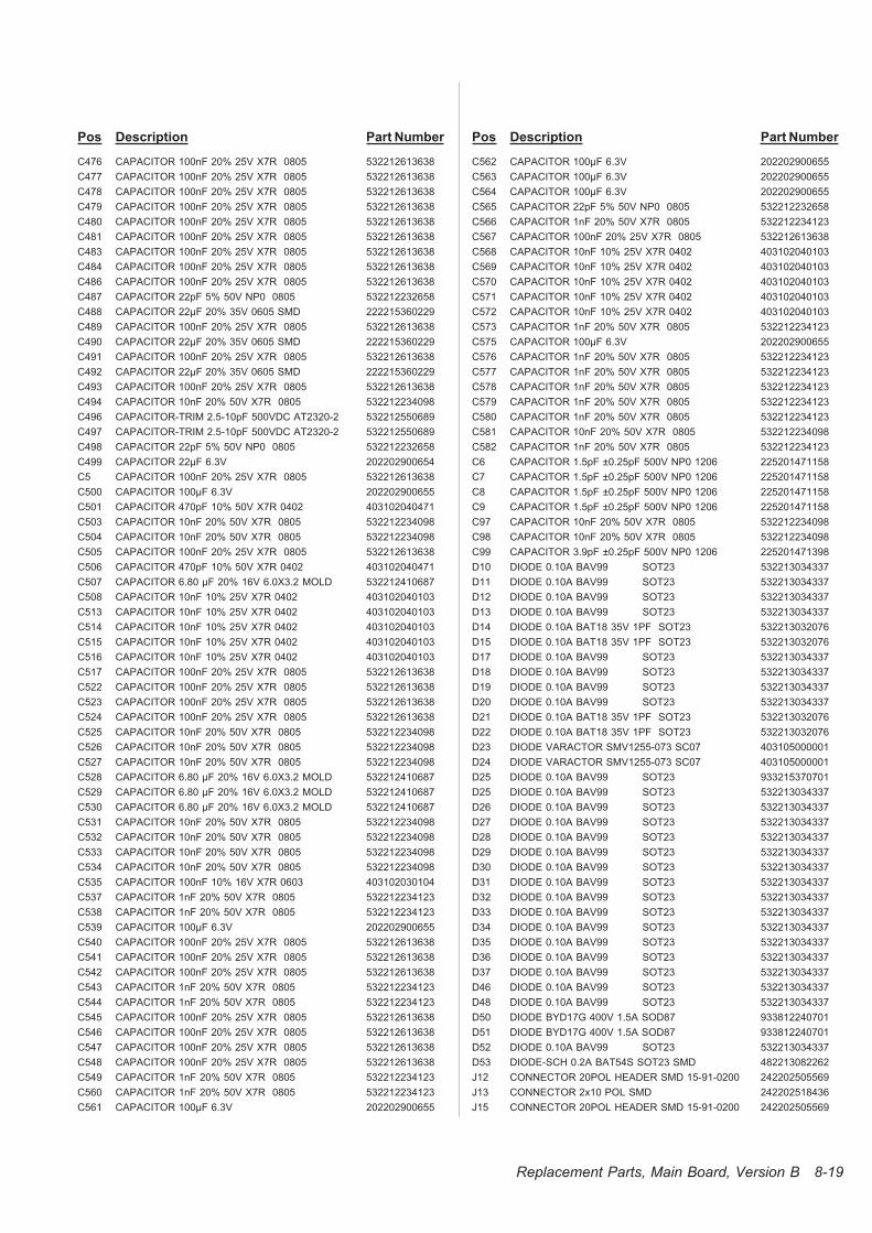
Pos Description Part Number
C476 CAPACITOR 100nF 20% 25V X7R 0805 532212613638
C477 CAPACITOR 100nF 20% 25V X7R 0805 532212613638
C478 CAPACITOR 100nF 20% 25V X7R 0805 532212613638
C479 CAPACITOR 100nF 20% 25V X7R 0805 532212613638
C480 CAPACITOR 100nF 20% 25V X7R 0805 532212613638
C481 CAPACITOR 100nF 20% 25V X7R 0805 532212613638
C483 CAPACITOR 100nF 20% 25V X7R 0805 532212613638
C484 CAPACITOR 100nF 20% 25V X7R 0805 532212613638
C486 CAPACITOR 100nF 20% 25V X7R 0805 532212613638
C487 CAPACITOR 22pF 5% 50V NP0 0805 532212232658
C488 CAPACITOR 22µF 20% 35V 0605 SMD 222215360229
C489 CAPACITOR 100nF 20% 25V X7R 0805 532212613638
C490 CAPACITOR 22µF 20% 35V 0605 SMD 222215360229
C491 CAPACITOR 100nF 20% 25V X7R 0805 532212613638
C492 CAPACITOR 22µF 20% 35V 0605 SMD 222215360229
C493 CAPACITOR 100nF 20% 25V X7R 0805 532212613638
C494 CAPACITOR 10nF 20% 50V X7R 0805 532212234098
C496 CAPACITOR-TRIM 2.5-10pF 500VDC AT2320-2 532212550689
C497 CAPACITOR-TRIM 2.5-10pF 500VDC AT2320-2 532212550689
C498 CAPACITOR 22pF 5% 50V NP0 0805 532212232658
C499 CAPACITOR 22µF 6.3V 202202900654
C5 CAPACITOR 100nF 20% 25V X7R 0805 532212613638
C500 CAPACITOR 100µF 6.3V 202202900655
C501 CAPACITOR 470pF 10% 50V X7R 0402 403102040471
C503 CAPACITOR 10nF 20% 50V X7R 0805 532212234098
C504 CAPACITOR 10nF 20% 50V X7R 0805 532212234098
C505 CAPACITOR 100nF 20% 25V X7R 0805 532212613638
C506 CAPACITOR 470pF 10% 50V X7R 0402 403102040471
C507 CAPACITOR 6.80 µF 20% 16V 6.0X3.2 MOLD 532212410687
C508 CAPACITOR 10nF 10% 25V X7R 0402 403102040103
C513 CAPACITOR 10nF 10% 25V X7R 0402 403102040103
C514 CAPACITOR 10nF 10% 25V X7R 0402 403102040103
C515 CAPACITOR 10nF 10% 25V X7R 0402 403102040103
C516 CAPACITOR 10nF 10% 25V X7R 0402 403102040103
C517 CAPACITOR 100nF 20% 25V X7R 0805 532212613638
C522 CAPACITOR 100nF 20% 25V X7R 0805 532212613638
C523 CAPACITOR 100nF 20% 25V X7R 0805 532212613638
C524 CAPACITOR 100nF 20% 25V X7R 0805 532212613638
C525 CAPACITOR 10nF 20% 50V X7R 0805 532212234098
C526 CAPACITOR 10nF 20% 50V X7R 0805 532212234098
C527 CAPACITOR 10nF 20% 50V X7R 0805 532212234098
C528 CAPACITOR 6.80 µF 20% 16V 6.0X3.2 MOLD 532212410687
C529 CAPACITOR 6.80 µF 20% 16V 6.0X3.2 MOLD 532212410687
C530 CAPACITOR 6.80 µF 20% 16V 6.0X3.2 MOLD 532212410687
C531 CAPACITOR 10nF 20% 50V X7R 0805 532212234098
C532 CAPACITOR 10nF 20% 50V X7R 0805 532212234098
C533 CAPACITOR 10nF 20% 50V X7R 0805 532212234098
C534 CAPACITOR 10nF 20% 50V X7R 0805 532212234098
C535 CAPACITOR 100nF 10% 16V X7R 0603 403102030104
C537 CAPACITOR 1nF 20% 50V X7R 0805 532212234123
C538 CAPACITOR 1nF 20% 50V X7R 0805 532212234123
C539 CAPACITOR 100µF 6.3V 202202900655
C540 CAPACITOR 100nF 20% 25V X7R 0805 532212613638
C541 CAPACITOR 100nF 20% 25V X7R 0805 532212613638
C542 CAPACITOR 100nF 20% 25V X7R 0805 532212613638
C543 CAPACITOR 1nF 20% 50V X7R 0805 532212234123
C544 CAPACITOR 1nF 20% 50V X7R 0805 532212234123
C545 CAPACITOR 100nF 20% 25V X7R 0805 532212613638
C546 CAPACITOR 100nF 20% 25V X7R 0805 532212613638
C547 CAPACITOR 100nF 20% 25V X7R 0805 532212613638
C548 CAPACITOR 100nF 20% 25V X7R 0805 532212613638
C549 CAPACITOR 1nF 20% 50V X7R 0805 532212234123
C560 CAPACITOR 1nF 20% 50V X7R 0805 532212234123
C561 CAPACITOR 100µF 6.3V 202202900655
Pos Description Part Number
C562 CAPACITOR 100µF 6.3V 202202900655
C563 CAPACITOR 100µF 6.3V 202202900655
C564 CAPACITOR 100µF 6.3V 202202900655
C565 CAPACITOR 22pF 5% 50V NP0 0805 532212232658
C566 CAPACITOR 1nF 20% 50V X7R 0805 532212234123
C567 CAPACITOR 100nF 20% 25V X7R 0805 532212613638
C568 CAPACITOR 10nF 10% 25V X7R 0402 403102040103
C569 CAPACITOR 10nF 10% 25V X7R 0402 403102040103
C570 CAPACITOR 10nF 10% 25V X7R 0402 403102040103
C571 CAPACITOR 10nF 10% 25V X7R 0402 403102040103
C572 CAPACITOR 10nF 10% 25V X7R 0402 403102040103
C573 CAPACITOR 1nF 20% 50V X7R 0805 532212234123
C575 CAPACITOR 100µF 6.3V 202202900655
C576 CAPACITOR 1nF 20% 50V X7R 0805 532212234123
C577 CAPACITOR 1nF 20% 50V X7R 0805 532212234123
C578 CAPACITOR 1nF 20% 50V X7R 0805 532212234123
C579 CAPACITOR 1nF 20% 50V X7R 0805 532212234123
C580 CAPACITOR 1nF 20% 50V X7R 0805 532212234123
C581 CAPACITOR 10nF 20% 50V X7R 0805 532212234098
C582 CAPACITOR 1nF 20% 50V X7R 0805 532212234123
C6 CAPACITOR 1.5pF ±0.25pF 500V NP0 1206 225201471158
C7 CAPACITOR 1.5pF ±0.25pF 500V NP0 1206 225201471158
C8 CAPACITOR 1.5pF ±0.25pF 500V NP0 1206 225201471158
C9 CAPACITOR 1.5pF ±0.25pF 500V NP0 1206 225201471158
C97 CAPACITOR 10nF 20% 50V X7R 0805 532212234098
C98 CAPACITOR 10nF 20% 50V X7R 0805 532212234098
C99 CAPACITOR 3.9pF ±0.25pF 500V NP0 1206 225201471398
D10 DIODE 0.10A BAV99 SOT23 532213034337
D11 DIODE 0.10A BAV99 SOT23 532213034337
D12 DIODE 0.10A BAV99 SOT23 532213034337
D13 DIODE 0.10A BAV99 SOT23 532213034337
D14 DIODE 0.10A BAT18 35V 1PF SOT23 532213032076
D15 DIODE 0.10A BAT18 35V 1PF SOT23 532213032076
D17 DIODE 0.10A BAV99 SOT23 532213034337
D18 DIODE 0.10A BAV99 SOT23 532213034337
D19 DIODE 0.10A BAV99 SOT23 532213034337
D20 DIODE 0.10A BAV99 SOT23 532213034337
D21 DIODE 0.10A BAT18 35V 1PF SOT23 532213032076
D22 DIODE 0.10A BAT18 35V 1PF SOT23 532213032076
D23 DIODE VARACTOR SMV1255-073 SC07 403105000001
D24 DIODE VARACTOR SMV1255-073 SC07 403105000001
D25 DIODE 0.10A BAV99 SOT23 933215370701
D25 DIODE 0.10A BAV99 SOT23 532213034337
D26 DIODE 0.10A BAV99 SOT23 532213034337
D27 DIODE 0.10A BAV99 SOT23 532213034337
D28 DIODE 0.10A BAV99 SOT23 532213034337
D29 DIODE 0.10A BAV99 SOT23 532213034337
D30 DIODE 0.10A BAV99 SOT23 532213034337
D31 DIODE 0.10A BAV99 SOT23 532213034337
D32 DIODE 0.10A BAV99 SOT23 532213034337
D33 DIODE 0.10A BAV99 SOT23 532213034337
D34 DIODE 0.10A BAV99 SOT23 532213034337
D35 DIODE 0.10A BAV99 SOT23 532213034337
D36 DIODE 0.10A BAV99 SOT23 532213034337
D37 DIODE 0.10A BAV99 SOT23 532213034337
D46 DIODE 0.10A BAV99 SOT23 532213034337
D48 DIODE 0.10A BAV99 SOT23 532213034337
D50 DIODE BYD17G 400V 1.5A SOD87 933812240701
D51 DIODE BYD17G 400V 1.5A SOD87 933812240701
D52 DIODE 0.10A BAV99 SOT23 532213034337
D53 DIODE-SCH 0.2A BAT54S SOT23 SMD 482213082262
J12 CONNECTOR 20POL HEADER SMD 15-91-0200 242202505569
J13 CONNECTOR 2x10 POL SMD 242202518436
J15 CONNECTOR 20POL HEADER SMD 15-91-0200 242202505569
Replacement Parts, Main Board, Version B 8-19
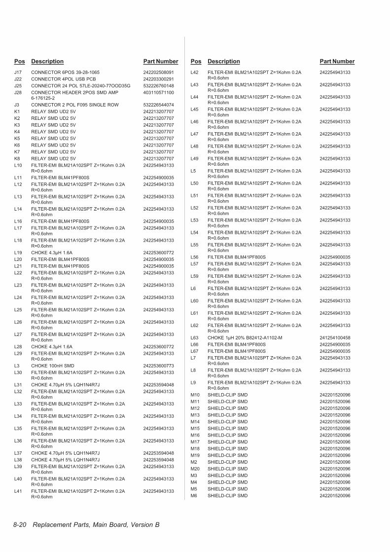
Pos Description Part Number
J17 CONNECTOR 6POS 39-28-1065 242202508091
J22 CONNECTOR 4POL USB PCB 242203300291
J25 CONNECTOR 24 POL 57LE-20240-77OOD35G 532226760148
J28 CONNECTOR HEADER 2POS SMD AMP
6-176125-2
403110571100
J3 CONNECTOR 2 POL F095 SINGLE ROW 532226544074
K1 RELAY SMD UD2 5V 242213207707
K2 RELAY SMD UD2 5V 242213207707
K3 RELAY SMD UD2 5V 242213207707
K4 RELAY SMD UD2 5V 242213207707
K5 RELAY SMD UD2 5V 242213207707
K6 RELAY SMD UD2 5V 242213207707
K7 RELAY SMD UD2 5V 242213207707
K8 RELAY SMD UD2 5V 242213207707
L10 FILTER-EMI BLM21A102SPT Z=1Kohm 0.2A
R=0.6ohm
242254943133
L11 FILTER-EMI BLM41PF800S 242254900035
L12 FILTER-EMI BLM21A102SPT Z=1Kohm 0.2A
R=0.6ohm
242254943133
L13 FILTER-EMI BLM21A102SPT Z=1Kohm 0.2A
R=0.6ohm
242254943133
L14 FILTER-EMI BLM21A102SPT Z=1Kohm 0.2A
R=0.6ohm
242254943133
L16 FILTER-EMI BLM41PF800S 242254900035
L17 FILTER-EMI BLM21A102SPT Z=1Kohm 0.2A
R=0.6ohm
242254943133
L18 FILTER-EMI BLM21A102SPT Z=1Kohm 0.2A
R=0.6ohm
242254943133
L19 CHOKE 4.3µH 1.6A 242253600772
L20 FILTER-EMI BLM41PF800S 242254900035
L21 FILTER-EMI BLM41PF800S 242254900035
L22 FILTER-EMI BLM21A102SPT Z=1Kohm 0.2A
R=0.6ohm
242254943133
L23 FILTER-EMI BLM21A102SPT Z=1Kohm 0.2A
R=0.6ohm
242254943133
L24 FILTER-EMI BLM21A102SPT Z=1Kohm 0.2A
R=0.6ohm
242254943133
L25 FILTER-EMI BLM21A102SPT Z=1Kohm 0.2A
R=0.6ohm
242254943133
L26 FILTER-EMI BLM21A102SPT Z=1Kohm 0.2A
R=0.6ohm
242254943133
L27 FILTER-EMI BLM21A102SPT Z=1Kohm 0.2A
R=0.6ohm
242254943133
L28 CHOKE 4.3µH 1.6A 242253600772
L29 FILTER-EMI BLM21A102SPT Z=1Kohm 0.2A
R=0.6ohm
242254943133
L3 CHOKE 100nH SMD 242253600773
L30 FILTER-EMI BLM21A102SPT Z=1Kohm 0.2A
R=0.6ohm
242254943133
L31 CHOKE 4.70µH 5% LQH1N4R7J 242253594048
L32 FILTER-EMI BLM21A102SPT Z=1Kohm 0.2A
R=0.6ohm
242254943133
L33 FILTER-EMI BLM21A102SPT Z=1Kohm 0.2A
R=0.6ohm
242254943133
L34 FILTER-EMI BLM21A102SPT Z=1Kohm 0.2A
R=0.6ohm
242254943133
L35 FILTER-EMI BLM21A102SPT Z=1Kohm 0.2A
R=0.6ohm
242254943133
L36 FILTER-EMI BLM21A102SPT Z=1Kohm 0.2A
R=0.6ohm
242254943133
L37 CHOKE 4.70µH 5% LQH1N4R7J 242253594048
L38 CHOKE 4.70µH 5% LQH1N4R7J 242253594048
L39 FILTER-EMI BLM21A102SPT Z=1Kohm 0.2A
R=0.6ohm
242254943133
L40 FILTER-EMI BLM21A102SPT Z=1Kohm 0.2A
R=0.6ohm
242254943133
L41 FILTER-EMI BLM21A102SPT Z=1Kohm 0.2A
R=0.6ohm
242254943133
Pos Description Part Number
L42 FILTER-EMI BLM21A102SPT Z=1Kohm 0.2A
R=0.6ohm
242254943133
L43 FILTER-EMI BLM21A102SPT Z=1Kohm 0.2A
R=0.6ohm
242254943133
L44 FILTER-EMI BLM21A102SPT Z=1Kohm 0.2A
R=0.6ohm
242254943133
L45 FILTER-EMI BLM21A102SPT Z=1Kohm 0.2A
R=0.6ohm
242254943133
L46 FILTER-EMI BLM21A102SPT Z=1Kohm 0.2A
R=0.6ohm
242254943133
L47 FILTER-EMI BLM21A102SPT Z=1Kohm 0.2A
R=0.6ohm
242254943133
L48 FILTER-EMI BLM21A102SPT Z=1Kohm 0.2A
R=0.6ohm
242254943133
L49 FILTER-EMI BLM21A102SPT Z=1Kohm 0.2A
R=0.6ohm
242254943133
L5 FILTER-EMI BLM21A102SPT Z=1Kohm 0.2A
R=0.6ohm
242254943133
L50 FILTER-EMI BLM21A102SPT Z=1Kohm 0.2A
R=0.6ohm
242254943133
L51 FILTER-EMI BLM21A102SPT Z=1Kohm 0.2A
R=0.6ohm
242254943133
L52 FILTER-EMI BLM21A102SPT Z=1Kohm 0.2A
R=0.6ohm
242254943133
L53 FILTER-EMI BLM21A102SPT Z=1Kohm 0.2A
R=0.6ohm
242254943133
L54 FILTER-EMI BLM21A102SPT Z=1Kohm 0.2A
R=0.6ohm
242254943133
L55 FILTER-EMI BLM21A102SPT Z=1Kohm 0.2A
R=0.6ohm
242254943133
L56 FILTER-EMI BLM41PF800S 242254900035
L57 FILTER-EMI BLM21A102SPT Z=1Kohm 0.2A
R=0.6ohm
242254943133
L59 FILTER-EMI BLM21A102SPT Z=1Kohm 0.2A
R=0.6ohm
242254943133
L6 FILTER-EMI BLM21A102SPT Z=1Kohm 0.2A
R=0.6ohm
242254943133
L60 FILTER-EMI BLM21A102SPT Z=1Kohm 0.2A
R=0.6ohm
242254943133
L61 FILTER-EMI BLM21A102SPT Z=1Kohm 0.2A
R=0.6ohm
242254943133
L62 FILTER-EMI BLM21A102SPT Z=1Kohm 0.2A
R=0.6ohm
242254943133
L63 CHOKE 1µH 20% B82412-A1102-M 241254100458
L66 FILTER-EMI BLM41PF800S 242254900035
L67 FILTER-EMI BLM41PF800S 242254900035
L7 FILTER-EMI BLM21A102SPT Z=1Kohm 0.2A
R=0.6ohm
242254943133
L8 FILTER-EMI BLM21A102SPT Z=1Kohm 0.2A
R=0.6ohm
242254943133
L9 FILTER-EMI BLM21A102SPT Z=1Kohm 0.2A
R=0.6ohm
242254943133
M10 SHIELD-CLIP SMD 242201520096
M11 SHIELD-CLIP SMD 242201520096
M12 SHIELD-CLIP SMD 242201520096
M13 SHIELD-CLIP SMD 242201520096
M14 SHIELD-CLIP SMD 242201520096
M15 SHIELD-CLIP SMD 242201520096
M16 SHIELD-CLIP SMD 242201520096
M17 SHIELD-CLIP SMD 242201520096
M18 SHIELD-CLIP SMD 242201520096
M19 SHIELD-CLIP SMD 242201520096
M2 SHIELD-CLIP SMD 242201520096
M20 SHIELD-CLIP SMD 242201520096
M3 SHIELD-CLIP SMD 242201520096
M4 SHIELD-CLIP SMD 242201520096
M5 SHIELD-CLIP SMD 242201520096
M6 SHIELD-CLIP SMD 242201520096
8-20 Replacement Parts, Main Board, Version B
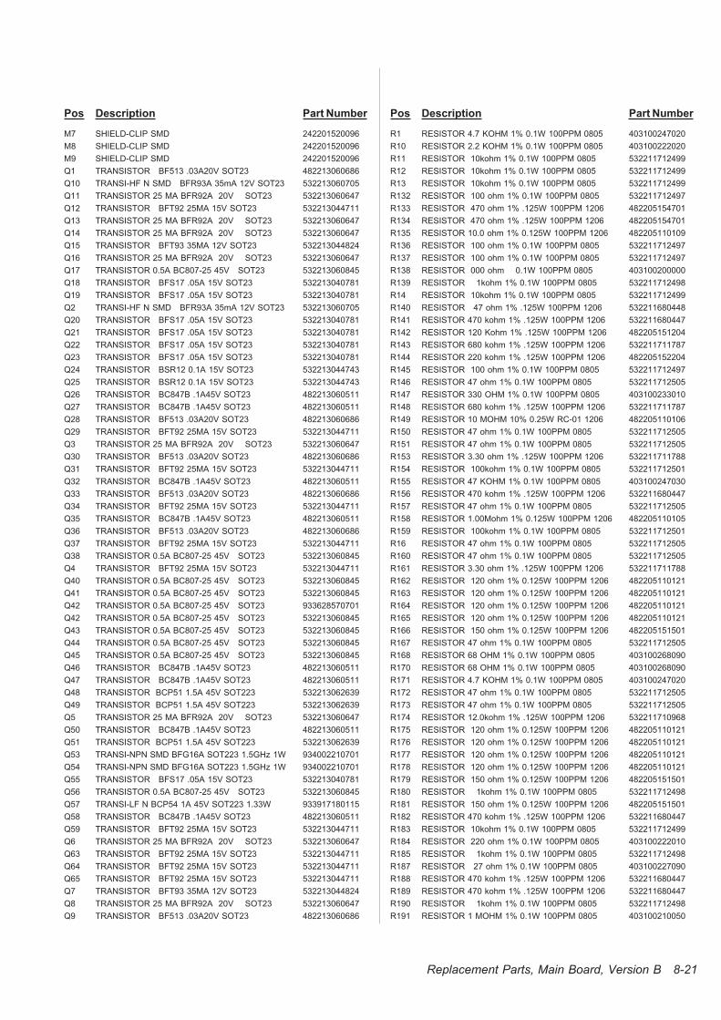
Pos Description Part Number
M7 SHIELD-CLIP SMD 242201520096
M8 SHIELD-CLIP SMD 242201520096
M9 SHIELD-CLIP SMD 242201520096
Q1 TRANSISTOR BF513 .03A20V SOT23 482213060686
Q10 TRANSI-HF N SMD BFR93A 35mA 12V SOT23 532213060705
Q11 TRANSISTOR 25 MA BFR92A 20V SOT23 532213060647
Q12 TRANSISTOR BFT92 25MA 15V SOT23 532213044711
Q13 TRANSISTOR 25 MA BFR92A 20V SOT23 532213060647
Q14 TRANSISTOR 25 MA BFR92A 20V SOT23 532213060647
Q15 TRANSISTOR BFT93 35MA 12V SOT23 532213044824
Q16 TRANSISTOR 25 MA BFR92A 20V SOT23 532213060647
Q17 TRANSISTOR 0.5A BC807-25 45V SOT23 532213060845
Q18 TRANSISTOR BFS17 .05A 15V SOT23 532213040781
Q19 TRANSISTOR BFS17 .05A 15V SOT23 532213040781
Q2 TRANSI-HF N SMD BFR93A 35mA 12V SOT23 532213060705
Q20 TRANSISTOR BFS17 .05A 15V SOT23 532213040781
Q21 TRANSISTOR BFS17 .05A 15V SOT23 532213040781
Q22 TRANSISTOR BFS17 .05A 15V SOT23 532213040781
Q23 TRANSISTOR BFS17 .05A 15V SOT23 532213040781
Q24 TRANSISTOR BSR12 0.1A 15V SOT23 532213044743
Q25 TRANSISTOR BSR12 0.1A 15V SOT23 532213044743
Q26 TRANSISTOR BC847B .1A45V SOT23 482213060511
Q27 TRANSISTOR BC847B .1A45V SOT23 482213060511
Q28 TRANSISTOR BF513 .03A20V SOT23 482213060686
Q29 TRANSISTOR BFT92 25MA 15V SOT23 532213044711
Q3 TRANSISTOR 25 MA BFR92A 20V SOT23 532213060647
Q30 TRANSISTOR BF513 .03A20V SOT23 482213060686
Q31 TRANSISTOR BFT92 25MA 15V SOT23 532213044711
Q32 TRANSISTOR BC847B .1A45V SOT23 482213060511
Q33 TRANSISTOR BF513 .03A20V SOT23 482213060686
Q34 TRANSISTOR BFT92 25MA 15V SOT23 532213044711
Q35 TRANSISTOR BC847B .1A45V SOT23 482213060511
Q36 TRANSISTOR BF513 .03A20V SOT23 482213060686
Q37 TRANSISTOR BFT92 25MA 15V SOT23 532213044711
Q38 TRANSISTOR 0.5A BC807-25 45V SOT23 532213060845
Q4 TRANSISTOR BFT92 25MA 15V SOT23 532213044711
Q40 TRANSISTOR 0.5A BC807-25 45V SOT23 532213060845
Q41 TRANSISTOR 0.5A BC807-25 45V SOT23 532213060845
Q42 TRANSISTOR 0.5A BC807-25 45V SOT23 933628570701
Q42 TRANSISTOR 0.5A BC807-25 45V SOT23 532213060845
Q43 TRANSISTOR 0.5A BC807-25 45V SOT23 532213060845
Q44 TRANSISTOR 0.5A BC807-25 45V SOT23 532213060845
Q45 TRANSISTOR 0.5A BC807-25 45V SOT23 532213060845
Q46 TRANSISTOR BC847B .1A45V SOT23 482213060511
Q47 TRANSISTOR BC847B .1A45V SOT23 482213060511
Q48 TRANSISTOR BCP51 1.5A 45V SOT223 532213062639
Q49 TRANSISTOR BCP51 1.5A 45V SOT223 532213062639
Q5 TRANSISTOR 25 MA BFR92A 20V SOT23 532213060647
Q50 TRANSISTOR BC847B .1A45V SOT23 482213060511
Q51 TRANSISTOR BCP51 1.5A 45V SOT223 532213062639
Q53 TRANSI-NPN SMD BFG16A SOT223 1.5GHz 1W 934002210701
Q54 TRANSI-NPN SMD BFG16A SOT223 1.5GHz 1W 934002210701
Q55 TRANSISTOR BFS17 .05A 15V SOT23 532213040781
Q56 TRANSISTOR 0.5A BC807-25 45V SOT23 532213060845
Q57 TRANSI-LF N BCP54 1A 45V SOT223 1.33W 933917180115
Q58 TRANSISTOR BC847B .1A45V SOT23 482213060511
Q59 TRANSISTOR BFT92 25MA 15V SOT23 532213044711
Q6 TRANSISTOR 25 MA BFR92A 20V SOT23 532213060647
Q63 TRANSISTOR BFT92 25MA 15V SOT23 532213044711
Q64 TRANSISTOR BFT92 25MA 15V SOT23 532213044711
Q65 TRANSISTOR BFT92 25MA 15V SOT23 532213044711
Q7 TRANSISTOR BFT93 35MA 12V SOT23 532213044824
Q8 TRANSISTOR 25 MA BFR92A 20V SOT23 532213060647
Q9 TRANSISTOR BF513 .03A20V SOT23 482213060686
Pos Description Part Number
R1 RESISTOR 4.7 KOHM 1% 0.1W 100PPM 0805 403100247020
R10 RESISTOR 2.2 KOHM 1% 0.1W 100PPM 0805 403100222020
R11 RESISTOR 10kohm 1% 0.1W 100PPM 0805 532211712499
R12 RESISTOR 10kohm 1% 0.1W 100PPM 0805 532211712499
R13 RESISTOR 10kohm 1% 0.1W 100PPM 0805 532211712499
R132 RESISTOR 100 ohm 1% 0.1W 100PPM 0805 532211712497
R133 RESISTOR 470 ohm 1% .125W 100PPM 1206 482205154701
R134 RESISTOR 470 ohm 1% .125W 100PPM 1206 482205154701
R135 RESISTOR 10.0 ohm 1% 0.125W 100PPM 1206 482205110109
R136 RESISTOR 100 ohm 1% 0.1W 100PPM 0805 532211712497
R137 RESISTOR 100 ohm 1% 0.1W 100PPM 0805 532211712497
R138 RESISTOR 000 ohm 0.1W 100PPM 0805 403100200000
R139 RESISTOR 1kohm 1% 0.1W 100PPM 0805 532211712498
R14 RESISTOR 10kohm 1% 0.1W 100PPM 0805 532211712499
R140 RESISTOR 47 ohm 1% .125W 100PPM 1206 532211680448
R141 RESISTOR 470 kohm 1% .125W 100PPM 1206 532211680447
R142 RESISTOR 120 Kohm 1% .125W 100PPM 1206 482205151204
R143 RESISTOR 680 kohm 1% .125W 100PPM 1206 532211711787
R144 RESISTOR 220 kohm 1% .125W 100PPM 1206 482205152204
R145 RESISTOR 100 ohm 1% 0.1W 100PPM 0805 532211712497
R146 RESISTOR 47 ohm 1% 0.1W 100PPM 0805 532211712505
R147 RESISTOR 330 OHM 1% 0.1W 100PPM 0805 403100233010
R148 RESISTOR 680 kohm 1% .125W 100PPM 1206 532211711787
R149 RESISTOR 10 MOHM 10% 0.25W RC-01 1206 482205110106
R150 RESISTOR 47 ohm 1% 0.1W 100PPM 0805 532211712505
R151 RESISTOR 47 ohm 1% 0.1W 100PPM 0805 532211712505
R153 RESISTOR 3.30 ohm 1% .125W 100PPM 1206 532211711788
R154 RESISTOR 100kohm 1% 0.1W 100PPM 0805 532211712501
R155 RESISTOR 47 KOHM 1% 0.1W 100PPM 0805 403100247030
R156 RESISTOR 470 kohm 1% .125W 100PPM 1206 532211680447
R157 RESISTOR 47 ohm 1% 0.1W 100PPM 0805 532211712505
R158 RESISTOR 1.00Mohm 1% 0.125W 100PPM 1206 482205110105
R159 RESISTOR 100kohm 1% 0.1W 100PPM 0805 532211712501
R16 RESISTOR 47 ohm 1% 0.1W 100PPM 0805 532211712505
R160 RESISTOR 47 ohm 1% 0.1W 100PPM 0805 532211712505
R161 RESISTOR 3.30 ohm 1% .125W 100PPM 1206 532211711788
R162 RESISTOR 120 ohm 1% 0.125W 100PPM 1206 482205110121
R163 RESISTOR 120 ohm 1% 0.125W 100PPM 1206 482205110121
R164 RESISTOR 120 ohm 1% 0.125W 100PPM 1206 482205110121
R165 RESISTOR 120 ohm 1% 0.125W 100PPM 1206 482205110121
R166 RESISTOR 150 ohm 1% 0.125W 100PPM 1206 482205151501
R167 RESISTOR 47 ohm 1% 0.1W 100PPM 0805 532211712505
R168 RESISTOR 68 OHM 1% 0.1W 100PPM 0805 403100268090
R170 RESISTOR 68 OHM 1% 0.1W 100PPM 0805 403100268090
R171 RESISTOR 4.7 KOHM 1% 0.1W 100PPM 0805 403100247020
R172 RESISTOR 47 ohm 1% 0.1W 100PPM 0805 532211712505
R173 RESISTOR 47 ohm 1% 0.1W 100PPM 0805 532211712505
R174 RESISTOR 12.0kohm 1% .125W 100PPM 1206 532211710968
R175 RESISTOR 120 ohm 1% 0.125W 100PPM 1206 482205110121
R176 RESISTOR 120 ohm 1% 0.125W 100PPM 1206 482205110121
R177 RESISTOR 120 ohm 1% 0.125W 100PPM 1206 482205110121
R178 RESISTOR 120 ohm 1% 0.125W 100PPM 1206 482205110121
R179 RESISTOR 150 ohm 1% 0.125W 100PPM 1206 482205151501
R180 RESISTOR 1kohm 1% 0.1W 100PPM 0805 532211712498
R181 RESISTOR 150 ohm 1% 0.125W 100PPM 1206 482205151501
R182 RESISTOR 470 kohm 1% .125W 100PPM 1206 532211680447
R183 RESISTOR 10kohm 1% 0.1W 100PPM 0805 532211712499
R184 RESISTOR 220 ohm 1% 0.1W 100PPM 0805 403100222010
R185 RESISTOR 1kohm 1% 0.1W 100PPM 0805 532211712498
R187 RESISTOR 27 ohm 1% 0.1W 100PPM 0805 403100227090
R188 RESISTOR 470 kohm 1% .125W 100PPM 1206 532211680447
R189 RESISTOR 470 kohm 1% .125W 100PPM 1206 532211680447
R190 RESISTOR 1kohm 1% 0.1W 100PPM 0805 532211712498
R191 RESISTOR 1 MOHM 1% 0.1W 100PPM 0805 403100210050
Replacement Parts, Main Board, Version B 8-21
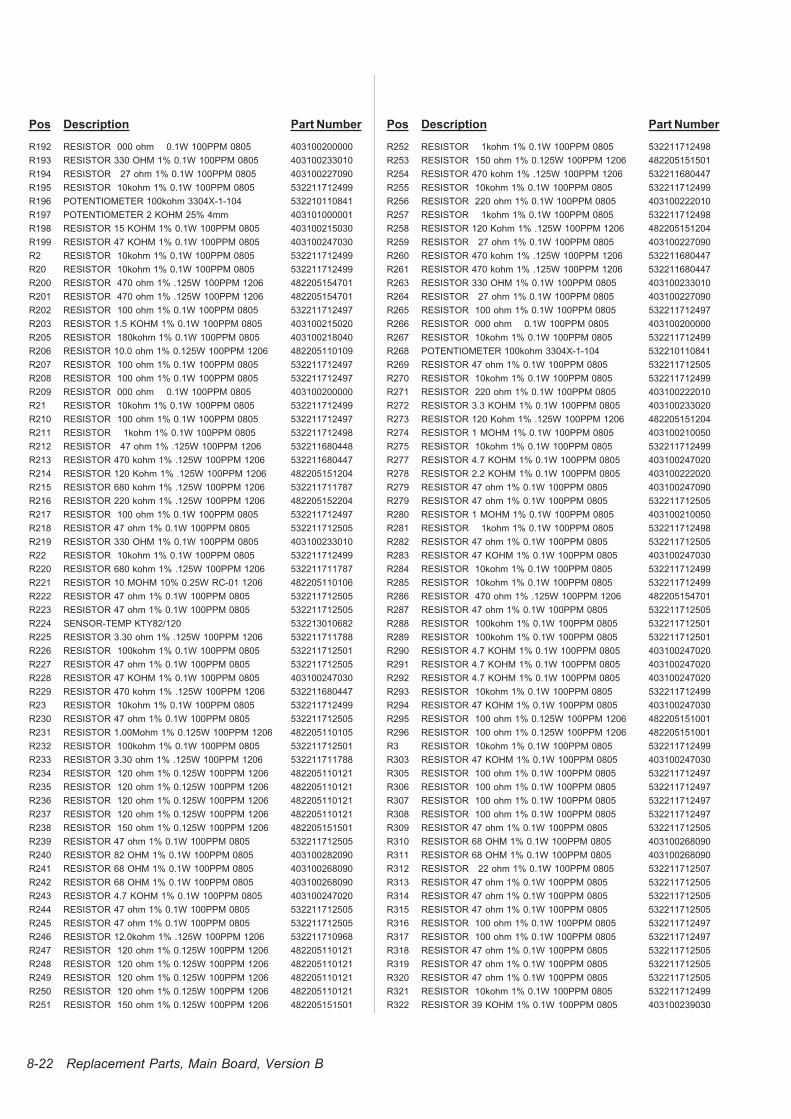
Pos Description Part Number
R192 RESISTOR 000 ohm 0.1W 100PPM 0805 403100200000
R193 RESISTOR 330 OHM 1% 0.1W 100PPM 0805 403100233010
R194 RESISTOR 27 ohm 1% 0.1W 100PPM 0805 403100227090
R195 RESISTOR 10kohm 1% 0.1W 100PPM 0805 532211712499
R196 POTENTIOMETER 100kohm 3304X-1-104 532210110841
R197 POTENTIOMETER 2 KOHM 25% 4mm 403101000001
R198 RESISTOR 15 KOHM 1% 0.1W 100PPM 0805 403100215030
R199 RESISTOR 47 KOHM 1% 0.1W 100PPM 0805 403100247030
R2 RESISTOR 10kohm 1% 0.1W 100PPM 0805 532211712499
R20 RESISTOR 10kohm 1% 0.1W 100PPM 0805 532211712499
R200 RESISTOR 470 ohm 1% .125W 100PPM 1206 482205154701
R201 RESISTOR 470 ohm 1% .125W 100PPM 1206 482205154701
R202 RESISTOR 100 ohm 1% 0.1W 100PPM 0805 532211712497
R203 RESISTOR 1.5 KOHM 1% 0.1W 100PPM 0805 403100215020
R205 RESISTOR 180kohm 1% 0.1W 100PPM 0805 403100218040
R206 RESISTOR 10.0 ohm 1% 0.125W 100PPM 1206 482205110109
R207 RESISTOR 100 ohm 1% 0.1W 100PPM 0805 532211712497
R208 RESISTOR 100 ohm 1% 0.1W 100PPM 0805 532211712497
R209 RESISTOR 000 ohm 0.1W 100PPM 0805 403100200000
R21 RESISTOR 10kohm 1% 0.1W 100PPM 0805 532211712499
R210 RESISTOR 100 ohm 1% 0.1W 100PPM 0805 532211712497
R211 RESISTOR 1kohm 1% 0.1W 100PPM 0805 532211712498
R212 RESISTOR 47 ohm 1% .125W 100PPM 1206 532211680448
R213 RESISTOR 470 kohm 1% .125W 100PPM 1206 532211680447
R214 RESISTOR 120 Kohm 1% .125W 100PPM 1206 482205151204
R215 RESISTOR 680 kohm 1% .125W 100PPM 1206 532211711787
R216 RESISTOR 220 kohm 1% .125W 100PPM 1206 482205152204
R217 RESISTOR 100 ohm 1% 0.1W 100PPM 0805 532211712497
R218 RESISTOR 47 ohm 1% 0.1W 100PPM 0805 532211712505
R219 RESISTOR 330 OHM 1% 0.1W 100PPM 0805 403100233010
R22 RESISTOR 10kohm 1% 0.1W 100PPM 0805 532211712499
R220 RESISTOR 680 kohm 1% .125W 100PPM 1206 532211711787
R221 RESISTOR 10 MOHM 10% 0.25W RC-01 1206 482205110106
R222 RESISTOR 47 ohm 1% 0.1W 100PPM 0805 532211712505
R223 RESISTOR 47 ohm 1% 0.1W 100PPM 0805 532211712505
R224 SENSOR-TEMP KTY82/120 532213010682
R225 RESISTOR 3.30 ohm 1% .125W 100PPM 1206 532211711788
R226 RESISTOR 100kohm 1% 0.1W 100PPM 0805 532211712501
R227 RESISTOR 47 ohm 1% 0.1W 100PPM 0805 532211712505
R228 RESISTOR 47 KOHM 1% 0.1W 100PPM 0805 403100247030
R229 RESISTOR 470 kohm 1% .125W 100PPM 1206 532211680447
R23 RESISTOR 10kohm 1% 0.1W 100PPM 0805 532211712499
R230 RESISTOR 47 ohm 1% 0.1W 100PPM 0805 532211712505
R231 RESISTOR 1.00Mohm 1% 0.125W 100PPM 1206 482205110105
R232 RESISTOR 100kohm 1% 0.1W 100PPM 0805 532211712501
R233 RESISTOR 3.30 ohm 1% .125W 100PPM 1206 532211711788
R234 RESISTOR 120 ohm 1% 0.125W 100PPM 1206 482205110121
R235 RESISTOR 120 ohm 1% 0.125W 100PPM 1206 482205110121
R236 RESISTOR 120 ohm 1% 0.125W 100PPM 1206 482205110121
R237 RESISTOR 120 ohm 1% 0.125W 100PPM 1206 482205110121
R238 RESISTOR 150 ohm 1% 0.125W 100PPM 1206 482205151501
R239 RESISTOR 47 ohm 1% 0.1W 100PPM 0805 532211712505
R240 RESISTOR 82 OHM 1% 0.1W 100PPM 0805 403100282090
R241 RESISTOR 68 OHM 1% 0.1W 100PPM 0805 403100268090
R242 RESISTOR 68 OHM 1% 0.1W 100PPM 0805 403100268090
R243 RESISTOR 4.7 KOHM 1% 0.1W 100PPM 0805 403100247020
R244 RESISTOR 47 ohm 1% 0.1W 100PPM 0805 532211712505
R245 RESISTOR 47 ohm 1% 0.1W 100PPM 0805 532211712505
R246 RESISTOR 12.0kohm 1% .125W 100PPM 1206 532211710968
R247 RESISTOR 120 ohm 1% 0.125W 100PPM 1206 482205110121
R248 RESISTOR 120 ohm 1% 0.125W 100PPM 1206 482205110121
R249 RESISTOR 120 ohm 1% 0.125W 100PPM 1206 482205110121
R250 RESISTOR 120 ohm 1% 0.125W 100PPM 1206 482205110121
R251 RESISTOR 150 ohm 1% 0.125W 100PPM 1206 482205151501
Pos Description Part Number
R252 RESISTOR 1kohm 1% 0.1W 100PPM 0805 532211712498
R253 RESISTOR 150 ohm 1% 0.125W 100PPM 1206 482205151501
R254 RESISTOR 470 kohm 1% .125W 100PPM 1206 532211680447
R255 RESISTOR 10kohm 1% 0.1W 100PPM 0805 532211712499
R256 RESISTOR 220 ohm 1% 0.1W 100PPM 0805 403100222010
R257 RESISTOR 1kohm 1% 0.1W 100PPM 0805 532211712498
R258 RESISTOR 120 Kohm 1% .125W 100PPM 1206 482205151204
R259 RESISTOR 27 ohm 1% 0.1W 100PPM 0805 403100227090
R260 RESISTOR 470 kohm 1% .125W 100PPM 1206 532211680447
R261 RESISTOR 470 kohm 1% .125W 100PPM 1206 532211680447
R263 RESISTOR 330 OHM 1% 0.1W 100PPM 0805 403100233010
R264 RESISTOR 27 ohm 1% 0.1W 100PPM 0805 403100227090
R265 RESISTOR 100 ohm 1% 0.1W 100PPM 0805 532211712497
R266 RESISTOR 000 ohm 0.1W 100PPM 0805 403100200000
R267 RESISTOR 10kohm 1% 0.1W 100PPM 0805 532211712499
R268 POTENTIOMETER 100kohm 3304X-1-104 532210110841
R269 RESISTOR 47 ohm 1% 0.1W 100PPM 0805 532211712505
R270 RESISTOR 10kohm 1% 0.1W 100PPM 0805 532211712499
R271 RESISTOR 220 ohm 1% 0.1W 100PPM 0805 403100222010
R272 RESISTOR 3.3 KOHM 1% 0.1W 100PPM 0805 403100233020
R273 RESISTOR 120 Kohm 1% .125W 100PPM 1206 482205151204
R274 RESISTOR 1 MOHM 1% 0.1W 100PPM 0805 403100210050
R275 RESISTOR 10kohm 1% 0.1W 100PPM 0805 532211712499
R277 RESISTOR 4.7 KOHM 1% 0.1W 100PPM 0805 403100247020
R278 RESISTOR 2.2 KOHM 1% 0.1W 100PPM 0805 403100222020
R279 RESISTOR 47 ohm 1% 0.1W 100PPM 0805 403100247090
R279 RESISTOR 47 ohm 1% 0.1W 100PPM 0805 532211712505
R280 RESISTOR 1 MOHM 1% 0.1W 100PPM 0805 403100210050
R281 RESISTOR 1kohm 1% 0.1W 100PPM 0805 532211712498
R282 RESISTOR 47 ohm 1% 0.1W 100PPM 0805 532211712505
R283 RESISTOR 47 KOHM 1% 0.1W 100PPM 0805 403100247030
R284 RESISTOR 10kohm 1% 0.1W 100PPM 0805 532211712499
R285 RESISTOR 10kohm 1% 0.1W 100PPM 0805 532211712499
R286 RESISTOR 470 ohm 1% .125W 100PPM 1206 482205154701
R287 RESISTOR 47 ohm 1% 0.1W 100PPM 0805 532211712505
R288 RESISTOR 100kohm 1% 0.1W 100PPM 0805 532211712501
R289 RESISTOR 100kohm 1% 0.1W 100PPM 0805 532211712501
R290 RESISTOR 4.7 KOHM 1% 0.1W 100PPM 0805 403100247020
R291 RESISTOR 4.7 KOHM 1% 0.1W 100PPM 0805 403100247020
R292 RESISTOR 4.7 KOHM 1% 0.1W 100PPM 0805 403100247020
R293 RESISTOR 10kohm 1% 0.1W 100PPM 0805 532211712499
R294 RESISTOR 47 KOHM 1% 0.1W 100PPM 0805 403100247030
R295 RESISTOR 100 ohm 1% 0.125W 100PPM 1206 482205151001
R296 RESISTOR 100 ohm 1% 0.125W 100PPM 1206 482205151001
R3 RESISTOR 10kohm 1% 0.1W 100PPM 0805 532211712499
R303 RESISTOR 47 KOHM 1% 0.1W 100PPM 0805 403100247030
R305 RESISTOR 100 ohm 1% 0.1W 100PPM 0805 532211712497
R306 RESISTOR 100 ohm 1% 0.1W 100PPM 0805 532211712497
R307 RESISTOR 100 ohm 1% 0.1W 100PPM 0805 532211712497
R308 RESISTOR 100 ohm 1% 0.1W 100PPM 0805 532211712497
R309 RESISTOR 47 ohm 1% 0.1W 100PPM 0805 532211712505
R310 RESISTOR 68 OHM 1% 0.1W 100PPM 0805 403100268090
R311 RESISTOR 68 OHM 1% 0.1W 100PPM 0805 403100268090
R312 RESISTOR 22 ohm 1% 0.1W 100PPM 0805 532211712507
R313 RESISTOR 47 ohm 1% 0.1W 100PPM 0805 532211712505
R314 RESISTOR 47 ohm 1% 0.1W 100PPM 0805 532211712505
R315 RESISTOR 47 ohm 1% 0.1W 100PPM 0805 532211712505
R316 RESISTOR 100 ohm 1% 0.1W 100PPM 0805 532211712497
R317 RESISTOR 100 ohm 1% 0.1W 100PPM 0805 532211712497
R318 RESISTOR 47 ohm 1% 0.1W 100PPM 0805 532211712505
R319 RESISTOR 47 ohm 1% 0.1W 100PPM 0805 532211712505
R320 RESISTOR 47 ohm 1% 0.1W 100PPM 0805 532211712505
R321 RESISTOR 10kohm 1% 0.1W 100PPM 0805 532211712499
R322 RESISTOR 39 KOHM 1% 0.1W 100PPM 0805 403100239030
8-22 Replacement Parts, Main Board, Version B
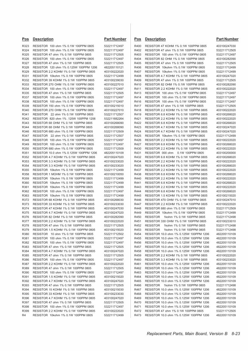
Pos Description Part Number
R323 RESISTOR 100 ohm 1% 0.1W 100PPM 0805 532211712497
R324 RESISTOR 100 ohm 1% 0.1W 100PPM 0805 532211712497
R325 RESISTOR 47 ohm 1% 0.1W 100PPM 0805 532211712505
R326 RESISTOR 100 ohm 1% 0.1W 100PPM 0805 532211712497
R327 RESISTOR 47 ohm 1% 0.1W 100PPM 0805 532211712505
R328 RESISTOR 120 ohm 1% 0.125W 100PPM 1206 482205110121
R329 RESISTOR 2.2 KOHM 1% 0.1W 100PPM 0805 403100222020
R331 RESISTOR 10kohm 1% 0.1W 100PPM 0805 532211712499
R332 RESISTOR 39 KOHM 1% 0.1W 100PPM 0805 403100239030
R333 RESISTOR 270 OHM 1% 0.1W 100PPM 0805 403100227010
R334 RESISTOR 100 ohm 1% 0.1W 100PPM 0805 532211712497
R335 RESISTOR 47 ohm 1% 0.1W 100PPM 0805 532211712505
R337 RESISTOR 100 ohm 1% 0.1W 100PPM 0805 532211712497
R338 RESISTOR 100 ohm 1% 0.1W 100PPM 0805 532211712497
R339 RESISTOR 150 ohm 1% 0.1W 100PPM 0805 403100215010
R340 RESISTOR 270 OHM 1% 0.1W 100PPM 0805 403100227010
R341 RESISTOR 22 ohm 1% 0.1W 100PPM 0805 532211712507
R342 RESISTOR 820 ohm 1% .125W 100PPM 1206 532211682264
R343 RESISTOR 68 OHM 1% 0.1W 100PPM 0805 403100268090
R344 RESISTOR 68 OHM 1% 0.1W 100PPM 0805 403100268090
R346 RESISTOR 680 ohm 1% 0.1W 100PPM 0805 532211712509
R347 RESISTOR 22 ohm 1% 0.1W 100PPM 0805 532211712507
R348 RESISTOR 100 ohm 1% 0.1W 100PPM 0805 532211712497
R349 RESISTOR 100 ohm 1% 0.1W 100PPM 0805 532211712497
R350 RESISTOR 680 ohm 1% 0.1W 100PPM 0805 532211712509
R351 RESISTOR 10.0 ohm 1% 0.125W 100PPM 1206 482205110109
R352 RESISTOR 4.7 KOHM 1% 0.1W 100PPM 0805 403100247020
R353 RESISTOR 3.3 KOHM 1% 0.1W 100PPM 0805 403100233020
R354 RESISTOR 3.3 KOHM 1% 0.1W 100PPM 0805 403100233020
R355 RESISTOR 10kohm 1% 0.1W 100PPM 0805 532211712499
R358 RESISTOR 1 MOHM 1% 0.1W 100PPM 0805 403100210050
R359 RESISTOR 10kohm 1% 0.1W 100PPM 0805 532211712499
R360 RESISTOR 10kohm 1% 0.1W 100PPM 0805 532211712499
R361 RESISTOR 10kohm 1% 0.1W 100PPM 0805 532211712499
R362 RESISTOR 100 ohm 1% 0.1W 100PPM 0805 532211712497
R363 RESISTOR 10kohm 1% 0.1W 100PPM 0805 532211712499
R372 RESISTOR 68 KOHM 1% 0.1W 100PPM 0805 403100268030
R373 RESISTOR 33 KOHM 1% 0.1W 100PPM 0805 403100233030
R374 RESISTOR 47 KOHM 1% 0.1W 100PPM 0805 403100247030
R375 RESISTOR 4.7 KOHM 1% 0.1W 100PPM 0805 403100247020
R376 RESISTOR 82 OHM 1% 0.1W 100PPM 0805 403100282090
R377 RESISTOR 2.2 KOHM 1% 0.1W 100PPM 0805 403100222020
R378 RESISTOR 47 ohm 1% 0.1W 100PPM 0805 532211712505
R379 RESISTOR 1.5 KOHM 1% 0.1W 100PPM 0805 403100215020
R380 RESISTOR 10 ohm 1% 0.1W 100PPM 0805 532211712502
R381 RESISTOR 100 ohm 1% 0.1W 100PPM 0805 532211712497
R382 RESISTOR 100 ohm 1% 0.1W 100PPM 0805 532211712497
R383 RESISTOR 47 ohm 1% 0.1W 100PPM 0805 532211712505
R384 RESISTOR 4.7 KOHM 1% 0.1W 100PPM 0805 403100247020
R385 RESISTOR 47 ohm 1% 0.1W 100PPM 0805 532211712505
R386 RESISTOR 100 ohm 1% 0.1W 100PPM 0805 532211712497
R387 RESISTOR 2.2 KOHM 1% 0.1W 100PPM 0805 403100222020
R389 RESISTOR 47 ohm 1% 0.1W 100PPM 0805 532211712505
R390 RESISTOR 100 ohm 1% 0.1W 100PPM 0805 532211712497
R391 RESISTOR 1.5 KOHM 1% 0.1W 100PPM 0805 403100215020
R392 RESISTOR 4.7 KOHM 1% 0.1W 100PPM 0805 403100247020
R393 RESISTOR 47 ohm 1% 0.1W 100PPM 0805 532211712505
R394 RESISTOR 15 KOHM 1% 0.1W 100PPM 0805 403100215030
R395 RESISTOR 33 KOHM 1% 0.1W 100PPM 0805 403100233030
R396 RESISTOR 4.7 KOHM 1% 0.1W 100PPM 0805 403100247020
R397 RESISTOR 47 ohm 1% 0.1W 100PPM 0805 532211712505
R398 RESISTOR 100 ohm 1% 0.1W 100PPM 0805 532211712497
R399 RESISTOR 2.2 KOHM 1% 0.1W 100PPM 0805 403100222020
R4 RESISTOR 10kohm 1% 0.1W 100PPM 0805 532211712499
Pos Description Part Number
R400 RESISTOR 47 KOHM 1% 0.1W 100PPM 0805 403100247030
R402 RESISTOR 47 ohm 1% 0.1W 100PPM 0805 532211712505
R403 RESISTOR 100 ohm 1% 0.1W 100PPM 0805 532211712497
R404 RESISTOR 82 OHM 1% 0.1W 100PPM 0805 403100282090
R405 RESISTOR 47 ohm 1% 0.1W 100PPM 0805 532211712505
R406 RESISTOR 10kohm 1% 0.1W 100PPM 0805 532211712499
R407 RESISTOR 10kohm 1% 0.1W 100PPM 0805 532211712499
R408 RESISTOR 4.7 KOHM 1% 0.1W 100PPM 0805 403100247020
R409 RESISTOR 47 ohm 1% 0.1W 100PPM 0805 532211712505
R410 RESISTOR 82 OHM 1% 0.1W 100PPM 0805 403100282090
R411 RESISTOR 2.2 KOHM 1% 0.1W 100PPM 0805 403100222020
R413 RESISTOR 100 ohm 1% 0.1W 100PPM 0805 532211712497
R414 RESISTOR 100 ohm 1% 0.1W 100PPM 0805 532211712497
R416 RESISTOR 100 ohm 1% 0.1W 100PPM 0805 532211712497
R417 RESISTOR 47 ohm 1% 0.1W 100PPM 0805 532211712505
R418 RESISTOR 2.2 KOHM 1% 0.1W 100PPM 0805 403100222020
R419 RESISTOR 6.8 KOHM 1% 0.1W 100PPM 0805 403100268020
R421 RESISTOR 2.2 KOHM 1% 0.1W 100PPM 0805 403100222020
R422 RESISTOR 6.8 KOHM 1% 0.1W 100PPM 0805 403100268020
R423 RESISTOR 4.7 KOHM 1% 0.1W 100PPM 0805 403100247020
R424 RESISTOR 4.7 KOHM 1% 0.1W 100PPM 0805 403100247020
R425 RESISTOR 10kohm 1% 0.1W 100PPM 0805 532211712499
R426 RESISTOR 2.2 KOHM 1% 0.1W 100PPM 0805 403100222020
R427 RESISTOR 6.8 KOHM 1% 0.1W 100PPM 0805 403100268020
R430 RESISTOR 2.2 KOHM 1% 0.1W 100PPM 0805 403100222020
R431 RESISTOR 000 ohm 0.1W 100PPM 0805 403100200000
R432 RESISTOR 6.8 KOHM 1% 0.1W 100PPM 0805 403100268020
R434 RESISTOR 2.2 KOHM 1% 0.1W 100PPM 0805 403100222020
R435 RESISTOR 6.8 KOHM 1% 0.1W 100PPM 0805 403100268020
R437 RESISTOR 2.2 KOHM 1% 0.1W 100PPM 0805 403100222020
R438 RESISTOR 6.8 KOHM 1% 0.1W 100PPM 0805 403100268020
R440 RESISTOR 2.2 KOHM 1% 0.1W 100PPM 0805 403100222020
R441 RESISTOR 6.8 KOHM 1% 0.1W 100PPM 0805 403100268020
R443 RESISTOR 2.2 KOHM 1% 0.1W 100PPM 0805 403100222020
R444 RESISTOR 6.8 KOHM 1% 0.1W 100PPM 0805 403100268020
R445 RESISTOR 1.5 KOHM 1% 0.1W 100PPM 0805 403100215020
R446 RESISTOR 470 OHM 1% 0.1W 100PPM 0805 403100247010
R447 RESISTOR 2.2 KOHM 1% 0.1W 100PPM 0805 403100222020
R448 RESISTOR 680 ohm 1% 0.1W 100PPM 0805 532211712509
R449 RESISTOR 10kohm 1% 0.1W 100PPM 0805 532211712499
R450 RESISTOR 1kohm 1% 0.1W 100PPM 0805 532211712498
R451 RESISTOR 330 OHM 1% 0.1W 100PPM 0805 403100233010
R452 RESISTOR 1kohm 1% 0.1W 100PPM 0805 532211712498
R453 RESISTOR 1kohm 1% 0.1W 100PPM 0805 532211712498
R454 RESISTOR 10.0 ohm 1% 0.125W 100PPM 1206 482205110109
R455 RESISTOR 10.0 ohm 1% 0.125W 100PPM 1206 482205110109
R456 RESISTOR 10.0 ohm 1% 0.125W 100PPM 1206 482205110109
R457 RESISTOR 10.0 ohm 1% 0.125W 100PPM 1206 482205110109
R458 RESISTOR 10.0 ohm 1% 0.125W 100PPM 1206 482205110109
R459 RESISTOR 2.2 KOHM 1% 0.1W 100PPM 0805 403100222020
R460 RESISTOR 3.3 KOHM 1% 0.1W 100PPM 0805 403100233020
R461 RESISTOR 10.0 ohm 1% 0.125W 100PPM 1206 482205110109
R462 RESISTOR 10.0 ohm 1% 0.125W 100PPM 1206 482205110109
R463 RESISTOR 10.0 ohm 1% 0.125W 100PPM 1206 482205110109
R464 RESISTOR 10.0 ohm 1% 0.125W 100PPM 1206 482205110109
R465 RESISTOR 10.0 ohm 1% 0.125W 100PPM 1206 482205110109
R466 RESISTOR 1kohm 1% 0.1W 100PPM 0805 532211712498
R467 RESISTOR 10.0 ohm 1% 0.125W 100PPM 1206 482205110109
R468 RESISTOR 10.0 ohm 1% 0.125W 100PPM 1206 482205110109
R469 RESISTOR 10.0 ohm 1% 0.125W 100PPM 1206 482205110109
R470 RESISTOR 10.0 ohm 1% 0.125W 100PPM 1206 482205110109
R471 RESISTOR 10.0 ohm 1% 0.125W 100PPM 1206 482205110109
R472 RESISTOR 47 ohm 1% 0.1W 100PPM 0805 532211712505
R473 RESISTOR 10.0 ohm 1% 0.125W 100PPM 1206 482205110109
Replacement Parts, Main Board, Version B 8-23
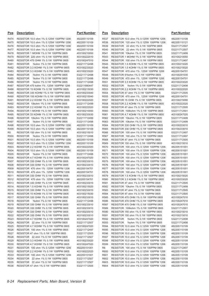
Pos Description Part Number
R474 RESISTOR 10.0 ohm 1% 0.125W 100PPM 1206 482205110109
R475 RESISTOR 10.0 ohm 1% 0.125W 100PPM 1206 482205110109
R476 RESISTOR 10.0 ohm 1% 0.125W 100PPM 1206 482205110109
R477 RESISTOR 10.0 ohm 1% 0.125W 100PPM 1206 482205110109
R478 RESISTOR 1 MOHM 1% 0.1W 100PPM 0805 403100210050
R479 RESISTOR 220 ohm 1% 0.1W 100PPM 0805 403100222010
R480 RESISTOR 470 OHM 1% 0.1W 100PPM 0805 403100247010
R481 RESISTOR 1kohm 1% 0.1W 100PPM 0805 532211712498
R482 RESISTOR 3.3 KOHM 1% 0.1W 100PPM 0805 403100233020
R483 RESISTOR 3.3 KOHM 1% 0.1W 100PPM 0805 403100233020
R484 RESISTOR 1kohm 1% 0.1W 100PPM 0805 532211712498
R485 RESISTOR 1kohm 1% 0.1W 100PPM 0805 532211712498
R486 RESISTOR 1kohm 1% 0.1W 100PPM 0805 532211712498
R487 RESISTOR 470 kohm 1% .125W 100PPM 1206 532211680447
R488 RESISTOR 15 KOHM 1% 0.1W 100PPM 0805 403100215030
R489 RESISTOR 330 KOHM 1% 0.1W 100PPM 0805 403100233040
R490 RESISTOR 150 KOHM 1% 0.1W 100PPM 0805 403100215040
R491 RESISTOR 2.2 KOHM 1% 0.1W 100PPM 0805 403100222020
R492 RESISTOR 10kohm 1% 0.1W 100PPM 0805 532211712499
R493 RESISTOR 2.2 KOHM 1% 0.1W 100PPM 0805 403100222020
R494 RESISTOR 1 MOHM 1% 0.1W 100PPM 0805 403100210050
R495 RESISTOR 33 KOHM 1% 0.1W 100PPM 0805 403100233030
R496 RESISTOR 10kohm 1% 0.1W 100PPM 0805 532211712499
R497 RESISTOR 1kohm 1% 0.1W 100PPM 0805 532211712498
R498 RESISTOR 10.0 ohm 1% 0.125W 100PPM 1206 482205110109
R499 RESISTOR 10.0 ohm 1% 0.125W 100PPM 1206 482205110109
R5 RESISTOR 150 ohm 1% 0.1W 100PPM 0805 403100215010
R500 RESISTOR 1kohm 1% 0.1W 100PPM 0805 532211712498
R501 RESISTOR 10.0 ohm 1% 0.125W 100PPM 1206 482205110109
R502 RESISTOR 10.0 ohm 1% 0.125W 100PPM 1206 482205110109
R503 RESISTOR 2.2 KOHM 1% 0.1W 100PPM 0805 403100222020
R504 RESISTOR 10.0 ohm 1% 0.125W 100PPM 1206 482205110109
R505 RESISTOR 1kohm 1% 0.1W 100PPM 0805 532211712498
R506 RESISTOR 4.7 KOHM 1% 0.1W 100PPM 0805 403100247020
R507 RESISTOR 330 OHM 1% 0.1W 100PPM 0805 403100233010
R508 RESISTOR 330 OHM 1% 0.1W 100PPM 0805 403100233010
R509 RESISTOR 470 ohm 1% .125W 100PPM 1206 482205154701
R510 RESISTOR 470 ohm 1% .125W 100PPM 1206 482205154701
R511 RESISTOR 330 OHM 1% 0.1W 100PPM 0805 403100233010
R512 RESISTOR 470 ohm 1% .125W 100PPM 1206 482205154701
R513 RESISTOR 330 OHM 1% 0.1W 100PPM 0805 403100233010
R514 RESISTOR 1.5 KOHM 1% 0.1W 100PPM 0805 403100215020
R515 RESISTOR 330 OHM 1% 0.1W 100PPM 0805 403100233010
R516 RESISTOR 15 KOHM 1% 0.1W 100PPM 0805 403100215030
R517 RESISTOR 330 OHM 1% 0.1W 100PPM 0805 403100233010
R518 RESISTOR 1kohm 1% 0.1W 100PPM 0805 532211712498
R519 RESISTOR 330 OHM 1% 0.1W 100PPM 0805 403100233010
R520 RESISTOR 330 OHM 1% 0.1W 100PPM 0805 403100233010
R521 RESISTOR 330 OHM 1% 0.1W 100PPM 0805 403100233010
R522 RESISTOR 330 OHM 1% 0.1W 100PPM 0805 403100233010
R523 RESISTOR 4.7 KOHM 1% 0.1W 100PPM 0805 403100247020
R524 RESISTOR 22 ohm 1% 0.1W 100PPM 0805 532211712507
R525 RESISTOR 4.7 KOHM 1% 0.1W 100PPM 0805 403100247020
R526 RESISTOR 100 ohm 1% 0.1W 100PPM 0805 532211712497
R527 RESISTOR 47 ohm 1% 0.1W 100PPM 0805 532211712505
R528 RESISTOR 22 ohm 1% 0.1W 100PPM 0805 532211712507
R529 RESISTOR 3.3 KOHM 1% 0.1W 100PPM 0805 403100233020
R530 RESISTOR 4.7 KOHM 1% 0.1W 100PPM 0805 403100247020
R531 RESISTOR 100 ohm 1% 0.125W 100PPM 1206 482205151001
R532 RESISTOR 2.2 KOHM 1% 0.1W 100PPM 0805 403100222020
R533 RESISTOR 100 ohm 1% 0.125W 100PPM 1206 482205151001
R534 RESISTOR 22 ohm 1% 0.1W 100PPM 0805 532211712507
R535 RESISTOR 22 ohm 1% 0.1W 100PPM 0805 532211712507
R536 RESISTOR 47 ohm 1% 0.1W 100PPM 0805 532211712505
Pos Description Part Number
R537 RESISTOR 10.0 ohm 1% 0.125W 100PPM 1206 482205110109
R538 RESISTOR 120 ohm 1% 0.125W 100PPM 1206 482205110121
R539 RESISTOR 22 ohm 1% 0.1W 100PPM 0805 532211712507
R540 RESISTOR 22 ohm 1% 0.1W 100PPM 0805 532211712507
R541 RESISTOR 10kohm 1% 0.1W 100PPM 0805 532211712499
R543 RESISTOR 1 MOHM 1% 0.1W 100PPM 0805 403100210050
R544 RESISTOR 100 ohm 1% 0.1W 100PPM 0805 532211712497
R545 RESISTOR 1.5 KOHM 1% 0.1W 100PPM 0805 403100215020
R546 RESISTOR 1.5 KOHM 1% 0.1W 100PPM 0805 403100215020
R547 RESISTOR 470 ohm 1% .125W 100PPM 1206 482205154701
R548 RESISTOR 91kohm 1% 0.1W 100PPM 0805 403100291030
R549 RESISTOR 470 ohm 1% .125W 100PPM 1206 482205154701
R551 RESISTOR 3.3 KOHM 1% 0.1W 100PPM 0805 403100233020
R552 RESISTOR 1kohm 1% 0.1W 100PPM 0805 532211712498
R553 RESISTOR 2.2 KOHM 1% 0.1W 100PPM 0805 403100222020
R554 RESISTOR 47 ohm 1% 0.1W 100PPM 0805 532211712505
R555 RESISTOR 470 ohm 1% .125W 100PPM 1206 482205154701
R557 RESISTOR 15 OHM 1% 0.1W 100PPM 0805 403100215090
R558 RESISTOR 2.2 KOHM 1% 0.1W 100PPM 0805 403100222020
R559 RESISTOR 47 ohm 1% 0.1W 100PPM 0805 532211712505
R560 RESISTOR 100kohm 1% 0.1W 100PPM 0805 532211712501
R561 RESISTOR 4.7 KOHM 1% 0.1W 100PPM 0805 403100247020
R562 RESISTOR 10kohm 1% 0.1W 100PPM 0805 532211712499
R563 RESISTOR 10kohm 1% 0.1W 100PPM 0805 532211712499
R564 RESISTOR 330 OHM 1% 0.1W 100PPM 0805 403100233010
R565 RESISTOR 330 OHM 1% 0.1W 100PPM 0805 403100233010
R566 RESISTOR 100 ohm 1% 0.1W 100PPM 0805 532211712497
R567 RESISTOR 100 ohm 1% 0.1W 100PPM 0805 532211712497
R568 RESISTOR 47 ohm 1% 0.1W 100PPM 0805 532211712505
R569 RESISTOR 150 ohm 1% 0.1W 100PPM 0805 403100215010
R570 RESISTOR 100 ohm 1% 0.125W 100PPM 1206 482205151001
R571 RESISTOR 100 ohm 1% 0.125W 100PPM 1206 482205151001
R572 RESISTOR 100 ohm 1% 0.125W 100PPM 1206 482205151001
R573 RESISTOR 100 ohm 1% 0.125W 100PPM 1206 482205151001
R575 RESISTOR 100 ohm 1% 0.125W 100PPM 1206 482205151001
R576 RESISTOR 100 ohm 1% 0.125W 100PPM 1206 482205151001
R577 RESISTOR 100 ohm 1% 0.125W 100PPM 1206 482205151001
R578 RESISTOR 100 ohm 1% 0.125W 100PPM 1206 482205151001
R579 RESISTOR 1.5 KOHM 1% 0.1W 100PPM 0805 403100215020
R580 RESISTOR 3.3 KOHM 1% 0.1W 100PPM 0805 403100233020
R581 RESISTOR 47 ohm 1% 0.1W 100PPM 0805 532211712505
R582 RESISTOR 10kohm 1% 0.1W 100PPM 0805 532211712499
R583 RESISTOR 47 ohm 1% 0.1W 100PPM 0805 532211712505
R584 RESISTOR 47 ohm 1% 0.1W 100PPM 0805 532211712505
R585 RESISTOR 470 OHM 1% 0.1W 100PPM 0805 403100247010
R586 RESISTOR 470 OHM 1% 0.1W 100PPM 0805 403100247010
R587 RESISTOR 470 OHM 1% 0.1W 100PPM 0805 403100247010
R589 RESISTOR 100kohm 1% 0.1W 100PPM 0805 532211712501
R590 RESISTOR 150 ohm 1% 0.1W 100PPM 0805 403100215010
R591 RESISTOR 150 ohm 1% 0.1W 100PPM 0805 403100215010
R592 RESISTOR 1kohm 1% 0.1W 100PPM 0805 532211712498
R593 RESISTOR 1kohm 1% 0.1W 100PPM 0805 532211712498
R594 RESISTOR 10.0 ohm 1% 0.125W 100PPM 1206 482205110109
R595 RESISTOR 10.0 ohm 1% 0.125W 100PPM 1206 482205110109
R596 RESISTOR 10.0 ohm 1% 0.125W 100PPM 1206 482205110109
R597 RESISTOR 10.0 ohm 1% 0.125W 100PPM 1206 482205110109
R598 RESISTOR 10.0 ohm 1% 0.125W 100PPM 1206 482205110109
R599 RESISTOR 10.0 ohm 1% 0.125W 100PPM 1206 482205110109
R6 RESISTOR 100 ohm 1% 0.1W 100PPM 0805 532211712497
R600 RESISTOR 10.0 ohm 1% 0.125W 100PPM 1206 482205110109
R601 RESISTOR 10.0 ohm 1% 0.125W 100PPM 1206 482205110109
R602 RESISTOR 10.0 ohm 1% 0.125W 100PPM 1206 482205110109
R603 RESISTOR 10.0 ohm 1% 0.125W 100PPM 1206 482205110109
R604 RESISTOR 10.0 ohm 1% 0.125W 100PPM 1206 482205110109
8-24 Replacement Parts, Main Board, Version B
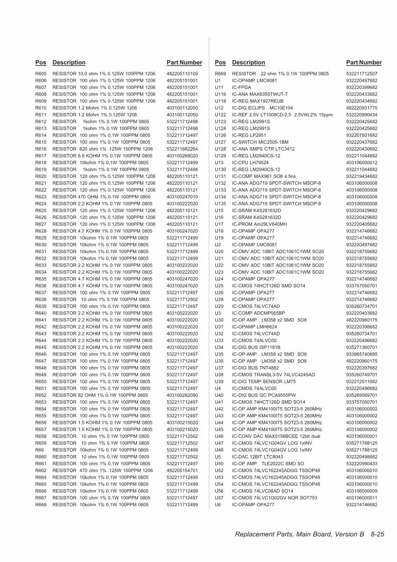
Pos Description Part Number
R605 RESISTOR 10.0 ohm 1% 0.125W 100PPM 1206 482205110109
R606 RESISTOR 100 ohm 1% 0.125W 100PPM 1206 482205151001
R607 RESISTOR 100 ohm 1% 0.125W 100PPM 1206 482205151001
R608 RESISTOR 100 ohm 1% 0.125W 100PPM 1206 482205151001
R609 RESISTOR 100 ohm 1% 0.125W 100PPM 1206 482205151001
R610 RESISTOR 1.2 Mohm 1% 0.125W 1206 403100112050
R611 RESISTOR 1.2 Mohm 1% 0.125W 1206 403100112050
R612 RESISTOR 1kohm 1% 0.1W 100PPM 0805 532211712498
R613 RESISTOR 1kohm 1% 0.1W 100PPM 0805 532211712498
R614 RESISTOR 100 ohm 1% 0.1W 100PPM 0805 532211712497
R615 RESISTOR 100 ohm 1% 0.1W 100PPM 0805 532211712497
R616 RESISTOR 820 ohm 1% .125W 100PPM 1206 532211682264
R617 RESISTOR 6.8 KOHM 1% 0.1W 100PPM 0805 403100268020
R618 RESISTOR 10kohm 1% 0.1W 100PPM 0805 532211712499
R619 RESISTOR 1kohm 1% 0.1W 100PPM 0805 532211712498
R620 RESISTOR 120 ohm 1% 0.125W 100PPM 1206 482205110121
R621 RESISTOR 120 ohm 1% 0.125W 100PPM 1206 482205110121
R622 RESISTOR 120 ohm 1% 0.125W 100PPM 1206 482205110121
R623 RESISTOR 470 OHM 1% 0.1W 100PPM 0805 403100247010
R624 RESISTOR 2.2 KOHM 1% 0.1W 100PPM 0805 403100222020
R625 RESISTOR 120 ohm 1% 0.125W 100PPM 1206 482205110121
R626 RESISTOR 120 ohm 1% 0.125W 100PPM 1206 482205110121
R627 RESISTOR 120 ohm 1% 0.125W 100PPM 1206 482205110121
R628 RESISTOR 4.7 KOHM 1% 0.1W 100PPM 0805 403100247020
R629 RESISTOR 10kohm 1% 0.1W 100PPM 0805 532211712499
R630 RESISTOR 10kohm 1% 0.1W 100PPM 0805 532211712499
R631 RESISTOR 10kohm 1% 0.1W 100PPM 0805 532211712499
R632 RESISTOR 10kohm 1% 0.1W 100PPM 0805 532211712499
R633 RESISTOR 2.2 KOHM 1% 0.1W 100PPM 0805 403100222020
R634 RESISTOR 2.2 KOHM 1% 0.1W 100PPM 0805 403100222020
R635 RESISTOR 4.7 KOHM 1% 0.1W 100PPM 0805 403100247020
R636 RESISTOR 4.7 KOHM 1% 0.1W 100PPM 0805 403100247020
R637 RESISTOR 100 ohm 1% 0.1W 100PPM 0805 532211712497
R638 RESISTOR 10 ohm 1% 0.1W 100PPM 0805 532211712502
R639 RESISTOR 100 ohm 1% 0.1W 100PPM 0805 532211712497
R640 RESISTOR 2.2 KOHM 1% 0.1W 100PPM 0805 403100222020
R641 RESISTOR 2.2 KOHM 1% 0.1W 100PPM 0805 403100222020
R642 RESISTOR 2.2 KOHM 1% 0.1W 100PPM 0805 403100222020
R643 RESISTOR 2.2 KOHM 1% 0.1W 100PPM 0805 403100222020
R644 RESISTOR 2.2 KOHM 1% 0.1W 100PPM 0805 403100222020
R645 RESISTOR 2.2 KOHM 1% 0.1W 100PPM 0805 403100222020
R646 RESISTOR 100 ohm 1% 0.1W 100PPM 0805 532211712497
R647 RESISTOR 100 ohm 1% 0.1W 100PPM 0805 532211712497
R648 RESISTOR 100 ohm 1% 0.1W 100PPM 0805 532211712497
R649 RESISTOR 100 ohm 1% 0.1W 100PPM 0805 532211712497
R650 RESISTOR 100 ohm 1% 0.1W 100PPM 0805 532211712497
R651 RESISTOR 100 ohm 1% 0.1W 100PPM 0805 532211712497
R652 RESISTOR 82 OHM 1% 0.1W 100PPM 0805 403100282090
R653 RESISTOR 100 ohm 1% 0.1W 100PPM 0805 532211712497
R654 RESISTOR 100 ohm 1% 0.1W 100PPM 0805 532211712497
R655 RESISTOR 100 ohm 1% 0.1W 100PPM 0805 532211712497
R656 RESISTOR 1.5 KOHM 1% 0.1W 100PPM 0805 403100215020
R657 RESISTOR 1.5 KOHM 1% 0.1W 100PPM 0805 403100215020
R658 RESISTOR 10 ohm 1% 0.1W 100PPM 0805 532211712502
R659 RESISTOR 10 ohm 1% 0.1W 100PPM 0805 532211712502
R66 RESISTOR 10kohm 1% 0.1W 100PPM 0805 532211712499
R660 RESISTOR 10 ohm 1% 0.1W 100PPM 0805 532211712502
R661 RESISTOR 100 ohm 1% 0.1W 100PPM 0805 532211712497
R662 RESISTOR 470 ohm 1% .125W 100PPM 1206 482205154701
R664 RESISTOR 10kohm 1% 0.1W 100PPM 0805 532211712499
R665 RESISTOR 10kohm 1% 0.1W 100PPM 0805 532211712499
R666 RESISTOR 10kohm 1% 0.1W 100PPM 0805 532211712499
R667 RESISTOR 100 ohm 1% 0.1W 100PPM 0805 532211712497
R668 RESISTOR 10kohm 1% 0.1W 100PPM 0805 532211712499
Pos Description Part Number
R669 RESISTOR 22 ohm 1% 0.1W 100PPM 0805 532211712507
U1 IC-OPAMP LMC6081 932220497682
U11 IC-FPGA 932220399682
U116 IC-ANA MAX6355TWUT-T 932220433682
U118 IC-REG MAX1927REUB 932220434682
U12 IC-DIG ECLIPS MC10E104 482220931775
U122 IC-REF 2.5V LT1009CD-2.5 2.5Vñ0.2% 15ppm 532220990434
U123 IC-REG LM2991S 932220425682
U124 IC-REG LM2991S 932220425682
U126 IC-REG LP2951 932207501682
U127 IC-SWITCH MIC2505-1BM 932220437682
U128 IC-ANA SMPS CTR LTC3412 932220430682
U129 IC-REG LM2940CS-12 932211044682
U13 IC-CPU LH79524 403106000012
U130 IC-REG LM2940CS-12 932211044682
U131 IC-COMP MAX961 SO8 4.5ns 932219434682
U132 IC-ANA ADG719 SPDT-SWITCH MSOP-8 403106000008
U133 IC-ANA ADG719 SPDT-SWITCH MSOP-8 403106000008
U134 IC-ANA ADG719 SPDT-SWITCH MSOP-8 403106000008
U135 IC-ANA ADG719 SPDT-SWITCH MSOP-8 403106000008
U15 IC-SRAM K4S281632D 932220429682
U16 IC-SRAM K4S281632D 932220429682
U17 IC-PROM Am29LV640MH 932220405682
U18 IC-OPAMP OPA277 932214746682
U19 IC-OPAMP OPA277 932214746682
U2 IC-OPAMP LMC6081 932220497682
U20 IC-OMV ADC 10BIT ADC1061C1WM SO20 932218755682
U21 IC-OMV ADC 10BIT ADC1061C1WM SO20 932218755682
U22 IC-OMV ADC 10BIT ADC1061C1WM SO20 932218755682
U23 IC-OMV ADC 10BIT ADC1061C1WM SO20 932218755682
U24 IC-OPAMP OPA277 932214746682
U25 IC-CMOS 74HCT126D SMD SO14 933757050701
U26 IC-OPAMP OPA277 932214746682
U28 IC-OPAMP OPA277 932214746682
U29 IC-CMOS 74LVC74AD 935260734701
U3 IC-COMP ADCMP565BP 932220403682
U30 IC-OP AMP LM358 x2 SMD SO8 482220960175
U31 IC-OPAMP LMH6624 932220398682
U32 IC-CMOS 74LVC74AD 935260734701
U33 IC-CMOS 74ALVC00 932220496682
U34 IC-DIG BUS ISP1181B 935271360701
U35 IC-OP AMP LM358 x2 SMD SO8 933965740685
U35 IC-OP AMP LM358 x2 SMD SO8 482220960175
U37 IC-DIG BUS TNT4882 932220397682
U38 IC-CMOS TRANSL3-5V 74LVC4245AD 935260749701
U39 IC-DIG TEMP SENSOR LM75 932212511682
U4 IC-CMOS 74ALVC00 932220496682
U40 IC-DIG BUS I2C PCA9555PW 935269569701
U41 IC-CMOS 74HCT126D SMD SO14 933757050701
U42 IC-OP AMP KM4100IT5 SOT23-5 260MHz 403106000002
U43 IC-OP AMP KM4100IT5 SOT23-5 260MHz 403106000002
U44 IC-OP AMP KM4100IT5 SOT23-5 260MHz 403106000002
U45 IC-OP AMP KM4100IT5 SOT23-5 260MHz 403106000002
U46 IC-CONV DAC MAX5156BCEE 12bit dual 403106000001
U47 IC-CMOS 74LVC1G04GV LOG 1xINV 935271788125
U48 IC-CMOS 74LVC1G04GV LOG 1xINV 935271788125
U5 IC-DAC 12BIT LTC8043 932220498682
U50 IC-OP AMP TLE2022C SMD SO 532220990433
U52 IC-CMOS 74LVC162245ADGG TSSOP48 403106000010
U53 IC-CMOS 74LVC162245ADGG TSSOP48 403106000010
U54 IC-CMOS 74LVC162245ADGG TSSOP48 403106000010
U56 IC-CMOS 74LVC08AD SO14 403106000009
U57 IC-CMOS 74LVC1G02GV NOR SOT753 403106000011
U6 IC-OPAMP OPA277 932214746682
Replacement Parts, Main Board, Version B 8-25
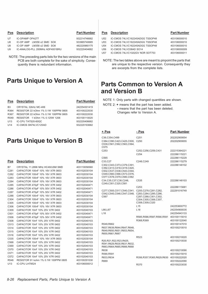
Pos Description Part Number
U7 IC-OPAMP OPA277 932214746682
U8 IC-OP AMP LM358 x2 SMD SO8 933965740685
U8 IC-OP AMP LM358 x2 SMD SO8 482220960175
U9 IC-ANALOG-PLL 200MHz ADF4001BRU 932220404682
NOTE: The preceding parts lists for the two versions of the main
PCB are both complete for the sake of simplicity. Conse-
quently there is redundant information.
Parts Unique to Version A
Pos Description Part Number
B3 CRYSTAL 32kHz MC-406 242254301419
R364 RESISTOR 22 kOhm 1% 0.1W 100PPM 0805 403100222030
R367 RESISTOR 22 kOhm 1% 0.1W 100PPM 0805 403100222030
R549 RESISTOR 1 kOhm 1% 0.125W 1206 403100110020
U13 IC-CPU TA7S20-60QC 932220406682
U14 IC-CMOS SN74LVC125AD 932220193682
Parts Unique to Version B
Pos Description Part Number
B7 CRYSTAL 11.2896 MHz HC49/USM SMD 403110056560
C281 CAPACITOR 100nF 10% 16V X7R 0603 403102030104
C282 CAPACITOR 100nF 10% 16V X7R 0603 403102030104
C283 CAPACITOR 100nF 10% 16V X7R 0603 403102030104
C284 CAPACITOR 100nF 10% 16V X7R 0603 403102030104
C285 CAPACITOR 470pF 10% 50V X7R 0402 403102040471
C286 CAPACITOR 470pF 10% 50V X7R 0402 403102040471
C287 CAPACITOR 470pF 10% 50V X7R 0402 403102040471
C288 CAPACITOR 100nF 10% 16V X7R 0603 403102030104
C304 CAPACITOR 100nF 10% 16V X7R 0603 403102030104
C305 CAPACITOR 100nF 10% 16V X7R 0603 403102030104
C306 CAPACITOR 100nF 10% 16V X7R 0603 403102030104
C309 CAPACITOR 10nF 10% 25V X7R 0402 403102040103
C501 CAPACITOR 470pF 10% 50V X7R 0402 403102040471
C506 CAPACITOR 470pF 10% 50V X7R 0402 403102040471
C508 CAPACITOR 10nF 10% 25V X7R 0402 403102040103
C513 CAPACITOR 10nF 10% 25V X7R 0402 403102040103
C514 CAPACITOR 10nF 10% 25V X7R 0402 403102040103
C515 CAPACITOR 10nF 10% 25V X7R 0402 403102040103
C516 CAPACITOR 10nF 10% 25V X7R 0402 403102040103
C535 CAPACITOR 100nF 10% 16V X7R 0603 403102030104
C568 CAPACITOR 10nF 10% 25V X7R 0402 403102040103
C569 CAPACITOR 10nF 10% 25V X7R 0402 403102040103
C570 CAPACITOR 10nF 10% 25V X7R 0402 403102040103
C571 CAPACITOR 10nF 10% 25V X7R 0402 403102040103
C572 CAPACITOR 10nF 10% 25V X7R 0402 403102040103
R548 RESISTOR 91 kohm 1% 0.1W 100PPM 0805 403100291030
U13 IC-CPU LH79524 403106000012
Pos Description Part Number
U52 IC-CMOS 74LVC162245ADGG TSSOP48 403106000010
U53 IC-CMOS 74LVC162245ADGG TSSOP48 403106000010
U54 IC-CMOS 74LVC162245ADGG TSSOP48 403106000010
U56 IC-CMOS 74LVC08AD SO14 403106000009
U57 IC-CMOS 74LVC1G02GV NOR SOT753 403106000011
NOTE: The two tables above are meant to pinpoint the parts that
are unique to the respective version. Consequently they
are excerpts from the complete lists.
Parts Common to Version Aand Version B
NOTE 1: Only parts with changed quantities are shown.
NOTE 2: + means that the part has been added.
- means that the part has been deleted.
Changes refer to Version A.
+ Pos - Pos Part Number
C36,C354,C499 C251 202202900654
C384,C390,C423,C425,C500,
C539,C561,C562,C563,C564,
C575
C250 202202900655
C253 C252,C256,C259,C431 222215364221
C254 222286115221
C565 222286115229
C33,C27 C248,C249 222286115279
C302,C343,C373,C379,C391,
C392,C413,C418,C419,C420,
C502,C537,C538,C543,C544,
C549,C560,C566,C573,C576,
C577,C578,C579,C580,C582
222286148102
C34,C35,C37,C38,C248,
C249,C301,C320,C581
C535 222286148103
C253 222286115681
C277,C505,C517,C540,C541,
C542,C545,C546,C547,C548,
C567
C255,C278,C281,C282,
C283,C284,C285,C286,
C287,C288,C301,C302,
C304,C305,C306,C307,
C308,C309,C320
222291016749
L15 242253600772
L66,L67 L18 242254900035
L18 242254943133
R585,R586,R587,R590,R591 403100115010
R368,R369 403100122040
R549,R662 403100147010
R637,R639,R644,R647,R648,
R649,R650,R651,R653,R654,
R655,R661,R667
403100210010
R523 403100210020
R20,R21,R22,R23,R425,
R541,R629,R630,R631,R632,
R663,R664,R665,R666,R668
403100210030
R638 403100210090
R590,R591 403100215010
R633,R634 R356,R357,R365,R629,R630 403100222020
R669 403100222090
R370 403100233030
8-26 Replacement Parts, Parts Unique to Version A
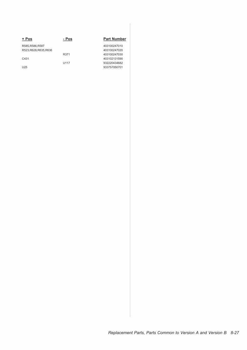
+ Pos - Pos Part Number
R585,R586,R587 403100247010
R523,R628,R635,R636 403100247020
R371 403100247030
C431 403102131590
U117 932220434682
U25 933757050701
Replacement Parts, Parts Common to Version A and Version B 8-27
This page is intentionally left blank.
8-28 Replacement Parts, Parts Common to Version A and Version B

Chapter 9
Schematic Diagrams
How to Read the Diagrams
This chapter contains circuit diagrams and component layout
information.
Signals
The signal designations reflect the functions. ADCDATA0,
for instance, means DATA BIT 0 from the ADC (Analog/Dig-
ital Converter).
Three different types of graphic symbols are used to mark ref-
erences for continued connection somewhere else in the dia-
gram.
This arrow is used if the reference to a supply
voltage is directed to a point located on the same
sheet. The example means that the supply voltage
-2.1V can also be found elsewhere on the same sheet.
This arrow is used if the reference to a supply
voltage or a signal is directed to a point located
on another sheet. The example means that the
supply voltage +3.3VD goes to sheet 1, 2, 5, 7 and 8.
A broken line with a signal designation label
means that this particular signal can also be
found elsewhere on the same sheet.
Circuit Symbols
The diagrams are computer-drawn. The symbols conform to
IEC standards. These symbols are designed to be logical and
easy to read.
The component number is written above the symbol. The type
number is written below the symbol
Inside the symbol there is sometimes an abbreviated descrip-
tion of the circuit’s function.
Pin numbers are written outside the symbol and, if the circuit
is complex, the pin functions are written inside.
A small circle on a pin indicates that the input/output inverts
the signal.
The signal flow through the circuit is normally from left to
right.
Resistors, Capacitors, Diodes,Transistors and Other Components.
These components are similar to the old-fashioned,
hand-drawn symbols. They have their component numbers
above or beside the symbol and their value or type number be-
low the component number.
Component Numbers
Letters Components
B Crystals and crystal filters
C Capacitors
D Diodes
F Fuses
J Jumpers and connectors
K Relays
L Coils
P Connectors
Q Transistors
R Resistors
U ICs
X Test points
The numbers that follow are sequential and serve as sche-
matic diagram and layout identifiers together with the leading
character.
9-2 Schematic Diagrams
-2.1V
+3.3VD 1,2,5,7,8
PLL LOCK
Version A
The descriptions in this section apply to instru-
ments having a Triscend microprocessor.
See General Information on page III for details on
relevant serial numbers etc.
Schematic Diagrams 9-3

This page is intentionally left blank.
9-4 Schematic Diagrams

This page is intentionally left blank.
Schematic Diagrams 9-5
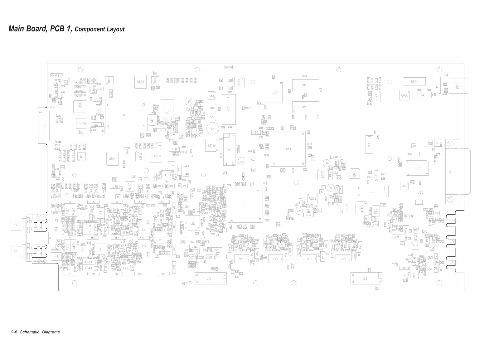
Main Board, PCB 1, Component Layout
9-6 Schematic Diagrams
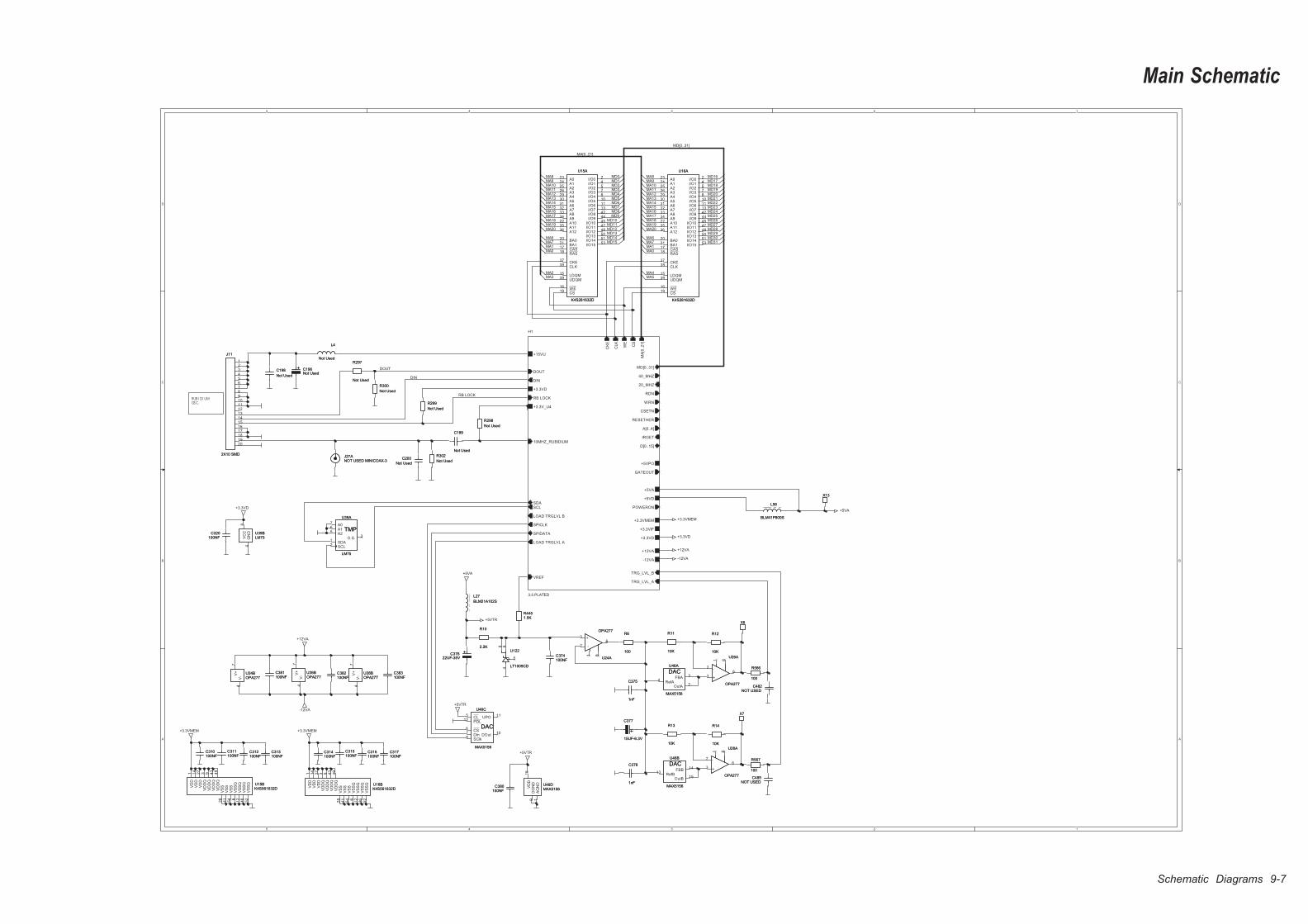
Main Schematic
Schematic Diagrams 9-7
5
5
4
4
3
3
2
2
1
1
D D
C C
B B
A A
DOUT
MD9MD10MD11MD12MD13MD14MD15
MA8MA9MA10MA11MA12MA13MA14MA15MA16MA17MA18MA19MA20
MA6MA7
MA8
MA1MA0
MA2
MA9
MA3
MA10MA11MA12MA13MA14MA15MA16MA17MA18MA19MA20
MA6MA7MA1
MA4
MA0
MA5
MD16MD17MD18MD19MD20MD21MD22MD23MD24MD25MD26MD27MD28MD29MD30MD31
MD0MD1MD2MD3MD4MD5MD6MD7MD8
DIN
RB LOCK
MD[0..31]
MA[0..21]
+5VTR
+3.3VMEM
+5VA
+3.3VD
+12VA
-12VA
+5VTR
+3.3VMEM+3.3VMEM
+5VA
+3.3VD
+12VA
-12VA
+5VTR
RUBI DI UMOSC.
L56
BLM41P800S
L56
BLM41P800S
X7X7
46
5
8
U122
LT1009CD
U122
LT1009CD
C315100NFC315100NF
C375
1nF
C375
1nF
C381100NFC381100NF
C377
15UF-6.3V
C377
15UF-6.3V
R297
Not Used
R297
Not Used
L4
Not Used
L4
Not Used
R11
10K
R11
10K
C311100NFC311100NF
L27
BLM21A102S
L27
BLM21A102S
R10
2.2K
R10
2.2K
C380100NF
C380100NF
V+
7
V-
4
U26BOPA277U26BOPA277
C196Not UsedC196Not Used
VD
D1
VD
D1
4
VD
D2
7
VD
DQ
3
VD
DQ
9
VD
DQ
43
VD
DQ
49
VS
S2
8
VS
S4
1
VS
S5
4
VS
SQ
6
VS
SQ
12
VS
SQ
46
VS
SQ
52
U15BK4S561632DU15BK4S561632D
X13X13
RefA4
FBA3
OutA2
DACU46A
MAX5156
DACU46A
MAX5156
3
26
1 8
-
+
U28A
OPA277
-
+
U28A
OPA277
C198
Not Used
C198
Not Used
J27ANOT USED MINICOAX-3J27ANOT USED MINICOAX-3
R298
Not Used
R298
Not Used
R4451.5KR4451.5K
C485NOT USED
C485NOT USED
A023
A124
A225
A326
A429
A530
A631
A732
A833
A934
A1022
A1135
A1236
I/O02
I/O14
I/O25
I/O37
I/O48
I/O510
I/O611
I/O713
I/O842
I/O944
I/O1045
I/O1147
I/O1248
I/O1350
I/O1451
I/O1553
RAS18
WE16
CS19
CAS17
LDQM15
BA020
BA121
UDQM39
CKE37
CLK38
U15A
K4S281632D
U15A
K4S281632D
1234567891011121314151617181920
J11
2X10 SMD
J11
2X10 SMD
C310100NFC310100NF
C383100NFC383100NF
VD
D1
VD
D1
4
VD
D2
7
VD
DQ
3
VD
DQ
9
VD
DQ
43
VD
DQ
49
VS
S2
8
VS
S4
1
VS
S5
4
VS
SQ
6
VS
SQ
12
VS
SQ
46
VS
SQ
52
U16BK4S561632DU16BK4S561632D
C378
1nF
C378
1nF
R6
100
R6
100
R13
10K
R13
10K
A023
A124
A225
A326
A429
A530
A631
A732
A833
A934
A1022
A1135
A1236
I/O02
I/O14
I/O25
I/O37
I/O48
I/O510
I/O611
I/O713
I/O842
I/O944
I/O1045
I/O1147
I/O1248
I/O1350
I/O1451
I/O1553
RAS18
WE16
CS19
CAS17
LDQM15
BA020
BA121
UDQM39
CKE37
CLK38
U16A
K4S281632D
U16A
K4S281632D
R299
Not Used
R299
Not Used
C200
Not Used
C200
Not Used
R12
10K
R12
10K
C320100NF
C320100NF
R567
100
R567
100
C312100NFC312100NF
V+
7
V-
4
U28BOPA277U28BOPA277
SDA1
SCL2
A07
A16
A25
O.S.3
TMP
U39A
LM75
TMP
U39A
LM75
H1
3.5 PLATED
SDASCL
10MHZ_RUBIDIUM
RB LOCK
DIN
DOUT
+15VU
MA
[0..2
1]
MD[0..31]
CS
WE
CL
K
CK
E
LOAD TRGLVL A
LOAD TRGLVL B
SPICLK
SPIDATA
VREFTRG_LVL_A
TRG_LVL_B
RDN
WRN
RESETHER
CSETN
A[0..4]
D[0..15]
40_MHZ
IRGET
GATEOUT
+5VPO
+3.3VMEM
+3.3VIF
+3.3V_U4
+3.3VD
+5VD
+5VA
POWERON
+3.3VD
+12VA
-12VA
20_MHZ
GN
D4
VC
C8
U39BLM75U39BLM75
UPO11
DOut10
PDL12
CL5
CS6
DIn7
SClk8
DAC
U46C
MAX5156
DAC
U46C
MAX5156
C313100NFC313100NF
C374100NFC374100NF
C37622UF-35V
C37622UF-35V
R566
100
R566
100
R302
Not Used
R302
Not Used
X6X6
C382100NFC382100NF 3
26
1 8
-
+
U26A
OPA277
-
+
U26A
OPA277
C199
Not Used
C199
Not Used
VD
D1
6
DG
ND
9
AG
ND
1
U46DMAX5156U46DMAX5156
RefB13
FBB14
OutB15
DACU46B
MAX5156
DACU46B
MAX5156
C316100NFC316100NF
R300
Not Used
R300
Not Used
3
26
1 8
-
+
U24A
OPA277
-
+
U24A
OPA277
C482NOT USED
C482NOT USED
R14
10K
R14
10K
C317100NFC317100NF
V+
7
V-
4
U24BOPA277U24BOPA277
C314100NFC314100NF

9-8 Schematic Diagrams
This page is intentionally left blank.
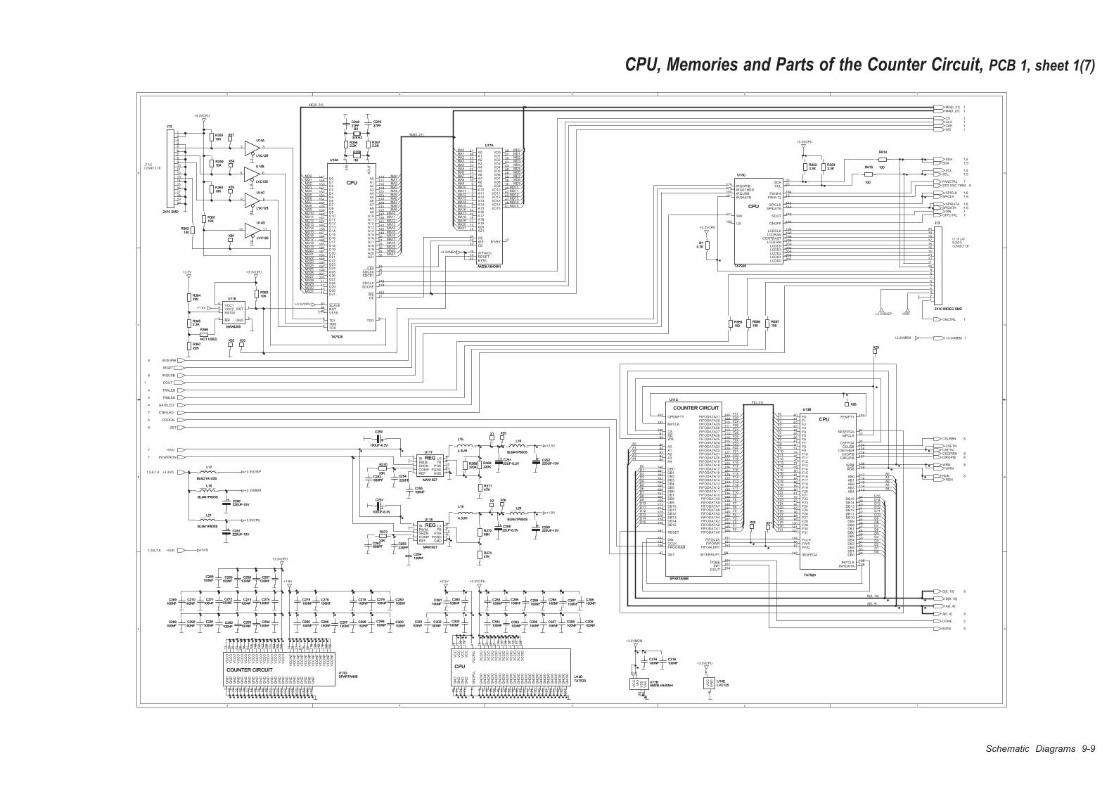
CPU, Memories and Parts of the Counter Circuit, PCB 1, sheet 1(7)
Schematic Diagrams 9-9
5
5
4
4
3
3
2
2
1
1
D D
C C
B B
A A
F16
D4
D14
F6
F10
F22
D6
A0
F28
F24
D10D9
F17
F31
F0
F11
D3
F7
F23
D13
A4
F8
F3
F29
D5
F2
F25
F18
D[0..15]
D8 F9
F1
F12
F14
A3
D2
A[0..4]
D12F4
F26
F19
A2
F15D1
F[0..31]
D15
D7
F21
F5
D0
A1
F30
D11
F13
F27
F20
A0A1A2A3A4
D15D14D13D12D11D10D9D8D7D6D5D4D3D2D1D0
F0F1F2F3F4F5F6F7F8F9F10F11F12F13F14F15F16F17F18F19F20F21F22F23F24F25F26F27F28F29F30F31
MD10
MD[0..31]
MD0
MD12
MD25
MD23
MA5MA13
MD2MA1
MD29
MA12
MA21MA20
MA4
MD15
MA18
MD8
MD16
MD1
MA15
MD1MA2
MD19
MD22
MD18
MD8
MA4
MA11
MD9
MA21
MA[0..21]
MD0
MA3
MA0
MA9
MA19
MD21
MA13
MD30
MA17
MD4
MD26
MD14
MA8
MD31
MA17
MA6
MD15MD7
MD13
MD3
MD20
MA7MD6
MA8
MD10MD2
MD27
MA20
MA7
MA0
MD5
MD24
MD11MA10
MA16
MA1
MA14
MA6
MA16
MA3MA2
MD17
MD28
MD13
MA15
MD12MD11
MA14
MA19
MD7
MA9
MD5
MA18
MA5MD6
MD14
MD4
MA11MA12
MD3
MD9MA10
SDA 1,5
SCL 1,5
CS 1CLK 1CKE 1WE 1
DIN 1
DOUT1
MA[0..21] 1MD[0..31] 1
A[0..4]
D[0..15]
WRN
RDN
CSETN
+3.3VMEM 1
IRGET
SPIDATA 1,6
SPICLK 1,6
+2.5V
+1.8V
+3.3VMEM
+3.3VCPU
+3.3VDISP
+5VD
+3.3VCPU
+3.3VCPU
+3.3VMEM
+3.3VCPU+2.5V+1.8V
+3.3VCPU
+3.3VCPU
+3.3VCPU
+1.8V
+2.5V
+5VD+3.3VDISP
+3.3VCPU
+3.3VCPU
+3.3VMEM
+3.3VMEM
POWERON7
+5VU7
GET8
PROGN5
IRQUSB8
IRQGPIB8
+3.3VD1,5,6,7,8
TRALED4
TRBLED4
GATELED4
STBYLED7
+5VD1,5,6,7,8
SDA 1,5
SCL 1,5
FANCTRL 7STD OSC TRIM 6
SPICLK 1,6
OFFCTRL 7
SPIDATA 1,6
RDN 8
DONE 5
INITN 5
CSGPIBN 8
CSUSBN 8
DIRGPIB 8
CSETN
WRN 8
ONCTRL 7
A[0..4] 8
D[0..15] 8
J T AGCONNECT OR
DI SPL AYBOARDCONNECT OR
C268100NF
C268100NF
5 6
4
U14B
LVC125
U14B
LVC125
FIFODATA31108
FIFODATA30109
FIFODATA29110
FIFODATA28111
FIFODATA27112
FIFODATA26113
FIFODATA25114
FIFODATA24115
FIFODATA23116
FIFODATA22120
FIFODATA21121
FIFODATA20122
FIFODATA19123
FIFODATA18125
FIFODATA17126
FIFODATA16127
FIFODATA15129
FIFODATA14132
FIFODATA13133
FIFODATA12134
FIFODATA11135
FIFODATA10136
FIFODATA9138
FIFODATA8139
FIFODATA7140
FIFODATA6141
FIFODATA5145
FIFODATA4146
FIFODATA3147
FIFODATA2148
FIFODATA1149
FIFODATA0150
FIFOCLK101
FIFOWR151
FIFOALERT152
UPEMPTY102
INTERRUPT99
MPCLK182
CS180
RD97
WR98
A088
A189
A293
A394
A495
DB0160
DB1161
DB2162
DB3163
DB4164
DB5165
DB6166
DB7167
DB8168
DB9169
DB10173
DB11174
DB12175
DB13176
DB14178
DB15179
RESET187
DIN153
CCLK155
PROGRAM106
DONE104
INIT107
GET87
DOUT154
COUNTER CIRCUIT
U11C
SPARTANIIE
COUNTER CIRCUIT
U11C
SPARTANIIE
C299100NFC299100NF
C264100NFC264100NF
C250
100UF-6.3V
C250
100UF-6.3V
C303100NF
C303100NF
R369220KR369220K
C25822UF-6.3VC25822UF-6.3V
X30X30
L21
BLM41P800S
L21
BLM41P800S
R3652.2KR3652.2K
R370
33K
R370
33K
C272100NF
C272100NF
F060
F161
F262
F363
F464
F565
F666
F767
F870
F971
F1074
F1175
F1276
F1377
F1479
F1580
F1681
F1785
F1886
F1989
F2090
F2191
F2292
F2393
F2494
F2595
F2696
F2798
F2899
F29100
F30101
F31102
FEMPTY103
FFIQ57
FWR58
FCLK106
RESFPGA31
MPCLK32
CSFPGA33
CSUSB124
CSETHER125
CSGPIB126
DIRGPIB127
WRB108
RDB109
AB0117
AB1116
AB2115
AB3114
AB4113
DB1534
DB1439
DB1340
DB1241
DB1142
DB944
DB1043
DB846
DB747
DB648
DB549
DB450
DB351
DB254
DB155
DB056
IRQFPGA107
INITCLK135
INITDATA136
CPU
U13B
TA7S20
CPU
U13B
TA7S20
R36422KR36422K
X56X56
123456789
1011121314151617181920
J13
2X10 90DEG SMD
J13
2X10 90DEG SMD
X29X29
C304100NFC304100NF
X57X57
VC
C14
GN
D7
U14ELVC125U14ELVC125
C309100NFC309100NF
R366
NOT USED
R366
NOT USED
C308100NFC308100NF
C291100NF
C291100NF
R373
33K
R373
33K
A031
A126
A225
A324
A423
A522
A621
A720
A810
A99
A108
A117
A126
A135
A144
A153
A1654
A1719
A1818
A1911
A2012
A2115
I/O035
I/O137
I/O239
I/O341
I/O444
I/O546
I/O648
I/O750
I/O836
I/O938
I/O1040
I/O1142
I/O1245
I/O1347
I/O1449
I/O1551
OE34
WE13
CE32
RESET14
WP/ACC16
BYTE53
RY/BY17
U17A
AM29LV640MH
U17A
AM29LV640MH
R36110KR36110K
C257
100UF-6.3V
C257
100UF-6.3V
C279100NFC279100NF
C301100NF
C301100NF
C274100NF
C274100NF
X55X55
1M
R358
1M
R358
C271100NF
C271100NF
C296100NFC296100NF
R37447KR37447K
C284100NFC284100NF
R35510KR35510K
C282100NF
C282100NF
R14.7K
R14.7K
C295100NFC295100NF
R614
100
R614
100
C290100NF
C290100NF
L16
BLM41P800S
L16
BLM41P800S
C306100NFC306100NF
C294100NF
C294100NF
L18
BLM41P800S
L18
BLM41P800S
C24927PFC24927PF
B3
32KHZ
B3
32KHZ
C261220UF-10VC261220UF-10V
C259220UF-10VC259220UF-10V
R36010KR36010K
C302100NF
C302100NF
C307100NFC307100NF
1234567891011121314151617181920
J12
2X10 SMD
J12
2X10 SMD
L15
4.3UH
L15
4.3UH
2 3
1
U14A
LVC125
U14A
LVC125
R586150R586150
C265100NF
C265100NF
R37268KR37268K
C262680PFC262680PF
C298100NFC298100NF
C266100NF
C266100NF
L20
BLM41P800S
L20
BLM41P800S
C267100NF
C267100NF
R587150R587150
X60X60
C289100NF
C289100NF
C263
220PF
C263
220PF
C278100NFC278100NF
C280100NFC280100NF
C318100NFC318100NF
C252220UF-10VC252220UF-10V
C300100NFC300100NF
R36722KR36722K
GND2
MR3
VCC16
VCC24
RSTIN5
RST1
U116
MAX6355
U116
MAX6355
C273100NF
C273100NF
R362100
R362100
C319100NFC319100NF
9 8
10
U14C
LVC125
U14C
LVC125
C275100NFC275100NF
C270100NF
C270100NF
C283100NFC283100NF
C269100NF
C269100NF
C286100NFC286100NF
R368220KR368220K
X59X59
C276100NFC276100NF
C288100NFC288100NF
C305100NFC305100NF
C254
220PF
C254
220PF
R37147KR37147K
R3543.3KR3543.3K
R3562.2KR3562.2K
L17
BLM21A102S
L17
BLM21A102S
C256220UF-10VC256220UF-10V
R3572.2KR3572.2K
C25122UF-6.3VC25122UF-6.3V
A0110
A1111
A2118
A3119
A4122
A5123
A6128
A7129
A8131
A9132
A10137
A11138
A12141
A13142
A14145
A15146
A1620
A1721
A1829
A1930
A2035
A2136
CE016
OE17
SDCE026
SDCE127
SDCLK178
SDCKE179
WE183
D0147
D1148
D2150
D3151
D4152
D5153
D6154
D7155
D8158
D9159
D10160
D11161
D12164
D13165
D14166
D15167
D16168
D17169
D18185
D19186
D20187
D21188
D22189
D23190
D24197
D25198
D26202
D27203
D2811
D2912
D3013
D3114
SLAVE82
RST84
VSYS83
TDI6
TMS7
TCK8
TDO9
XO
UT
3
XIN
2
CPU
U13A
TA7S20
CPU
U13A
TA7S20
X31X31
C293100NF
C293100NF
L19
4.3UH
L19
4.3UH
VC
C43
VIO
29
VS
S52
VS
S33
U17BAM29LV640MHU17BAM29LV640MH
IN9
SHDN6
COMP5
REF3
PWM1
GND2
POK10
FB4
LX8
PGND7
REG
U117
MAX1927
REG
U117
MAX1927
R615
100
R615
100
R3533.3KR3533.3K
R585150R585150
C297100NFC297100NF
GN
D1
GN
D1
2
GN
D1
9
GN
D2
5
GN
D3
2
GN
D3
9
GN
D5
1
GN
D6
5
GN
D7
2
GN
D7
9
GN
D8
5
GN
D9
2
GN
D10
3
GN
D11
7
GN
D12
4
GN
D13
1
GN
D13
7
GN
D14
4
GN
D15
8
GN
D17
0
GN
D17
7
GN
D18
3
GN
D19
0
GN
D19
7
VC
CO
13
VC
CO
26
VC
CO
38
VC
CO
53
VC
CO
66
VC
CO
78
VC
CO
91
VC
CO
105
VC
CO
118
VC
CO
130
VC
CO
143
VC
CO
156
VC
CO
171
VC
CO
184
VC
CO
196
VC
CO
208
VC
CIN
T1
4
VC
CIN
T2
8
VC
CIN
T3
7
VC
CIN
T6
7
VC
CIN
T7
6
VC
CIN
T9
0
VC
CIN
T1
19
VC
CIN
T1
28
VC
CIN
T1
42
VC
CIN
T1
72
VC
CIN
T1
86
VC
CIN
T1
95
COUNTER CIRCUITU11DSPARTANIIE
COUNTER CIRCUITU11DSPARTANIIE
X32X32
X2X2
R35910KR35910K
12 11
13
U14D
LVC125
U14D
LVC125
SDA22
SCL23
PWM-1215
SPICLK143
SPIDATA144
SOUT170
SIN171
IRQGPIB174
IRQETHER175
IRQUSB180
IRQKEYB181
PWM-8184
U0162
ONOFF193
LCDCLK194
LCDRAN195
CONTRAST196
LCDFRM199
LCDLD200
LCDD3204
LCDD2205
LCDD1206
LCDD0207
CPU
U13C
TA7S20
CPU
U13C
TA7S20
X58X58
C281100NF
C281100NF
IN9
SHDN6
COMP5
REF3
PWM1
GND2
POK10
FB4
LX8
PGND7
REG
U118
MAX1927
REG
U118
MAX1927
C24827PFC24827PF
X33X33
X1X1
GN
DP
LL
1
GN
D2
5
GN
D7
3
GN
D13
4
GN
D17
7
VC
CP
LL
4
VC
C24
VC
C72
VC
C133
VC
C176
GN
DIO
5
GN
DIO
10
GN
DIO
19
GN
DIO
28
GN
DIO
38
GN
DIO
45
GN
DIO
53
GN
DIO
59
GN
DIO
69
GN
DIO
78
GN
DIO
88
GN
DIO
97
GN
DIO
10
5
GN
DIO
11
2
GN
DIO
12
1
GN
DIO
13
0
GN
DIO
14
0
GN
DIO
14
9
GN
DIO
15
7
GN
DIO
16
3
GN
DIO
17
3
GN
DIO
18
2
GN
DIO
19
2
GN
DIO
20
1
VC
CIO
18
VC
CIO
37
VC
CIO
52
VC
CIO
68
VC
CIO
87
VC
CIO
104
VC
CIO
120
VC
CIO
139
VC
CIO
156
VC
CIO
172
VC
CIO
191
VC
CIO
208
CPU
U13DTA7S20
CPU
U13DTA7S20
C285100NFC285100NF
C253680PFC253680PF
X28X28
C287100NFC287100NF
C292100NF
C292100NF
C255100NFC255100NF
R36310KR36310K

9-10 Schematic Diagrams
This page is intentionally left blank.
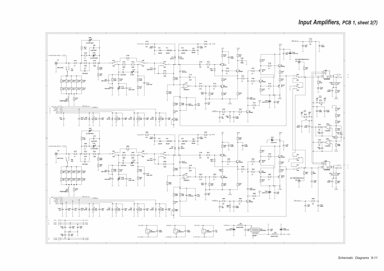
Input Amplifiers, PCB 1, sheet 2(7)
Schematic Diagrams 9-11
5
5
4
4
3
3
2
2
1
1
D D
C C
B B
A A
TRG_LVL_A
TRG_LVL_B
FILTER_A
FILTER_BTRG_LVL_B
TRG_LVL_A
FILTER_B
FILTER_A
TRG_LVL_A1
TRG_LVL_B1
+12VI
+5VAI+5VBI
-5.2VAI-5.2VBI
+5VAI-5.2VAI
-5.2VAI
+5VAI+12VI
+5VAI
-5.2VAI
+12VI
-5.2VBI
-5.2VBI
+5VBI+12VI +5VBI
-5.2VBI
+12VI
-5.2VAI
-5.2VAI
-5.2VBI
-5.2VAI
+5VBI+5VAI
-5.2VAI
+5VBI
+5VBI
-5.2VBI -5.2VAI
+5VAI
+5VAI5+5VBI5
-5.2VAI5-5.2VBI5
+12VI5
IMP A5ATT A5
AC/DC A5COM A5
FILTER_A5
IMP B5ATT B5
AC/DC B5COM B5
FILTER_B5
REAR PANEL INPUT A9
REAR PANEL INPUT B9
AN 6
B 6
BN 6
A 6
LE
LE
R24082R24082
L55
BLM21A102S
L55
BLM21A102S
R244
47
R244
47
1M
R191
1M
R191
R613
1K
R613
1K
10NC12510NC125
C9
1.5pF-500V
C9
1.5pF-500V
BAV99
D10
BAV99
D10
C143
3-10PF
C143
3-10PF
R184220R184220
R241
68
R241
68
R177120R177120
34
2K2A
UD2
K2A
UD2
C1622.2UF-6.3VC1622.2UF-6.3V
Q13BFR92AQ13BFR92A
R181150R181150
R248120R248120
R163120R163120
R188470KR188470K
R251150R251150
R167
47
R167
47
10NC503
10NC503
C151100NF
C151100NF
34
2K7A
UD2
K7A
UD2
BAV99
D17
BAV99
D17
R16047R16047
10NC23910NC239
R19947KR19947K
R169
68
R169
68
BAV99
D20
BAV99
D20
34
2K4A
UD2
K4A
UD2
10NC243
10NC243
3
26
-
+
U2A
LMC6081A
-
+
U2A
LMC6081A
C12222NF-200VC12222NF-200V
R215
680K
R215
680K
BFT93Q7BFT93Q7
R147330R147330
10N
C237
10N
C237
Q5BFR92AQ5BFR92A
R237120R237120
R212
47
R212
47
C132100NF
C132100NF
J10
BNC-COAX
J10
BNC-COAX
C144Not UsedC144Not Used
X34X34
Q16BFR92AQ16BFR92A
R1901KR1901K
BAV99
D31
BAV99
D31
R148680KR148680K
R24612KR24612K
C20
27PF
C20
27PF
18
+
-
K6CUD2
+
-
K6CUD2
R19510K
R19510K
C140
47P
C140
47P
R254470KR254470K
10NC22710NC227
Q10BFR93AQ10BFR93A
342
K1A
UD2
K1A
UD2
R216
220K
R216
220K
C2410PF-500V
C2410PF-500V
R2111KR2111K
Q14BFR92AQ14BFR92A
R610
1.2M
R610
1.2M
10NC15610NC156
R193
330
R193
330
R236120R236120
R253150R253150
C133100NFC133100NF
R247120R247120
R1801KR1801K
C117
3.9pF-100V
C117
3.9pF-100V
R182470KR182470K
R220680KR220680K
R213
470K
R213
470K
10NC15810NC158
V+
8
V-
4
U50CTLE2022CU50CTLE2022C
10NC24010NC240
R179150R179150
R2333.3R2333.3
10NC210NC2
10NC16310NC163
10NC246
10NC246
C7
1.5pF-500V
C7
1.5pF-500V
R229470KR229470K
X35X35
R17068R17068
C123
2.2UF-6.3V
C123
2.2UF-6.3V
C126100NF
C126100NF
18
+
-
K1CUD2
+
-
K1CUD2
R15547KR15547K
R194
27
R194
27
BAV99
D34
BAV99
D34
BAV99
D12
BAV99
D12
Q2BFR93AQ2BFR93A
R223
47
R223
47
V+
7
V-
4
U1BLMC6081AU1BLMC6081A
R18310KR18310K
C496
2.5-10PF/250V
C496
2.5-10PF/250V
R165120R165120
R145
100
R145
100
65
7K4B
UD2
K4B
UD2
10NC24410NC244
C139100NFC139100NF
R189470KR189470K
C165100NFC165100NF
R17412KR17412K
R18727R18727
10NC22910NC229
R132
100
R132
100
R176120R176120
R207
100
R207
100
100KR159100KR159
R138
0
R138
0
R149
10M
R149
10M
R1972K
R1972K
C260Not UsedC260Not Used
10NC12410NC124
J7A
NOT USED MINICOAX-3-5
J7A
NOT USED MINICOAX-3-5
R201
470
R201
470
18
+
-
K8CUD2
+
-
K8CUD2
R1581MR1581M
R135
10
R135
10
L54
BLM21A102S
L54
BLM21A102S
C146
27pF
C146
27pF
C159100NFC159100NF
C107100NFC107100NF
R250120R250120
10NC10010NC100 C101
100NFC101100NF
BAV99
D18
BAV99
D18R6111.2MR6111.2M
R2241K
R2241K
BAV99
D33
BAV99
D33
10N
C19
10N
C19
R196100KR196100K
R218
47
R218
47
R171
4.7K
R171
4.7K
R234120R234120
X36X36
1M
R262
1M
R262R260470KR260470K
R222
47
R222
47
C213.9PF-500V
C213.9PF-500V
C129100NFC129100NF
R214
120K
R214
120K
BAT18
D15
BAT18
D15
3
26
-
+
U1A
LMC6081A
-
+
U1A
LMC6081A
R202100R202100
10NC504
10NC504
C131
3.9pF-500V
C131
3.9pF-500V
R249120R249120
BAT18
D14
BAT18
D14
R261470KR261470K
R146
47
R146
47
10NC310NC3
BAV99
D30
BAV99
D30
R1533.3R1533.3
C103100NFC103100NF
10N
C235
10N
C235
C152220pC152220p
C160100NFC160100NF
C11839pFC11839pF
R235120R235120
C115
3.9pF-100V
C115
3.9pF-100V
10NC16410NC164
R24268R24268
R258
120K
R258
120K
R1920R1920
C166100NFC166100NF
R142
120K
R142
120K
R1851KR1851K
R239
47
R239
47
C120220pC120220p
R16882R16882
18
+
-
K5CUD2
+
-
K5CUD2
10NC10510NC105
18
+
-
K2CUD2
+
-
K2CUD2
R157
47
R157
47
BAT18
D21
BAT18
D21
R141
470K
R141
470K
BFT93Q15BFT93Q15
BFT92Q4BFT92Q4
R268100KR268100K
X37X37
R243
4.7K
R243
4.7K
R156470KR156470K
C116
3-10PF
C116
3-10PF
10NC24110NC241
Q3BFR92AQ3BFR92A
C149
3.9pF-100V
C149
3.9pF-100V
R210
100
R210
100
C102100NF
C102100NF
LE5
LE7
+10
-9
OUT2
OUT3
U3A
ADCMP565
U3A
ADCMP565
R1391KR1391K
6
57
+
-
U50B
TLE2022C
+
-
U50B
TLE2022C
C134
2.2UF-6.3V
C134
2.2UF-6.3V
R19815KR19815K
10NC24710NC247
10NC23010NC230
R2311MR2311M
BAV99
D11
BAV99
D11
Q1BF513Q1BF513
C15039pFC15039pF
BAV99
D36
BAV99
D36
C22
27PF
C22
27PF
C127100NF
C127100NF
BAT18
D22
BAT18
D22
R200
470
R200
470
100K
R154
100K
R154
C99
3.9pF-500V
C99
3.9pF-500V
R2031.5KR2031.5K
C234Not UsedC234Not Used
BAV99
D32
BAV99
D32
R133
470
R133
470
R136100R136100
BFT92Q12BFT92Q12
R208100R208100
C233.9PF-500V
C233.9PF-500V
R238150R238150
10NC24510NC245
10N
C231
10N
C231
C130100NFC130100NF
65
7K6B
UD2
K6B
UD2
342
K5A
UD2
K5A
UD2
BAV99
D37
BAV99
D37
10NC24210NC242
R2521KR2521K
R256220R256220
10NC23610NC236
Q6BFR92AQ6BFR92A
R166150R166150
R2253.3R2253.3
C110
22NF-200V
C110
22NF-200V
18
+
-
K4CUD2
+
-
K4CUD2
Q9BF513Q9BF513
BAV99
D19
BAV99
D19
V+
7
V-
4
U2BLMC6081AU2BLMC6081A
PCB-Pattern
L16NH
PCB-Pattern
L16NH
C6
1.5PF-500V
C6
1.5PF-500V
C108
100NF
C108
100NF
C148
3-10PF
C148
3-10PF
C111
3-10PF
C111
3-10PF
R143
680K
R143
680K
10N
C232
10N
C232
PCB-Pattern
L26NH
PCB-Pattern
L26NH
R137100R137100
LE17
LE15
+12
-13
OUT20
OUT19
U3B
ADCMP565
U3B
ADCMP565
R273
120K
R273
120K
R217
100
R217
100
10N
C238
10N
C238
R209
0
R209
0
C155
2.2UF-6.3V
C155
2.2UF-6.3V
34
2
K8A
UD2
K8A
UD2
R612
1K
R612
1K
C497
2.5-10PF/250V
C497
2.5-10PF/250V
C128100NFC128100NF
R134
470
R134
470
R22747
R22747
R2571KR2571K
R25510KR25510K
18
+
-
K7CUD2
+
-
K7CUD2
2
31
+
-
U50A
TLE2022C
+
-
U50A
TLE2022C
R25927R25927
10NC13610NC136
R144
220K
R144
220KR151
47
R151
47
C15422NF-200VC15422NF-200V
BAV99
D35
BAV99
D35
10NC15710NC157
R206
10
R206
10
R265
100
R265
100
R172
47
R172
47
R26710KR26710K
C141
22NF-200V
C141
22NF-200V
C138100NFC138100NF
R219330R219330
100KR232100KR232
Q8BFR92AQ8BFR92A
R230
47
R230
47
R245
47
R245
47
R175120R175120
R150
47
R150
47
R162120R162120
18
+
-
K3CUD2
+
-
K3CUD2
R164120R164120
C1612.2UF-6.3V
C1612.2UF-6.3V
C112Not UsedC112Not Used
R22847KR22847K
R264
27
R264
27
R1613.3R1613.3
C106
2.5-10PF/250V
C106
2.5-10PF/250V
R205180KR205180K
R140
47
R140
47
R2660R2660
C114
27pF
C114
27pF
Q11BFR92AQ11BFR92A
C147
3.9pF-100V
C147
3.9pF-100V
GN
D4
VC
C1
4
VE
E8
GN
D18
GN
D6
GN
D16
U3CADCMP565U3CADCMP565
J8
BNC-COAX
J8
BNC-COAX
J9A
NOT USED MINICOAX-3-5
J9A
NOT USED MINICOAX-3-5
BAV99
D13
BAV99
D13
C109
47P
C109
47P
R221
10M
R221
10M
C2510PF-500V
C2510PF-500V
65
7K2B
UD2
K2B
UD2
R263
330
R263
330
100K
R226
100K
R226
R173
47
R173
47
65
7
K8B
UD2
K8B
UD2
C119100NF
C119100NF
R178120R178120
34
2K6A
UD2
K6A
UD2
34
2K3A
UD2
K3A
UD2
C8
1.5PF-500V
C8
1.5PF-500V
10NC22810NC228
C1042.2UF-6.3VC1042.2UF-6.3V
C137
2.5-10PF/250V
C137
2.5-10PF/250V

9-12 Schematic Diagrams
This page is intentionally left blank.
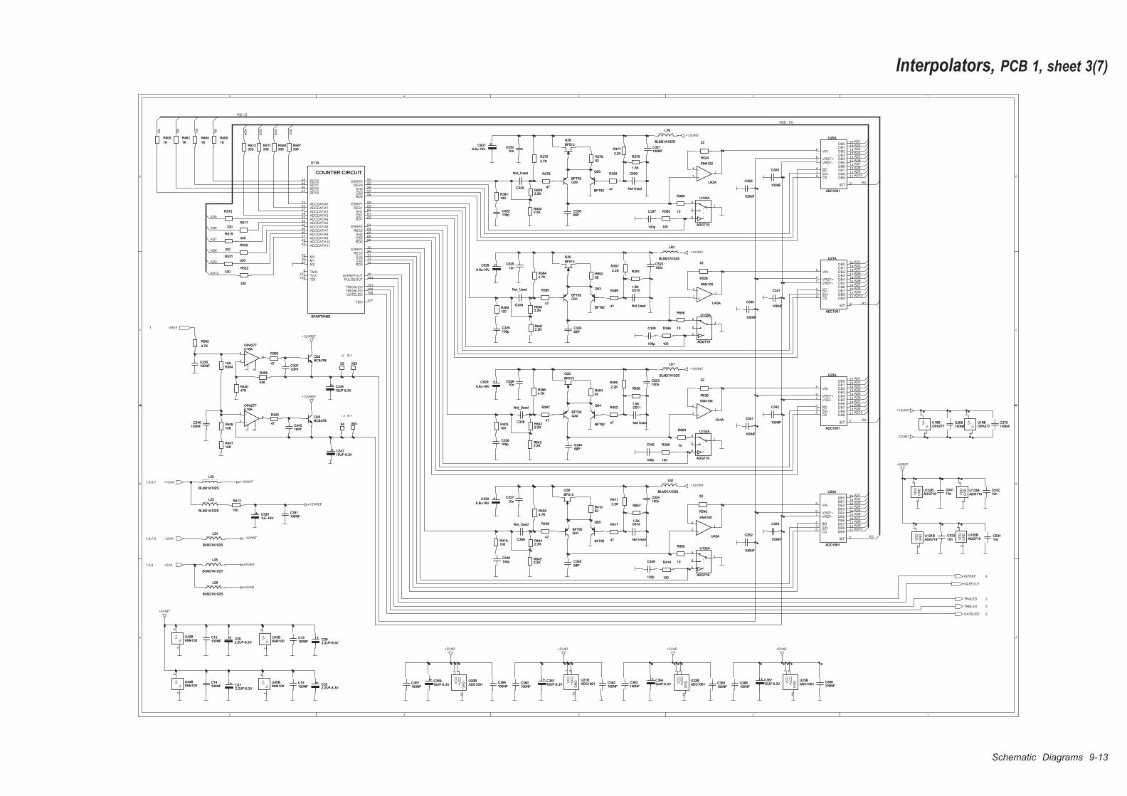
Interpolators, PCB 1, sheet 3(7)
Schematic Diagrams 9-13
5
5
4
4
3
3
2
2
1
1
D D
C C
B B
A A
AD9
AD7
AD2
AD10
AD2
AD2
AD8
AD4
AD6
AD5
AD9
AD1
AD5
AD1
AD8
AD3
AD6
AD10
AD8AD7
R3
AD9
AD7
AD10
AD5
AD7
R1
AD4
R0
AD6
AD4
AD5
AD6
AD8
AD8
AD6
AD2
AD10
AD3
AD3
R2
AD1
AD3
AD7
AD9
AD1
AD10
AD4AD5
AD9
R[0..3]
R0
R1
R2
R3
AD[1..10]
AD
1
AD
2
AD
3
AD
4
VREF1
GATEOUT
+12VINT
+12VREF
-12VINT
+5VINT
+5VAD
+12VINT
+12VINT
+12VINT
+12VINT
+12VREF
+12VREF
+5VAD+5VAD+5VAD+5VAD
-12VINT
+12VINT
+5VINT
+5VINT
+12VA1,5,6,7
-12VA1,6,7,8
+5VA1,5,6
TRALED 2
TRBLED 2
GATELED 2
INTREF 8
Hi REF
L o REF
C346
100p
C346
100p
R521
330
R521
330
R658
10
R658
10
R399
2.2K
R399
2.2K
R6432.2KR6432.2K
Q36
BF513
Q36
BF513
R380
10
R380
10C32668PC32668P
R540
22
R540
22
C334
Not_Used
C334
Not_Used
C323
100NF
C323
100NF
R6302.2KR6302.2K
C292.2UF-6.3VC292.2UF-6.3V
V+
5
V-
2
U44BKM4100U44BKM4100
R6452.2KR6452.2K
R416100R416100
R385
47
R385
47
R660
10
R660
10
C352
100NF
C352
100NF
L62
BLM21A102S
L62
BLM21A102S
V+
5
V-
2
U42BKM4100U42BKM4100
VD
D4
GN
D3
U135BADG719U135BADG719
10nC53110nC531
C338100pC338100p
C522100nC522100n
R520
330
R520
330
C33915UF-6.3VC33915UF-6.3V
C36715UF-6.3VC36715UF-6.3V
C3501uF-16VC3501uF-16V
R398
100
R398
100
8
21
6
U134A
ADG719
U134A
ADG719
R409
47
R409
47
BFT92Q29BFT92Q29
C530
6.8u-16V
C530
6.8u-16V
C342
100NF
C342
100NF
C324
100NF
C324
100NF
R391
1.5K
R391
1.5K
VC
C1
+V
CC
6
GN
D10
U21BADC1061U21BADC1061
C523100nC523100n
C509
Not Used
C509
Not UsedC325
Not_Used
C325
Not_Used
C368100NFC368100NF
R377
2.2K
R377
2.2K
C5076.8u-16V
C5076.8u-16V
BFT92
Q59
BFT92
Q59
8
21
6
U132A
ADG719
U132A
ADG719
X54X54
BFT92Q31BFT92Q31
C510
Not Used
C510
Not Used
INT2
S/H3
RD4
CS5
VREF-7
VIN8
VREF+9
DB218
DB119
DB020
DB614
DB515
DB416
DB317
DB713
DB812
DB911
U23A
ADC1061
U23A
ADC1061
C524100nC524100n
R383
47
R383
47
R379
1.5K
R379
1.5K
L23
BLM21A102S
L23
BLM21A102S
L22
BLM21A102S
L22
BLM21A102S
3
41
-
+
U45A
KM4100
-
+
U45A
KM4100
8
21
6
U135A
ADG719
U135A
ADG719
R519
330
R519
330
R528
22
R528
22
C351100NFC351100NF
C35568PC35568P
R3964.7KR3964.7K
C322.2UF-6.3VC322.2UF-6.3V
INT2
S/H3
RD4
CS5
VREF-7
VIN8
VREF+9
DB218
DB119
DB020
DB614
DB515
DB416
DB317
DB713
DB812
DB911
U22A
ADC1061
U22A
ADC1061C34510PFC34510PF
C349
100p
C349
100p
C529
6.8u-16V
C529
6.8u-16V
C353
100NF
C353
100NF
VC
C1
+V
CC
6
GN
D10
U23BADC1061U23BADC1061
BFT92Q34BFT92Q34
C36415UF-6.3VC36415UF-6.3V
INT2
S/H3
RD4
CS5
VREF-7
VIN8
VREF+9
DB218
DB119
DB020
DB614
DB515
DB416
DB317
DB713
DB812
DB911
U21A
ADC1061
U21A
ADC1061
INT2
S/H3
RD4
CS5
VREF-7
VIN8
VREF+9
DB218
DB119
DB020
DB614
DB515
DB416
DB317
DB713
DB812
DB911
U20A
ADC1061
U20A
ADC1061
R517
330
R517
330
R381100R381100
L25
BLM21A102S
L25
BLM21A102S
R375
4.7K
R375
4.7K
C33368PC33368P
VD
D4
GN
D3
U132BADG719U132BADG719
BFT92
Q65
BFT92
Q65
10nC53210nC532
V+
5
V-
2
U45BKM4100U45BKM4100
C14100NFC14100NF
R505
1K
R505
1K
Q33
BF513
Q33
BF513
X3X3 X53X53
C512
Not Used
C512
Not Used
L59
BLM21A102S
L59
BLM21A102S
R413
100
R413
100
R382
100
R382
100
R6402.2KR6402.2K
R397
47
R397
47
R39415KR39415K
R411
2.2K
R411
2.2K
R515
330
R515
330
R656
1.5K
R656
1.5K
C302.2UF-6.3VC302.2UF-6.3V
ERRP055
SH056
CS057
RD058
SH160
CS161
RD162
ERRP263
SH264
CS268
RD269
ERRP370
SH371
RES082
ERRP159
RES183
RES284
CS373
RD374
RES386
RDY044
RDY145
RDY246
RDY347
ADCDATA023
ADCDATA124
ADCDATA227
ADCDATA329
ADCDATA433
ADCDATA534
ADCDATA635
ADCDATA736
ADCDATA840
ADCDATA941
ADCDATA1042
ADCDATA1143
INTREFOUT10
PULSEOUT194
TRIGALED191
TRIGBLED192
GATELED198
M052
M150
M254
TMS2
TCK207
TDI159
TDO157
COUNTER CIRCUIT
U11A
SPARTANIIE
COUNTER CIRCUIT
U11A
SPARTANIIE
C341
100NF
C341
100NF
C528
6.8u-16V
C528
6.8u-16V
R6422.2KR6422.2K
R41082R41082
R403100R403100
R6292.2KR6292.2K
10n
C527
10n
C527
C12100NFC12100NF
R393
47
R393
47
10nC332
10nC332
BFT92
Q63
BFT92
Q63
C328100pC328100p
C363100NFC363100NF
VC
C1
+V
CC
6
GN
D10
U22BADC1061U22BADC1061
R6442.2KR6442.2K
R481
1K
R481
1K
3
41
-
+
U44A
KM4100
-
+
U44A
KM4100
L26
BLM21A102S
L26
BLM21A102S
R40482R40482
C322100pC322100p
V+
7
V-
4
U18BOPA277U18BOPA277
C335100NFC335100NF
C359100NFC359100NF
BFT92
Q64
BFT92
Q64
R507330R507330
VD
D4
GN
D3
U133BADG719U133BADG719
10nC53310nC533
R40710KR40710K
L24
BLM21A102S
L24
BLM21A102S
8
21
6
U133A
ADG719
U133A
ADG719
R40610KR40610K
V+
5
V-
2
U43BKM4100U43BKM4100
C321100NFC321100NF
R392
4.7K
R392
4.7K
10nC526
10nC526
3
26
1 8
-
+
U19AOPA277
-
+
U19AOPA277
R40047KR40047K
C36115UF-6.3VC36115UF-6.3V
R402
47
R402
47
Q28
BF513
Q28
BF513
Q30
BF513
Q30
BF513
R539
22
R539
22
L60
BLM21A102S
L60
BLM21A102S
C34468PC34468P
V+
7
V-
4
U19BOPA277U19BOPA277
R484
1K
R484
1K
C362100NFC362100NF
R659
10
R659
10
C329
100p
C329
100p
R65282R65282
VC
C1
+V
CC
6
GN
D10
U20BADC1061U20BADC1061
C348100pC348100p
R386
100
R386
100
R387
2.2K
R387
2.2K
R508330R508330
R3844.7KR3844.7K
C370100NFC370100NF
C331
100NF
C331
100NF
R485
1K
R485
1K
3
41
-
+
U42A
KM4100
-
+
U42A
KM4100
C15100NFC15100NF
R657
1.5K
R657
1.5K
X4X4C340100NF
C340100NF
3
26
1 8
-
+
U18AOPA277
-
+
U18AOPA277
C35815UF-6.3VC35815UF-6.3V
R511330R511330
R4084.7KR4084.7K
C360100NFC360100NF
C356
Not_Used
C356
Not_Used
R524
22
R524
22
C33710PFC33710PF
C511
Not Used
C511
Not Used
R395
33K
R395
33K
R37682R37682
10n
C525
10n
C525
VD
D4
GN
D3
U134BADG719U134BADG719
C34715UF-6.3VC34715UF-6.3V
10nC53410nC534
R405
47
R405
47
BFT92Q37BFT92Q37
C357100NFC357100NF
R522
330
R522
330
R389
47
R389
47
C312.2UF-6.3VC312.2UF-6.3V
C366100NFC366100NF
L61
BLM21A102S
L61
BLM21A102S
C369100NFC369100NF
Q32BC847BQ32BC847B
R414
100
R414
100
C330
100NF
C330
100NF
R390100R390100
Q35BC847BQ35BC847B
R513330R513330
3
41
-
+
U43A
KM4100
-
+
U43A
KM4100
C336
Not_Used
C336
Not_Used
R417
47
R417
47
C327
100p
C327
100p
R378
47
R378
47
C365100NFC365100NF
R6412.2KR6412.2K
C13100NFC13100NF

9-14 Schematic Diagrams
This page is intentionally left blank.
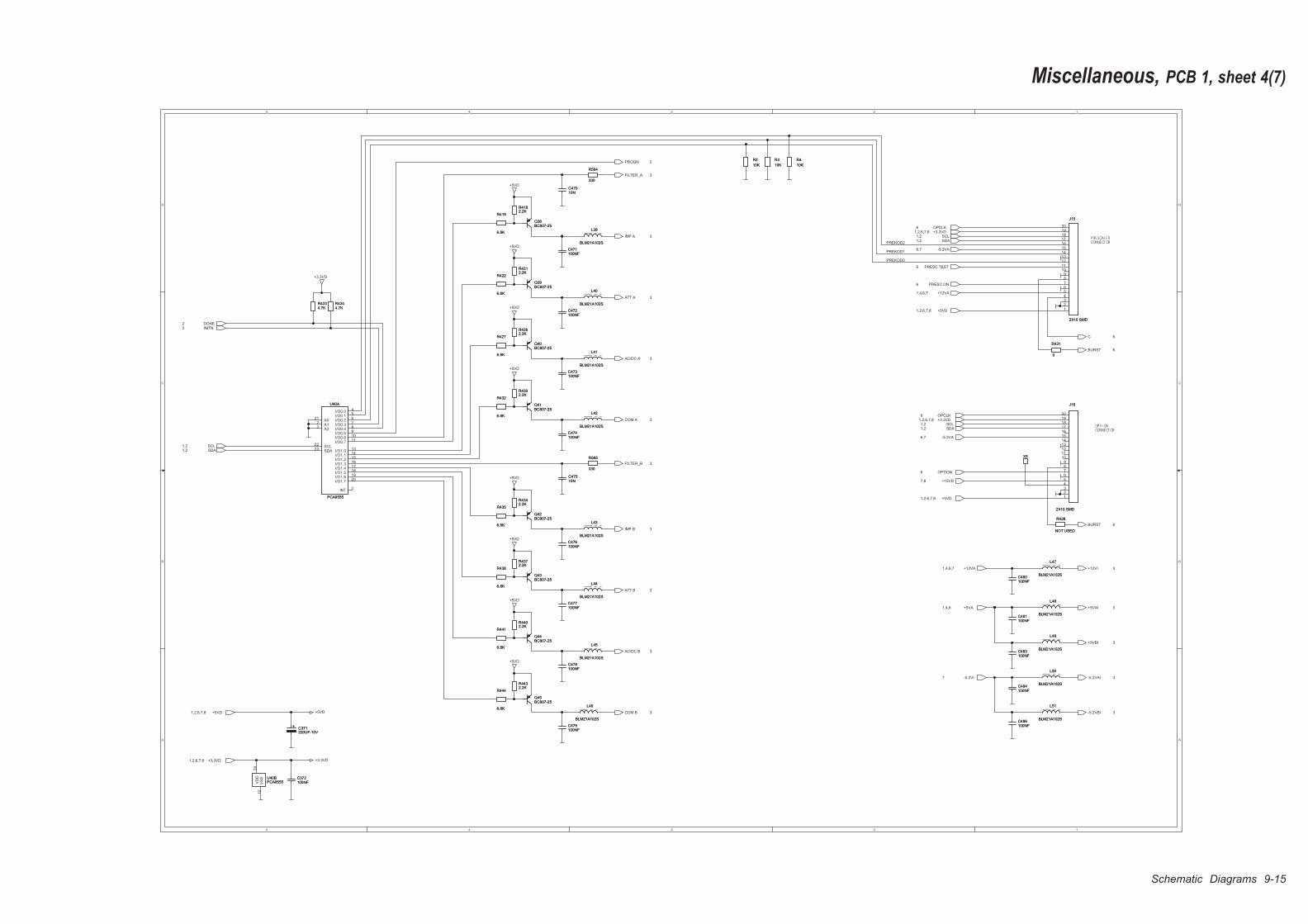
Miscellaneous, PCB 1, sheet 4(7)
Schematic Diagrams 9-15
5
5
4
4
3
3
2
2
1
1
D D
C C
B B
A A
PREKOD0
PREKOD2
PREKOD1
+5VD
+3.3VD
+5VD
+5VD
+5VD
+5VD
+5VD
+5VD
+5VD
+5VD
+3.3VD
SDA1,2SCL1,2
DONE2INITN2
+5VD1,2,6,7,8
+3.3VD1,2,6,7,8
OPCLK6+3.3VD1,2,6,7,8
SCL1,2SDA1,2
PRESC ON6
+5VD1,2,6,7,8
+12VA1,4,6,7
PRESC TEST6
+5VD1,2,6,7,8
OPTION6
OPCLK6+3.3VD1,2,6,7,8
SCL1,2SDA1,2
+12VA1,4,6,7
+5VA1,4,6
-5.2VI7
+15VD7,8
PROGN 2
IMP A 3
ATT A 3
AC/DC A 3
COM A 3
FILTER_B 3
BURST 6
C 6
BURST 6
FILTER_A 3
+12VI 3
+5VAI 3
+5VBI 3
-5.2VAI 3
-5.2VBI 3
AC/DC B 3
IMP B 3
ATT B 3
COM B 3
-5.2VA6,7
-5.2VA6,7
PRES CAL ERCONNECT OR
OPT I ONCONNECT OR
L39
BLM21A102S
L39
BLM21A102S
123456789
1011121314151617181920
J16
2X10 SMD
J16
2X10 SMD
R441
6.8K
R441
6.8K
C372100NFC372100NF
L47
BLM21A102S
L47
BLM21A102S
C478100NFC478100NF
R431
0
R431
0
C483100NFC483100NF
C473100NFC473100NF
R4372.2KR4372.2K
R4234.7KR4234.7K
R444
6.8K
R444
6.8K
L42
BLM21A102S
L42
BLM21A102S
C484100NFC484100NF
C471100NFC471100NF
R4
10K
R4
10K
123456789
1011121314151617181920
J15
2X10 SMD
J15
2X10 SMD
L48
BLM21A102S
L48
BLM21A102S
R4302.2KR4302.2K
R564
330
R564
330
C486100NFC486100NF
R4342.2KR4342.2K
R435
6.8K
R435
6.8K
Q41BC807-25Q41BC807-25
Q42BC807-25Q42BC807-25
VD
D24
VS
S12
U40BPCA9555U40BPCA9555
L46
BLM21A102S
L46
BLM21A102S
R428
NOT USED
R428
NOT USED
L51
BLM21A102S
L51
BLM21A102S
R565
330
R565
330
L50
BLM21A102S
L50
BLM21A102S
A021
A12
A23
SCL22
SDA23
I/O0.04
I/O0.15
I/O0.26
I/O0.37
I/O0.48
I/O0.59
I/O0.610
I/O0.711
I/O1.013
I/O1.114
I/O1.215
I/O1.316
I/O1.417
I/O1.518
I/O1.619
I/O1.720
INT1
U40A
PCA9555
U40A
PCA9555
10NC47010NC470
L45
BLM21A102S
L45
BLM21A102S
R427
6.8K
R427
6.8K
Q45BC807-25Q45BC807-25
Q43BC807-25Q43BC807-25
Q38BC807-25Q38BC807-25
C479100NFC479100NF
R4402.2KR4402.2K
X5X5
R4212.2KR4212.2K
C472100NFC472100NF
Q39BC807-25Q39BC807-25
R4182.2KR4182.2K
C476100NFC476100NF
R419
6.8K
R419
6.8K
R438
6.8K
R438
6.8K
10NC47510NC475
Q44BC807-25Q44BC807-25
Q40BC807-25Q40BC807-25
L43
BLM21A102S
L43
BLM21A102S
C371220UF-10VC371220UF-10V
C481100NFC481100NF
R3
10K
R3
10K
R4432.2KR4432.2K
R432
6.8K
R432
6.8K
L41
BLM21A102S
L41
BLM21A102S
L40
BLM21A102S
L40
BLM21A102S
R4262.2KR4262.2K
R4244.7KR4244.7K
C480100NFC480100NF
L44
BLM21A102S
L44
BLM21A102S
R422
6.8K
R422
6.8K
R2
10K
R2
10K
C474100NFC474100NF
L49
BLM21A102S
L49
BLM21A102S
C477100NFC477100NF

9-16 Schematic Diagrams
This page is intentionally left blank.
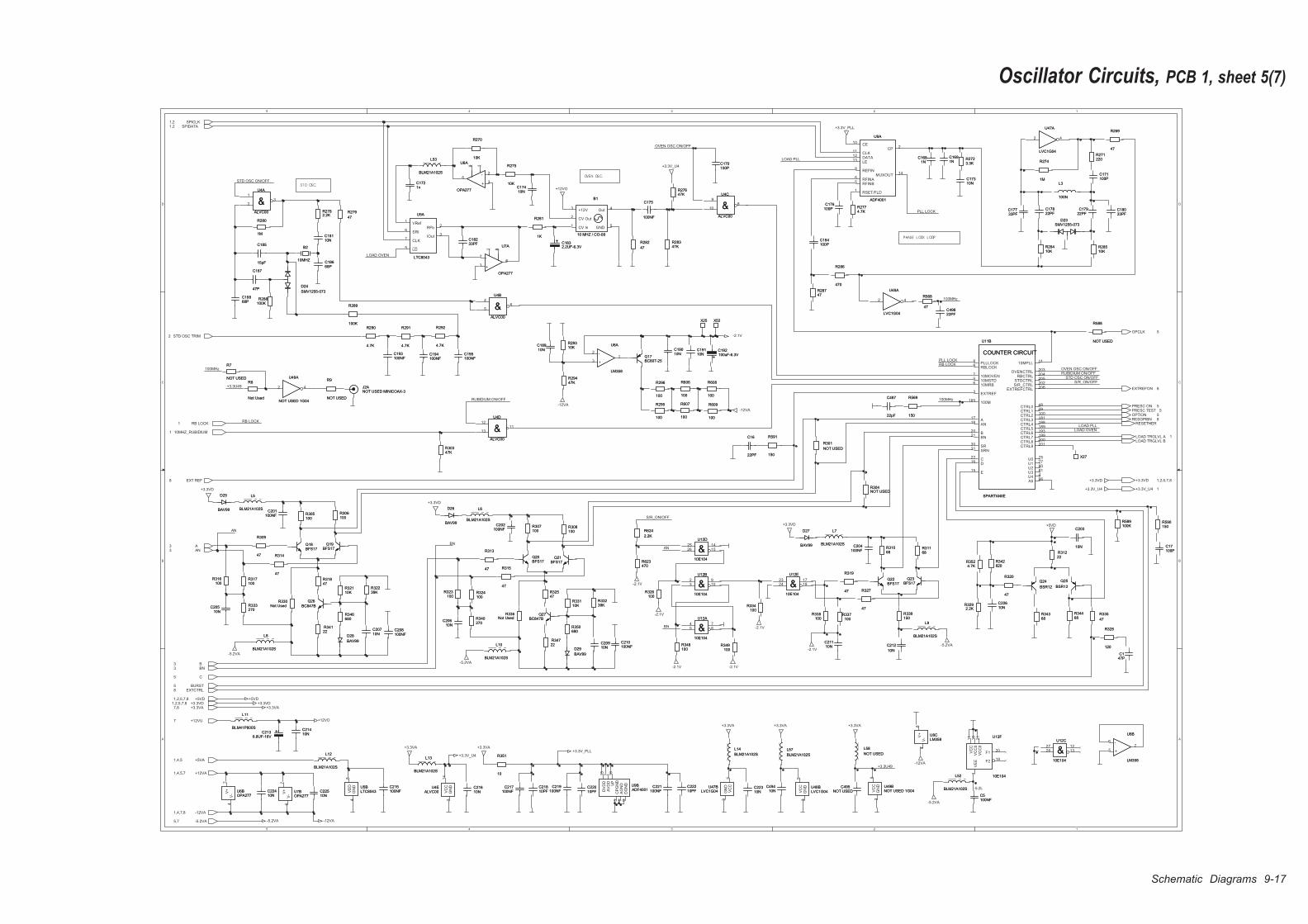
Oscillator Circuits, PCB 1, sheet 5(7)
Schematic Diagrams 9-17
5
5
4
4
3
3
2
2
1
1
D D
C C
B B
A A
STD OSC ON/OFF
OVEN OSC ON/OFF
RUBIDIUM ON/OFF
PLL LOCK
LOAD PLL
PLL LOCKRB LOCK
AN
AN
BN
LOAD OVEN
LOAD OVENLOAD PLL
OVEN OSC ON/OFFRUBIDIUM ON/OFF
STD OSC ON/OFF
100MHz
100MHz
-5.2L
RB LOCK
100MHz
+3.3U49
+3.3U49
S/R_ON/OFF
S/R_ON/OFF
BN
10MHZ_RUBIDIUM1
RB LOCK1 RESETHER
LOAD TRGLVL A 1LOAD TRGLVL B
+3.3VD 1,2,5,7,8
+3.3V_U4 1
+12VO
-2.1V
+3.3V_PLL+3.3V_U4
+3.3V_U4
+12VO
+3.3V_PLL
+3.3VD
-5.2VA
+3.3VD
-5.2VA
-2.1V
-2.1V -2.1V
-2.1V
+5VD+3.3VD
-5.2VA
+3.3VA +3.3VA
+3.3VA
-5.2VA
-12VA
-12VA
-12VA
-2.1V
+3.3VD
+3.3V_U4
+3.3VA +3.3VA
-2.1V
-12VA-5.2VA
+3.3VA
+5VD+3.3VD
STD OSC TRIM2
EXT REF8
SPICLK1,2SPIDATA1,2
AN3A3
PRESC ON 5PRESC TEST 5OPTION 5RESGPIBN 8
EXTREFON 8
OPCLK 5
C5
+12VU7
B3
+12VA1,4,5,7
+5VA1,4,5
-12VA1,4,7,8
-5.2VA5,7
+3.3VA7,8+3.3VD1,2,5,7,8
BURST5
BN3
+5VD1,2,5,7,8
EXTCTRL8
S T D OSC.
OVEN OSC.
PHAS E L OCK L OOP
R28347KR28347K
BAV99
D25
BAV99
D25
L13
BLM21A102S
L13
BLM21A102S
R306100R306100
R275
10K
R275
10K
BAV99
D26
BAV99
D26
100K
R289
100K
R289
100KR589100KR589
Q23BFS17
Q23BFS17
10NC205
10NC205
R607
100
R607
100
R339150R339150
10NC17310NC173
R31068R31068
2
31
+
-
U8A
LM358
+
-
U8A
LM358
10NC21110NC211
R309
47
R309
47
R328
120
R328
120
2 4
U47A
LVC1G04
U47A
LVC1G04
R301
NOT USED
R301
NOT USED
R323100
R323100
R31222R31222
C204100NF
C204100NF
R591
150
R591
150
R624
2.2K
R624
2.2K
R271220R271220
VC
C5
GN
D3
U49BNOT USED 1G04U49BNOT USED 1G04
R326100
R326100
10NC21410NC214
L8
BLM21A102S
L8
BLM21A102S
X25X25
R316100
R316100
L6
BLM21A102S
L6
BLM21A102S
C193100NFC193100NF
C17822PFC17822PF
R292
4.7K
R292
4.7K
R307100R307100
R34468R34468
X52X52
C201100NF
C201100NF
R342820R342820
Q20BFS17Q20BFS17
10NC17410NC174
R350680R350680
C170100PC170100P
L58
NOT USED
L58
NOT USEDR351
10
R351
10
10NC494
10NC494
R320
47
R320
47
BAV99
D29
BAV99
D29
6
57
+
-
U8B
LM358
+
-
U8B
LM358
C210100NFC210100NF
R9
NOT USED
R9
NOT USED
R606
100
R606
100
L5
BLM21A102S
L5
BLM21A102S
R33239KR33239K
R2782.2KR2782.2K
C221100NF
C221100NF
C219100NF
C219100NF
R8
Not Used
R8
Not Used
2 4
U49A
NOT USED 1G04
U49A
NOT USED 1G04
CP2
RSET/FLD1
RFINB5
RFINA6
REFIN8
CLK11
DATA12
LE13
MUXOUT14
CE10
U9A
ADF4001
U9A
ADF4001
R3292.2K
R3292.2K
R32547R32547
R315
47
R315
47
1M
R274
1M
R274
R569
150
R569
150
BAV99
D28
BAV99
D28
10NC19010NC190
10NC22410NC224
R623470R623470
L7
BLM21A102S
L7
BLM21A102S
R317100R317100
R590150R590150
PLLLOCK8
RBLOCK9
10MOVEN7
10MSTD5
10MRB6
EXTREF3
100M185
10MPLL11
OVENCTRL203
RBCTRL204
STDCTRL205
S/R_CTRL202
EXTREFCTRL206
A17
AN18
B20
BN21
SR30
SRN31
C22
D16
E15
CTRL048
CTRL149
CTRL2100
CTRL3181
CTRL4188
CTRL5189
CTRL6193
CTRL7199
CTRL8200
CTRL9201
U075
U177
U280
U381
U44
A596
COUNTER CIRCUIT
U11B
SPARTANIIE
COUNTER CIRCUIT
U11B
SPARTANIIE
R335
47
R335
47
C487
22pF
C487
22pF
L57
BLM21A102S
L57
BLM21A102S
C192100uF-6.3VC192100uF-6.3V
R34122R34122
L52
BLM21A102S
L52
BLM21A102S
R336Not Used
R336Not Used
C5100NFC5100NF
1112
13 &ALVC00
U4D
&ALVC00
U4D
C215100NFC215100NF
Q17BC807-25Q17BC807-25
C17922PFC179
22PF
L11
BLM41P800S
L11
BLM41P800S
CV In1
CV Out2
+12V3
Out4
GND5
B1
10 MHZ / CO-08
B1
10 MHZ / CO-08
V+
7
V-
4
U6BOPA277U6BOPA277
R34722R34722
R282
47
R282
47
VC
C5
GN
D3
U47BLVC1G04
U47BLVC1G04
R2723.3KR2723.3K
C2136.8UF-16V
C2136.8UF-16V
10NC22610NC226
R338100
R338100
10NC22510NC225
L10
BLM21A102S
L10
BLM21A102S
R290
4.7K
R290
4.7K
C1721nC1721n
R608
100
R608
100
C1691NC1691N
C187
47P
C187
47P
R31168R31168
R333270R333270
10NC206
10NC206
Q24
BSR12
Q24
BSR12
R348100R348100
R291
4.7K
R291
4.7K
R30347KR30347K
L12
BLM21A102S
L12
BLM21A102S
C18668PC18668P
10NC18110NC181
10N
C203
10N
C203
C22210PFC22210PF
2324 18
17
&U12E
10E104
&U12E
10E104
C1681N
C1681N
R269
47
R269
47
R340270R340270
Q19BFS17
Q19BFS17
L9
BLM21A102S
L9
BLM21A102S
R588
NOT USED
R588
NOT USED
Q25
BSR12
Q25
BSR12
Q22BFS17Q22BFS17
10NC20710NC207
C176100PC176
100P
C195100NFC195100NF
R29310KR29310K
R32239KR32239K
VRef1
RFb2
SRI6
CLK7
LD5
IOut3
U5A
LTC8043
U5A
LTC8043
R270
10K
R270
10K
R28747R28747
R31847R31847
C217100NF
C217100NFV
DD
8
GN
D4
U5BLTC8043U5BLTC8043
2728 13
12
&U12C
10E104
&U12C
10E104
L53
BLM21A102S
L53
BLM21A102S
VE
E1
VC
C0
16
F219
VC
C1
1
F120
VC
C0
21 U12F
10E104
U12F
10E104
C16
22PF
C16
22PF
R33110KR33110K
23 10
9
&U12B
10E104
&U12B
10E104
2526 15
14
&U12D
10E104
&U12D
10E104
89
10 &ALVC00
U4C
&ALVC00
U4C
X27X27
45 8
7
&U12A
10E104
&U12A
10E104
C1832.2UF-6.3VC1832.2UF-6.3V
BAV99
D27
BAV99
D27
C171100PC171100P
L14
BLM21A102S
L14
BLM21A102S
R32110KR32110K
C18033PFC18033PF
VC
C5
GN
D3
U48BLVC1G04U48BLVC1G04
100KR288
100KR288
D23SMV1255-073
D23SMV1255-073
1M
R280
1M
R280
R313
47
R313
47
3
26
18
-
+
U6A
OPA277
-
+
U6A
OPA277
R28410KR28410K
Q27BC847B
Q27BC847B
D24
SMV1255-073
D24
SMV1255-073
R295
100
R295
100
V+
7
V-
4
U7BOPA277U7BOPA277
R304NOT USEDR304NOT USED
C18233PFC18233PF
10NC18910NC189
C495NOT USED
C495NOT USED
R281
1K
R281
1K
2 4
U48A
LVC1G04
U48A
LVC1G04
C18868PC18868P
L3
100N
L3
100N
C49822PFC49822PF
B2
10MHZ
B2
10MHZ
C185
15pF
C185
15pF
GN
D7
VC
C14
U4EALVC00
U4EALVC00
Q21BFS17
Q21BFS17
C175
100NF
C175
100NF
R334100
R334100
R568
47
R568
47
C21810PFC21810PF
10NC19110NC191
R324100R324100
R286
470
R286
470
R330Not Used
R330Not Used
10NC21610NC216
10NC22310NC223
R346680R346680
C17100PC17100P
R34368R34368
R29447KR29447K
R7
NOT USED
R7
NOT USEDR296
100
R296
100
R305100R305100
R327
47
R327
47
C194100NFC194100NF
Q18BFS17Q18BFS17
R2774.7KR2774.7K
R349100
R349100
R308100R308100
R27647KR27647K
C17733PFC17733PF
C202100NF
C202100NF
C147PC1
47P
R28510KR28510K
31
2 &ALVC00
U4A
&ALVC00
U4A
3
26
1 8
-
+
U7A
OPA277
-
+
U7A
OPA277
10N
C212
10N
C212
C208100NFC208100NF
10NC20910NC209
R3524.7K
R3524.7K
R337100
R337100
Q26
BC847B
Q26
BC847B
64
5 &ALVC00
U4B
&ALVC00
U4B
R609
100
R609
100
CP
GN
D3
AG
ND
4
AV
DD
7
DG
ND
9
DV
DD
15
VP
16
U9BADF4001U9BADF4001
R279
47
R279
47
C184100PC184100P
R319
47
R319
47
V+
8
V-
4
U8CLM358U8CLM358
J2ANOT USED MINICOAX-3J2ANOT USED MINICOAX-3
R314
47
R314
47
C22010PFC22010PF

9-18 Schematic Diagrams
This page is intentionally left blank.
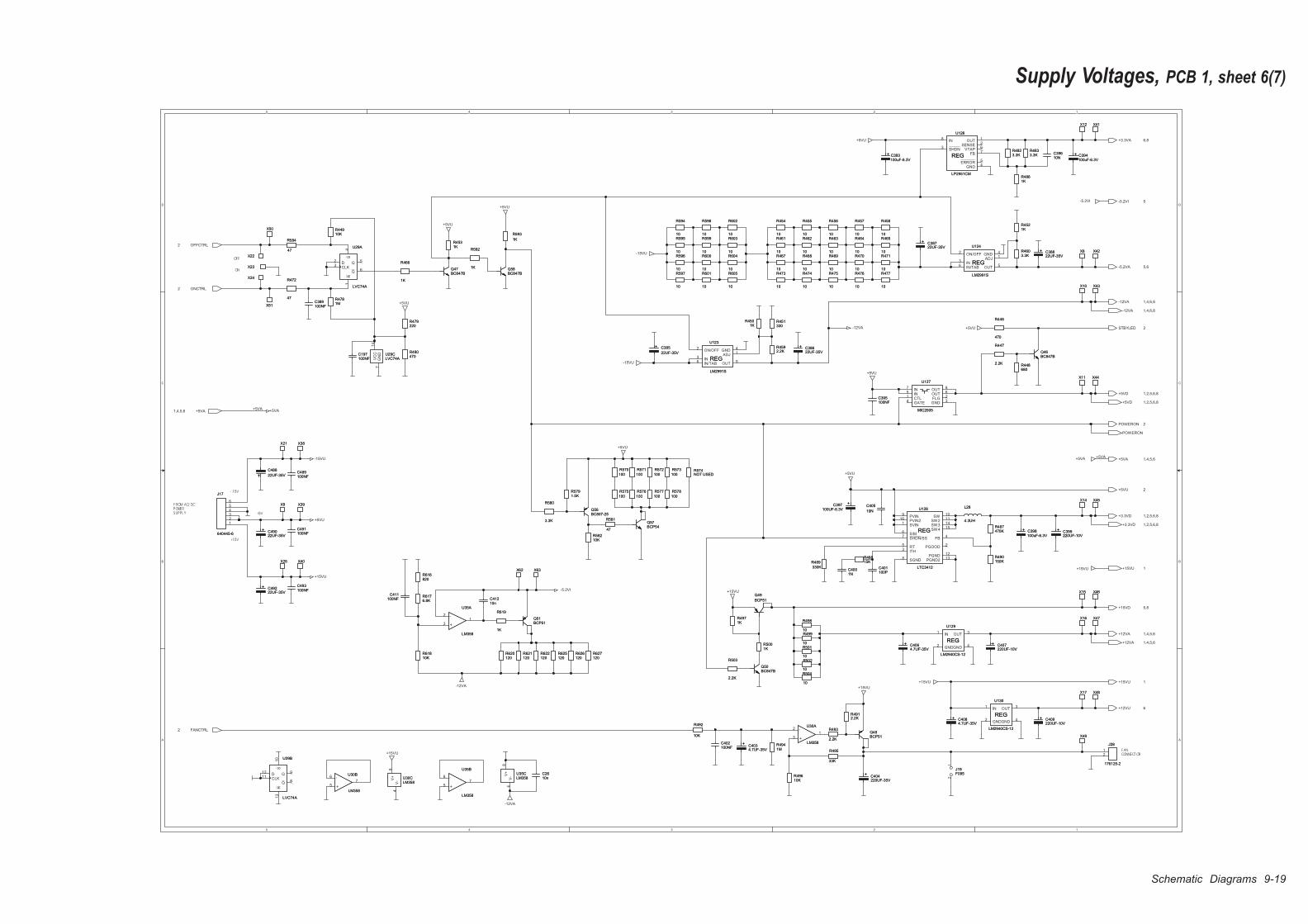
Supply Voltages, PCB 1, sheet 6(7)
Schematic Diagrams 9-19
5
5
4
4
3
3
2
2
1
1
D D
C C
B B
A A
+5VA
+5VA
+15VU 1
POWERON
+5VD 1,2,5,6,8
+3.3VD 1,2,5,6,8
+12VA 1,4,5,6
-12VA 1,4,6,8
+5VA1,4,5,6
+5VU
-15VU
+15VU
-12VA
-5.2VI
+5VA
+5VU
+5VU
+5VU
+5VU
+5VU
+5VU
+5VU
-15VU
-15VU
+15VU
+15VU
+15VU
+5VU
+15VU
+15VU-12VA
-5.2VI
+5VA
-12VA
OFFCTRL2
ONCTRL2
FANCTRL2
-5.2VA 5,6
-12VA 1,4,6,8
+5VD 1,2,5,6,8
+3.3VA 6,8
+3.3VD 1,2,5,6,8
+5VU 2
POWERON 2
+15VU 1
+15VD 5,8
+12VA 1,4,5,6
+12VU 6
STBYLED 2
+5VA 1,4,5,6
-5.2VI 5
FROM AC/ DCPOWERS UPPL Y
- 15V
+5V
+15V
FANCONNECT OR
ON
OFF
R503
2.2K
R503
2.2K
R601
10
R601
10
C389100NFC389100NF
R474
10
R474
10
R616820R616820
R4823.3KR4823.3K
R599
10
R599
10
R476
10
R476
10
6
57
+
-U30B
LM358+
-U30B
LM358
R4592.2KR4592.2K
R4501K
R4501K
R448680R448680
C4064.7UF-35VC4064.7UF-35V
R5001KR5001K
L28
4.3UH
L28
4.3UH
C393100uF-6.3VC393100uF-6.3V
X63X63
R574NOT USEDR574NOT USED
R471
10
R471
10
R6176.8KR6176.8K
R447
2.2K
R447
2.2K
C488
22UF-35V
C488
22UF-35V
X12X12
C395100NFC395100NF
10NC39610NC396
R470
10
R470
10
R596
10
R596
10
R595
10
R595
10
R577
100
R577
100
R580
3.3K
R580
3.3K
R626120R626120
R49610KR49610K
X39X39
R581
47
R581
47
V+
8
V-
4
U30CLM358U30CLM358
X44X44
IN3
OUT5
ADJ1
GND4
ON/OFF2
IN/TAB6
REG
U123
LM2991S
REG
U123
LM2991S
X11X11
R570
100
R570
100
Q51BCP51Q51BCP51
X26X26
R458
10
R458
10R593
1K
R593
1K
R592
1K
R592
1K
R603
10
R603
10
R571
100
R571
100
R58210KR58210K
R44910KR44910K
R504
10
R504
10
R468
10
R468
10
IN1
OUT3
GND2
GND4
REG
U129
LM2940CS-12
REG
U129
LM2940CS-12
C38622UF-35VC38622UF-35V
C489100NFC489100NF
R597
10
R597
10
PVIN9
PVIN216
SVIN1
FB4
PGND12
PGND213
SGND8
S/M6
SHDN/SS7
PGOOD2
RT5
ITH3
SW10
SW211
SW314
SW415
REG
U128
LTC3412
REG
U128
LTC3412
IN8
OUT1
SHDN3
GND4
SENSE2
ERROR5
VTAP6
FB7
REG
U126
LP2951CM
REG
U126
LP2951CM
IN3
OUT5
ADJ1
GND4
ON/OFF2
IN/TAB6
REG
U124
LM2991S
REG
U124
LM2991S
R598
10
R598
10
V+
8
V-
4
U35CLM358U35CLM358
X51X51
Q57BCP54Q57BCP54
X10X10
C4001NC4001N
C398100uF-6.3VC398100uF-6.3V
C493100NFC493100NF
R451330R451330
Q58BC847BQ58BC847B
R456
10
R456
10
R622120R622120
X43X43
6
57
+
-
U35B
LM358
+
-
U35B
LM358
R461
10
R461
10
R473
10
R473
10
X22X22
D12
CLK11
S1
0R
13
Q9
Q8
U29B
LVC74A
U29B
LVC74A
CTL1
FLG2
GATE4
GND3
IN7
IN5
OUT8
OUT6
U127
MIC2505
U127
MIC2505
X38X38
R4861KR4861K
C402100NFC402100NF
Q46BC847BQ46BC847B
C409220UF-10VC409220UF-10V
R4833.3KR4833.3K
X48X48
R5791.5KR5791.5K
R602
10
R602
10
X50X50
C394100uF-6.3VC394100uF-6.3V
C401100PC401100P
X42X42
C4084.7UF-35VC4084.7UF-35V
Q49
BCP51
Q49
BCP51
X15X15
R620120R620120
R4521KR4521K
R4603.3KR4603.3KR467
10
R467
10
C38722UF-35VC38722UF-35V
R627120R627120
VC
C1
4
GN
D7
U29CLVC74AU29CLVC74A
12
J19F095J19F095
C38822UF-35VC38822UF-35V
R573
100
R573
100
R493
2.2K
R493
2.2K
X47X47
123456
J17
640445-6
J17
640445-6
R479220R479220
R487470KR487470K
R495
33K
R495
33K
X41X41
2
31
+
-
U35A
LM358
+
-
U35A
LM358
C49022UF-35VC49022UF-35V
R4971KR4971K
330K
R489
330K
R489
C397100UF-6.3V
C397100UF-6.3V
1MR4941MR494
R578
100
R578
100
C4034.7UF-35VC4034.7UF-35V
C197100NFC197100NF
R605
10
R605
10
R604
10
R604
10
R466
1K
R466
1K
10nC41210nC412
C385
22UF-35V
C385
22UF-35V
12
J28
176125-2
J28
176125-2
R600
10
R600
10
R625120R625120
R498
10
R498
10
X62X62
R502
10
R502
10
X24X24
Q50BC847BQ50BC847B
C404220UF-35VC404220UF-35V
R4912.2KR4912.2K
R465
10
R465
10
Q47BC847BQ47BC847B R475
10
R475
10
R454
10
R454
10
R472
47
R472
47
R499
10
R499
10
R576
100
R576
100
X23X23
10nC2610nC26
X46X46
X16X16
2
31
+
-U30A
LM358+
-U30A
LM358
C399220UF-10VC399220UF-10V
X17X17
R48815KR48815K
R469
10
R469
10
R4531KR4531K
X9X9
R492
10K
R492
10K
1MR4781MR478
X14X14
R584
47
R584
47
R457
10
R457
10R463
10
R463
10
D2
CLK3
S4
R1
Q5
Q6
U29A
LVC74A
U29A
LVC74A
Q56BC807-25Q56BC807-25
C491100NFC491100NF
R619
1K
R619
1K
R477
10
R477
10
R621120R621120
10N
C405
10N
C405
C407220UF-10VC407220UF-10V
R446
470
R446
470
R462
10
R462
10
IN1
OUT3
GND2
GND4
REG
U130
LM2940CS-12
REG
U130
LM2940CS-12
C411100NF
C411100NF
R455
10
R455
10
X8X8
R61810KR61810K
C49222UF-35VC49222UF-35V
X49X49
R501
10
R501
10
X21X21
X40X40
R572
100
R572
100
Q48BCP51Q48BCP51
X45X45
R490150KR490150K
R480470R480470
R575
100
R575
100
R464
10
R464
10
R594
10
R594
10

This page is intentionally left blank.
9-20 Schematic Diagrams
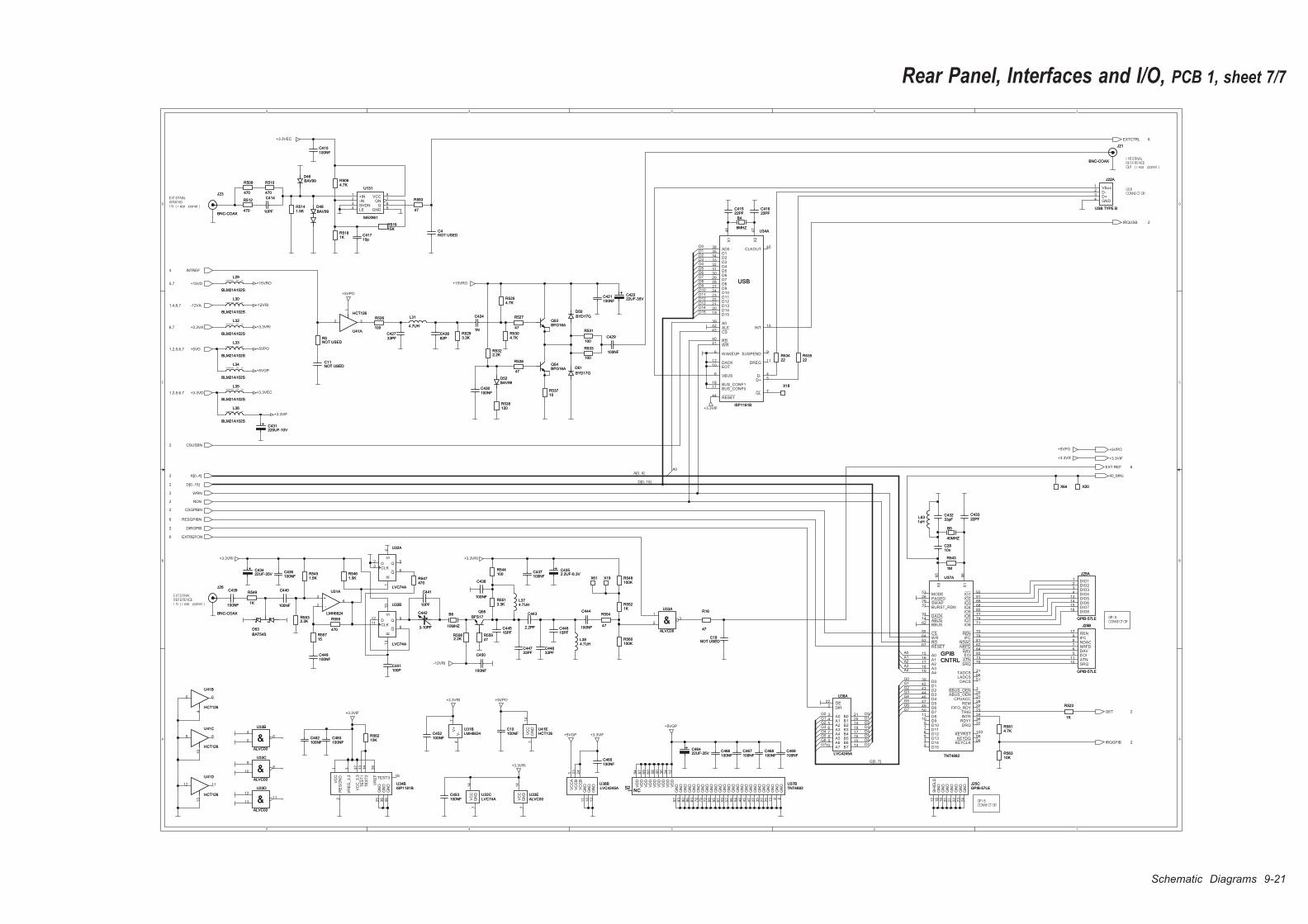
Rear Panel, Interfaces and I/O, PCB 1, sheet 7/7
Schematic Diagrams 9-21
5
5
4
4
3
3
2
2
1
1
D D
C C
B B
A A
G0G1G2
G6G7
G0G1G2
G5G6G7
G3
G5G4
G3G4
G[0..7]
D1
D0
D5
D6
D10
D8
D13
D3
D12
D[0..15]
D7
D2
D5
D7
D14
D11
D6
D4
D0
D1
D2
D15
D4
D9
D3
A[0..4]
A4
A0
A2
A0A1
A3
40_MHz
+3.3VIF
+5VPO
+15VRO
-12VRI
+3.3VRI
+3.3VEC
+3.3VIF
+5VPO
+5VGP
+3.3VEC
+3.3VIF
+15VRO
-12VRI
+3.3VRI +3.3VRI
+3.3VRI
+5VGP +3.3VIF
+5VGP
+3.3VIF
+3.3VRI
+5VPO
+5VPO
+3.3VIF
+5VPOCSUSBN2
RESGPIBN6
CSGPIBN2
RDN2
WRN2
DIRGPIB2
D[0..15]2
INTREF4
A[0..4]2
EXTREFON6
+15VD5,7
-12VA1,4,6,7
+3.3VA6,7
+3.3VD1,2,5,6,7
+5VD1,2,5,6,7
GET 2
IRQGPIB 2
IRQUSB 2
EXTCTRL 6
EXT REF 6
I NT ERNALREFERENCEOUT ( r ear panel )
EXT ERNALARMI NGI N ( r ear panel )
USBCONNECT OR
EXT ERNALREFERENCEI N ( r ear panel )
GPI BCONNECT OR
GPI BCONNECT OR
R531
100
R531
100
B4
6MHZ
B4
6MHZ
R549
1K
R549
1K
L384.7UHL384.7UH
R5513.3KR5513.3K
R547470R547470
C469100NFC469100NF
C41622PFC41622PF
C44833PFC44833PF
VC
C14
GN
D7
U41EHCT126U41EHCT126
+IN1
-IN2
SHDN3
LE4
VCC8
QN7
Q6
GND5
U131
MAX961
U131
MAX961
R555
470
R555
470
C11NOT USEDC11NOT USED
10nC2810nC28
R5322.2KR5322.2K
C429
100NF
C429
100NF
C410100NFC410100NF
R53710R53710
C43422UF-35VC43422UF-35V
C18NOT USED
C18NOT USED
C452100NFC452100NF
R5064.7KR5064.7K
C41522PFC41522PF
BAV99D46BAV99D46
OE22
DIR2
A03
A14
A25
A36
A47
A58
A69
A710
B021
B120
B219
B318
B417
B516
B615
B714
U38A
LVC4245A
U38A
LVC4245A
AD038
D135
D234
D333
D432
D531
D630
D729
D828
D927
D1024
D1123
D1222
D1321
D1420
D1519
A039
ALE42
CS43
RD40
WR41
INT15
SUSPEND9
WAKEUP8
DREG11
DACK12
EOT10
BUS_CONF118
BUS_CONF017
GL7
X1
48
X2
47
VBUS6
D-4
D+5
RESET44
CLKOUT45
USB
U34A
ISP1181B
USB
U34A
ISP1181B
10MHZ
B6
10MHZ
B6
VC
C1
VC
C_
3,3
37
TE
ST
113
TE
ST
214
TEST316
GN
D2
5
GN
D3
6
GN
D4
6
RE
GG
ND
2
VR
EG
_3,3
3
VR
EF
26
U34BISP1181BU34BISP1181B
C466100NFC466100NF
X64X64
VC
C14
GN
D7
U32CLVC74AU32CLVC74A
R5254.7KR5254.7K
R583
47
R583
47
C4NOT USEDC4NOT USED
C467100NFC467100NF
R509
470
R509
470
C4352.2UF-6.3VC4352.2UF-6.3V
D12
CLK11
S1
0R
13
Q9
Q8
U32B
LVC74A
U32B
LVC74A
BAT54S
D53
BAT54S
D53
VC
CA
1
VC
CB
23
VC
CB
24
GN
D1
1
GN
D1
2
GN
D1
3
U38BLVC4245AU38BLVC4245A
C44515PFC44515PF
C43322PFC43322PF
R53522R53522
R5582.2KR5582.2K
X18X18
REN17
IFC9
NDAC8
NRFD7
DAV6
EOI5
ATN11
SRQ10
J25B
GPIB-57LE
J25B
GPIB-57LE
C450
100NF
C450
100NF
DRQ32
RDY138
X0
95
X1
96
A015
A116
A217
A318
A419
D039
D142
D243
D344
D446
D547
D649
D750
D811
D910
D109
D117
D126
D135
D143
D152
CS55
WR64
RD63
RESET67
INTR34
TRIG23
IO192
IO291
IO389
IO488
IO580
IO677
IO774
IO871
SRQ76
ATN73
EOI85
DAV84
NRFD82
NDAC81
IFC79
REN70
ABUS14
BBUS62
DACK33
BURST_RDN31
FIFO_RDY30
SWAP29
REM28
ABUS_OEN20
BBUS_OEN1
PAGED26
CPUACC22
MODE53
TADCS21
LADCS66
DACS51
KEYRST100
KEYCLK98
KEYDQ99
GPIBCNTRL
U37A
TNT4882
GPIBCNTRL
U37A
TNT4882
Q55
BFS17
Q55
BFS17
1112
13 &ALVC00
U33D
&ALVC00
U33D
R56210KR56210K
C42222UF-35VC42222UF-35V
1M
R543
1M
R543
D50
BYD17G
D50
BYD17G
DIO11
DIO22
DIO33
DIO44
DIO513
DIO614
DIO715
DIO816
J25A
GPIB-57LE
J25A
GPIB-57LE
L29
BLM21A102S
L29
BLM21A102S
R5521KR5521K
L36
BLM21A102S
L36
BLM21A102S
R5141.5KR5141.5K
L631uHL631uH
V+
7
V-
4
U31BLMH6624U31BLMH6624
VBus1
D-2
D+3
GND4
J22A
USB TYPE B
J22A
USB TYPE B
R538120R538120
C449100NFC449100NF
R5NOT USEDR5NOT USED
VD
D1
2V
DD
24
VD
D3
6V
DD
40
VD
D5
8
VD
D6
9
VD
D6
0
VD
D8
7V
DD
94
GN
D4
GN
D8
GN
D1
3
GN
D2
7
GN
D2
5
GN
D3
5G
ND
37
GN
D4
1G
ND
45
GN
D4
8G
ND
54
GN
D5
6G
ND
57
GN
D5
9G
ND
61
GN
D6
5G
ND
68
GN
D7
2G
ND
75
GN
D7
8G
ND
83
GN
D8
6G
ND
90
GN
D9
3G
ND
97
NC52
U37BTNT4882
NC52
U37BTNT4882
GN
D1
8
GN
D1
9
GN
D2
0
GN
D2
1
GN
D2
2
GN
D2
3
GN
D2
4
SH
IELD
12
J25CGPIB-57LEJ25CGPIB-57LE
R55715R55715
R53422R53422
C41710pC41710p
L30
BLM21A102S
L30
BLM21A102S
9 8
10
U41C
HCT126
U41C
HCT126
C440
100NF
C440
100NF
C44733PFC44733PF
31
2 &ALVC00
U33A
&ALVC00
U33A
C443
2.2PF
C443
2.2PF
5 6
4
U41B
HCT126
U41B
HCT126
R5532.2KR5532.2K
C44615PFC44615PF
C463100NFC463100NF
R512
470
R512
470
R51615KR51615K
D51
BYD17G
D51
BYD17G
C465100NFC465100NF
R56310KR56310K
C414
10PF
C414
10PF
C436100NFC436100NF
L31
4.7UH
L31
4.7UH
GN
D7
VC
C14
U33EALVC00U33EALVC00
L374.7UHL374.7UH
L34
BLM21A102S
L34
BLM21A102S
D2
CLK3
S4
R1
Q5
Q6
U32A
LVC74A
U32A
LVC74A
R523
1K
R523
1K
C441
10PF
C441
10PF
R5293.3KR5293.3K
R5461.5KR5461.5K
X20X20
X19X19
C468100NFC468100NF
J21
BNC-COAX
J21
BNC-COAX
X61X61
C462100NFC462100NF
R16
47
R16
47
R55947R55947
R5614.7KR5614.7K
2
36
+
-
U31A
LMH6624
+
-
U31A
LMH6624
64
5 &ALVC00
U33B
&ALVC00
U33B
Q54BFG16AQ54BFG16A
R526
100
R526
100
J26
BNC-COAX
J26
BNC-COAX
Q53BFG16AQ53BFG16A
R544100R544100
L32
BLM21A102S
L32
BLM21A102S
R536
47
R536
47
C437100NFC437100NF
C42882PC42882P
C430100NFC430100NF
BAV99
D48
BAV99
D48
C43233pFC43233pF
R533
100
R533
100
C424
1N
C424
1NR5304.7KR5304.7K
R5181KR5181K
C421100NFC421100NF
12 11
13
U41D
HCT126
U41D
HCT126
C46422UF-35VC46422UF-35V
2 3
1
U41A
HCT126
U41A
HCT126
100KR560100KR560
C451100PC451100P
R5451.5KR5451.5K
C42733PFC42733PF
C438
100NF
C438
100NF
89
10 &ALVC00
U33C
&ALVC00
U33C
R527
47
R527
47
J23
BNC-COAX
J23
BNC-COAX
L33
BLM21A102S
L33
BLM21A102S
100KR548100KR548
C439
100NF
C439
100NF
C442
3-10PF
C442
3-10PF
C453100NFC453100NF
R510
470
R510
470
C444
100NF
C444
100NF
C431220UF-10VC431220UF-10V
L35
BLM21A102S
L35
BLM21A102S
R554
47
R554
47
BAV99D52BAV99D52
C10100NFC10100NF
40MHZ
B5
40MHZ
B5
Display & Keyboard, PCB 2, Component Layout
9-22 Schematic Diagrams
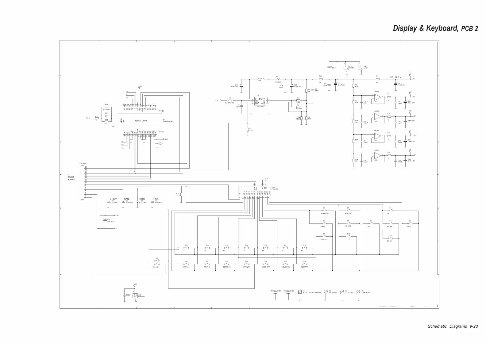
Display & Keyboard, PCB 2
Schematic Diagrams 9-23
5
5
4
4
3
3
2
2
1
1
D D
C C
B B
A A
V0
V0
V1
V4
V0
V2
V3
V3
V2
V1
V4
+3.3V
+5V
+3.3V
+3.3V
+3.3V
+3.3V
+5V
+3.3V
Title
Size Document Number Rev
Modify Date: Sheet o f
Project
01
Display and Keyboard Board
Pendulum Instruments AB
A2
1 1
4031 100 65860May 28, 2004
CNT-90/91
Web Site = www.pendulum.se
15.0 - 17.6 V
STDBY GATE TRIGATRIGB
TO
BASIC
BOARD
L1
10uH
S24
USER OPT
C11100nF
R18
10
H13.2 PLATED SQUARE PAD
S20
INPUT A
C7
100nF
C15100nF
S3
UP
C1622uF-6.3V
R1
47
U1CLM358
V+
8
V-
4
S18
F7
+
-
U2A
LM358
2
31
C533pF
S10
C
S14
F3
D3EL414GD
J1FPC 20
NC
1N
C2
NC
3N
C4
NC
5N
C6
FR
7LP
8D
OF
F9
EIO
10
VD
D11
VS
S12
V4
13
V1
14
V0
15
NC
16
NC
17
NC
18
NC
19
NC
20
S25
HOLD/RUN
L2
BLM21A102S
U3BPCA9555V
DD
24
VS
S12
S21
INPUT B
C9100nF
H23.5 PLATED
R5
10
R13
10
C13100nF
S8
RIGHT
C222.2uF-35V
S19
StandBy
C8100nF
C1100nF
U2CLM358
V+
8
V-
4
S1
MEAS FUNC
R334.7K
R174.7K
S6
LEFT
C202.2uF-35V
S15
F4
D4EL414GD
TP3
R20
47
C1822uF-6.3V
PROBE GND1
U3A
PCA9555
A0
21
A1
2A
23
SC
L22
SD
A23
I/O
0.0
4I/O
0.1
5I/O
0.2
6I/O
0.3
7I/O
0.4
8I/O
0.5
9I/O
0.6
10
I/O
0.7
11
I/O
1.0
13
I/O
1.1
14
I/O
1.2
15
I/O
1.3
16
I/O
1.4
17
I/O
1.5
18
I/O
1.6
19
I/O
1.7
20
INT
1
R35
Not used
S26
RESTART
1MR2
H33.5 PLATED
S22
SETTINGS
470K
R4
320x97 DOTSE1TM32097AGFG
+
-
U1B
LM358
6
57
C6100nF
R10
10
C2522uF-6.3V
820KR8
S13
F2
TP2
C19
100nF
C10100nF
PROBE GND2
S2
AUTO SET
C44.7uF-35V
R194.7K
S11
DOWN
REG
U4
TPS61045
L1
VIN2
CTRL5
GND6
SW8
DO3
FB4
PGND7
S16
F5
D5EL414GD
R14
10
H43.5 PLATED
R34.7K
S4
VALUE
R6
Not used
S23
MATH/LIM
+
-
U1A
LM358
2
31
C14100nF
C34.7uF-35V
R16
10
TP4J2FPC 20
NC
1
V0
2
V2
3
V3
4
VS
S5
MD
6
FR
7
LP
8
DO
FF
B9
XC
K10
DI7
11
DI6
12
DI5
13
DI4
14
DI3
15
DI2
16
DI1
17
DI0
18
VD
D19
NC
20
S12
F1
+
-
U2B
LM358
6
57
C12100nF
100KR9
S7
ENTER
C21
100nF
D2EL414ID
C17100nF
S9
STAT PLOT
S17
F6
R344.7K
TP5
S5
OK EXIT
R74.7K
C232.2uF-35V
C2422uF-6.3V
10BQ030
D1
J3
2x10 SMD
1234567891011121314151617181920
R11
10
R1533K
TP1

This page is intentionally left blank
9-24 Schematic Diagrams
Version B
The descriptions in this section apply to instru-
ments having a Sharp microprocessor.
See General Information on page III for details on
relevant serial numbers etc.
Schematic Diagrams 9-25

This page is intentionally left blank.
9-26 Schematic Diagrams
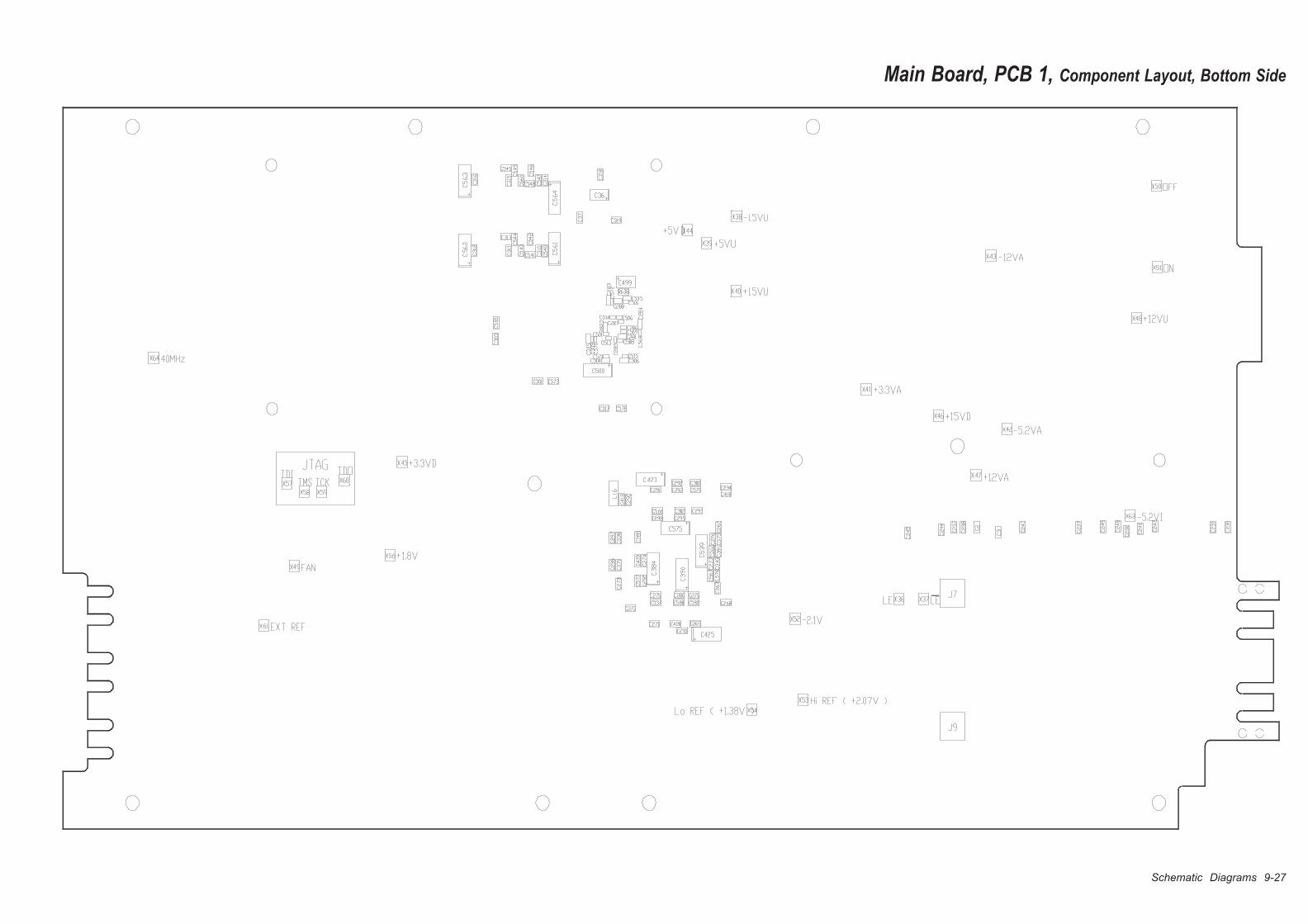
Main Board, PCB 1, Component Layout, Bottom Side
Schematic Diagrams 9-27
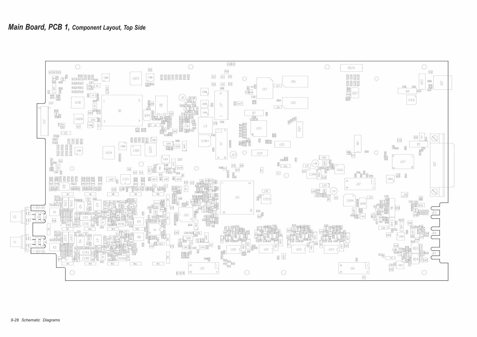
Main Board, PCB 1, Component Layout, Top Side
9-28 Schematic Diagrams
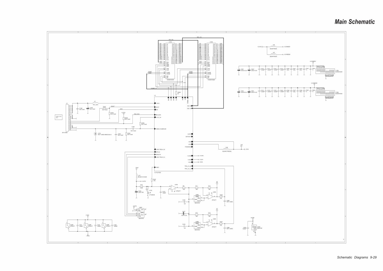
Main Schematic
Schematic Diagrams 9-29
5
5
4
4
3
3
2
2
1
1
D D
C C
B B
A A
DOUT
A0A1A2A3A4A5A6A7A8A9A10A11
A13A14
A0A1A2A3A3A4A5A6A7A8
A10A11
A13A14
D24D25D26D27D28D29D30D31
D IN
RB LOCK
D[0..31]
A[0..23]
D3D20
D0
D6
D15
D11
D18
D22
D4D19
D7
D9
D12
D23
D1
D13
D16
D5
D2
D8
D14
D17
D10
D21
A9
DQM2DQM3
DQM[0..3]
DQM0DQM1
A12 A12
+5VTR
+5VA
+3.3VD
+12VA
-12VA
+5VTR
+3.3VMEM2
+3.3VMEM1
+5VA
+12VA
-12VA
+5VTR
+3.3VD
+3.3VMEM1
+3.3VMEM2
+3.3VD
1
RUB I DI UMOS C.
U15BK4S561632D
VD
D1
VD
D14
VD
D27
VD
DQ
3
VD
DQ
9
VD
DQ
43
VD
DQ
49
VS
S2
8
VS
S4
1
VS
S5
4
VS
SQ
6
VS
SQ
12
VS
SQ
46
VS
SQ
52
R6
100
R14
10K
C561100uF-6.3V
L67
BLM41P800S
R66922
J27ANOT USED MINICOAX-3
C200Not Used
C196Not Used
C381100NF
-
+
U26A
OPA277
3
26
1 8
L27
BLM21A102S
C383100NF
C542100n
C482NOT USED
R302Not Used
-
+
U28A
OPA277
3
26
1 8
C310100NF
C5601n
R299Not Used
C546100n
R297
Not Used
C562100uF-6.3V
L4
Not_used
C382100NF
C485NOT USED
C374100NF
-
+
U24A
OPA277
3
26
1 8
C375
1nF
DAC
U46C
MAX5156
UPO11
DOut10
PDL12
CL5
CS6
DIn7
SClk8
C5431n
C315100NF
C547100n
C311100NF
U16A
K4S561632D
A023
A124
A225
A326
A429
A530
A631
A732
A833
A934
A1022
A1135
A1236
I/O02
I/O14
I/O25
I/O37
I/O48
I/O510
I/O611
I/O713
I/O842
I/O944
I/O1045
I/O1147
I/O1248
I/O1350
I/O1451
I/O1553
RAS18
WE16
CS19
CAS17
LDQM15
BA020
BA121
UDQM39
CKE37
CLK38
DACU46A
MAX5156
RefA4
FBA3
OutA2
U122
LT1009CD46
5
8
H1
3.5 PLATED
10MHZ_RUBIDIUM
RB LOCK
DIN
DOUT
+15VU
A[0..23]
D[0..31]
CS
WE
CLK
CK
E
LOAD TRGLVL A
LOAD TRGLVL B
SPICLK
SPIDATA
VREFTRG_LVL_A
TRG_LVL_B
GATEOUT
+5VPO
+3.3V_U4
+5VD
+5VA
POWERON
+3.3VD
+12VA
-12VA
CA
S
RA
S
DQ
M[0
..3
]
U26BOPA277
V+
7
V-
4
C314100NF
R11
10K
R566
100
C563100uF-6.3V
C377
15UF-6.3V
R4451.5K
C540100n
C378
1nF
R298Not Used
C5441n
U16BK4S561632DV
DD
1
VD
D1
4
VD
D2
7
VD
DQ
3
VD
DQ
9
VD
DQ
43
VD
DQ
49
VS
S2
8
VS
S4
1
VS
S5
4
VS
SQ
6
VS
SQ
12
VS
SQ
46
VS
SQ
52
J11
2X10 SMD
1234567891011121314151617181920
R300Not Used
C548100n
C313100NF
X6
C199
Not Used
R13
10K
X13
U15A
K4S561632D
A023
A124
A225
A326
A429
A530
A631
A732
A833
A934
A1022
A1135
A1236
I/O02
I/O14
I/O25
I/O37
I/O48
I/O510
I/O611
I/O713
I/O842
I/O944
I/O1045
I/O1147
I/O1248
I/O1350
I/O1451
I/O1553
RAS18
WE16
CS19
CAS17
LDQM15
BA020
BA121
UDQM39
CKE37
CLK38
X7
L66
BLM41P800S
C316100NF
DACU46B
MAX5156
RefB13
FBB14
OutB15 U46D
MAX5156VD
D1
6
DG
ND
9
AG
ND
1
L56
BLM41P800S
U28BOPA277
V+
7
V-
4
C564100uF-6.3V
R12
10K
C312100NF
C37622UF-35V
U24BOPA277
V+
7
V-
4
C380100NF
C541100n
C198Not Used
R567
100
R10
2.2K
C545100NF
C5491n

9-30 Schematic Diagrams
This page is intentionally left blank.
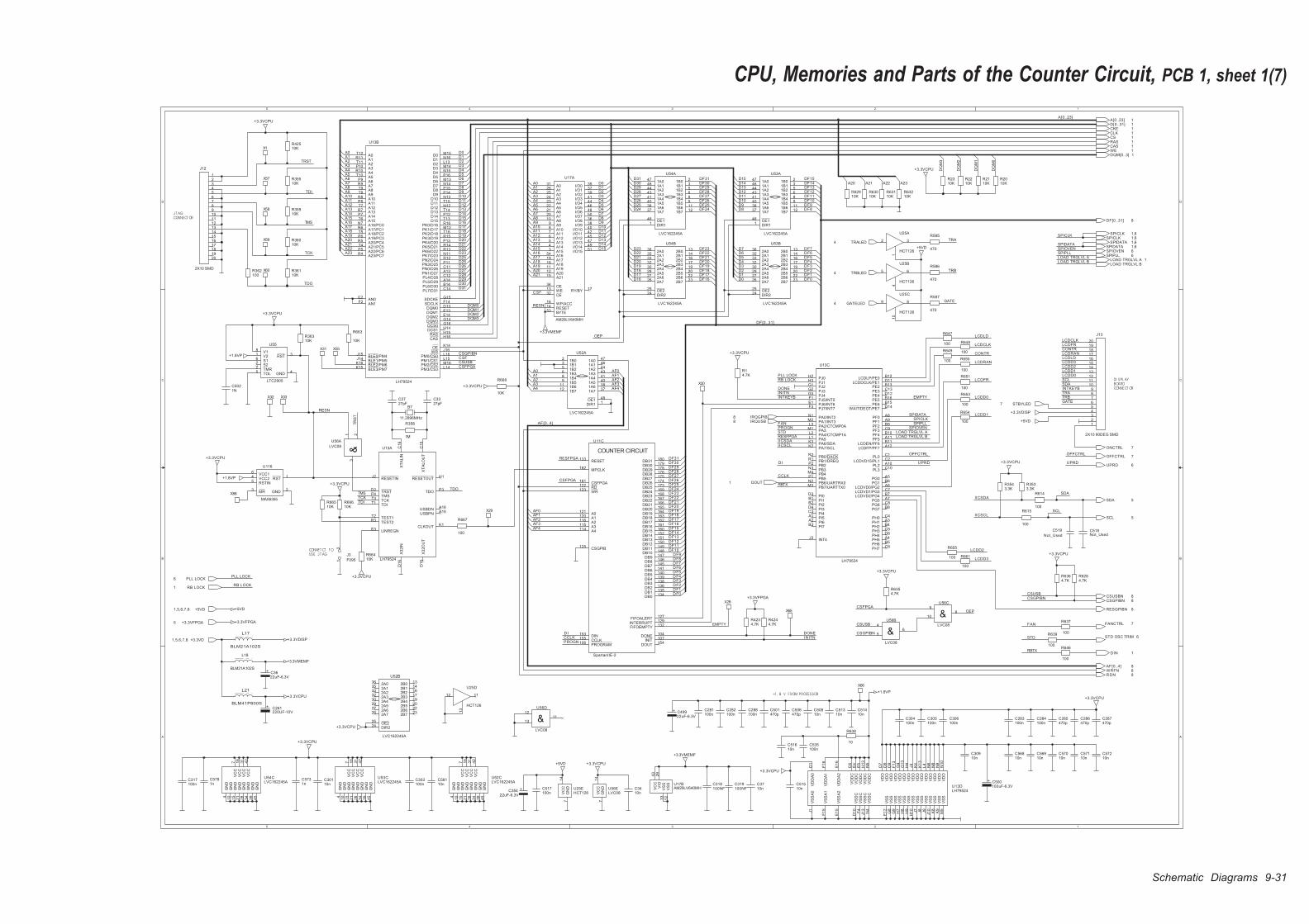
CPU, Memories and Parts of the Counter Circuit, PCB 1, sheet 1(7)
Schematic Diagrams 9-31
5
5
4
4
3
3
2
2
1
1
D D
C C
B B
A A
TCK
CSF
AF3AF4
DF16DF15DF14DF13DF12
DF9DF8DF7DF6DF5DF4DF3DF2DF1DF0
DF11DF10
SPICLKSPIDATA
SPIOVENSPIPLL
LOAD TRGLVL ALOAD TRGLVL B
EMPTY
TDI
TMS
TDO
TRST
SPICLK
SPIDATASPIOVENSPIPLLLOAD TRGLVL ALOAD TRGLVL B
DICCLKPROGN
DONE
PROGN
CCLK
INITN
D I
LCDCLK
LCDD3
GATETRBTRAINTKEYB
CSGPIBN
CSFPGA
DONEINITN
CSUSB
A[0..23]
DF24
DF17
DF27
DF21
DF31
DF25
DF28
DF22
DF19
DF29
DF23
DF26
DF20
DF30
DF18
DF31DF30DF29DF28DF27DF26DF25DF24
DF23DF22DF21DF20DF19DF18DF17DF16
DF15DF14DF13DF12DF11DF10DF9DF8
DF7DF6DF5DF4DF3DF2DF1DF0
DF[0..31]
DQ
M0
DQ
M3
DQ
M2
DQ
M1
CSGPIBN
CSUSB
OEP
OEP
D4
D12
D9
D2
D8
D0
D11
D7
D1
D13
D3
D6
D10
D5A16
A1
A19
A18
A9
A20
A3A2
A3A11
A21
A15
A16
A20
A2
A3
A5
A19
A7
A18
A21
A1
A11
A4
A13
A13
A1
A12
A7
A6
A14
A17
A17 A10
A8
A0
A6
A2
A9
A10A4
A0
A8
A5
A12
A15
A4
A0
A14
DQM0DQM1DQM2DQM3
TMSTCKTDI
TDO
RESN
TR
ST
CSGPIBNCSFCSUSBCSFPGA
AF1
AF4
AF1
AF3
AF2
AF[0..4]
AF0
AF0
AF2
A21 A22 A23A20
RESN
FAN
STDRESFPGA
RESFPGA
RBTX
OFFCTRL
EMPTY
IICSCL
IICSDAIICSCL
LCDFR
LCDD0
LCDD2
LCDRANCONTR
LCDLD
LCDD1
SCL
INTKEYB
CSFPGA
TRA
TRB
GATE
FAN
STD
RBTX
LCDCLK
LCDLD
CONTR
LCDRAN
LCDFR
LCDD0
LCDD1
LCDD2
LCDD3
A22A23
RB LOCKPLL LOCK
RB LOCK
PLL LOCK
D9
D0
D29
D4
D4
D24
D17
D31
D19
D21
D22
D7
D9
D7D6
D20
D18
D25
D11
D30
D29
D25
D8
D28
D14
D19
D23
D24
D30
D17
D16
D23
D13
D27
D12
D5
D26
D6D14
D15
D20
D27 D18
D16
D3
D2
D31
D10
D10
D14
D26D11
D28
D5
D21
D0
D13
D1
D8
D3
D2D1
D15D22
D12
D15
UPRD
SDA
SDA
SCL
IICSDA
OFFCTRL
UPRD
CAS 1RAS 1
DQM[0..3] 1
CS 1CLK 1CKE 1
WE 1
DIN 1
A[0..23] 1D[0..31] 1
SPIDATA 1,6
SPICLK 1,6
LOAD TRGLVL A 1LOAD TRGLVL B
DOUT1
RB LOCK1
+3.3VMEMF
+3.3VCPU
+3.3VDISP
+5VD
+3.3VCPU
+3.3VCPU
+3.3VCPU
+1.8VP
+5VD
+3.3VDISP
+3.3VCPU
+3.3VMEMF
+3.3VFPGA
+3.3VMEMF
+3.3VCPU
+3.3VCPU
+3.3VFPGA
+3.3VCPU
+3.3VCPU
+3.3VCPU
+3.3VCPU
+3.3VCPU
+3.3VCPU
+3.3VCPU
+5VD
+5VD
+3.3VCPU
+1.8VP
+3.3VCPU
+3.3VCPU
+1.8VP
+3.3VD1,5,6,7,8
TRALED4
TRBLED4
GATELED4
STBYLED7
+5VD1,5,6,7,8
SDA 5
SCL 5
SPICLK 1,6
OFFCTRL 7
SPIDATA 1,6
RDN 8
CSGPIBN 8CSUSBN 8
WRFN 8
ONCTRL 7
DF[0..31] 8
SPIOVEN 6SPIPLL 6
IRQUSB8IRQGPIB8
STD OSC TRIM 6
FANCTRL 7
AF[0..4] 8
+3.3VFPGA5
RESGPIBN 8
PLL LOCK6
UPRD 6
J T AGCONNECT OR
DI S P L AYBOARDCONNECT OR
CONNET CT T OUS E J T AG
+1. 8 V FROM PROCES SOR
R651
100
X60
C5781n U17B
AM29LV640MHVC
C43
VIO
29
VS
S52
VS
S33
U55
LTC2905
V18
V21
S16
S27
GND4
RST3
TMR2
TOL5
R35910K
R639
100
X55
10nC568
R2210K
U52CLVC162245A
GN
D4
GN
D10
GN
D15
GN
D21
GN
D28
GN
D34
GN
D39
GN
D45
VC
C7
VC
C3
1
VC
C4
2
VC
C1
8
X66
C518Not_Used
R14.7K
C317100n
J3
F09512
R63010K
R3543.3K
R646
100
10nC572
C303100n
100nC282
R4234.7K
U53B
LVC162245A
2A036
2A135
2A233
2A332
2A430
2A529
2A627
2A726
2B013
2B114
2B216
2B317
2B419
2B520
2B622
2B723
OE225
DIR224
R587
470
R36310K
470pC501
X29
X30
R6354.7K
U13A
LH79524
RESETINJ2
RESETOUTH1
TRSTD2
TMSP4
TCKT3
TDIT1
TEST1T2
TEST2R3
LINREGNE3
TDOP3
USBDNA16
USBPNA15
CLKOUTK1
XT
AL
INC
16
XT
AL
OU
TC
15
X3
2IN
D1
6
X3
2O
UT
D1
5
X68
470pC285
10nC301
100nC304
10nC516
X33
J13
2X10 90DEG SMD
123456789
1011121314151617181920
U25C
HCT126
9 8
10
U53A
LVC162245A
1A047
1A146
1A244
1A343
1A441
1A540
1A638
1A737
1B02
1B13
1B25
1B36
1B48
1B59
1B611
1B712
OE148
DIR11
C35422uF-6.3V
10nC309
C519
Not_Used
U116
MAX6355
GND2
MR3
VCC16
VCC24
RSTIN5
RST1
R647
100
R2110K
10nC571
X1
J12
2X10 SMD
1234567891011121314151617181920
100nC288
&LVC08
U56D
1112
13
R654
100
U54B
LVC162245A
2A036
2A135
2A233
2A332
2A430
2A529
2A627
2A726
2B013
2B114
2B216
2B317
2B419
2B520
2B622
2B723
OE225
DIR224
R63110K
100nC283
R667
100
R638
10
&
LVC08
U56A
31 2
U52A
LVC162245A
1A047
1A146
1A244
1A343
1A441
1A540
1A638
1A737
1B02
1B13
1B25
1B36
1B48
1B59
1B611
1B712
OE148
DIR11
470pC286
R4244.7K
100nC305
C49922uF-6.3V
1M
R358
R36110K
10nC515
U17A
AM29LV640MH
A031
A126
A225
A324
A423
A522
A621
A720
A810
A99
A108
A117
A126
A135
A144
A153
A1654
A1719
A1818
A1911
A2012
A2115
I/O035
I/O137
I/O239
I/O341
I/O444
I/O546
I/O648
I/O750
I/O836
I/O938
I/O1040
I/O1142
I/O1245
I/O1347
I/O1449
I/O1551
OE34
WE13
CE32
RESET14
WP/ACC16
BYTE53
RY/BY17
U25A
HCT126
2 3
1
R42510K
U54A
LVC162245A
1A047
1A146
1A244
1A343
1A441
1A540
1A638
1A737
1B02
1B13
1B25
1B36
1B48
1B59
1B611
1B712
OE148
DIR11
10nC508
COUNTER CIRCUIT
U11C
SpartanIIE-2
DB31180
DB30179
DB29178
DB28176
DB27175
DB26174
DB25173
DB24169
DB23168
DB22167
DB21166
DB20165
DB19164
DB18163
DB17162
DB16161
DB15160
DB14152
DB13151
DB12150
DB11149
DB10148
DB9147
DB8146
DB7145
DB6141
DB5140
DB4139
DB3138
DB2136
DB1135
DB0134
FIFOALERT127
INTERRUPT129
MPCLK182
RD122
WR123
A0121
A1120
A2116
A3115
A4114
RESET133
DIN153
CCLK155
PROGRAM106
DONE104
INIT107
DOUT154
FIFOEMPTY132
CSFPGA181
CSGPIB125
C3327pF
X32
U54CLVC162245A
GN
D4
GN
D10
GN
D15
GN
D21
GN
D28
GN
D34
GN
D39
GN
D45
VC
C7
VC
C3
1
VC
C4
2
VC
C1
8
R6364.7K
10nC570
R653
100
C3622uF-6.3V
X28
R2010K
100nC535
C318100NF
R66510K
R614
100
R655
100
U25D
HCT126
12 11
13
100nC284
C517100n
C5731n
R585
470
C319100NF
U52B
LVC162245A
2A036
2A135
2A233
2A332
2A430
2A529
2A627
2A726
2B013
2B114
2B216
2B317
2B419
2B520
2B622
2B723
OE225
DIR224
&LVC08
U56B
64
5
470pC287
LVC08U56E
GN
D7
VC
C1
4
100nC306
R63210K
R663
10K
X58
R66410K
R36010K
L18
BLM21A102S
R648
100
R66610K
U13DLH79524
VD
DN
10
VD
DN
9V
DD
N8
VD
DN
6V
DD
L4
VD
DK
13
VD
DK
4V
DD
J4
VD
DH
4V
DD
G1
3V
DD
G4
VD
DF
13
VD
DD
9V
DD
D8
VD
DD
7
VS
SM
5V
SS
K9
VS
SK
8V
SS
J1
0V
SS
J9
VS
SJ8
VS
SJ7
VS
SH
10
VS
SH
9V
SS
H8
VS
SH
7V
SS
G9
VS
SG
8V
SS
E1
2
VD
DC
N5
VD
DC
H1
3V
DD
CE
5V
DD
CE
4V
DD
CD
5
VS
SC
N4
VS
SC
J1
3V
SS
CF
4V
SS
CD
10
VD
DA
0D
1V
SS
A0
J1
VD
DA
1F
16
VS
SA
1F
15
VD
DA
2E
16
VS
SA
2E
15
10nC513
R650
100
R62910K
R668
10K
R3533.3K
C2727pF
R2310K
R637
100
R6284.7K
10nC569
C5021N
R362100
11.2896MHz
B7
R615
100
R661
100
U13C
LH79524
PJ0H2
PJ1H3
PJ2G1
PJ3G2
PJ4G3
PJ5/INT5F1
PJ6/INT6E1
PJ7/INT7F3
PA0/INT2N1
PA1/INT3M2
PA2/CTCMP0AL3
PA3M1
PA4/CTCMP1AL2
PA5L1
PA6/SDAK3
PA7/SCLK2
PB0/DACKR2
PB1/DREQR1
PB2P2
PB3N3
PB4M4
PB5P1
PB6/UARTRX0N2
PB7/UARTTX0M3
PI0D3
PI1B1
PI2B2
PI3D4
PI4C3
PI5A1
PI6A2
PI7B3
INT4J3
LCDLP/PE0B12
LCDDCLK/PE1D11
PE2B13
PE3C13
PE4D12
PE5B16
PE6B15
WAIT/DEOT/PE7D14
PF0A8
PF1A9
PF2B9
PF3C9
PF4B10
PF5A11
LCDEN/PF6B11
LCDFP/PF7A12
PL0C1
LCDVD15/PL1C2
PL2A10
PL3C10
PG0A5
PG1B6
LCDVD0/PG2A6
LCDVD1/PG3C7
LCDVD2/PG4B7
PG5A7
PG6C8
PG7B8
PH0C4
PH1A3
PH2B4
PH3C5
PH4D6
PH5A4
PH6B5
PH7C6
X59
U25B
HCT126
5 6
4
C261220UF-10V
100nC281
10nC34
X31
R586
470
470pC506
U53CLVC162245A
GN
D4
GN
D10
GN
D15
GN
D21
GN
D28
GN
D34
GN
D39
GN
D45
VC
C7
VC
C3
1
VC
C4
2
VC
C1
8
&LVC08
U56C
89
10
R35510K
X65
U13B
LH79524
A0T12
A1R11
A3P10
A2T11
A4R10
A5T10
A6P9
A7R9
A8T9
A9T8
A10R8
A11P8
A12T7
A13R7
A14P7
A15T6
A16/PC0N7
A17/PC1R6
A18/PC2T5
A19/PC3P6
A20/PC4R5
A21/PC5T4
A22/PC6P5
A23/PC7R4
D0M15
D1N16
D2L13
D3M14
D4N15
D5P16
D6M13
D7N14
D8P15
D9P14
D10N13
D11T15
D12N12
D13T14
D14P12
D15T13
PK0/D16R16
PK1/D17M12
PK2/D18T16
PK3/D19R15
PK4/D20P13
PK5/D21R14
PK6/D22R13
PK7/D23N11
PN2/D24R12
PN3/D25P11
PN0/D26C11
PN1/D27A13
PL4/D28C12
PL5/D29A14
PL6/D30B14
PL7/D31C14
SDCKEG15
SDCLKF14
DQM0D13
DQM1E13
DQM2E14
DQM3G14
DCS0G16
DCS1H14
RASH15
CASH16
OEK14
WRJ16
PM0/CS0L16
PM1/CS1L15
PM2/CS2M16
PM3/CS3L14
AN0E2
AN1F2
BLE0/PM4J15
BLE1/PM5J14
BLE2/PM6K16
BLE3/PM7K15
L17
BLM21A102S
X57
U25EHCT126V
CC
14
GN
D7
R649
100
10nC3710n
C581
L21
BLM41P800S
10nC514
C500100uF-6.3V

9-32 Schematic Diagrams
This page is intentionally left blank.
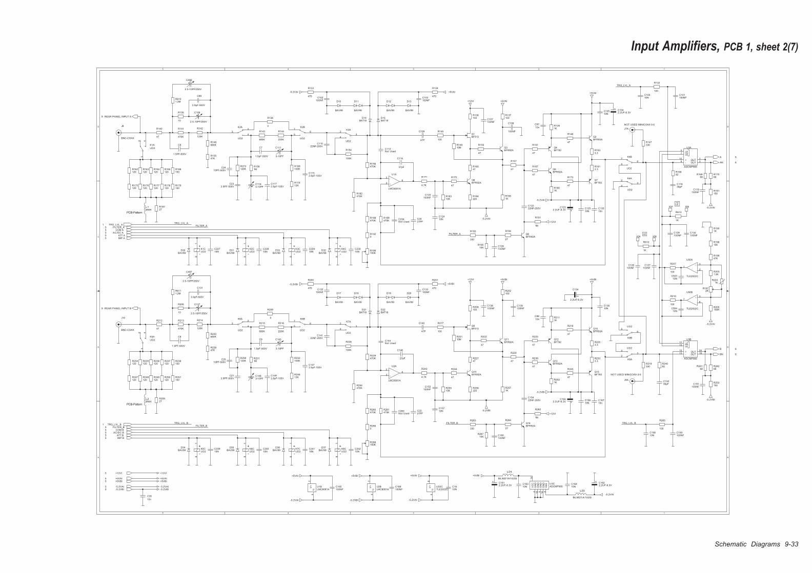
Input Amplifiers, PCB 1, sheet 2(7)
Schematic Diagrams 9-33
5
5
4
4
3
3
2
2
1
1
D D
C C
B B
A A
TRG_LVL_A
FILTER_B TRG_LVL_B
FILTER_A
FILTER_BTRG_LVL_B
TRG_LVL_A
FILTER_A
TRG_LVL_A1
TRG_LVL_B1
+12VI
+5VAI+5VBI
-5.2VAI-5.2VBI
+5VAI-5.2VAI
-5.2VAI
+5VAI+12VI
+5VAI
-5.2VAI
+12VI
-5.2VBI
-5.2VBI
+5VBI+12VI +5VBI
-5.2VBI
+12VI
-5.2VAI
-5.2VAI
-5.2VBI
-5.2VAI
+5VBI+5VAI
-5.2VAI
+5VBI
+5VBI
-5.2VBI -5.2VAI
+5VAI
+5VAI5+5VBI5
-5.2VAI5-5.2VBI5
+12VI5
IMP A5ATT A5
AC/DC A5COM A5
FILTER_A5
IMP B5ATT B5
AC/DC B5COM B5
FILTER_B5
REAR PANEL INPUT A9
REAR PANEL INPUT B9
AN 6
B 6
BN 6
A 6
LE
LE
L55
BLM21A102S
R244
47
1M
R191
R613
1K
10NC125
C9
1.5pF-500V
BAV99
D10
C143
3-10PF
10nC167
R184220
R24168
R177120
K2A
UD2
34
2
C1622.2UF-6.3V
Q13BFR92A
R181150
R248120
R163120
R188470K
R251150
R167
47
C151100NF
K7A
UD2
34
2
BAV99
D17
R16047
10NC239
R16968
BAV99
D20
K4A
UD2
34
2
-
+
U2A
LMC6081A
3
26
C12222NF-200V
R215
680K
BFT93Q7
Q5BFR92A
R237120
R212
47
C132100NF
J10
BNC-COAX
C144Not Used
X34
Q16BFR92A
BAV99D31
R148680K
R24612K
C2027PF
10NC503
+
-
K6CUD2
18
R205180K
R19510K
C140
47P
R254470K
10NC227
Q10BFR93A
K1A
UD2
342
R216
220K
C2410PF-500V
R2111K
Q14BFR92A
10NC156
R6101.2M
R173
47
R193
330
R236120
R253150
C133100NF
R247120
R1801K
C1173.9pF-100V
R182470K
R220680K
R19947K
R213
470K
10NC158
10NC240
R179150
R2333.3
10NC163
C7
1.5pF-500V
R229470K
X35
R17068
C1232.2UF-6.3V
C126100NF
+
-
K1CUD2
18
R15547K
BAV99D34
R194
27
BAV99
D12
Q2BFR93A
U1BLMC6081A
V+
7
V-
4
R223
47
R18310K
10n
C98
C496
2.5-10PF/250V
R165120
R145
100
K4B
UD2
65
7
+
-
U50A
TLE2022C
2
31
C139100NF
R189470K
C165100NF
R1901K
R17412K
R18727
10NC229
R132
100
R176120
100KR159
R207
100
R138
0
R14910M
C260Not Used
R2031.5K
10NC124
J7A
NOT USED MINICOAX-3-5
R201
470
+
-
K8CUD2
18
R1581M
R135
10
R218
47
L54
BLM21A102S
C146
27pF
C159100NF
C107100NF
R250120
10NC100 C101
100NF
BAV99
D18R6111.2M
R2241K
BAV99D33
10NC19
R196100K
R171
4.7K
R234120
R16882
X36
1M
R262R260470K
R222
47
C213.9PF-500V
R214
120K
C129100NF
BAT18D15
-
+
U1A
LMC6081A
3
26
R202100
R219330
C131
3.9pF-500V
R249120
BAT18D14
R261470K
BAV99D30
R1533.3
C11839pF
C103100NF
C152100NF
C160100NF
R235120
C1153.9pF-100V
10NC164
R24268
R258120K
R1920
C166100NF
R142
120K
R1851K
R239
47
C120100NF
+
-
K5CUD2
18
10NC105
+
-
K2CUD2
18
R157
47
10NC504
BAT18D21
R141
470K
BFT93Q15
BFT92Q4
R268100K
X37
R243
4.7K
R156470K
C1163-10PF
10n
C35
10NC241
Q3BFR92A
C1493.9pF-100V
R210
100
C102100NF
U3A
ADCMP565
LE5
LE7
+10
-9
OUT2
OUT3
R1391K
C15039pF
+
-
U50B
TLE2022C
6
57
C134
2.2UF-6.3V
R146
47
10NC230
R2311M
BAV99
D11
Q1BF513
BAV99D36
C2227PF
C127100NF
BAT18D22
R200
470
100K
R154
C99
3.9pF-500V
C234Not Used
BAV99D32
R133
470
R136100
BFT92Q12
R208100
C233.9PF-500V
R238150
C130100NF
K6B
UD2
65
7
K5A
UD2
342
BAV99D37
10NC242
R2521K
R256220
Q6BFR92A
R166150
R2253.3
C11022NF-200V
+
-
K4CUD2
18
Q9BF513
BAV99
D19
U2BLMC6081A
V+
7
V-
4
PCB-Pattern
L16NH
C6
1.5PF-500V
C108
100NF
C1483-10PF
C111
3-10PF
R143
680K
PCB-Pattern
L26NH
R137100
U3B
ADCMP565
LE17
LE15
+12
-13
OUT20
OUT19
R273120K
R217
100
R209
0
C1552.2UF-6.3V
K8A
UD2
34
2
R612
1K
R19815K
C497
2.5-10PF/250V
C128100NF
10nC135
R134
470
R245
47
R22747
R2571K
R25510K
+
-
K7CUD2
18
R25927
10NC136
R151
47
R144
220K
C15422NF-200V
BAV99D35
10NC157
R206
10
R265
100
R172
47
R26710K
C14122NF-200V
C138100NF
100KR232
Q8BFR92A
R230
47
R175120
R150
47
R162120
+
-
K3CUD2
18
R164120
C1612.2UF-6.3V
C112Not Used
R22847K
10n
C97
R264
27
R24082
R1613.3
C106
2.5-10PF/250V
R140
47
R2660
Q11BFR92A
C114
27pF
C1473.9pF-100V
U3CADCMP565G
ND
4V
CC
14
VE
E8
GN
D1
8
GN
D6
GN
D1
6
J8
BNC-COAX
U50CTLE2022C
V+
8
V-
4
J9A
NOT USED MINICOAX-3-5
BAV99
D13
C109
47P
R1972K
R22110M
C2510PF-500V
K2B
UD2
65
7
R263
330
100K
R226
R147330
K8B
UD2
65
7
C119100NF
R178120
K6A
UD2
34
2
K3A
UD2
34
2
C8
1.5PF-500V
10NC228
C1042.2UF-6.3V
C137
2.5-10PF/250V

9-34 Schematic Diagrams
This page is intentionally left blank.
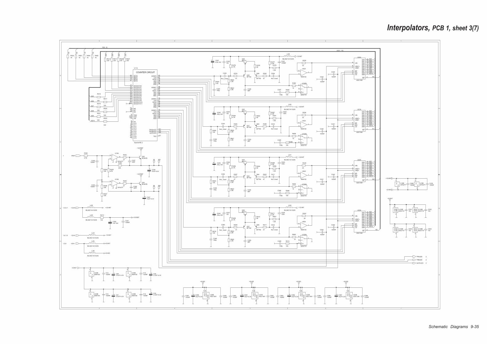
Interpolators, PCB 1, sheet 3(7)
Schematic Diagrams 9-35
5
5
4
4
3
3
2
2
1
1
D D
C C
B B
A A
AD10
AD6
AD5
AD8
AD7
AD9
R[0..3]
R0
R1
R2
R3
AD[1..10]
AD
1
AD
2
AD
3
AD
4
R0
AD1AD2AD3AD4AD5AD6AD7AD8AD9AD10
R1
AD1AD2AD3AD4
AD7AD6AD5
AD8AD9AD10
R2
AD2AD1
AD3
AD5AD4
AD6
AD8AD7
AD9AD10
R3
AD2AD1
AD5AD4AD3
AD7AD6
AD8AD9AD10
VREF1
+12VINT
+12VREF
-12VINT
+5VINT
+5VAD
+12VREF
+12VREF
-12VINT
+12VINT
+5VINT
+12VINT
+12VINT
+12VINT
+12VINT
+5VINT
+5VAD+5VAD+5VAD+5VAD
+12VA1,5,6,7
-12VA1,6,7,8
+5VA1,5,6
TRALED 2
TRBLED 2
GATELED 2
C351100NF
R481
1KQ28BF513
R402
47
R4112.2K
C13100NF
C321100NF
C336
Not_Used
R40610K
L61
BLM21A102S
R6442.2K
BFT92Q29
C363100NF
-
+
U18A
OPA277
3
26
1 8
R417
47
R403100
R522
330
U135A
ADG719
8
21
6
R405
47
U44BKM4100
V+
5
V-
2
U23A
ADC1061
INT2
S/H3
RD4
CS5
VREF-7
VIN8
VREF+9
DB218
DB119
DB020
DB614
DB515
DB416
DB317
DB713
DB812
DB911
C36115UF-6.3V
R3964.7K
U20BADC1061V
CC
1
+V
CC
6
GN
D10
C327
100p
C36415UF-6.3V
-
+
U45A
KM4100
3
41
C329
100p
R656
1.5K
C341
100NF
10nC534
R385
47
L24
BLM21A102S
C362100NF
R507330
R3754.7K
C312.2UF-6.3V
BFT92
Q59
R6402.2K
C33368P
R657
1.5K
10nC525
R40710K
BFT92Q37
C33915UF-6.3V
R505
1K
Q32BC847B
L22
BLM21A102S
L62
BLM21A102S
R65282
C14100NF
Q30BF513
BFT92Q31
C369100NF
L23
BLM21A102S
C356
Not_Used
L60
BLM21A102S
C34715UF-6.3V
C357100NF
U133BADG719V
DD
4
GN
D3
R37682
R521
330
U133A
ADG719
8
21
6
R6422.2K
U42BKM4100
V+
5
V-
2
R4084.7K
Q36BF513
R6412.2K
10nC532
U22A
ADC1061
INT2
S/H3
RD4
CS5
VREF-7
VIN8
VREF+9
DB218
DB119
DB020
DB614
DB515
DB416
DB317
DB713
DB812
DB911
R6332.2K
C34468P
C359100NF
C323
100NF
R41082
R528
22
C338100p
R40047K
C3501uF-16V
BFT92Q34
R382
100
10nC527
C368100NF
R519
330
R378
47
10nC526
C509
Not Used
R40482
R398
100
R3772.2K
10nC531
C5296.8u-16V
C322.2UF-6.3V
C340100NF
-
+
U19A
OPA277
3
26
1 8
X4R659
10
C324
100NF
C353
100NF
C512
Not Used
R513330
C331
100NFBFT92
Q63
U135BADG719V
DD
4
GN
D3
C15100NF
R414
100
C349
100p
C346
100p
C522100n
R485
1K
R395
33K
R520
330 R391
1.5K
R381100
C328100p
U134BADG719V
DD
4
GN
D3
COUNTER CIRCUIT
U11A
SpartanIIE-2
ERRP063
SH056
CS057
RD058
SH181
CS182
RD183
ERRP270
SH286
CS287
RD288
ERRP373
SH393
RES059
ERRP168
RES184
RES289
CS394
RD395
RES396
RDY060
RDY175
RDY274
RDY397
ADCDATA027
ADCDATA129
ADCDATA230
ADCDATA331
ADCDATA433
ADCDATA534
ADCDATA635
ADCDATA736
ADCDATA840
ADCDATA941
ADCDATA1043
ADCDATA1144
TRIGALED191
TRIGBLED192
GATELED193
M052
M150
M254
TMS2
TCK207
TDI159
TDO157
U98
U109
U1115
U1216
U1322
U1417
U1518
U1623
U1724
U1861
U1962
U2064
U2169
U2271
U2380
R383
47
C322100p
C325
Not_Used
U22BADC1061V
CC
1
+V
CC
6
GN
D10
U43BKM4100
V+
5
V-
2
R397
47
U132BADG719V
DD
4
GN
D3
C365100NF
R6342.2K
R660
10
C335100NF
R539
22
U18BOPA277
V+
7
V-
4
R517
330
R386
100
C360100NF
R413
100
C5286.8u-16V
C342
100NF
R389
47
R409
47R416100
U20A
ADC1061
INT2
S/H3
RD4
CS5
VREF-7
VIN8
VREF+9
DB218
DB119
DB020
DB614
DB515
DB416
DB317
DB713
DB812
DB911
C523100n
10nC533
R511330
R6432.2K
X53
C524100n
R392
4.7K
C33710PF
C292.2UF-6.3V
-
+
U43A
KM4100
3
41
C34510PF
U21A
ADC1061
INT2
S/H3
RD4
CS5
VREF-7
VIN8
VREF+9
DB218
DB119
DB020
DB614
DB515
DB416
DB317
DB713
DB812
DB911
R524
22
R484
1K
R393
47
Q35BC847B
C12100NF
C330
100NF
-
+
U42A
KM4100
3
41
C510
Not Used
L25
BLM21A102S
C511
Not Used
C352
100NF
R540
22
U134A
ADG719
8
21
6
C334
Not_Used
BFT92
Q64
R658
10
C5076.8u-16V
C366100NF
R3992.2K
U132A
ADG719
8
21
6
R3872.2K
U45BKM4100
V+
5
V-
2
C348100p
U21BADC1061V
CC
1
+V
CC
6
GN
D10
R6452.2K C355
68P
R515
330
X54
X3
C32668P
C35815UF-6.3V
C370100NF
R3844.7K
C36715UF-6.3V
R39415K
L59
BLM21A102S
Q33BF513
U19BOPA277
V+
7
V-
4
-
+
U44A
KM4100
3
41
BFT92
Q65
L26
BLM21A102S
R380
10
R508330
C5306.8u-16V
U23BADC1061V
CC
1
+V
CC
6
GN
D10
R379
1.5K
C302.2UF-6.3V
10nC332
R390100

9-36 Schematic Diagrams
This page is intentionally left blank.
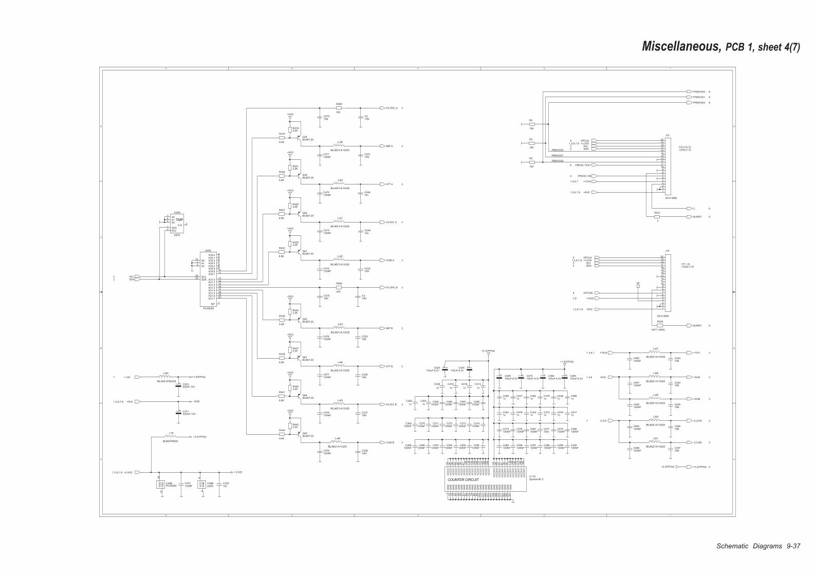
Miscellaneous, PCB 1, sheet 4(7)
Schematic Diagrams 9-37
5
5
4
4
3
3
2
2
1
1
D D
C C
B B
A A
PREKOD2
PREKOD1
PREKOD0
+5VD
+3.3VD
+5VD
+5VD
+5VD
+5VD
+5VD
+5VD
+5VD
+5VD
+1.8VFPGA
+3.3VFPGA
+3.3VFPGA
+1.8VFPGA
+3.3VFPGA
SDA2SCL2
+5VD1,2,6,7,8
+3.3VD1,2,6,7,8
OPCLK6+3.3VD1,2,6,7,8
SCL2SDA2
PRESC ON6
+5VD1,2,6,7,8
+12VA1,4,6,7
PRESC TEST6
+5VD1,2,6,7,8
OPTION6
OPCLK6+3.3VD1,2,6,7,8
SCL2SDA2
+12VA1,4,6,7
+5VA1,4,6
-5.2VI7
+15VD7,8
IMP A 3
ATT A 3
AC/DC A 3
COM A 3
FILTER_B 3
BURST 6
C 6
BURST 6
FILTER_A 3
+12VI 3
+5VAI 3
+5VBI 3
-5.2VAI 3
-5.2VBI 3
AC/DC B 3
IMP B 3
ATT B 3
COM B 3
PREKOD0 8
PREKOD2 8
PREKOD1 8
+1.8V7
+3.3VFPGA 2
PRES CAL ERCONNECT OR
OPT I ONCONNECT OR
10nC249
R4182.2K
R444
6.8K
C292100NF
C477100NF
C5801n
R4432.2K
C291100NF
L50
BLM21A102S
C297100NF
C3431n
C575100uF-6.3V
R4372.2K
L16
BLM41P800S
R565
330
C271100NF
10NC238
C481100NF
L51
BLM21A102S
C420
1n
10NC3
C473100NF
C272100NF
R428
NOT USED
10NC2
R4402.2K
C478100NF
C392
1n
R435
6.8K
C371220UF-10V
Q45BC807-25
C274100NF
C5661n
L43
BLM21A102S
R419
6.8K
J15
2X10 SMD
123456789
1011121314151617181920
C293100NF
L47
BLM21A102S
10nC320
C5371n
U40BPCA9555V
DD
24
VS
S1
2
Q44BC807-25
C372100NF
C273100NF
L49
BLM21A102S
C3731n
C384100uF-6.3V
C299100NF
C267100NF
Q39BC807-25
10NC237
10NC245
10NC244
10NC475
L46
BLM21A102S
TMP
U39A
LM75
SDA1
SCL2
A07
A16
A25
O.S.3
C268100NF
R4342.2K
C474100NF
C300100NF
C413
1n
C253220uF-10V
R438
6.8K
C298100NF
R2
10K
C567100NF
R422
6.8K
C486100NF
C275100NF
10NC246
L40
BLM21A102S
C479100NF
C5821n
Q40BC807-25
C423100uF-6.3V
10NC231
R4
10K
L44
BLM21A102S
C5761n
C390100uF-6.3V
10NC247
10NC236
C472100NF
C480100NF
R4212.2K
U39BLM75G
ND
4V
CC
8
C3021n
Q42BC807-25
X5
C270100NF
C295100NF
R4262.2K
C266100NF
Q41BC807-25
C418
1n
COUNTER CIRCUITU11DSpartanIIE-2
GN
D1
GN
D1
2
GN
D1
9
GN
D2
5
GN
D3
2
GN
D3
9
GN
D5
1
GN
D6
5
GN
D7
2
GN
D7
9
GN
D8
5
GN
D9
2
GN
D1
03
GN
D1
17
GN
D1
24
GN
D1
31
GN
D1
37
GN
D1
44
GN
D1
58
GN
D1
70
GN
D1
77
GN
D1
83
GN
D1
90
GN
D1
97
VC
CO
13
VC
CO
26
VC
CO
38
VC
CO
53
VC
CO
66
VC
CO
78
VC
CO
91
VC
CO
10
5
VC
CO
11
8
VC
CO
13
0
VC
CO
14
3
VC
CO
15
6
VC
CO
17
1
VC
CO
18
4
VC
CO
19
6
VC
CO
20
8
VC
CIN
T14
VC
CIN
T28
VC
CIN
T37
VC
CIN
T67
VC
CIN
T76
VC
CIN
T90
VC
CIN
T11
9
VC
CIN
T12
8
VC
CIN
T14
2
VC
CIN
T17
2
VC
CIN
T18
6
VC
CIN
T19
5
R441
6.8K
C296100NF
R564
330
C265100NF
R427
6.8K
C483100NF
C280100NF
C269100NF
R431
0
C276100NF
C3791n
J16
2X10 SMD
123456789
1011121314151617181920
10nC248
R4302.2K
C425100uF-6.3V
Q38BC807-25
10NC232
L41
BLM21A102S
C5771n
L48
BLM21A102S
Q43BC807-25
C5791n
C539100uF-6.3V
C476100NF
C471100NF
10NC243
C294100NF
C277100n
10NC235
L39
BLM21A102S
C419
1n
C290100NF
C279100NF
L45
BLM21A102S
C484100NF
C391
1n
10NC470
R432
6.8K
R3
10K
U40A
PCA9555
A021
A12
A23
SCL22
SDA23
I/O0.04
I/O0.15
I/O0.26
I/O0.37
I/O0.48
I/O0.59
I/O0.610
I/O0.711
I/O1.013
I/O1.114
I/O1.215
I/O1.316
I/O1.417
I/O1.518
I/O1.619
I/O1.720
INT1
C289100NF
L42
BLM21A102S
L20
BLM41P800S
C5381n

9-38 Schematic Diagrams
This page is intentionally left blank.
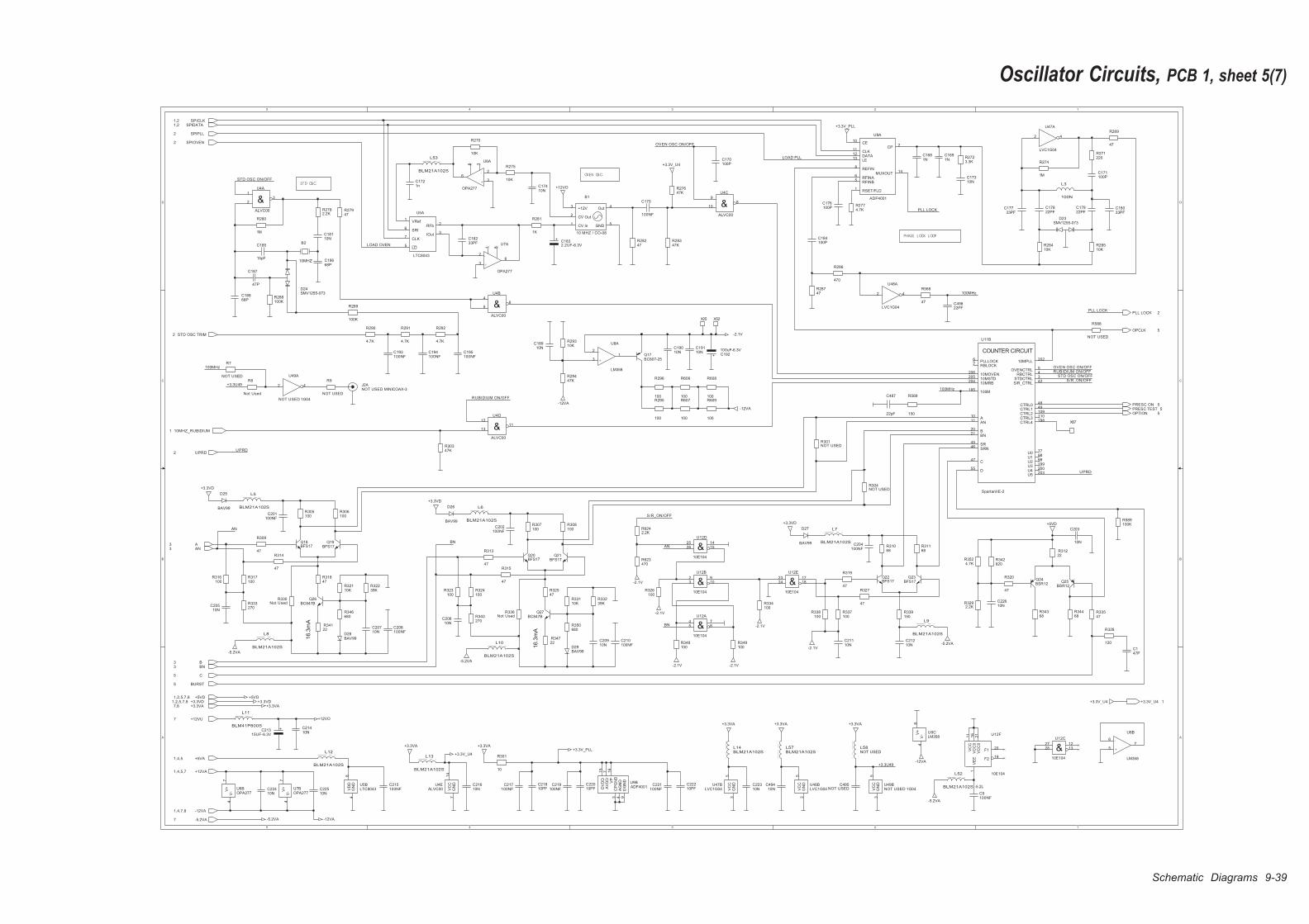
Oscillator Circuits, PCB 1, sheet 5(7)
Schematic Diagrams 9-39
5
5
4
4
3
3
2
2
1
1
D D
C C
B B
A A
STD OSC ON/OFF
OVEN OSC ON/OFF
RUBIDIUM ON/OFF
PLL LOCK
LOAD PLL
AN
AN
BN
OVEN OSC ON/OFFRUBIDIUM ON/OFF
STD OSC ON/OFF
100MHz
-5.2L
100MHz
+3.3U49
+3.3U49
S/R_ON/OFF
S/R_ON/OFF
BN
100MHz
LOAD OVEN
PLL LOCK
UPRD
UPRD
+3.3V_U4 1
10MHZ_RUBIDIUM1
+12VO
-2.1V
+3.3V_PLL+3.3V_U4
+3.3V_U4
+12VO
+3.3V_PLL
+3.3VD
-5.2VA
+3.3VD
-5.2VA
-2.1V
-2.1V -2.1V
-2.1V
+5VD+3.3VD
-5.2VA
+3.3VA +3.3VA
+3.3VA
-5.2VA
-12VA
-12VA
-12VA
-2.1V
+3.3V_U4
+3.3VA +3.3VA
-2.1V
-12VA-5.2VA
+3.3VA
+5VD+3.3VD
STD OSC TRIM2
SPICLK1,2SPIDATA1,2
AN3A3
PRESC ON 5PRESC TEST 5OPTION 5
OPCLK 5
C5
+12VU7
B3
+12VA1,4,5,7
+5VA1,4,5
-12VA1,4,7,8
-5.2VA7
+3.3VA7,8+3.3VD1,2,5,7,8
BURST5
BN3
+5VD1,2,5,7,8
SPIPLL2
SPIOVEN2
PLL LOCK 2
UPRD2
S T D OS C.
OVEN OS C.
16.3
mA
16.3
mA
PHAS E L OCK L OOP
C21810PF
C1681N
R33239K
C202100NF
R281
1K
U48BLVC1G04V
CC
5
GN
D3
R309
47
BAV99
D26
R568
47
L8
BLM21A102S
C17733PF
R31847
R334100
R28747
L10
BLM21A102S
C5100NF
10NC190
C185
15pF
R270
10K
R275
10K
R29447K
R32110K
U5A
LTC8043
VRef1
RFb2
SRI6
CLK7
LD5
IOut3
10NC211
L14BLM21A102S
C495NOT USED
R336Not Used
R32239K
&U12E
10E104
2324 18
17
C22210PF
L5
BLM21A102S
C22010PF
L52
BLM21A102S
10NC189
10NC225
10NC174
&ALVC00
U4B
64
5
C171100P
R609
100
R314
47
R306100
Q26BC847B
C18233PF
J2ANOT USED MINICOAX-3
10N
C203
R9
NOT USED
R304NOT USED
10NC181
BAV99D28
C210100NF
Q20BFS17
R296
100
C18668P
C175
100NF
R34368
R29310K
L12
BLM21A102S
L13
BLM21A102S
R319
47
C49822PF
C195100NF
1M
R274
R30347K
R338100
R342820
R337100
C176100P
R34122
R315
47
BAV99
D27
10NC207
R3524.7K
R27647K
C1832.2UF-6.3V
&U12A
10E104
45 8
7
10NC226
C21315UF-6.3V
L57BLM21A102S
R32547
BAV99D29
C201100NF
10NC209
R2723.3K
U7BOPA277
V+
7
V-
4
C184100P
R291
4.7K
C208100NF
Q22BFS17
R320
47
X52
&ALVC00
U4C
89
10
10NC214
R31068
R348100
R3292.2K
Q25BSR12
Q24BSR12
10NC494
&U12D
10E104
2526 15
14
R351
10
R295
100
R34468
R346680
10NC206
D24SMV1255-073
U9A
ADF4001
CP2
RSET/FLD1
RFINB5
RFINA6
REFIN8
CLK11
DATA12
LE13
MUXOUT14
CE10
L58NOT USED
10NC223U47B
LVC1G04 VC
C5
GN
D3
R608
100
BAV99
D25
X67
Q27BC847B
R588
NOT USED
R33547
C170100P
R307100
R326100
U49BNOT USED 1G04V
CC
5
GN
D3
10NC173
R308100
R28247
10NC212
R34722
Q21BFS17
U49A
NOT USED 1G04
2 4
-
+
U7A
OPA277
3
26
1 8
R349100
&U12B
10E104
23 10
9
R333270
R8
Not Used
R292
4.7K
L9
BLM21A102S
U6BOPA277
V+
7
V-
4
COUNTER CIRCUIT
U11B
SpartanIIE-2
PLLLOCK6
RBLOCK7
10MOVEN206
10MSTD205
10MRB204
100M185
10MPLL202
OVENCTRL5
RBCTRL4
STDCTRL3
S/R_CTRL42
A10
AN11
B20
BN21
SR45
SRN46
C47
D55
CTRL048
CTRL149
CTRL2109
CTRL3110
CTRL4188
U077
U198
U299
U3199
U4200
U5203
R2774.7K
C17822PF
Q19BFS17
U4EALVC00 G
ND
7V
CC
14
10NC216
R33110K
B1
10 MHZ / CO-08
CV In1
CV Out2
+12V3
Out4
GND5
R350680
R271220
U8CLM358
V+
8
V-
4
+
-
U8A
LM358
2
31
R27947
R31168
Q18BFS17
C187
47P
C193100NF
U9BADF4001
CP
GN
D3
AG
ND
4
AV
DD
7
DG
ND
9
DV
DD
15
VP
16
R330Not Used
L11
BLM41P800S
R6242.2K
C194100NF
R28410K
R327
47
C17922PF
-
+
U6A
OPA277
3
26
18
&ALVC00
U4A
31
2
C1691N
B2
10MHZ
U12F
10E104
VE
E1
VC
C0
16
F219
VC
C1
1
F120
VC
C0
21
R317100
L6
BLM21A102S
C204100NF
R569
150
R313
47
L7
BLM21A102S
R31222
L3
100N
R316100
10NC205
R607
100
R28510K
R286
470
R340270
C219100NF
R323100
C18033PF
C147P
C18868P
R606
100
R623470
R301NOT USED
Q23BFS17
R339150
R324100
X25
C487
22pF
L53
BLM21A102S
10NC191
&U12C
10E104
2728 13
12
C1721n
Q17BC807-25
10NC224
C192100uF-6.3V
U5BLTC8043V
DD
8
GN
D4
U47A
LVC1G04
2 4
100KR589
R305100
1M
R280
C221100NF
R328
120
D23SMV1255-073
100K
R289
C215100NF
R7
NOT USED
C217100NF
R269
47
R2782.2K
U48A
LVC1G04
2 4
100KR288
R290
4.7K
R28347K
+
-
U8B
LM358
6
57
&ALVC00
U4D
1112
13

9-40 Schematic Diagrams
This page is intentionally left blank.
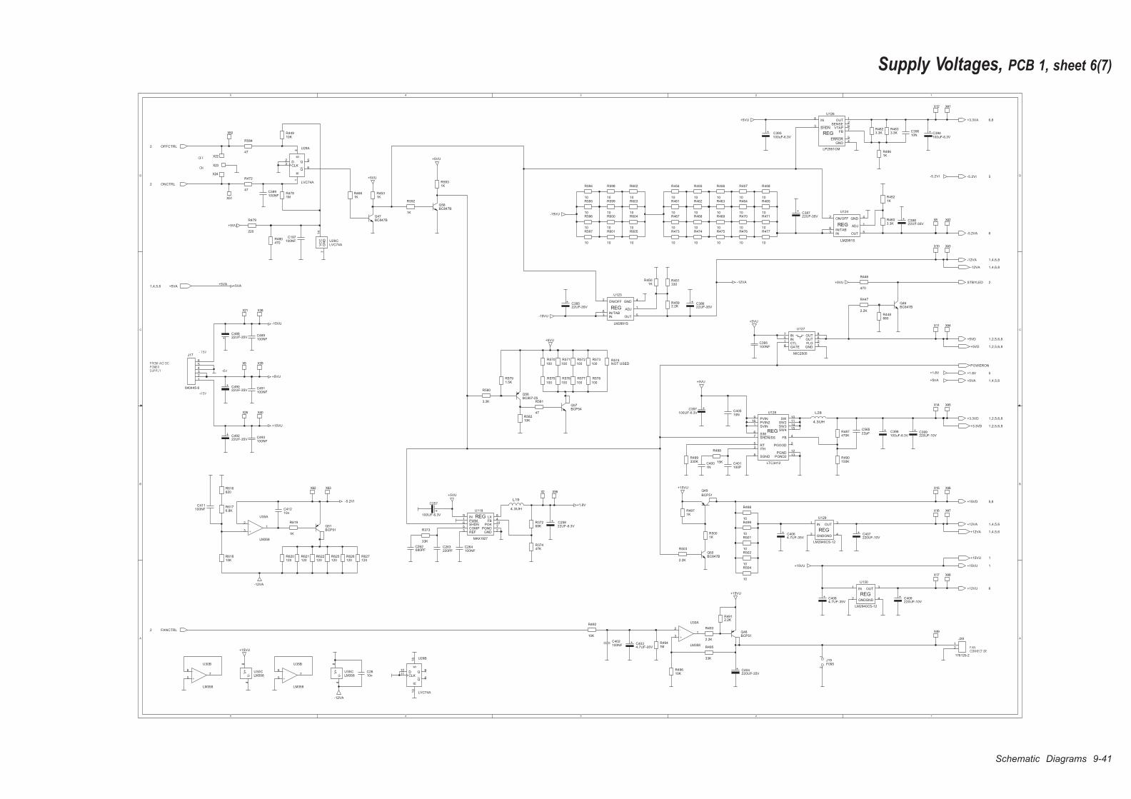
Supply Voltages, PCB 1, sheet 6(7)
Schematic Diagrams 9-41
5
5
4
4
3
3
2
2
1
1
D D
C C
B B
A A
+5VA
POWERON
+5VD 1,2,5,6,8
+3.3VD 1,2,5,6,8
+12VA 1,4,5,6
-12VA 1,4,6,8
+5VA1,4,5,6
+15VU 1
+5VU
-15VU
+15VU
-12VA
-5.2VI
+5VA
+5VU
+5VU
+5VU
+5VU
+5VU
+5VU
+5VU
-15VU
-15VU
+15VU
+15VU
+15VU
+5VU
+15VU
-12VA
-5.2VI
+5VA
-12VA
+1.8V
+5VU
+1.8V
OFFCTRL2
ONCTRL2
FANCTRL2
-5.2VA 6
-12VA 1,4,6,8
+5VD 1,2,5,6,8
+3.3VA 6,8
+3.3VD 1,2,5,6,8
+15VU 1
+15VD 5,8
+12VA 1,4,5,6
+12VU 6
STBYLED 2
+5VA 1,4,5,6
-5.2VI 5
+1.8V 5
F ROM AC/ DCPOWERS UPPL Y
- 15V
+5V
+15V
F ANCONNECT OR
ON
OFF
REG
U129
LM2940CS-12
IN1
OUT3
GND2
GND4
R469
10
C395100NF
+
-
U35B
LM358
6
57
+
-
U30A
LM358
2
31
R578
100
+
-
U30B
LM358
6
57
X12
C398100uF-6.3V
C402100NF
X50
R4501K
REG
U123
LM2991S
IN3
OUT5
ADJ1
GND4
ON/OFF2
IN/TAB6
C257
100UF-6.3V
R488
15K
R468
10
X43
R4592.2K
X17
R4861K
1MR494
U30CLM358
V+
8
V-
4
C4001N
R602
10
X8
C397100UF-6.3V
X38
X10
Q50BC847B
C491100NF
R594
10
Q56BC807-25
Q57BCP54
R625120
R476
10
X51
X24
R487470K
R504
10
X62
X44
C48822UF-35V
C264100NF
R502
10
10nC26
R480470
U127
MIC2505
CTL1
FLG2
GATE4
GND3
IN7
IN5
OUT8
OUT6
R464
10
U29B
LVC74A
D12
CLK11
S1
0R
13
Q9
Q8
R498
10
R44910K
R447
2.2K
R479
220
C399220UF-10V
R455
10
C411100NF
C38822UF-35V
R575
100
R6176.8K
R58210K
X56
330KR489 R490
150K
U35CLM358
V+
8
V-
4
REG
U130
LM2940CS-12
IN1
OUT3
GND2
GND4
X45R581
47
R598
10
U29A
LVC74A
D2
CLK3
S4
R1
Q5
Q6
R599
10
R37268K
R471
10REG
U124
LM2991S
IN3
OUT5
ADJ1
GND4
ON/OFF2
IN/TAB6
R626120
R37447K
X16
R456
10
X39
U29CLVC74AV
CC
14
GN
D7
J19F095
12
REG
U126
LP2951CM
IN8
OUT1
SHDN3
GND4
SENSE2
ERROR5
VTAP6
FB7
R463
10R467
10
R462
10
R49610K
X46
REG
U128
LTC3412
PVIN9
PVIN216
SVIN1
FB4
PGND12
PGND213
SGND8
S/M6
SHDN/SS7
PGOOD2
RT5
ITH3
SW10
SW211
SW314
SW415
X22
J17
640445-6
123456
X23
R457
10
Q48BCP51
R571
100
R576
100
R4823.3K
R373
33K
R572
100
R597
10
R446
470
R603
10R600
10
R584
47
R4603.3K
X63
C489100NF
X40
R592
1K
X21
R4521K
C25822UF-6.3V
C56522pF
R4971K
X14
X47
R499
10
R5791.5K
1MR478
R574NOT USED
R5931K
R627120
R493
2.2K
R616820
R458
10
R492
10K
L19
4.3UH
R472
47
C407220UF-10V
R474
10
R580
3.3K
C38522UF-35V
X26
R619
1K
R621120
10NC405
R570
100
Q51BCP51
R577
100
C49022UF-35V
R454
10
X2
R475
10
R595
10
X15
+
-
U35A
LM358
2
31
C393100uF-6.3V
Q58BC847B
10nC412
C409220UF-10V
R4833.3K
X48
Q47BC847B
R473
10
X41
R465
10
C389100NF
R596
10
C38722UF-35VR470
10
R4912.2K
R601
10
C4084.7UF-35V
R4661K
L28
4.3UH
R495
33K
X9
R501
10
Q49
BCP51
R5001K
R4531K
10NC396
C263220PF
C262680PF
R573
100
R604
10
X49
R451330
Q46BC847B
REG
U118
MAX1927
IN9
SHDN6
COMP5
REF3
PWM1
GND2
POK10
FB4
LX8
PGND7
C4064.7UF-35V
C38622UF-35V
R461
10
R622120
X42
R605
10
X11
J28
176125-2
12
C493100NF
C197100NF
C401100P
R448680
R620120
C4034.7UF-35V
C404220UF-35V
R61810K
C49222UF-35V
R503
2.2K
C394100uF-6.3V
R477
10

9-42 Schematic Diagrams
This page is intentionally left blank.
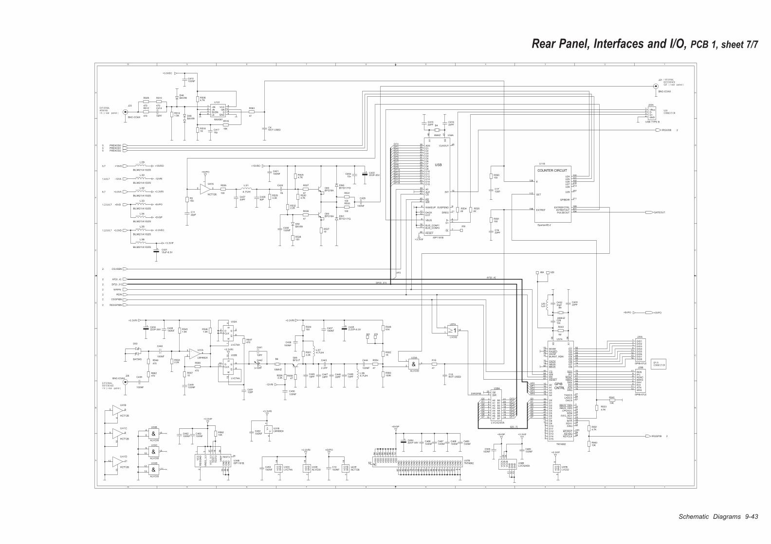
Rear Panel, Interfaces and I/O, PCB 1, sheet 7/7
Schematic Diagrams 9-43
10
10
9
9
8
8
7
7
6
6
5
5
4
4
3
3
2
2
1
1
H H
G G
F F
E E
D D
C C
B B
A A
G0G1G2
G6G7
G0G1G2
G5G6G7
G3
G5G4
G3G4
G[0..7]
DIRGPIB
DF1
DF5
DF7
DF4
DF0
DF2DF3
AF2AF3AF4
AF0
DF1
DF10
DF12DF11
DF8
DF4
DF6DF7
DF13
DF2
DF0
DF[0..31]
DF5
DF14
DF9
DF3
DF15
DF6
AF1AF0
AF[0..4]
+5VPO
GATEOUT
+15VRO
-12VRI
+3.3VRI
+3.3VEC
+3.3VIF
+5VPO
+5VGP
+3.3VEC
+3.3VIF
+15VRO
-12VRI
+3.3VRI +3.3VRI
+3.3VRI
+5VGP +3.3VIF
+5VGP
+3.3VIF
+3.3VRI
+5VPO
+5VPO
+5VPO
+3.3VRI
+3.3VIF
CSUSBN2
RESGPIBN2
CSGPIBN2
RDN2
WRFN2
DF[0..31]2
+15VD5,7
-12VA1,4,6,7
+3.3VA6,7
+3.3VD1,2,5,6,7
+5VD1,2,5,6,7
IRQGPIB 2
IRQUSB 2
AF[0..4]2
PREKOD25PREKOD15PREKOD05
I NT ERNALREFERENCEOUT ( r ear panel )
EXT ERNALARMI NGI N ( r ear panel )
US BCONNECT OR
EXT ERNALREF ERENCEI N ( r ear panel )
GP I BCONNECT OR
R590150
R531
100
U57BLVC02G
ND
3V
CC
5
B4
6MHZ
L384.7UH
R5513.3K
R547470
C469100NF
C41622PF
C44833PF
U41EHCT126V
CC
14
GN
D7
U131
MAX961
+IN1
-IN2
SHDN3
LE4
VCC8
QN7
Q6
GND5
R5451.5K
R555
470
R5322.2K
10nC28
C429
100NF
C410100NF
BAT54S
D53
R53710
C43422UF-35V
C18NOT USED
C452100NF
R5064.7K
C41522PF
BAV99D46
U38A
LVC424 5A
OE22
DIR2
A03
A14
A25
A36
A47
A58
A69
A710
B021
B120
B219
B318
B417
B516
B615
B714
USB
U34A
ISP1181B
AD038
D135
D234
D333
D432
D531
D630
D729
D828
D927
D1024
D1123
D1222
D1321
D1420
D1519
A039
ALE42
CS43
RD40
WR41
INT15
SUSPEND9
WAKEUP8
DREG11
DACK12
EOT10
BUS_CONF118
BUS_CONF017
GL7
X1
48
X2
47
VBUS6
D-4
D+5
RESET44
CLKOUT45
10MHZ
B6
C43115uF-6.3V
U34BISP1181B
VC
C1
VC
C_3
,337
TE
ST
113
TE
ST
214
TEST316
GN
D25
GN
D36
GN
D46
RE
GG
ND
2
VR
EG
_3
,33
VR
EF
26
C466100NF
R591150
U32CLVC74AV
CC
14
GN
D7
R5254.7K
R583
47
C4NOT USED
C467100NF
L631uH
R541
10K
R509
470
C4352.2UF-6.3V
U32B
LVC74A
D12
CLK11
S1
0R
13
Q9
Q8
U38BLVC4245AV
CC
A1
VC
CB
23
VC
CB
24
GN
D1
1
GN
D1
2
GN
D1
3
C44515PF
C43322PF
R53522
C42882P
R5582.2K
X18
J25B
GPIB-57LE
REN17
IFC9
NDAC8
NRFD7
DAV6
EOI5
ATN11
SRQ10
C450
100NF
GPIBCNTRL
U37A
TNT4882
DRQ32
RDY138
X0
95
X1
96
A015
A116
A217
A318
A419
D039
D142
D243
D344
D446
D547
D649
D750
D811
D910
D109
D117
D126
D135
D143
D152
CS55
WR64
RD63
RESET67
INTR34
TRIG23
IO192
IO291
IO389
IO488
IO580
IO677
IO774
IO871
SRQ76
ATN73
EOI85
DAV84
NRFD82
NDAC81
IFC79
REN70
ABUS14
BBUS62
DACK33
BURST_RDN31
FIFO_RDY30
SWAP29
REM28
ABUS_OEN20
BBUS_OEN1
PAGED26
CPUACC22
MODE53
TADCS21
LADCS66
DACS51
KEYRST100
KEYCLK98
KEYDQ99
Q55BFS17
&ALVC00
U33D
1112
13
R56210K
C42222UF-35V
1M
R543
D50BYD17G
J25A
GPIB-57LE
DIO11
DIO22
DIO33
DIO44
DIO513
DIO614
DIO715
DIO816
10nC454
L29
BLM21A102S
R5521K
L36
BLM21A102S
R5141.5K
U31BLMH6624
V+
7
V-
4
J22A
USB TYPE B
VBus1
D-2
D+3
GND4
R538120
C449100NF
NC52
U37BTNT4882V
DD
12
VD
D2
4V
DD
36
VD
D4
0V
DD
58
VD
D6
9
VD
D6
0
VD
D8
7V
DD
94
GN
D4
GN
D8
GN
D13
GN
D27
GN
D25
GN
D35
GN
D37
GN
D41
GN
D45
GN
D48
GN
D54
GN
D56
GN
D57
GN
D59
GN
D61
GN
D65
GN
D68
GN
D72
GN
D75
GN
D78
GN
D83
GN
D86
GN
D90
GN
D93
GN
D97
R55715
R53422
C41710p
COUNTER CIRCUIT
U11E
SpartanIIE-2
GET112
E126
EXTREF198
U24100
U25101
U26102
U27108
U28113
U29187
EXTREFCTRL189
INTREFOUT201
PULSEOUT194
GPIBDIR111
L30
BLM21A102S
U 41C
HCT126
9 8
10
C440
100NF
C44733PF
R523
4.7K
&ALVC00
U33A
31
2
C443
2.2PF
U41B
HCT126
5 6
4
R5532.2K
C44615PF
C463100NF
R549
470
R512
470
R516
15K
D51BYD17G
C465100NF
R56310K
C414
10PF
R54891K
C436100NF
L31
4.7UH
U33EALVC00G
ND
7V
CC
14
L374.7UH
L34
BLM21A102S
U32A
LVC74A
D2
CLK3
S4
R1
Q5
Q6
C441
10PF
R5461.5K
R5150
X20
X19
R662470
C468100NF
1
U57A
LVC02
2
14
J21
BNC-COAX
X61
C462100NF
R16
47
R55947
R5614.7K
+
-
U31A
LMH66242
36
&ALVC00
U33B
64
5
Q54BFG16A
R526
100
X64
J26BNC-COAX
Q53BFG16A
R544100
L32
BLM21A102S
R536
47
C437100NF
C430100NF
BAV99D48
R533
100
C424
1NR5304.7K
R5181K
C421100NF
U 41D
HCT126
12 11
13
C46422UF-35V
U41A
HCT126
2 3
1
C505100NF
100KR560
C451100P
C17100P
R5293.3KC427
33PF
C438
100NF
&ALVC00
U33C
89
10
R527
47
J23
BNC-COAX
L33
BLM21A102S
C439
100NF
C442
3-10PF
C453100NF
R510
470
C444
100NF
L35
BLM21A102S
C43233pF
R554
47
C1122pF
BAV99D52
C10100NF
C1622PF
40MHZ
B5
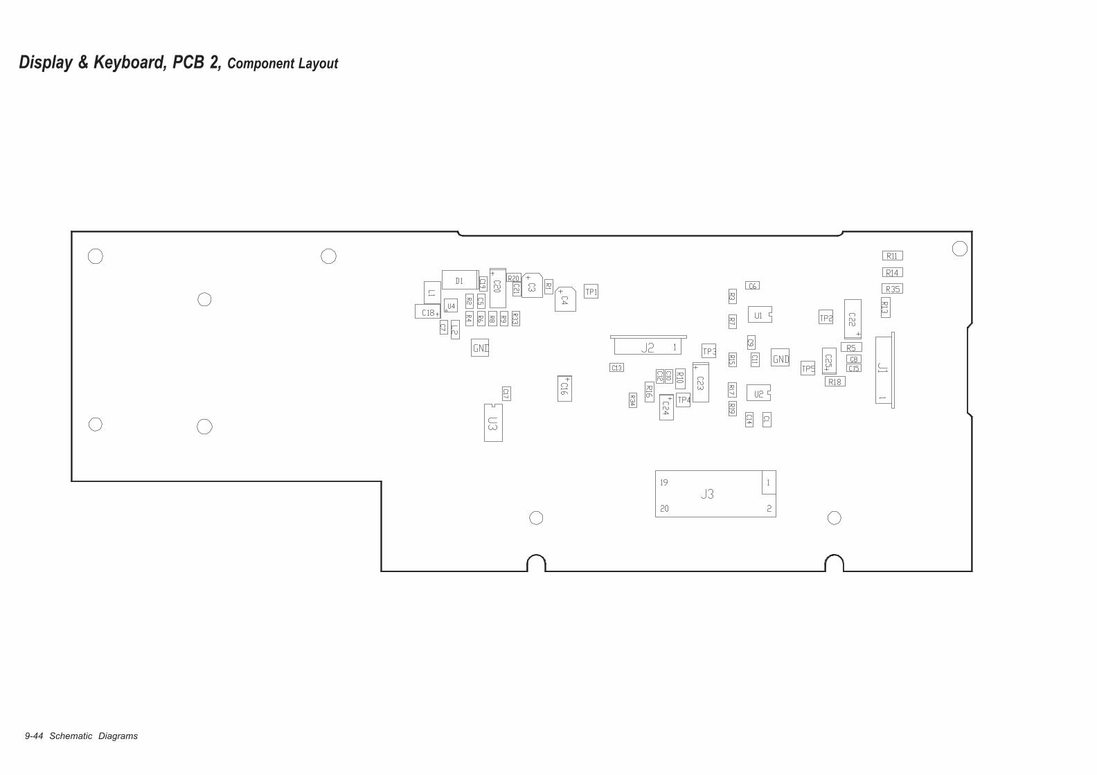
Display & Keyboard, PCB 2, Component Layout
9-44 Schematic Diagrams
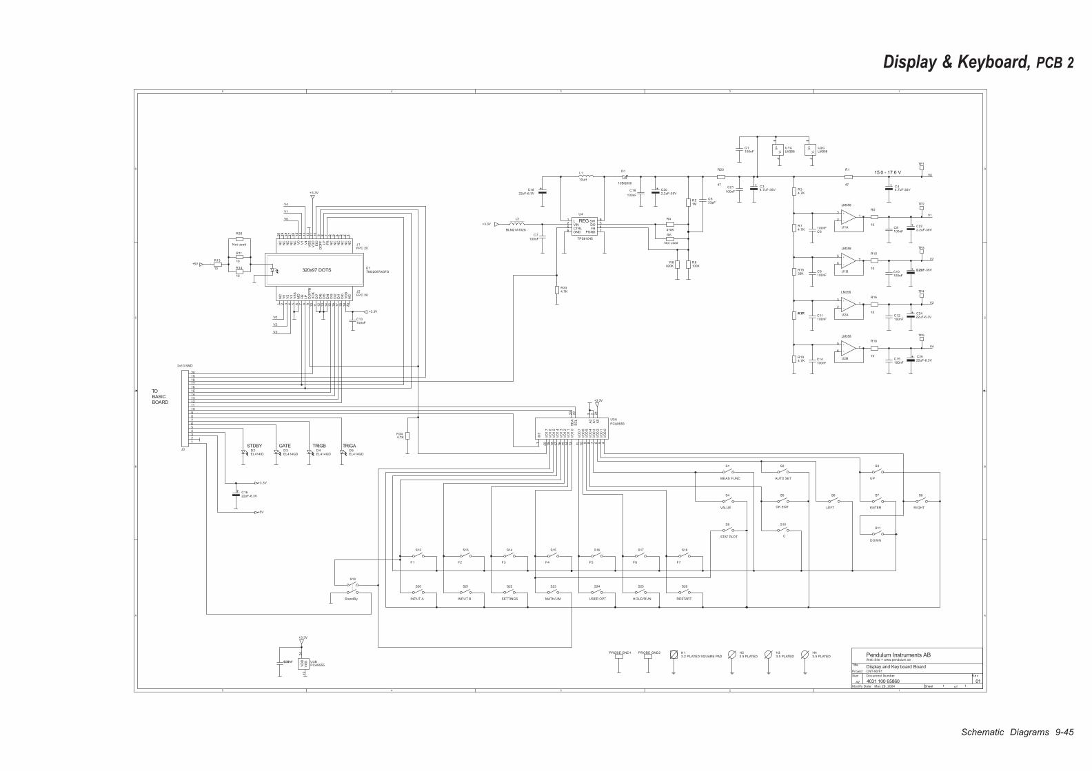
Display & Keyboard, PCB 2
Schematic Diagrams 9-45
5
5
4
4
3
3
2
2
1
1
D D
C C
B B
A A
V0
V0
V1
V4
V0
V2
V3
V3
V2
V1
V4
+3.3V
+5V
+3.3V
+3.3V
+3.3V
+3.3V
+5V
+3.3V
Title
Size Document Number Rev
Modify Date: Sheet o f
Project
01
Display and Keyboard Board
Pendulum Instruments AB
A2
1 1
4031 100 65860May 28, 2004
CNT-90/91
Web Site = www.pendulum.se
15.0 - 17.6 V
STDBY GATE TRIGATRIGB
TO
BASIC
BOARD
L1
10uH
S24
USER OPT
C11100nF
R18
10
H13.2 PLATED SQUARE PAD
S20
INPUT A
C7
100nF
C15100nF
S3
UP
C1622uF-6.3V
R1
47
U1CLM358
V+
8
V-
4
S18
F7
+
-
U2A
LM358
2
31
C533pF
S10
C
S14
F3
D3EL414GD
J1FPC 20
NC
1N
C2
NC
3N
C4
NC
5N
C6
FR
7LP
8D
OF
F9
EIO
10
VD
D11
VS
S12
V4
13
V1
14
V0
15
NC
16
NC
17
NC
18
NC
19
NC
20
S25
HOLD/RUN
L2
BLM21A102S
U3BPCA9555V
DD
24
VS
S12
S21
INPUT B
C9100nF
H23.5 PLATED
R5
10
R13
10
C13100nF
S8
RIGHT
C222.2uF-35V
S19
StandBy
C8100nF
C1100nF
U2CLM358
V+
8
V-
4
S1
MEAS FUNC
R334.7K
R174.7K
S6
LEFT
C202.2uF-35V
S15
F4
D4EL414GD
TP3
R20
47
C1822uF-6.3V
PROBE GND1
U3A
PCA9555
A0
21
A1
2A
23
SC
L22
SD
A23
I/O
0.0
4I/O
0.1
5I/O
0.2
6I/O
0.3
7I/O
0.4
8I/O
0.5
9I/O
0.6
10
I/O
0.7
11
I/O
1.0
13
I/O
1.1
14
I/O
1.2
15
I/O
1.3
16
I/O
1.4
17
I/O
1.5
18
I/O
1.6
19
I/O
1.7
20
INT
1
R35
Not used
S26
RESTART
1MR2
H33.5 PLATED
S22
SETTINGS
470K
R4
320x97 DOTSE1TM32097AGFG
+
-
U1B
LM358
6
57
C6100nF
R10
10
C2522uF-6.3V
820KR8
S13
F2
TP2
C19
100nF
C10100nF
PROBE GND2
S2
AUTO SET
C44.7uF-35V
R194.7K
S11
DOWN
REG
U4
TPS61045
L1
VIN2
CTRL5
GND6
SW8
DO3
FB4
PGND7
S16
F5
D5EL414GD
R14
10
H43.5 PLATED
R34.7K
S4
VALUE
R6
Not used
S23
MATH/LIM
+
-
U1A
LM358
2
31
C14100nF
C34.7uF-35V
R16
10
TP4J2FPC 20
NC
1
V0
2
V2
3
V3
4
VS
S5
MD
6
FR
7
LP
8
DO
FF
B9
XC
K10
DI7
11
DI6
12
DI5
13
DI4
14
DI3
15
DI2
16
DI1
17
DI0
18
VD
D19
NC
20
S12
F1
+
-
U2B
LM358
6
57
C12100nF
100KR9
S7
ENTER
C21
100nF
D2EL414ID
C17100nF
S9
STAT PLOT
S17
F6
R344.7K
TP5
S5
OK EXIT
R74.7K
C232.2uF-35V
C2422uF-6.3V
10BQ030
D1
J3
2x10 SMD
1234567891011121314151617181920
R11
10
R1533K
TP1

9-46 Schematic Diagrams
This page is intentionally left blank.

Chapter 10
Appendix
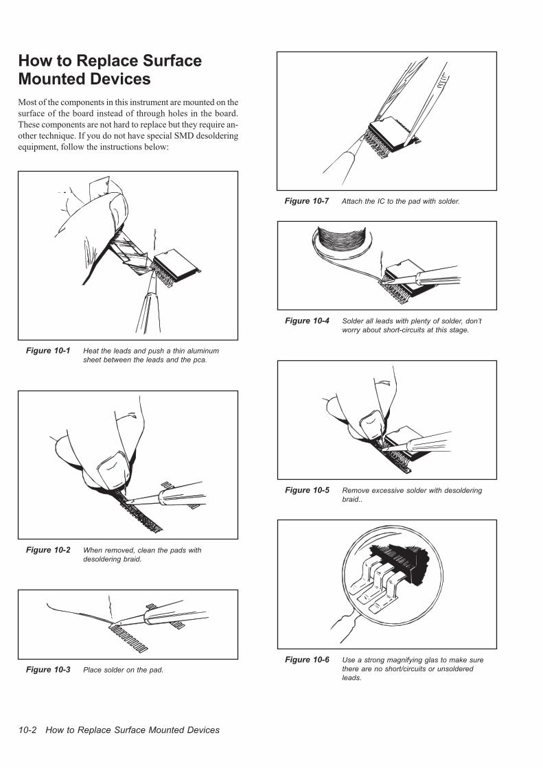
How to Replace SurfaceMounted Devices
Most of the components in this instrument are mounted on the
surface of the board instead of through holes in the board.
These components are not hard to replace but they require an-
other technique. If you do not have special SMD desoldering
equipment, follow the instructions below:
10-2 How to Replace Surface Mounted Devices
Figure 10-1 Heat the leads and push a thin aluminum
sheet between the leads and the pca.
Figure 10-2 When removed, clean the pads with
desoldering braid.
Figure 10-3 Place solder on the pad.
Figure 10-4 Solder all leads with plenty of solder, don’t
worry about short-circuits at this stage.
Figure 10-5 Remove excessive solder with desoldering
braid..
Figure 10-6 Use a strong magnifying glas to make sure
there are no short/circuits or unsoldered
leads.
Figure 10-7 Attach the IC to the pad with solder.
Electrostatic Discharge
Almost all modern components have extremely thin conduc-
tors and metal oxide layers. If these layers are exposed to elec-
trostatic discharge they will break down or perhaps even
worse, be damaged in a way that inevitably will cause a break-
down later on. The Electro-Static Discharge sensitivity of
MOS and CMOS semiconductors have been known quite a
while, but nowadays bipolar semiconductors and even preci-
sion resistors are ESD sensitive. Consider therefore all com-
ponents, pc-boards and sub-assemblies as sensitive to electro-
static discharge. The text below explains how you can mini-
mize the risk of damage or destroying these devices by being
aware of the problems, and learning how to handle these com-
ponents.
ESD sensitive options are packed in conductive containers
marked with this symbol.
• Never open the container unless you are at an ESD pro-
tected work station.
• Use a wrist strap grounded via a high resistance.
• Use a grounded work mat on your workbench.
• Never let your clothes come in contact with ESD sensitive
equipment even when you are wearing a grounded wrist
strap.
• Never touch the component leads.
• Never touch open connectors.
• Use ESD-safe packing materials.
• Use the packing material only once.
• Keep paper and nonconductive plastics etc. away from your
workbench. These may block the discharge path to ground.
Glossary
C
Calibration Ad-
justments
How to restore an instrument to perform in
agreement with its specifications.
CSA Canadian Standards Association
E
EN 61010-1 International safety standard
F
FLASH PROM Electrically erasable and reprogrammable
non-volatile semiconductor memory.
FPGA Field Programmable Gate Array
G
GPIB General Purpose Instrumentation Bus used for
interconnecting several measuring instruments
to a common controller.
I
I2C-bus An internal address and data bus for communi-
cation between microcontroller, measuring logic,
and options.
IEC International Electrical Commission
L
LCD Liquid Crystal Display
O
OCXO Oven-Controlled X-tal Oscillator
P
PCA Printed Circuit Assembly
PCB Printed Circuit Board
Performance
Check
A procedure to check that the instrument is
functionally operational and performs to its
specification. Must not require opening of cabi-
net. If the instrument passes the check it is con-
sidered calibrated.
PLL Phase-Locked Loop
Prescaler RF frequency divider
PWM Pulse Width Modulation
U
UCXO Un-Compensated X-tal Oscillator
USB The Universal Serial Bus is a simpler alternative
to GPIB.
Electrostatic Discharge 10-3
This page is intentionally left blank.
10-4 Glossary

Chapter 11
Index
11-2 Index
Index
AAdjustments
Timebase . . . . . . . . . . . . . . . . 7-3,7-4
CCalibration . . . . . . . . . . . . . . . . . . . . 7-2
Closed Case. . . . . 4-7,4-15,6-12,6-40
Command Reference . . . . . . . . . . 7-6
General Principles . . . . . . . . . . . . 7-2
Preventive Maintenance . . . . . . . . 5-2
Procedure
Timebase . . . . . . . . . . . . . . . . . 7-4
Voltage . . . . . . . . . . . . . . . . . . . 7-5
Test Equipment. . . . . . . . . . . . . . . 2-2
Caution Statements . . . . . . . . . . . . . 1-2
Circuit Symbols . . . . . . . . . . . . . . . . 9-2
CMOS
Logic Levels . . . . . . . . . . . . . 6-4,6-32
Communication Interfaces . . . . 4-9,4-17
Component Numbers. . . . . . . . . . . . 9-2
Crystal Oscillators
Adjustment . . . . . . . . . . . . . . . . . 7-14
Calibration . . . . . . . . . . . . . . . . . . 7-3
DDefault Settings . . . . . . . . . . . . . . . . 2-3
Display
Description . . . . . . . . . . . . . . 4-6,4-14
EElectrostatic Discharge
SEE ESD
EMI Filter
Location of . . . . . . . . . . . . . . 4-9,4-17
ESD . . . . . . . . . . . . . . . . . . . . . . . . 10-3
Ext. Arming Input
Performance Check . . . . . . . . . . . 2-6
Ext. Ref. Input
Description . . . . . . . . . . . . . . 4-8,4-16
Performance Check . . . . . . . . . . . 2-6
External Arming
Input Location. . . . . . . . . . . . 4-9,4-17
External Reference
Adjustment . . . . . . . . . . . . . . . . . 7-13
Input Location. . . . . . . . . . . . 4-9,4-17
FFan
Replacing . . . . . . . . . . . . . . . . 3-3,5-3
Fan Control
Description . . . . . . . . . . . . . . 6-7,6-35
Firmware Upgrade
Instructions . . . . . . . . . . . . . . . . . . 5-2
Frequency Range
Performance Check . . . . . . . . . . . 2-4
Front Panel
LCD Drivers . . . . . . . . . . . . . 4-6,4-14
GGPIB Communication
Location of Connector. . . . . . 4-9,4-17
Grounding . . . . . . . . . . . . . . . . . . . . 1-2
HHold-Off Function
Performance Check . . . . . . . . . . . 2-7
IImportant Information. . . . . . . . . 5-3,5-4
Input Amplifiers
AC/DC Coupling . . . . . . . . . . 4-6,4-14
Adjustment . . . . . . . . . . . . . . . . . 7-12
Attenuator. . . . . . . . . . . . . . . 4-6,4-14
Buffer . . . . . . . . . . . . . . . . . . 4-6,4-14
Comparator . . . . . . . . . . . . . 4-7,4-15
Crossover Switch . . . . . . . . . 4-7,4-15
Filter . . . . . . . . . . . . . . . . . . . 4-6,4-14
General Description . . . . . . . 4-6,4-14
Impedance Converter . . . . . . 4-6,4-14
Impedance Selector . . . . . . . 4-6,4-14
Limiter . . . . . . . . . . . . . . . . . 4-6,4-14
Logic Level Conversion . . . . 4-7,4-15
Trigger Level Generation . . . 4-7,4-15
Troubleshooting . . . . . . . . . . 6-8,6-36
Int. Ref. Output
Description . . . . . . . . . . . . . . 4-8,4-16
Performance Check . . . . . . . . . . . 2-6
Internal Reference Output
Location of . . . . . . . . . . . . . 4-10,4-18
Internal Reset
Processor Circuits . . . . . . . . 4-8,4-16
KKeyboard
Description . . . . . . . . . . . . . . 4-6,4-14
Performance Check . . . . . . . . . . . 2-2
LLine Voltage . . . . . . . . . . . . . . . . . . . 1-4
MMeasuring Functions
Performance Check . . . . . . . . . . . 2-6
Measuring Logic
Description . . . . . . . . . . . . . . 4-8,4-16
FPGA . . . . . . . . . . . . . . . . . . 4-8,4-16
Interpolators . . . . . . . . . . . . . 4-8,4-16
Troubleshooting . . . . . . . . . . . . . 6-55
Microprocessor & Memories
Troubleshooting . . . . . . . . . . . . . 6-43
Microprocessor Bus & Interfaces
Troubleshooting . . . . . . . . . . . . . 6-49
NNegative ECL
Logic Levels . . . . . . . . . . . . . 6-4,6-32
OOperating Conditions . . . . . . . . 6-4,6-32
Operation. . . . . . . . . . . . . . . . . . . . . 1-2
Options
Location of . . . . . . . . . . . . . . . . . . 3-2
Oscillator Circuits
Description . . . . . . . . . . . . . . 4-7,4-15
Oscillators
Calibration . . . . . . . . . . . . . . . 7-3,7-4
Oven Oscillator
Troubleshooting . . . . . . . . . . . . . 6-40
PPerformance Check
Frequency Range . . . . . . . . . . . . . 2-4
Front Panel Controls. . . . . . . . 2-2,2-3
General Information . . . . . . . . . . . 2-2
Hold Off Function . . . . . . . . . . . . . 2-7
Input Controls . . . . . . . . . . . . . . . . 2-5
Measuring Functions . . . . . . . . . . 2-6
Rear Inputs/Outputs . . . . . . . . . . . 2-6
Reference Oscillators . . . . . . . . . . 2-5
Resolution . . . . . . . . . . . . . . . . . . 2-5
RF Options . . . . . . . . . . . . . . . 2-7,2-8
Sensitivity . . . . . . . . . . . . . . . . . . . 2-4
Test Equipment. . . . . . . . . . . . . . . 2-2
Trigger Indicators . . . . . . . . . . . . . 2-4
Voltage . . . . . . . . . . . . . . . . . . . . . 2-4
Positive ECL
Logic Levels . . . . . . . . . . . . . 6-4,6-32
Power Supply
Description . . . . . . . . . . . . . . 4-8,4-16
Troubleshooting . . . . . . . . . . . . . 6-32
Power Supply Inlet
Location of . . . . . . . . . . . . . . 4-9,4-17
Power-On Tests . . . . . . . . . . . 4-10,4-18
Prescaler
Adjustment . . . . . . . . . . . . . . . . . 7-14
RF Option. . . . . . . . . . . . . . 4-10,4-18
Troubleshooting . . . . . . . . . . . . . 6-43
Primary Circuits
Repair. . . . . . . . . . . . . . . . . . 6-4,6-32
Index 11-3
Processor Circuits
Description . . . . . . . . . . . . . . 4-8,4-16
Protective Ground
Checking the Connection . . . . . . 6-59
RRear Inputs/Outputs
Performance Check . . . . . . . . . . . 2-6
Reference Oscillators
Performance Check . . . . . . . . . . . 2-5
Reinstalling the Cover . . . . . . . . . . . 3-3
Removing the Cover . . . . . . . . . . . . 3-2
Required Test Equipment
Checkup/Adjustment/Repair . . . . . 2-2
Resolution
Performance Check . . . . . . . . . . . 2-5
RF Input
Performance Check . . . . . . . . . . . 2-7
Replacing . . . . . . . . . . . . . . . . . . . 3-3
RF Options
Performance Check . . . . . . . . 2-7,2-8
SSafety Components . . . . . . . . . . . . 6-59
Safety Inspection . . . . . . . . . . 6-59,6-60
Sensitivity
Performance Check . . . . . . . . . . . 2-4
Signals. . . . . . . . . . . . . . . . . . . . . . . 9-2
Special Parts . . . . . . . . . . . . . . . . . . 8-2
Standard Parts . . . . . . . . . . . . . . . . . 8-2
Surface Mounted Devices . . . . . . . 10-2
TTest After Repair . . . . . . . . . . 6-59,6-60
Test Routines
Built-in . . . . . . . . . . . . . . . . 4-10,4-18
Tests
Internal Self-Tests. . . . . . . . . . . . . 2-2
Keyboard . . . . . . . . . . . . . . . . . . . 2-2
Short Form Specification. . . . . 2-4,2-5
Timebase
Calibration . . . . . . . . . . . . . . . . . . 7-3
Timebase Reference
Standard Oscillator . . . . . . . . . . . 6-12
Timebase Reference Circuits
Troubleshooting . . . . . . . . . . . . . 6-40
Trigger Indicators
Performance Check . . . . . . . . . . . 2-4
Troubleshooting
100 MHz Multiplier . . . . . . . 6-13,6-41
External Reference Circuits 6-13,6-41
Input Amplifiers. . . . . . . . . . . 6-8,6-36
Measuring Logic . . . . . . . . . . . . . 6-55
Microprocessor & Memories . . . . 6-43
Microprocessor Bus & Interfaces 6-49
Oven Oscillator . . . . . . . . . . 6-12,6-40
Power Supply . . . . . . . . . . . . . . . 6-32
Prescaler . . . . . . . . . . . . . . . . . . 6-43
Timebase Reference Circuits. . . . . . .6-12,6-40
TTL
Logic Levels . . . . . . . . . . . . . 6-4,6-32
UUtility Program . . . . . . . . . . . . . . . . . 5-3
VVoltage
Performance Check . . . . . . . . . . . 2-4
WWarning Statements. . . . . . . . . . . . . 1-2
Watchdog
SEE Internal Reset Circuit

This page is intentionally left blank.
11-4 Index