Embed Size (px)
Citation preview
COMPANY CONFIDENTIAL
293212 V1 280814
2nd December 2014
Plessey GaN-on-Silicon LED
The Impact of GaN-on-Silicon on SSL
www.plesseysemiconductors.com | COMPANY CONFIDENTIAL 2
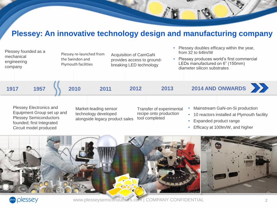
Plessey: An innovative technology design and manufacturing company
2014 AND ONWARDS
Acquisition of CamGaN
provides access to ground-
breaking LED technology
Market-leading sensor
technology developed
alongside legacy product sales
• Plessey doubles efficacy within the year, from 32 to 64lm/W
• Plessey produces world’s first commercial LEDs manufactured on 6” (150mm) diameter silicon substrates
Transfer of experimental recipe onto production tool completed
Plessey re-launched from the Swindon and Plymouth facilities
• Mainstream GaN-on-Si production
• 10 reactors installed at Plymouth facility
• Expanded product range
• Efficacy at 100lm/W, and higher
2013 2012 2011 2010
Plessey founded as a
mechanical
engineering
company
1917 1957
Plessey Electronics and
Equipment Group set up and
Plessey Semiconductors
founded; first Integrated
Circuit model produced

www.plesseysemiconductors.com | COMPANY CONFIDENTIAL 3
Plessey-owned land and buildings: ~53,000m2. operational plus an additional ~60,000 m2 of property for expansion
Manufacturing standards ISO9001, TS16949 (automotive), ISO14001, OHSAS 18001
Two wafer manufacturing lines
8-inch (200mm) wafer manufacturing facility: 1,550sqm, Class 1000, with better than Class 1 SMIF mini environment
6-inch (150mm) wafer manufacturing line: 1,200sqm, Class 10: GaN-on-Si for LED and power devices
Plessey’s LED Fab In Plymouth
COMPANY CONFIDENTIAL
293212 V1 280814
MaGIC — Manufactured on GaN-on-Si I/C
LED Technology TM
www.plesseysemiconductors.com | COMPANY CONFIDENTIAL 5
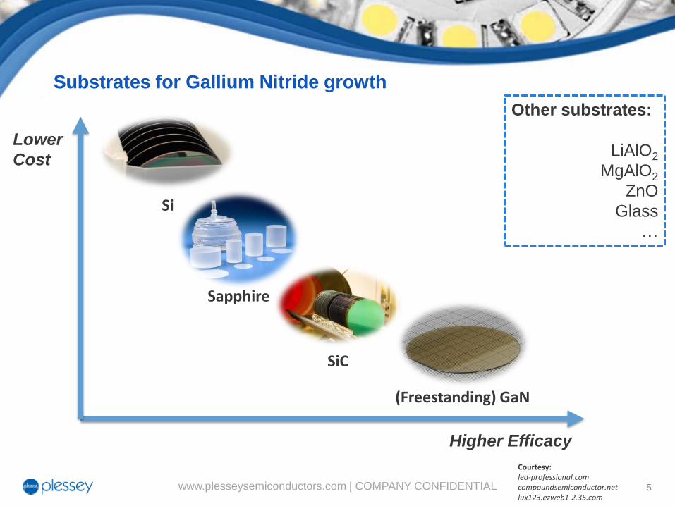
Substrates for Gallium Nitride growth
Other substrates:
LiAlO2
MgAlO2
ZnO
Glass
…
Courtesy: led-professional.com compoundsemiconductor.net lux123.ezweb1-2.35.com
Sapphire
SiC
(Freestanding) GaN
Si
Lower
Cost
Higher Efficacy
www.plesseysemiconductors.com | COMPANY CONFIDENTIAL 6
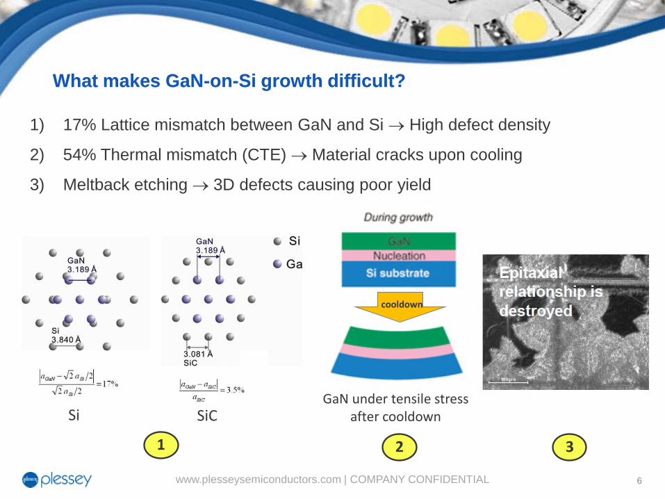
1) 17% Lattice mismatch between GaN and Si High defect density
2) 54% Thermal mismatch (CTE) Material cracks upon cooling
3) Meltback etching 3D defects causing poor yield
3
GaN under tensile stress after cooldown
2
cooldown
What makes GaN-on-Si growth difficult?
1
Si SiC
www.plesseysemiconductors.com | COMPANY CONFIDENTIAL 7 Courtesy: Rep. Prog. Phys. 76 (2013) 106501
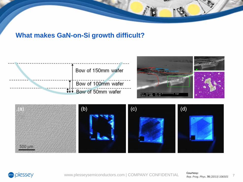
What makes GaN-on-Si growth difficult?
www.plesseysemiconductors.com | COMPANY CONFIDENTIAL 8
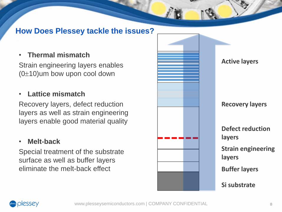
• Thermal mismatch
Strain engineering layers enables
(010)um bow upon cool down
• Lattice mismatch
Recovery layers, defect reduction
layers as well as strain engineering
layers enable good material quality
• Melt-back
Special treatment of the substrate
surface as well as buffer layers
eliminate the melt-back effect
How Does Plessey tackle the issues?
Si substrate
Strain engineering layers
Recovery layers
Active layers
Buffer layers
Defect reduction layers
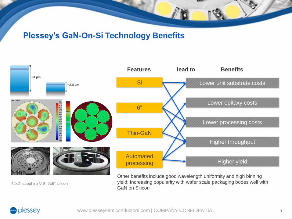
www.plesseysemiconductors.com | COMPANY CONFIDENTIAL 9
Si
6”
Thin-GaN
Automated
processing
Lower unit substrate costs
Lower epitaxy costs
Lower processing costs
Higher throughput
Higher yield
Benefits Features
Plessey’s GaN-On-Si Technology Benefits
42x2” sapphire V.S. 7x6” silicon
Other benefits include good wavelength uniformity and high binning
yield; Increasing popularity with wafer scale packaging bodes well with
GaN on Silicon
lead to
www.plesseysemiconductors.com | COMPANY CONFIDENTIAL 10
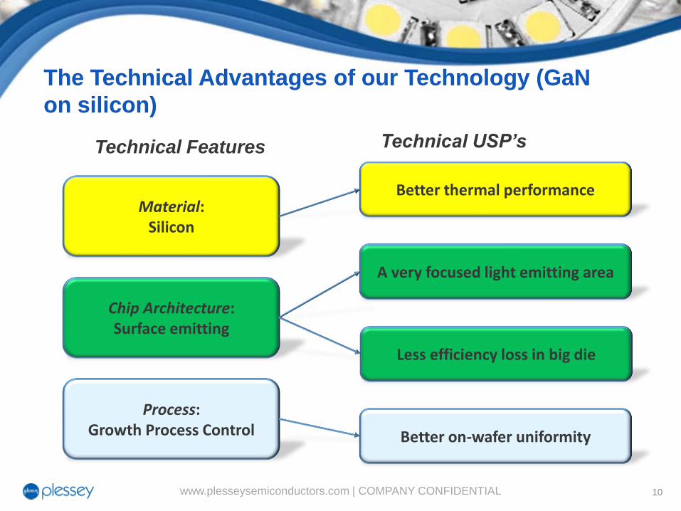
The Technical Advantages of our Technology (GaN
on silicon)
A very focused light emitting area
Technical Features Technical USP’s
Better thermal performance Material:
Silicon
Better on-wafer uniformity
Chip Architecture: Surface emitting
Process: Growth Process Control
Less efficiency loss in big die
www.plesseysemiconductors.com | COMPANY CONFIDENTIAL 11
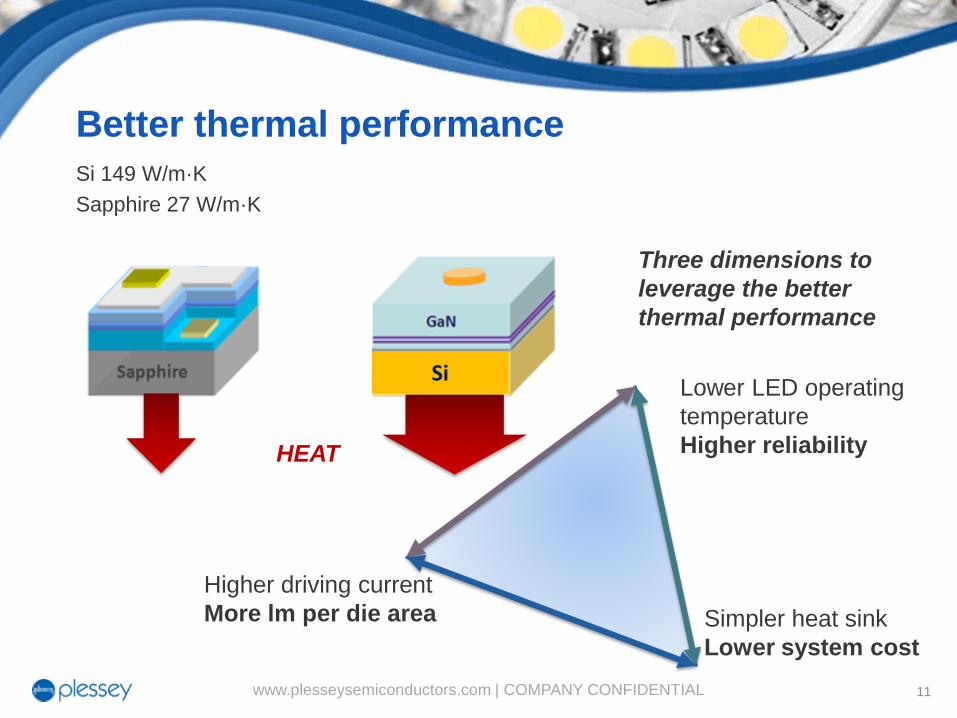
Si 149 W/m·K
Sapphire 27 W/m·K
Better thermal performance
Lower LED operating
temperature
Higher reliability
Higher driving current
More lm per die area Simpler heat sink
Lower system cost
Si
HEAT
Three dimensions to
leverage the better
thermal performance
www.plesseysemiconductors.com | COMPANY CONFIDENTIAL 12
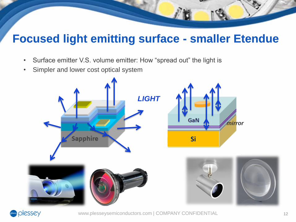
• Surface emitter V.S. volume emitter: How “spread out” the light is
• Simpler and lower cost optical system
Focused light emitting surface - smaller Etendue
Si
mirror
LIGHT
www.plesseysemiconductors.com | COMPANY CONFIDENTIAL 13
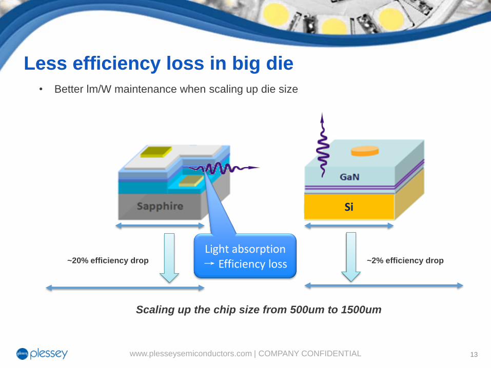
Less efficiency loss in big die
• Better lm/W maintenance when scaling up die size
Si
Light absorption → Efficiency loss ~20% efficiency drop ~2% efficiency drop
Scaling up the chip size from 500um to 1500um
www.plesseysemiconductors.com | COMPANY CONFIDENTIAL 14
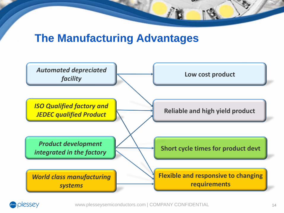
The Manufacturing Advantages
Reliable and high yield product
Low cost product Automated depreciated
facility
ISO Qualified factory and JEDEC qualified Product
Short cycle times for product devt Product development
integrated in the factory
World class manufacturing systems
Flexible and responsive to changing requirements
www.plesseysemiconductors.com | COMPANY CONFIDENTIAL 15
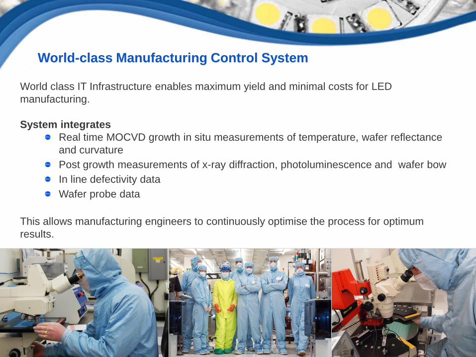
World class IT Infrastructure enables maximum yield and minimal costs for LED
manufacturing.
System integrates
Real time MOCVD growth in situ measurements of temperature, wafer reflectance
and curvature
Post growth measurements of x-ray diffraction, photoluminescence and wafer bow
In line defectivity data
Wafer probe data
This allows manufacturing engineers to continuously optimise the process for optimum
results.
World-class Manufacturing Control System
www.plesseysemiconductors.com | COMPANY CONFIDENTIAL 16
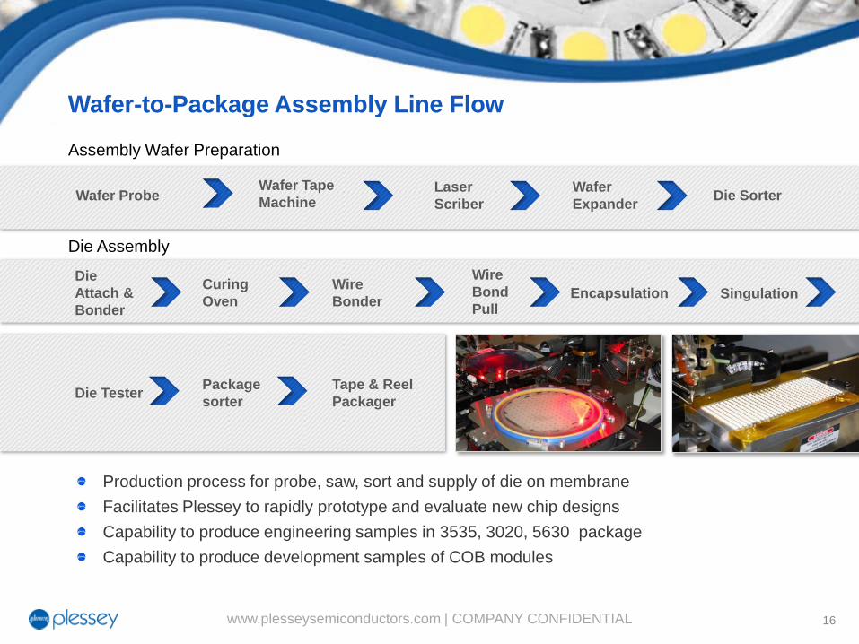
Wafer-to-Package Assembly Line Flow
Wafer Tape
Machine Laser
Scriber
Wafer
Expander Die Sorter
Die
Attach &
Bonder
Curing
Oven
Wire
Bonder Encapsulation
Die Tester
Die Assembly
Singulation
Package
sorter
Wire
Bond
Pull
Tape & Reel
Packager
Assembly Wafer Preparation
Production process for probe, saw, sort and supply of die on membrane
Facilitates Plessey to rapidly prototype and evaluate new chip designs
Capability to produce engineering samples in 3535, 3020, 5630 package
Capability to produce development samples of COB modules
Wafer Probe
COMPANY CONFIDENTIAL
293212 V1 280814
MaGICTM — Manufactured on GaN-On-Si I/C
Product Portfolio & Roadmap
18
To be added in the slide set but not published
Technology Roadmap
COMPANY CONFIDENTIAL
293212 V1 280814
MaGICTM – Manufactured on GaN-On-Silicon
Summary
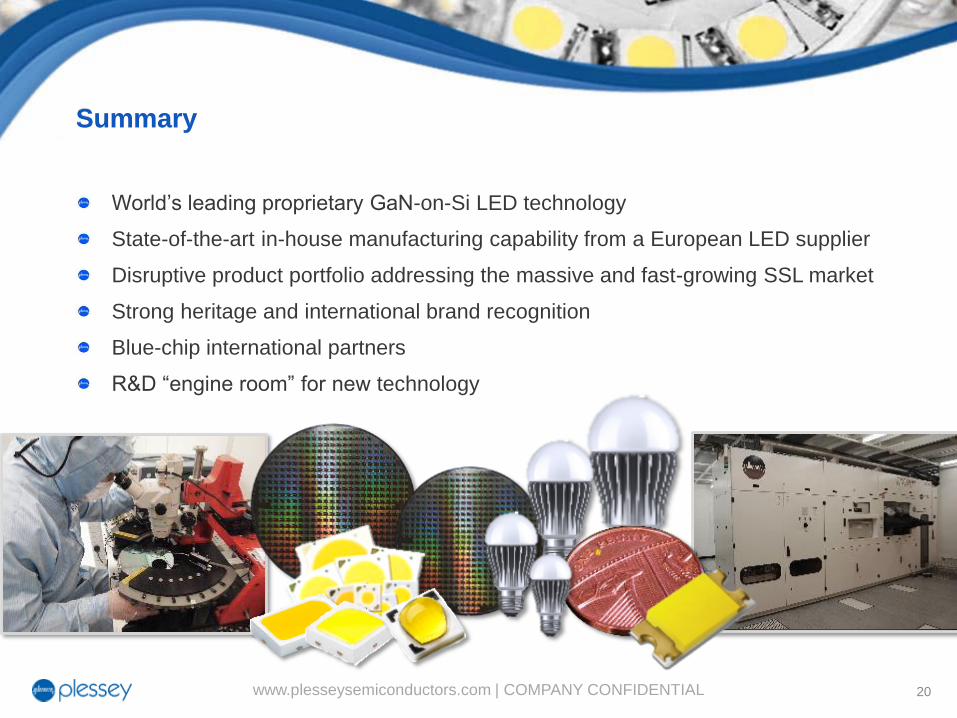
www.plesseysemiconductors.com | COMPANY CONFIDENTIAL 20
World’s leading proprietary GaN-on-Si LED technology
State-of-the-art in-house manufacturing capability from a European LED supplier
Disruptive product portfolio addressing the massive and fast-growing SSL market
Strong heritage and international brand recognition
Blue-chip international partners
R&D “engine room” for new technology
Summary