Embed Size (px)
Citation preview

1
REPORT DOCUMENTATION PAGE Form Approved
OMB No. 0704-0188 Public reporting burden for this collection of information is estimated to average 1 hour per response, including the time for reviewing instructions, searching existing data sources, gathering and maintaining the data needed, and completing and reviewing this collection of information. Send comments regarding this burden estimate or any other aspect of this collection of information, including suggestions for reducing this burden to Department of Defense, Washington Headquarters Services, Directorate for Information Operations and Reports (0704-0188), 1215 Jefferson Davis Highway, Suite 1204, Arlington, VA 22202-4302. Respondents should be aware that notwithstanding any other provision of law, no person shall be subject to any penalty for failing to comply with a collection of information if it does not display a currently valid OMB control number. PLEASE DO NOT RETURN YOUR FORM TO THE ABOVE ADDRESS.
1. REPORT DATE 27-09-2010
2. REPORT TYPE Final
3. DATES COVERED 9/1/2007 – 8/31/2010
4. TITLE AND SUBTITLE
5a. CONTRACT NUMBER FA9550-07-1-0053
Self-regenerating nanotips: Indestructable field-emission cathodes for low-power electric propulsion
5b. GRANT NUMBER
5c. PROGRAM ELEMENT NUMBER
6. AUTHOR(S)
5d. PROJECT NUMBER
Lyon B. King
5e. TASK NUMBER
5f. WORK UNIT NUMBER
7. PERFORMING ORGANIZATION NAME(S) AND ADDRESS(ES)
AND ADDRESS(ES)
8. PERFORMING ORGANIZATION REPORT
NUMBER Michigan Technological University
1400 Townsend Drive
Houghton, Michigan 49931
9. SPONSORING / MONITORING AGENCY NAME(S) AND ADDRESS(ES) 10. SPONSOR/MONITOR’S ACRONYM(S)
AFOSR 875 N. Randolph St. Arlington, VA 11. SPONSOR/MONITOR’S REPORT NUMBER(S) 12. DISTRIBUTION / AVAILABILITY STATEMENT
13. SUPPLEMENTARY NOTES
14. ABSTRACT
This research focuses on a field-emission cathode for use in Electric Propulsion (EP) that has the potential for very long lifetime due to its ability to be re-generated when the emitter tip becomes damaged. The field-emitting tips were formed by the application of an ion-extracting electric potential applied to a heated indium-coated tungsten needle, known as a liquid metal ion source (LMIS). The LMIS is then cooled, freezing in a solid nanotip at the apex. When the modified needle was then subjected to electron-extracting potentials stable and long-lived electron emission was observed. The focus of this investigation was to operate and quench a LMIS at ion emission currents from 2 to 25 µA to acquire micrographs of the surface morphology as a function of the ion emission current at quench. The LMISs were also tested against representative state-of-the-art field emitters that were made from tungsten.
15. SUBJECT TERMS
16. SECURITY CLASSIFICATION OF:
17. LIMITATION OF ABSTRACT
18. NUMBER OF PAGES
19a. NAME OF RESPONSIBLE PERSON
a. REPORT
b. ABSTRACT
c. THIS PAGE
30
19b. TELEPHONE NUMBER (include area
code) 906.487.2683
Standard Form 298 (Rev. 8-98)
Prescribed by ANSI Std. Z39.18
A
AFRL-OSR-VA-TR-2012-0446
2
Table of Contents
1. Experimental Equipment and Set-up............................................................................................ 3
1.1 Surface Morphology Research in the FE-SEM......................................................................... 3
1.2 Quenched Emitter Performance Analyses ................................................................................ 5
2. Experimental Procedures, Results, and Discussion ..................................................................... 6
2.1 Surface Morphology Research in the FE-SEM......................................................................... 6
2.2 Quenched Emitter Performance Analyses .............................................................................. 18
3. Conclusions .................................................................................................................................... 29
3.1 Surface Morphology Research in the FE-SEM....................................................................... 29
3.2 Quenched Emitter Performance Analyses .............................................................................. 30

3
Introduction A technique for re-generating solid-metal field-emitter tips using a liquid-metal ion source
(LMIS) has been extensively characterized.1-3 The LMIS was used to construct nano-scale metal structures intended for use as electron field-emission neutralizers for space applications. The feasibility of creating field emitting tips by quenching the ion emitting LMIS at emission currents ranging from 1 to 25 µA was demonstrated. It was shown that sharp nano-structures could be regenerated as long as there was a sufficient supply of indium to obtain ion emission. It was also found that the electron I-V characteristics of a field emitter could be altered by changing the ion emission current during the quench. The results of those experiments showed that as ion emission current during quenching was increased, the subsequent electron emission performance increased – inferring that the resulting solid emitter tip radii decreased. Applying the Fowler-Nordheim model to the electron I-V data yielded tip radii ranging from 230 to 80 nm at quench currents of 1 to 25 µA, respectively.2-4
The main goals of this research were twofold. The first goal of the research reported in this document was to examine the nanostructures formed during quench of an operational LMIS using electron microscopy and to understand how the morphology of these structures depends on the ion emission parameters during the generation process. The research focused on investigating the geometry of indium emitter tips that were formed by quenching an operating LMIS. Multiple tests were performed under a range of ion emission current conditions and then the tips were observed using a Field Emission Scanning Electron Microscope (FE-SEM) and the results were compared with Fowler-Nordheim models of data collected from the experiments. For each experiment the extraction electrode voltage was varied to investigate the emitter tip shape at ion emission currents ranging from 2 to 25µA.
The second goal of this study was to compare the performance of re-generable field emitters to that of solid tungsten emitters – chosen as a benchmark – under conditions comparable to those in the vicinity of an electric propulsion system operating on a spacecraft. For this study, a series of experiments were performed to observe the emission characteristics of each emitter for long durations of time in an ultra high vacuum (UHV) environment. Furthermore, each type of tungsten emitter and the re-generable emitters were tested while increasing the vacuum pressure from a UHV environment to > 10-5 Torr to determine how long and to what pressure emission could sustain. Each field emitter was exposed to elevated pressure conditions multiple times to determine their ability to tolerate cyclic damage.
1. Experimental Equipment and Set-up 1.1 Surface Morphology Research in the FE-SEM
The emitter fixture that was used for the FE-SEM experiments is shown in Figure 1. Modifications were made to the FE-SEM load-lock chamber that allowed a liquid metal ion source to be placed in the specimen chamber of the FE-SEM to perform emitter re-generation experiments in situ within the microscope. The custom fixture was equipped with electrical connections to operate the resistive heater and extraction electrode that are necessary to operate the LMIS. The electrical connections were made by three stainless steel discs that were connected to the heater and extraction electrode and were located underneath the top Teflon surface, shown in Figure 1. The three discs were used to mate with the internally mounted electrical interface. Implementing the custom fixture and

4
electrical connections allowed the dual ion/electron source to be operated in the specimen chamber of the FE-SEM.
Figure 1. Dual electron/ion source apparatus and the custom electrical interface mounted inside the Field Emission Scanning Electron Microscope.
The chamber was evacuated using a series of three ion pumps and vacuum pressure of 10-7 Torr
was maintained throughout testing. An electrical schematic of the completed re-generable emitter apparatus is shown in
Figure 2. For vacuum compatibility, the materials that were used to build the custom LMIS and support fixture included Teflon, stainless steel, and tungsten. Gap spacing between the emitter tip and the extraction electrode was ≤ 0.5 mm for all of the experiments.
Figure 2. Electrical schematic of the FE-SEM specimen fixture showing the heater supply, the extraction supply, and the ammeter placement.
Heater Supply
Extraction Supply
Extraction Electrode
Indium Coated Electrode
1.5”
Emitter Tip
Extraction Electrode
Internally Mounted Electrical Interface
Custom Specimen
Fixture
A
Extraction Electrode Interface

5
The internal electrical interface was installed permanently inside of the FE-SEM specimen
chamber. Electrical connections were made by inserting the custom specimen fixture so that the stainless steel electrodes that were connected to the heater and extraction electrode on the specimen fixture were made continuous with the internally mounted electrical interface by surface contact.
To achieve ion emission, the resistive emitter heater, shown previously in
Figure 2, was supplied with 2.75 A, 1.3 V with the purpose of maintaining the indium-coated electrode above the melting temperature of indium, which is 156.6°C. The extraction supply voltage was then increased until ion emission was established. For each set of experiments the extraction supply was increased until the desired ion emission current was reached and then the extraction electrode voltage was held constant while a pre-determined time was allowed to elapse, te. Leaving the extraction voltage constant, the heater power was turned off to quench the operating ion source. After the LMIS was allowed to cool for 30 seconds, the extraction supply was also turned off. Once the heater and extraction power supplies were off, the electron optics on the FE-SEM were engaged and micrographs of the emitter tip were acquired. After imaging the emitter tip, the electron optics were turned off and an electron I-V sweep was performed to apply to the Fowler-Nordheim model for tip radii estimations. The process of tip re-generation with subsequent imaging and electron I-V acquisition was repeated multiple times at a range of ion emission currents from 2 to 40 µA and a range of te from 10 to 240 seconds.
Between successive experiments the emitter tip surface morphology was ‘reset’ to eliminate any nano- or micro-structure on the surface. To ‘reset’ a smooth surface, the extraction power supply was current-limited at 100 µA while increasing the extraction voltage to about 7 kV. An emission current of 100 µA was sufficient to melt the sharp tips and the extraction voltage was high enough to cause arcing to destroy any locally sharp points on the apex.
1.2 Quenched Emitter Performance Analyses
The same fixture shown in Figure 2 that was used for the FE-SEM experiments was used for the set of comparison and elevated pressure experiments. As shown, a loop of tungsten wire was fixed to a Teflon block and the emitter tip was placed < 0.5 mm away from the extraction electrode. A micro-ammeter was placed in-line with the high voltage extraction electrode to measure the emission current. All of the components were constructed from Teflon, stainless steel, and tungsten.
All field emitters used in this study were formed by electrochemically etching tungsten wires to form a sharp tip. Two emitters, referred to as ‘bare’ tungsten emitters, were uncoated after etching and thus the current was emitted from the tungsten tip. The ‘re-generable’ emitters were created by first electrochemically etching tungsten needles in an identical process, however the etched needles were then coated in indium. Indium nanotips were formed at the emitter apex using a process described by Makela.5
Two bare tungsten emitters were tested. The first bare emitter tested was DC etched in a 2M NaOH solution to create a sharp and smooth emitter tip, as shown in Figure 3.6 The tungsten emitter was etched to have similar geometry to state-of-the-art Spindt-type field emitters. The second type of bare emitter that was tested was DC and then AC electrochemically etched in a 2M NaOH solution to create a roughened surface structure as shown in Figure 4.7 The roughened structure was intended to create an emitter with surface grooves, exactly the same as the field emitter that was coated with indium for the re-generable experiments. A possible indirect benefit of adding surface grooves was that the number of field-emitting nano-structures on the surface may have also increased.

6
Figure 3. DC electrochemically etched bare tungsten emitter.
Figure 4. DC and AC electrochemically etched bare tungsten emitter.
The comparison and elevated pressure experiments were performed in an ultra high vacuum chamber. The ultra high vacuum chamber is approximately 0.5 meters in diameter by 0.5 meters long. The chamber has a base pressure of 10-9 Torr, which is achieved by pumping with a single 280-L/s turbo-molecular pump that is backed by a 110-L/min dry scroll pump. The chamber is also equipped with a 300-L/s combination ion/sublimation pump that can maintain pressure of 10-9 Torr. An operating pressure of < 10-8 Torr was maintained throughout lifetime experiments.
2. Experimental Procedures, Results, and Discussion 2.1 Surface Morphology Research in the FE-SEM
Two sets of experiments were performed within the FE-SEM and are reported in Section 2.1.1 and 2.1.2. Section 2.1.1 describes the temporal evolution of a re-generable emitter tip. Section 2.1.2 is comprised of micrographs of quenched emitters and Fowler-Nordheim analyses from the quenched emitters at ion emission quench currents ranging from 2 to 20 µA. The data presented in Section 2.1.2
20 µm
30 µm

7
were then compared with data that were reported from similar experiments in an ultra high vacuum facility.2
2.1.1 Temporal Nano-structure Formation
It is well known that ions are emitted from a single jet-like protrusion when operating a liquid metal ion source.8,9 Therefore, prior to this investigation it was thought that a single jet-like protrusion would be solidified upon quenching an operating ion source. To investigate the surface morphology, the re-generable source was operated at ion emission currents of 10, 20, and 30 µA for 10-second intervals and imaged at each interval. The first experiment was performed at 10 µA of ion emission current, quenching the source every 10 seconds to show the evolution of the emitter tip after seven consecutive quenches at a constant ion emission current, as shown in Figure 5. For the 10-µA quenches, successive quenches created surface modification after about 40 seconds of ion emission.

8
Figure 5. FE-SEM micrographs of the emitter tip taken after consecutive quenches at ion emission current of approximately 10 µ A.
As shown in the micrograph, slight surface modification occurred after the first 10-second-
quench at 10 µA. After the next quench for 10 seconds the surface roughness appears to get more defined and not much changes between the second and third quench. After the fourth quench the emitter tip appears to have grown a Taylor cone structure. After the fifth quench of 10 seconds at 10 µA, the Taylor cone becomes more pronounced. After the sixth and seventh quenches, surface texture starts to become visible on the surface of the Taylor cone.
The same emitter was then reset and used to observe nano-structure formation at higher ion quenching currents. The experiment was performed by operating the re-generable source at an ion emission current of 20 µA with about 3 W of heater power for a quantity of seven 10-second intervals. After each time the emitter was quenched a micrograph was acquired, as shown in Figure 6. Just as with
10 µm 10 µm
10 µm 10 µm
10 µm 10 µm
10 µm 10 µm

9
the 10-µA experiment the images are intended to show the temporal evolution of the emitter tip after consecutive quenches at a constant ion emission current of 20 µA. After the first quench, at te = 10 s, a large cone formed at the center of the emitter apex. After 10 additional seconds of operation the cone appeared to retract and some nano-structures began to form. At an elapsed time of 30 s a very well structured Taylor cone formed with some nano-structure along the surface of the apex. Additional ion quenches didn’t generate many more nano-structure beyond the first 30 s.
Figure 6. FE-SEM micrographs of the emitter tip taken after consecutive quenches at ion emission current of approximately 20 µ A.
The micrographs show an interesting depression at the apex that resembles a “micro-volcano”
that formed after about 40 seconds of operation. It is possible the surface of the Taylor cone formed a
10 µm 10 µm
10 µm 10 µm
10 µm 10 µm
10 µm 10 µm

10
thin oxide layer, which could be responsible for holding the shape of the emitter between successive quenches. Indium tends to form indium oxide, In2O3, even when in a vacuum environment. Indium oxide melts at 1910°C so it could be possible that during subsequent quenches the emission current was sustained at the apex by liquid indium (Tmelt = 156.6 °C) beneath the oxide layer that was able to break through the layer, resulting in the “micro-volcano” structure due to depletion of indium. The emitter tip most certainly had to be at a greater temperature than the melting temperature of indium in order to sustain ion emission, which was the intent of heating the source with about 3 W during testing. Off-the-shelf LMISs used for Focused Ion Beams are similar to the emitters used for the testing reported here and typically use about the same amount of heater power. Whether indium or In2O3 the “micro-volcano” structure is not completely understood at this time.
After seven quenches, totaling 70 seconds of ion emission, the same re-generable source was again re-set. The re-generable source was operated at 30 µA of ion emission current and then quenched after 10 s of operation. The emitter tip was imaged and operated at 30 µA of ion emission current for six additional quenches at 10 second intervals, as shown in Figure 7.

11
Figure 7. FE-SEM micrographs of the emitter tip taken after consecutive quenches at ion emission current of approximately 30 µ A.
The apex of the emitter began to form a cone after the first 10-second-quench. The cone became
more defined after 20 seconds of operation and some nano-structure began to form along the tip’s surface. It wasn’t until after the third 10-second-quench that the nano-structure really started to become defined, as shown in the micrographs. Also, the “micro-volcano” structure appeared after the fourth quench, which was at the same point as in the 20-µA series when the structure formed.
To determine if the micrographs showed the evolution of the emitter tip or if the emitter tip relaxed after each time it was heated (between pictures in a given series of images) and formed a new structure during each 10-second emission iteration an experiment was performed to determine how much
10 µm
10 µm
10 µm
10 µm
10 µm 10 µm
10 µm 10 µm
12
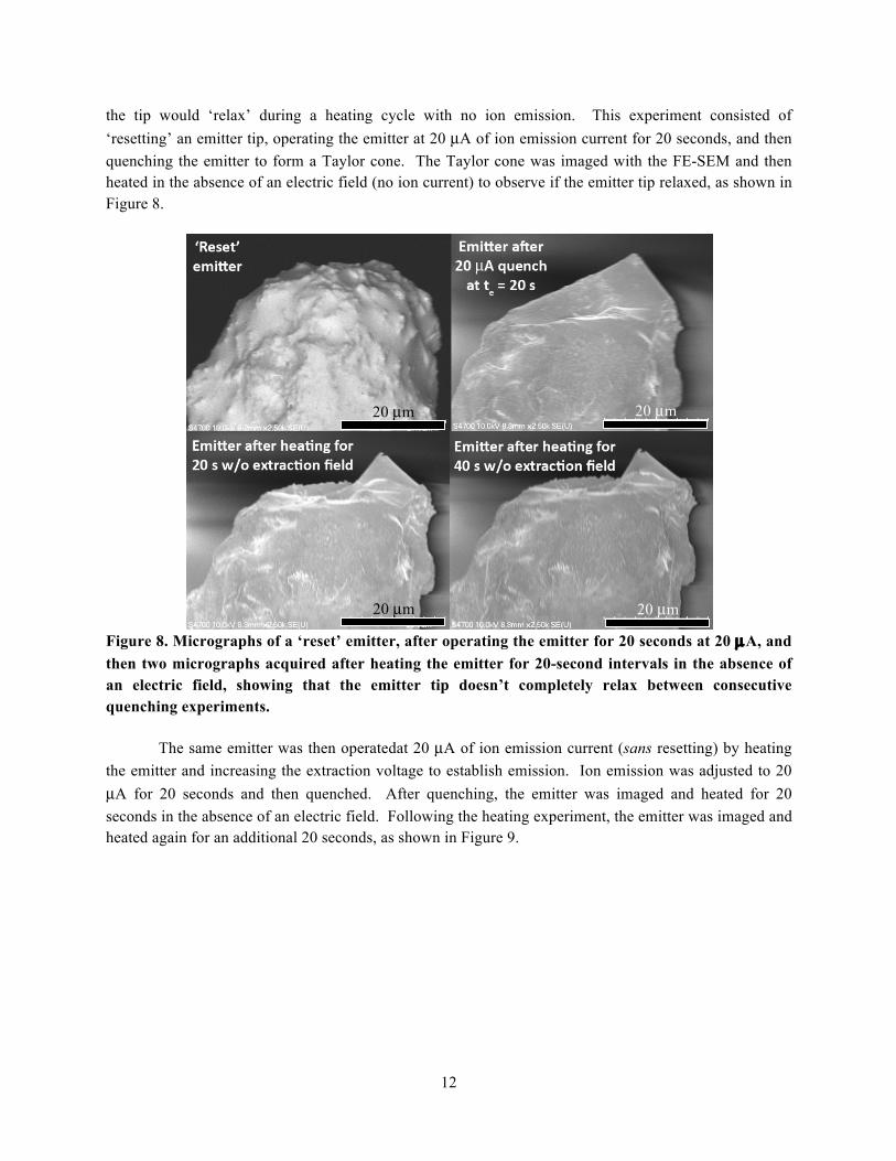
the tip would ‘relax’ during a heating cycle with no ion emission. This experiment consisted of ‘resetting’ an emitter tip, operating the emitter at 20 µA of ion emission current for 20 seconds, and then quenching the emitter to form a Taylor cone. The Taylor cone was imaged with the FE-SEM and then heated in the absence of an electric field (no ion current) to observe if the emitter tip relaxed, as shown in Figure 8.
Figure 8. Micrographs of a ‘reset’ emitter, after operating the emitter for 20 seconds at 20 µ A, and then two micrographs acquired after heating the emitter for 20-second intervals in the absence of an electric field, showing that the emitter tip doesn’t completely relax between consecutive quenching experiments. The same emitter was then operatedat 20 µA of ion emission current (sans resetting) by heating the emitter and increasing the extraction voltage to establish emission. Ion emission was adjusted to 20 µA for 20 seconds and then quenched. After quenching, the emitter was imaged and heated for 20 seconds in the absence of an electric field. Following the heating experiment, the emitter was imaged and heated again for an additional 20 seconds, as shown in Figure 9.
20 µm 20 µm
20 µm 20 µm

13
Figure 9. Micrographs of the same emitter shown in Figure 8 and then after operating the emitter for 20 seconds at 20 µ A, followed by two micrographs acquired after heating the emitter for 20 second intervals in the absence of an electric field, showing that the emitter tip doesn’t relax between consecutive quenching experiments.
It is impossible to say with certainty that the surface morphology remains the same between
subsequent thermal cycles but the micrographs show that the emitter tip surface doesn’t completely relax during each test. Since the emitter tip didn’t completely relax between successive tests, the images in Figure 5 through Figure 7 likely show the change in surface morphology as a result of the cumulative ion emission time.
2.1.2 Nano-structure Formation with Fowler-Nordheim Modeling
The purpose of this experiment was to use the FE-SEM to visually verify the trends that were observed via Fowler-Nordheim modeling of data taken in an earlier study within a UHV chamber2 In these earlier tests, the UHV chamber was equipped with an optical microscope that only had 90X magnification, which wasn’t high enough magnification to resolve the nano- and micro-structure of quenched emitters. Obtaining higher resolution micrographs motivated this series of experiments.
The re-generable emitters were quenched at multiple ion emission currents inside the FE-SEM. The FE-SEM was then used to image the nano-structure formation after quenching. Also, electron emission I-V sweeps were performed after each quench to estimate the emitter tip radii using the Fowler-Nordheim model. The emitter tip estimations were compared with the FE-SEM micrographs. The ion quenching currents that were chosen for the experiment ranged from 2 to 20 µA, operating each for 2 minutes exactly as done by Makela et al.2 After each quenched emitter was imaged and an electron I-V sweep was acquired the emitter tip was then ‘reset’ using the same procedure described previously of exposing the emitter tip to destructive electron emission conditions to smooth out and destroy surface features. The quenching experiments were performed in a randomized order but will be presented from
20 µm 20 µm
20 µm 20 µm

14
lowest-to-highest ion quenching current. The actual order of ion emission current before quenching was 20, 10, 5, 15, 20, 6, 16, 3, 10, and then 2 µA. After showing the individual results, a summary will be provided with all of the compiled data, including data from previous work in the UHV chamber.2
For each experiment the re-generable emitter was first exposed to electron ‘reset’ conditions. For the 1st reported experiment, the emitter was operated at 2 µA of ion emission current (at 3.3 kV) for 2 minutes and quenched. The image in Figure 10 shows a post-quench micrograph at 9000X, the highest resolution that was possible to obtain during testing. As shown, a cone-type structure formed with nano-scale features on the surface. Also, the volcano-type structure that was observed in the previous section was present in this test.
Figure 10. Micrograph showing a re-generable emitter tip after a 2 µ A quench for 2 minutes at magnification of 9000X.
After quenching and imaging the emitter tip, an electron I-V sweep was performed on the solidified emitter by increasing the extraction voltage up to 2.9 kV at 50 volt increments. A Fowler-Nordheim plot was created from the sweep data, as shown in Figure 11, with an R2 of 0.86 for the linear curve fit. Applying the Fowler-Nordheim model to the data resulted in an emitter tip radius estimate of 7.0 ± 1.4 nm.
Figure 11. Fowler-Nordheim plot from a re-generable emitter quenched after 2 minutes at 2 µ A, yielding a tip radius estimate of 7.0 ± 1.4 nm.
5 µm

15
After generating an emitter, imaging it, and acquiring Fowler-Nordheim data, the emitter was ‘reset’, re-generated, and the process was repeated. For each new experiment, the ion current at quench was adjusted to a value between 2 and 20 µA and then the quenched nano-structures were imaged using the FE-SEM and subjected to an electron I-V analysis. Table 1 shows the test conditions that were explored and includes the ion current before quench and the extraction voltage at quench. Table 1. Settings for tip re-generation experiments. The ion emission current and extraction voltage at quench are presented, as well as the chronological order that the data points were acquired and the extraction voltage required for about 1 µ A of electron emission current.
Ion Current at Quench
Extraction Voltage at Quench
Chronological Order of Data
(µA) (kV) 2 3.3 10 3 3.4 8 5 3.8 3 6 3.2 6
10 3.5 2 10 3.4 9 15 3.9 4 16 3.4 7 20 3.7 1 20 3.8 5
The FE-SEM micrographs from representative experiments are shown in Figure 12 and Figure
13. Each quenched emitter tip exhibited nano-structure formation on the surface. Many of the emitter tips also formed the “micro-volcano” structure. The complete set of micrographs are available in Makela.5
Figure 12. Micrograph showing the emitter tip nano-structure after a 10 µ A quench for 2 minutes.
5 µm

16
Figure 13. Micrograph showing the emitter tip nano-structure after a 20 µ A quench for 2 minutes.
As shown, the emitter tips are on a micro-scale with nano-scale features that formed on the
surface of the emitters. Although the exact size of the nano-features can’t be distinguished, electron I-V sweeps were acquired from each quenched emitter tip so that Fowler-Nordheim estimations could be made. All of the electron I-V data and the Fowler-Nordheim plots that were acquired in the FE-SEM are summarized in Table 1 and the data are plotted in Figure 14. Also reported in the table is the R2 value from each of the Fowler-Nordheim analyses. Included on the plot is the data taken in the UHV chamber.2 As shown, within the error bars there isn’t a discernable trend in the emitter tip radius as the ion current is varied.
Table 2. Emitter tip radius estimates from Fowler-Nordheim analyses of re-generated emitter tips at currents ranging from 2 to 20 µ A.
Ion Current
at Quench
Emitter Tip Radius Estimate
R2 value from F-N
Plot µA nm 2 7.0 ± 1.4 0.86 3 28.9 ± 5.8 0.96 5 22.6 ± 4.5 0.90 6 9.0 ± 1.8 0.91
10 5.5 ± 1.1 0.89 10 14.1 ± 2.8 0.79 15 29.6 ± 5.9 0.80 16 9.1 ± 1.8 0.88 20 27.3 ± 5.5 0.79 20 20.4 ± 4.1 0.77
5 µm

17
Figure 14. Data from experiments performed inside the FE-SEM and experiments performed in the UHV chamber that were reported by Makela, Washeleski, and King2 showing estimated emitter tip radii, using Fowler-Nordheim modeling, at ion currents before quenching of 1 to 25 µ A.
Looking at the FE-SEM micrographs shown previously, it was not possible to make accurate
emitter tip radii estimations visually. Unfortunately, the resolution of the micrographs was limited due to vibration in the fixture, since the LMIS was cantilevered off of a Teflon block. When the Fowler-Nordheim data that were acquired in the FE-SEM were combined with the data taken in the UHV chamber the plot in Figure 14 was generated. All of the data points that were obtained by Fowler-Nordheim modeling of electron I-V curves taken from quenched field emitters were in the same range. As shown, there is up to 25 nm of scatter in the data but all of the emitter tip radii estimations were between 5 and 50 nm.
Investigation of the surface structure of a quenched ion source using a Field Emission Scanning Electron Microscope resulted in the observation of a Taylor cone shaped structure, which was expected. However, each cone had multiple nano-structures that were solidified on the surface of the emitter tip. The micrographs revealed that the nano-structures were evenly spaced and approximately the same size all over the surface. Although electron emission was most likely occurring at the apex of the emitter due to the apex being in closest proximity to the extraction electrode, any of the nano-structures are capable of emission if the sharpest structures at the apex become incapable of emission.
The nano-structures were formed from quenching a liquid metal ion source at ion emission currents ranging from 2 to 30 µA. It was shown that a well-defined Taylor cone substructure forms after 20 to 30 seconds of ion emission and that the number of nano-structures that are formed on the surface of the Taylor cone tends to reach a maximum after 30 to 40 seconds of ion emission. The exceptions were two of the quenches, for unknown reasons a 5 and 15 µA quench didn’t produce a Taylor cone substructure or multiple nano-structures, however, they still had some sharp nano-structure. Another interesting observation was that the Taylor cones didn’t completely melt by adding heat in the absence of an electric field. While the temperature of the indium must have been sufficient to liquefy some of the

18
indium, since ion emission could be established and the bulk shape of the emitter could be deformed, it is possible that an indium oxide coating on the surface of the emitter could have been responsible for maintaining the shape of the emitter when heated without an applied electric field. As discussed in Section 2.1.1, indium oxide, In2O3, has a much higher melting temperature than indium so the oxide layer could have formed a solid ‘crust’ on the emitter surface. The Fowler-Nordheim model approximations reported in this paper had comparable tip radii estimations to those reported previously by Makela et al.2 Visually inspecting the nano-structures with the FE-SEM didn’t provide sufficient resolution to accurately determine the emitter tip radii, however, Fowler-Nordheim model radii estimations ranged from about 5 to 50 nm.
2.2 Quenched Emitter Performance Analyses
To establish electron emission from the bare tungsten emitters, the extraction electrode was biased positively with respect to the emitter (which was at ground potential) and the extraction voltage was increased until emission was acquired. The emission current was recorded using a micro-ammeter that was placed in-line with the extraction supply. For lifetime studies the extraction voltage was held constant and emission current was observed while at vacuum pressure < 10-8 Torr. For the elevated pressure experiments emission was first established at vacuum pressure < 10-8 Torr for 2 to 24 hours and then the ion pump was turned off to let the vacuum pressure slowly increase while observing the electron emission current. Once emission ceased the extraction voltage was decreased and the ion pump was turned back on to reduce the vacuum chamber pressure. When the vacuum pressure returned to < 10-8 Torr the same procedure was used to establish emission and expose the operating electron source to elevated vacuum pressure. The process was repeated until emission could no longer be achieved at reasonable extraction voltages. Ultimately, exposing the emitter tips to increased pressure multiple times would render the tip useless as an electron emitter.
For the re-generable emitter experiments, the same method discussed in Section 2.1 was used to re-generate the emitters. The procedure began with establishing ion emission by first heating the emitter, shown previously in
Figure 2, to 2.75 A, 1.3 V with the purpose of maintaining the indium-coated electrode above the melting temperature of indium, which is 156.6°C. The high-voltage extraction supply was then used to increase the potential between the emitter and the extraction electrode to obtain ion emission. For each set of experiments the extraction voltage was increased until the desired ion emission current was reached and then the extraction electrode voltage was held constant for one minute. Leaving the extraction electrode constant, the heater power was turned off to quench the operating LMIS. After the LMIS was allowed to cool for one minute, the extraction supply was also turned off – leaving sharpened nano-structures to use for electron emission. The re-generable emitters were then tested using the same procedure as the bare tungsten emitters.
2.2.1 Smooth Bare Tungsten Emitters
The first experiment was performed with a smooth bare tungsten field emitter, as shown previously in Figure 3. The emitter was electrochemically DC etched using the procedure described by Makela et al.2 The smooth bare tungsten emitter was tested in a UHV chamber at a vacuum pressure of 10-9 Torr. Prior to lifetime testing, an electron I-V curve was acquired by sweeping the extraction voltage

19
while recording the emission current so that the data could be used for Fowler-Nordheim analysis. The Fowler-Nordheim model was then used to estimate the emitter tip radius. For the smooth bare tungsten emitter, the model yielded a tip radius estimate of 13.9 ± 1.2 nm. Electron emission was then achieved by increasing the extraction electrode to 1.4 kV to obtain an emission current of 3 µA. The extraction voltage was then held constant and emission current was observed for 625 hours. To conclude the experiment, at te = 625 hours (chosen somewhat arbitrarily based on laboratory schedule constraints) the ion pump on the UHV chamber was turned off to increase the chamber pressure. At vacuum pressure of 10-7 Torr, and after less than two minutes, the emission ceased, as shown in Figure 15. A Fowler-Nordheim analysis was not performed after the 625 hour test because electron emission could not be acquired despite increasing the extraction voltage to 4 kV at UHV conditions.
Figure 15. Electron emission current from an electrochemically etched bare tungsten field emitter, showing a sudden decrease in emission current when background pressure was increased from 10-9 to 10-7 Torr. Emission current could not be established in subsequent testing (at an extraction voltage of 4 kV) indicating that the smooth bare tungsten emitter tip had been permanently damaged when exposed to an increased vacuum chamber pressure.
After the emission ceased, electron emission could not be re-established at 4 kV. The maximum
limit of 4 kV was arbitrarily chosen as an upper bound for the onset voltage for all of the experiments reported. Since emission couldn’t be established, the emitter tip must have been catastrophically damaged by the increase in vacuum pressure. Exposure to elevated pressure rendered the bare tungsten emitter useless as a field emission electron source. A second smooth bare tungsten field emitter was tested under similar conditions and was permanently damaged after two exposures to similar vacuum conditions.
2.2.2 Roughened Bare Tungsten Emitters
Two roughened bare tungsten emitters were tested for comparison. The roughened emitters were electrochemically DC and AC etched following the procedure described by Makela et al2 to create surface

20
grooves, as shown previously in Figure 4. Etching the surface grooves on the emitter was intended to make the electrode as close as possible to the indium-coated re-generable electrodes. An electron I-V sweep was acquired on the new roughened bare tungsten emitter at 10-8 Torr. Applying the Fowler-Nordheim model to the electron emission I-V sweep yielded a tip radius estimate of 4.6 ± 0.9 nm. After performing an electron I-V sweep, the extraction voltage was adjusted to establish electron emission.
The roughened bare tungsten emitter was then operated for about 20 hours to ensure the emission current was stabilized. Holding the extraction voltage constant, at te = 21.2 hours the vacuum chamber pressure was increased by turning off the ion pump. As the vacuum pressure increased the electron emission current was observed. Electron emission sustained for about 7 hours at background pressure ranging between 10-5 and 10-3 Torr, as shown in Figure 16, which was about 7 hours longer than emission sustained using smooth bare tungsten emitters. The background pressure was recorded until the ion gauge turned off due to an overpressure. Unfortunately, the vacuum chamber pressure couldn’t be recorded for the duration of some of the tests due to a lack in overlap of measuring range between the ion gauge and thermocouple gauge on the UHV system. Extrapolating the pressure data and analyzing data from other elevated pressure experiments, an approximate vacuum pressure of 5 x 10⁻⁵ Torr was estimated when emission ceased.
Figure 16. Electron emission current from a roughened bare tungsten emitter held at a constant extraction voltage of 2.8 kV from te = 3.1 hr to te = 28.9 hr as background pressure was increased for the first time. The region of unknown pressure was due to a lack of overlap in the cold cathode and thermocouple pressure gauges that were equipped on the vacuum facility.
Once emission ceased, the vacuum pressure was decreased to 10-9 Torr and another electron I-V
sweep was acquired. The electron I-V sweep taken prior to testing and after the first exposure to elevated pressure are both shown in Figure 17. The Fowler-Nordheim model was applied to the I-V sweep and yielded a tip radius estimate of 9.9 ± 2.0 nm, which was an increase in the emitter tip radius that was observed before exposing the operating field emitter to an increase in vacuum pressure.

21
Figure 17. Electron I-V sweep taken from a new roughened bare tungsten field emitter and an electron I-V sweep acquired after the first exposure of the emitter tip to elevated vacuum pressure. The Fowler-Nordheim model was applied to the I-V sweep after the first exposure and the tip radius was estimated at 9.9 ± 2.0 nm.
After the Fowler-Nordheim sweep was taken, electron emission was again established with the
roughened bare tungsten emitter at high vacuum. Emission was sustained at constant voltage for about 4 hours at a vacuum pressure of 10-9 Torr and then the vacuum pressure was increased while emission was observed. During the first 4.5 hours of the experiment, the emission current gradually decreased when vacuum pressure was constant in the 10-9 Torr regime, implying degradation of the tip. After 1.5 hours, emission ceased when vacuum pressure reached 2x10⁻⁵ Torr. Each exposure will be described in detail in the following paragraphs and the elevated pressure experiments and Fowler-Nordheim analyses will be summarized in Table 3.
During the second exposure to elevated pressure, emission from the roughened bare tungsten emitter lasted longer than electron emission from a smooth bare tungsten emitter. After emission ceased the vacuum pressure was decreased back to 10-9 Torr and an electron I-V sweep was performed to apply the Fowler-Nordheim model. The model yielded a tip radius estimate of 6.3 ± 1.3 nm, which was sharper than the estimated tip radius before exposing the emitter to increased pressure. A few possible reasons for a decrease in the tip radius after exposure to elevated pressure are discussed at the end of this section.
The roughened bare tungsten emitter tip was then used to achieve electron emission a third time at high vacuum. Emission was established at an extraction voltage of about 2.1 kV and the electron emission was then left to stabilize for about 4 hours. At te = 3.8 hours vacuum pressure was increased and the emission current was observed. The emission sustained until t=6.5 hours into the pressure range of 10-6 to 10-3 Torr. Extrapolating the pressure data, the pressure when emission ceased was approximately 6.3 x 10⁻⁶ Torr.
After emission ceased the vacuum chamber pressure was restored to 10-9 Torr and an electron I-V sweep was taken and the Fowler-Nordheim model was applied. The F-N model yielded a tip radius estimate of 4.6 ± 1 nm. Since numerous I-V sweeps were acquired and the Fowler-Nordheim model yielded emitter tips that were approximately the same size, it is possible that the roughened bare tungsten emitter may have multiple emission sites with similar nano-structures, as shown in the micrograph previously in Figure 4. Each time the roughened bare tungsten emitter was exposed to increased vacuum
22
pressure, it is possible that a single emission site was damaged but the next sharpest nano-structure could be used for subsequent testing.
For the fourth time, electron emission was established from the roughened bare tungsten emitter tip that had been exposed to increased pressure. Emission current was stable around 4 µA at constant voltage for about an hour and then the vacuum pressure was increased at te = 1 hr. Emission current sustained for about 5 hours at increased vacuum pressures ranging from 10-5 and 10-3 Torr. Extrapolating the pressure data, the vacuum chamber pressure when the emission failed was approximately 2 x 10⁻⁵ Torr.
Once emission ceased, an electron I-V sweep was acquired and the Fowler-Nordheim model was applied – yielding an emitter tip radius of about 7.1 ± 1.4 nm. Although the emitter tip radius estimations were within 10 nm of each other, the extraction voltage required to achieve electron emission after successive exposures to increased vacuum pressure had been increasing and decreasing randomly, indicating that the emitter tip was being damaged after some of the exposures and was getting sharper during other exposures to increased pressure which will be discussed later.
After the Fowler-Nordheim sweep, the extraction voltage was increased to 4 kV to obtain electron emission a fifth time. The initial emission current was 4 µA but quickly increased to about 6 µA. After staying constant at 6 µA for about two hours the vacuum pressure was increased. Emission sustained for about 20 hours at increased pressure. When emission ceased the vacuum pressure was decreased to 10-8 Torr and an electron I-V sweep was performed. The Fowler-Nordheim model was applied and resulted in an emitter tip radius of about 10.0 ± 2.0 nm. Thus far the roughened bare tungsten emitter tip was exposed to an increase in vacuum pressure five times and the estimated emitter tip radii have only varied by 5-6 nanometers.
After the tip estimate was calculated the extraction voltage was increased to 3.9 kV at high vacuum and the emission current was observed while exposing the roughened bare tungsten emitter to increased vacuum pressure for the sixth time. Emission lasted for about 4 hours as the pressure was increased. When emission ceased the vacuum pressure was returned to 10-8 Torr and another I-V sweep was performed, resulting in a Fowler-Nordheim emitter tip radius estimate of 7.8 ± 1.6 nm. Again, the emitter tip radius estimate was on the same order as the past couple of Fowler-Nordheim analyses.
After the Fowler-Nordheim analysis the same roughened bare tungsten emitter tip was exposed to increased vacuum pressure a seventh time. The emission current sustained for about 5 hours. Emission ceased at about 10-5 Torr. After emission ceased, the vacuum chamber pressure was decreased to 10-8 Torr and an electron I-V sweep was acquired. A post-test Fowler-Nordheim analysis yielded an emitter tip radius estimate of 14.0 ± 2.8 nm. After seven exposures to elevated vacuum pressure conditions, emission from the roughened bare tungsten emitter tip could not be established at an extraction voltage of 4 kV in high-vacuum conditions.

23
Table 3. Summary of data from the roughened bare tungsten field emitter exposure to elevated pressure. The field emitter survived 7 exposures to elevated pressure conditions before permanent failure.
Exposure Δt from UHV Fowler-Nordheim Approximate Vacuum Number to Failure Radius Estimate Pressure at Failure
hour nm Torr
Pre-test - 4.6 ± 0.9 -
1st 7 9.9 ± 2.0 5.0 x 10⁻⁵
2nd 1.5 6.3 ± 1.3 2.0 x 10⁻⁵
3rd 3.7 4.6 ± 1.0 6.3 x 10⁻⁶
4th 5 7.1 ± 1.4 2.0 x 10⁻⁵ 5th 20 10.0 ± 2.0 -
6th 4 7.8 ± 1.6 8.0 x 10⁻⁶
7th 5 14.0 ± 2.8 10-5 To summarize, the first roughened bare tungsten emitter that was tested survived 7 exposures to
elevated vacuum pressure within the test conditions of using a maximum extraction voltage of 4 kV to establish electron emission. Also, the first roughened bare tungsten emitter sustained between 1.5 and 20 hours of electron emission after the increase in pressure began for each experiment. A second roughened tungsten field emitter was fabricated and tested in an identical fashion; this emitter survived 4 exposures to elevated pressure and emission sustained from 1.4 to 20 hours while pressure was increased. The maximum pressure that was measured before emission ceased was 9.9 x 10⁻⁵ Torr. Both roughened emitters demonstrated longer lasting emission and survived more exposures to elevated pressure than the smooth bare tungsten emitters, as summarized at the end of Section 2.2.3 in Table 4.
2.2.3 Re-generable Field Emitters
To investigate the lifetime of re-generable emitters, a dual ion/electron source fabricated according to the technique described in Makela2 was placed in the UHV chamber and the vacuum chamber pressure was reduced to 10-9 Torr. The emitter was then heated and operated at 20 µA of ion emission current for one minute and then quenched to preserve a solid indium nanotip at the apex. The polarity of the extraction electrode was then reversed to achieve electron emission and the extraction electrode voltage was increased to obtain electron emission at 4 µA. The voltage required for 4µA of electron emission current was 4.1 kV; the extraction electrode was then voltage-limited at 4.1 kV for the remainder of the experiment. The re-generable field emitter was tested at 4 µA to subject the emitter to the same current as the tungsten field emitters.
Within the first hour of the lifetime test, the emission current increased to approximately 11 µA for a few minutes and then quickly decreased down to about 3 µA as shown in Figure 18. The emission current at constant voltage fluctuated between about 2 and 4 µA after the first hour until about te = 600 hours. At 600 hours into the experiment the emission quickly increased to about 5 µA and then slowly decreased down to about 3 µA again. At te = 950 hours of operation the experiment was voluntarily ceased for 5 hours to observe if the emission current would return to the same magnitude when turned back on. The experiment was paused by simply decreasing the extraction voltage from 4.1 kV to 0 kV.

24
Figure 18. Electron emission lifetime experiment from a single-needle re-generable emitter quenched at ion emission current of 20 µ A, showing locations of voluntary shutdowns. The extraction voltage was 4.1 kV and the vacuum pressure was ~10-9 Torr throughout the experiment.
The experiment was paused for 5 hours and then the extraction electrode was increased back to
the original setpoint of 4.1 kV. The emission current increased to almost 10 µA after the onset of emission but quickly decreased to about 5 µA at te = 952 hours. Then the electron emission current remained at 5 µA until approximately t = 975 hours and then rapidly decreased to 2 µA. Once reaching 2 µA the emission current slowly increased up near 3 µA until te = 1025 hours. The experiment was then voluntarily paused again for a span of 4 hours. During the 4 hour period of downtime, an electron I-V sweep was taken to estimate the emitter tip radius. Applying the Fowler-Nordheim model to the I-V data yielded a tip radius estimate of 9.5 ± 1.9 nm
After this second shutdown, the extraction voltage was increased back to the setpoint of 4.1 kV. As the extraction voltage was increased the electron emission current increased to 3 µA ± µA for 435 hours of operation, bringing the total duration of the lifetime test thus far to 1460 hours. At te = 1460 hours, the experiment was voluntarily interrupted again to obtain another electron emission I-V sweep. The I-V sweep was taken to determine if any change in tip radius was apparent from the first I-V sweep. The Fowler-Nordheim model was applied to the electron I-V data acquired during the third shutdown and yielded a tip radius estimate of 16.4 ± 3.3 nm.
Following the I-V sweep, the extraction voltage was again increased to 4.1 kV. The emission current gradually increased back to near 3 µA as the extraction voltage was increased. The lifetime experiment was continued for 300 additional hours, bringing the total lifetime test to about te = 1750 hours. The lifetime experiment was ended after 1750 hours due to the necessity to use the UHV chamber to perform other experiments. To end the lifetime experiment the extraction voltage was turned off and then a final electron emission I-V sweep was taken to estimate the nano-structure tip radius. The Fowler-Nordheim plot was applied to the electron I-V data from the fourth sweep and yielded a tip radius estimate of 16.2 ± 3.2 nm.
To compare with the single needle bare tungsten field emitters that were exposed to increased vacuum pressure, the same elevated vacuum pressure experiments were performed with the re-generable

25
emitters. The re-generable emitter was first operated as an ion source for 1 min at 20 µA, while heating the emitter with 2.25 A at 0.3 V. After 1 min the heater was turned off and the ion emission was quenched. The extraction voltage was then reversed to obtain electron emission and a Fowler-Nordheim analysis was performed on the ‘New’ emitter at 10-8 Torr, as shown in Figure 22. The Fowler-Nordheim model resulted in a tip estimate of about 13.7 ± 2.8 nm.
After the I-V sweep, the extraction voltage was increased to 3.8 kV to obtain electron emission. During the first 20 min of operation at 10-8 Torr the emission current had increased to about 25 µA so the extraction voltage was decreased to 2.1 kV in an attempt to keep the emission current around 4 µA. After the emission current remained relatively constant for approximately 1 hour the ion pump on the UHV chamber was turned off to increase the background pressure. The data that were recorded are shown in Figure 19, along with a bound of the possible background pressure. Extrapolating the pressure data, the vacuum chamber pressure was estimated at 8 x 10⁻⁵ Torr. As shown, electron emission from the quenched re-generable emitter sustained for over 15 hours.
Figure 19. Electron emission current from a quenched re-generable emitter held at a constant extraction voltage of 2.1 kV from te = 0.3 hr to te = 20 hr as background pressure was increased.
Once emission ceased, the ion pump on the vacuum facility was turned back on and vacuum
pressure was decreased to 10-8 Torr. An electron I-V sweep was performed on the emitter to obtain an estimate of the nano-structure radius that was emitting electrons, as shown in the ‘New + 1 Exposure’ data in Figure 22. The Fowler-Nordheim model resulted in a tip radius estimate of 12.8 ± 2.6 nm.
The extraction voltage was then increased to 6.1 kV to obtain an electron emission current of about 4 µA. The extraction voltage was adjusted during the first 30 minutes because the emission current kept increasing. At te = 30 minutes the extraction voltage was set to 3.4 kV to return the emission current to about ~5 µA. The extraction voltage was held at 3.4 kV for the remainder of the experiment, which was an increase of 1.3 kV in the extraction voltage that was necessary to obtain the same magnitude of emission current as before the emission ceased. Once the emission current remained stable for 2 hours,

26
the ion pump on the UHV system was turned off again to increase the background pressure. Electron emission current was maintained for nearly 50 hours after turning off the ion pump and increasing the vacuum pressure from 10-8 Torr to between 10-5 and 10-3 Torr, as shown in Figure 20.
Figure 20. Electron emission current from the same quenched re-generable emitter used in the test of Figure 19. The emitter was held at a constant extraction voltage of 3.4 kV from te = 0.5 hr to te = 50 hr as background pressure was increased.
After electron emission ceased, the ion pump on the UHV chamber was turned back on and the
chamber pressure was decreased back to 10-8 Torr. An electron I-V sweep was acquired, as shown by the ‘New + 2 Exposures’ data in Figure 22. The Fowler-Nordheim model was applied to the sweep and resulted in a tip radius estimate of about 15.5 ± 3.1 nm. The emitter tip after the first exposure was sharper than the emitter tip after the second exposure, which was expected.
After emission ceased, the vacuum pressure was restored to 10-8 Torr and electron emission couldn’t be achieved at an extraction voltage of up to 4 kV. The tip must have sustained damage from the two consecutive exposures to elevated background pressure, so the field-emitting nanostructures were re-generated through a sequence of heating, ion-emission, and quenching. The tip was operated at an ion emission current of 20 µA at 10-9 Torr for 1 min while supplying 2.25 A and 0.3 V of heater power. The emitter tip was then quenched and an electron I-V sweep was acquired, as shown by the ‘Re-generated’ data in Figure 22. The Fowler-Nordheim model was applied to the electron I-V sweep and resulted in a re-generated nano-structure radius of about 14.3 ± 2.9 nm, which was sharper than the emitter tip before re-generating it.
The freshly re-generated emitter tip was then operated as an electron source for over 150 hours at a background pressure of 10-9 Torr to demonstrate reliable operation from an emitter tip that had been exposed to increased background pressure multiple times and then had been re-generated, as shown in Figure 21. The extraction voltage was held at 4.1 kV from te = 0 to te = 1.5 hr and then the extraction voltage was decreased to 2.5 kV due to a rapid rise in emission current. The extraction voltage was held at 2.5 kV for the remainder of the experiment.

27
Figure 21. Extended duration experiment for an electron emitter that was re-generated by heating, acquiring ion emission, and then re-quenching after being damaged in the test sequences of Figure 19 to Figure 20. The extraction voltage was held constant at 2.5 kV from te = 1.5 hr to te = 175 hr and the test was ended by increasing the vacuum chamber pressure after over 150 hours of operation.
At te = 166 hr, the ion pump on the UHV chamber was turned off and the emission current was
observed as tank pressure increased. At te = 175 hr, the emission ceased. Once electron emission ceased, the ion pump on the UHV chamber was turned back on and vacuum pressure was decreased to 10-9 Torr. A final electron I-V sweep was performed, as shown by the ‘Re-generated + 1 Exposure’ data in Figure 22, resulting in a nano-structure radius estimation of 9.7 ± 1.9 nm after applying the Fowler-Nordheim model. Exposure to elevated pressure should have increased the emitter tip radius, however, emitter tip degradation didn’t occur in this case. Rarely, emitter tip performance increased after exposure to elevated pressure.

28
Figure 22. Fowler-Nordheim sweeps taken during each test sequence of operating a re-generable field emitter in UHV conditions and then exposing the emitter to an elevated vacuum pressure environment. After two exposures to elevated pressure conditions the emitter tip was re-generated.
The results from the comparison of the smooth bare tungsten, the roughened bare tungsten, and
the re-generable emitter are summarized in Table 4. The table includes the length of time that emission could sustain at elevated pressure, the number of times the emitter was exposed to an increased vacuum pressure before permanent failure was observed, and the magnitude of the maximum vacuum pressure that was recorded while emission sustained.
Table 4. Emitter tip comparison table displaying how long the emitter tips lasted at elevated pressure, how many exposures to increased pressure caused permanent failure, and the maximum vacuum chamber pressure that emission could sustain.
Emitter Type # of Tested Emitters
Emission Duration at Elevated Pressure
# of Exposures Before Failure
Maximum Tank Pressure Reached
Smooth Bare Tungsten 2 1 - 5 min 1 - 2 10-7 Torr Roughened Bare Tungsten 2 1.4 - 20 hr 4 - 7 10-5 Torr
Re-generable Emitter 2 6 - 45 hr Unlimited1 10-3 to 10-5 Torr The series of experiments performed with a re-generable emitter demonstrated longer-life
operation than single bare tungsten field emitters at increased vacuum pressures. While the quenched re-generable emitter required an increase in extraction electrode voltage after each exposure to increased vacuum pressure, the re-generable emitters survived more harsh conditions than bare tungsten emitters
1 where ‘Unlimited’ refers to the capability to re-generate the tip as long there is a sufficient metal supply available on the emitter tip.

29
and they appear to be more robust field emission electron sources. The smooth bare tungsten field emitters were irreversibly destroyed after only cycling them at increased vacuum pressures a couple of times, while the indium-coated emitters demonstrated the ability to be restored to their original performance by re-quenching them under ion-emitting conditions after being damaged.
Lifetime experiments demonstrated that the re-generable field emitters could sustain electron emission current for long periods of time and Fowler-Nordheim modeling of the emitter tip during voluntary shutdowns throughout the lifetime experiment yielded sharp emission sites on the order of 10’s of nm. The sharp nano-structures successfully demonstrated electron emission at an emission current of about 3 µA for 1,750 hours from a single-needle that was quenched at an ion emission current of 20 µA. Emission current from the re-generable emitters stayed relatively constant for the long duration tests while the current degraded over time for both types of bare tungsten emitters.
Some of the emitter tips that were exposed to elevated vacuum chamber pressure demonstrated better electron emission performance after exposure. One possible explanation for this is that electron emission could have occurred from multiple emission sites simultaneously. During some of the experiments in the UHV chamber, when an emitter was used to obtain over 10 µA of electron emission current, multiple locations on the emitter tips could be observed through the optical microscope that were glowing blue. It is possible that the local electric field enhancement was very similar at numerous locations, so any of the locations that sustained damage due to elevated pressure conditions could have easily been replaced by other sharp locations. Another possibility is that ion sputtering at higher vacuum pressure could have actually sputtered away a few of the atoms on the field-emitting nano-structures, temporarily leaving an even sharper emitter.
3. Conclusions 3.1 Surface Morphology Research in the FE-SEM
The main purpose of the FE-SEM experiments was to observe what happened to the surface morphology after quenching a liquid metal ion source and to compare the results with Fowler-Nordheim modeling. From literature, it was expected that a single jet-like protrusion would form at the tip of a Taylor cone. It was also expected that the geometry of the single protrusion would change depending on the ion emission current that was being emitted upon quenching. A Taylor cone structure did form, however a jet-like protrusion could not be detected from the micrographs. An interesting and un-anticipated observation from the micrographs revealed multiple nano-structures of similar geometry covering the apex of the emission electrode. As the quenching process was repeated, the protrusions that were formed became more and more defined and between subsequent quenches the overall structure of the Taylor cones maintained their shape, even when tested solely with heat in the absence of an electric field.
Formation of multiple protrusions from a quenched liquid metal ion source was a phenomenon that had never been observed but is very advantageous for re-generable cathodes. Since all of the nano-structures had very similar electric field enhancement, emission could have occurred from multiple nano-structures simultaneously. The multiple nano-structures that were formed on the re-generable field emitters could even act as a field emitting array, like Spindt-type arrays and carbon nanotube mesh.
Another interesting feature was also present in many of the micrographs that were taken after quenching an operating liquid metal ion source multiple times. A hollow depression that looked like a “micro-volcano” formed at the emitter tip apex after subsequent 10-second quenches and appeared to

30
form after the fourth 10-second quench in most cases. It is not clearly understood at this time but it is possible that a thin oxide layer is present on the surface of the emitter, causing the emitter tip to retain its shape during repeated quenching while the emission is sustained by depleting liquid indium from the apex.
3.2 Quenched Emitter Performance Analyses
In order to determine performance characteristics of re-generable and tungsten emitters, lifetime experiments were performed using three types of field emitters; smooth bare tungsten, roughened bare tungsten, and the re-generable emitters. Single-needle tungsten field emitters were used for comparison rather than Spindt-type emitters to avoid complicated micro-fabrication that is required to build Spindt devices. Since Spindt-type emitters are made up of thin films of refractory metals, such as molybdenum or tungsten, the pure tungsten emitters should have had similar performance.
The main purpose of the comparison experiments was to determine if re-generable field emitters had similar emission characteristics to bare tungsten emitters and to determine what, if any, advantages re-generable emitters had over bare tungsten emitters that were approximately the same physical size and geometry. The experiments with the electrochemically DC etched smooth bare tungsten emitters demonstrated the least reliable operation and were the most prone to permanent damage after the fewest exposures to elevated vacuum pressure environments. The smooth bare tungsten emitters ceased to function after 1-2 cycles from 10-8 to 10-7 Torr. In addition, emission would cease after only a few minutes at increased pressure.
The experiments that were performed with the electrochemically DC and AC etched roughened bare tungsten emitters exhibited better performance than the smooth bare tungsten emitters. When exposed to increased vacuum pressure, the roughened emitters could sustain emission for up to 22 hours at pressure up to 10-5 Torr. Also, the roughened emitters survived 4-7 exposures to increased pressure before the emitters were permanently damaged. As mentioned, the smooth bare tungsten emitters lasted a maximum of 2 exposures. The increased lifetime was most likely due to the multiple nano-scale sharp ridges that were created during the AC electrochemical etch. Where the DC etched emitters were smooth and had a single sharp nano-structure, the AC etched emitters had multiple longitudinal nano-structures that were capable of field emission, which allowed the roughened bare tungsten emitters to last longer than smooth bare tungsten. However, emission current from the roughened bare tungsten emitters decreased over the duration of most experiments in UHV conditions, much like the Spindt-type arrays and carbon nanotube emitters in literature, indicating emitter tip degradation over time.
The re-generable emitters demonstrated the longest lasting performance at elevated pressure of the three emitters – even before re-generation. The re-generable emitters survived up to 45 hours at vacuum pressures up between 10-3 to 10-5 Torr. While the re-generable emitters could only be exposed to elevated pressure two times before emission could no longer be achieved at up to 4 kV of extraction voltage, they could then be re-generated into a like-new condition and subsequently operated for 100’s of hours or longer. Therefore the re-generable emitters could potentially be cycled to increased pressure an almost unlimited number of times. Not only did the re-generable emitters prove to be the most reliable when exposed to unfavorable vacuum conditions, the emission current remained more stable (with less decrease) than the tungsten emitters throughout the duration of the lifetime experiments. Also, the experiments reported using Fowler-Nordheim modeling of re-generable emitters have estimated that the re-generable emitters can be used to create the same size nano-structures as state-of-the-art field emitters, 1’s to 100’s of nm.

31
References 1 Makela, J. M. and L. B. King, "Re-generable Field Emission Cathodes for Low-Power Electric
Propulsion", 43rd AIAA/ASME/SAE/ASEE Joint Propulsion Conference & Exhibit, AIAA 2007-5171, Cincinnati, Ohio, July 8-11, 2007.
2 Makela, J. M., R. L. Washeleski and L. B. King, "Re-generable Field Emission Cathode for Spacecraft Neutralization", Journal of Propulsion and Power, 25, (4), 2009.
3 Makela, J. M. and L. B. King, "Operating Characteristics of a Re-generable Field Emisson Cathode for Low-Power Electric Propulsion", 44th AIAA/ASME/SAE/ASEE Joint Propulsion Conference & Exhibit, AIAA-2008-5205, Hartford, CT, July 20-23, 2008.
4 Makela, J. M. and L. B. King, "Progress on Re-generable Field Emission Cathodes for Low-Power Electric Propulsion", 30th International Electric Propulsion Conference, IEPC-2007-152, Florence, Italy, September 17-20, 2007.
5 Makela, J. M., "Re-generable Field Emission Cathodes for Electric Propulsion", Doctoral Dissertation, Michigan Technological University, 2010.
6 Ekvall, I., E. Wahlstrom, D. Claesson, H. Olin and E. Olsson, "Preparation and characterization of electrochemically etched W tips for STM", Meas. Sci. Technol., 10, 11-18, 1999.
7 Bell, A. E. and L. W. Swanson, "The Influence of Substrate Geometry on the Emission Properties of a Liquid Metal Ion Source", Applied Physics A, 41, 335-346, 1986.
8 Praprotnik, B., W. Driesel, C. Dietzsch and H. Niedrig, "HV-TEM in-situ investigations of the tip shape of indium liquid metal ion emitter", Surface Science, 314, 353-364, 1994.
9 Driesel, W., C. Dietzsch and M. Moser, "In situ HV TEM observation of the tip shape of lead liquid metal ion sources", J. Phys. D: Appl.Phys., 29, 2492-2500, 1996.