Embed Size (px)
Citation preview

Plastic Solar Cells: current status and future
prospects
Bernard Kippelen, Neal R. Armstrong, and Seth Marder
Optical Sciences Center, and Department of Chemistry, University of Arizona, Tucson, AZ 85721, USA
Alvin Kwiram Symposium
Seattle, June 24, 2003
NREL, ONR, NSF

Collaborators
Kippelen Group Armstrong Group Marder Group
Benoit Domercq Britt A. Minch Steve Barlow
Seunghyup Yoo Wei Xia Yadong Zhang
Carrie Donley
Chet Carter
Prof. David O’Brien, deceased

Metal deposition on plastics from solution, micro-size Metal deposition on plastics from solution, micro-size features using soft lithography and transfer features using soft lithography and transfer
Low temperature processing Low temperature processing of organic semiconductors, of organic semiconductors, metals and dielectrics on metals and dielectrics on flexible substrates: low cost flexible substrates: low cost ($0.01)($0.01)
Organic ElectronicsOrganic Electronics
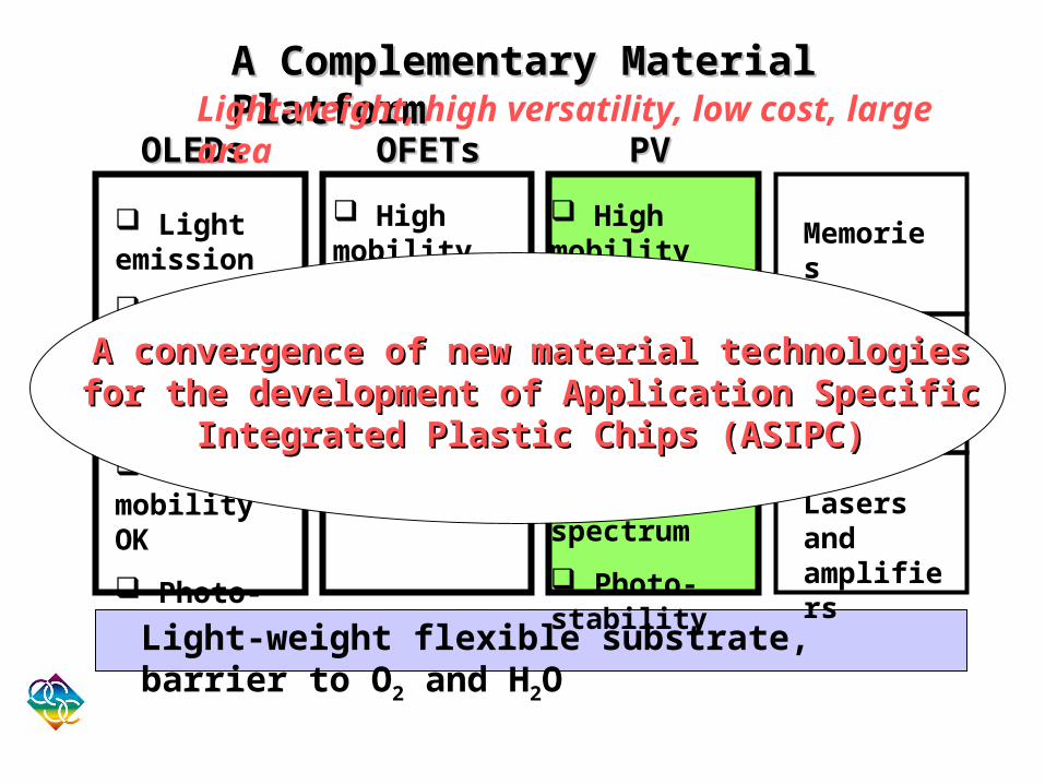
A Complementary Material PlatformA Complementary Material Platform
OLEDsOLEDs
Light emission
High luminescence efficiency
Low mobility OK
Photo-stability
Light-weight flexible substrate, barrier to O2 and H2O
OFETsOFETs PVPV
High mobility
Very thin OK
No condition on optical absorption
High mobility
High photo-generation efficiency
Absorb visible spectrum
Photo-stability
Memories
Electro-optics
Lasers and amplifiers
A convergence of new material technologies for the A convergence of new material technologies for the development of Application Specific Integrated Plastic Chips development of Application Specific Integrated Plastic Chips
(ASIPC)(ASIPC)
Light-weight, high versatility, low cost, large area

Technology OpportunitiesTechnology Opportunities
Efficiency
Low cost
Flexibility
Military
Consumer
Com
mer
cial
Low cost scanners
Optical isolators
Devices that take advantage of the integration of photodetectors on light-weight flexible substrates

Outline
• Introduction to photovoltaic technologies
• Organic excitonic solar cells
• Requirements for conversion with high efficiency
• An approach based on self-assembly
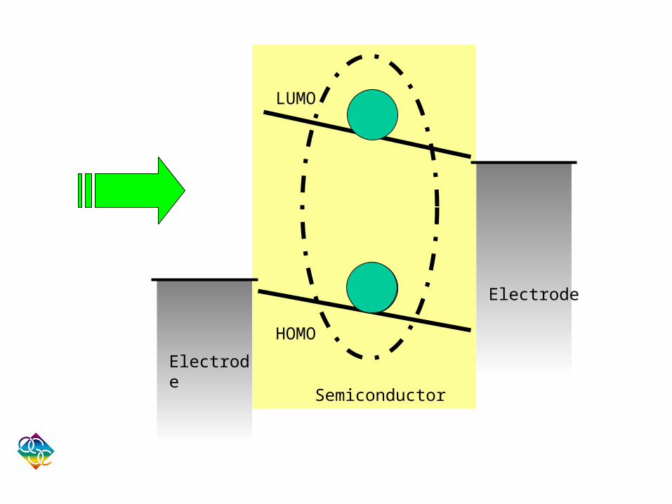
HOMO
LUMO
Electrode
Electrode
Semiconductor

I
V
max SC OC
solar solar
P I VFF
P P
max max
SC OC
I VFF
I V
Solar cell parameters
short-circuit current ISC
open circuit voltage VOC
fill factor FF
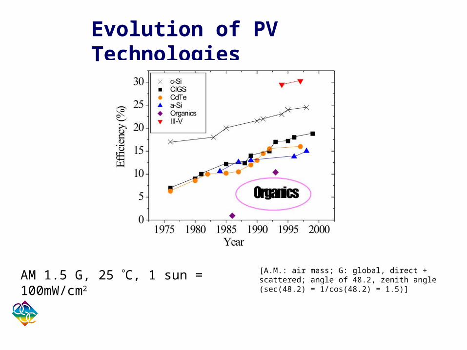
Evolution of PV Technologies
AM 1.5 G, 25 C, 1 sun = 100mW/cm2[A.M.: air mass; G: global, direct + scattered; angle of 48.2, zenith angle (sec(48.2) = 1/cos(48.2) = 1.5)]
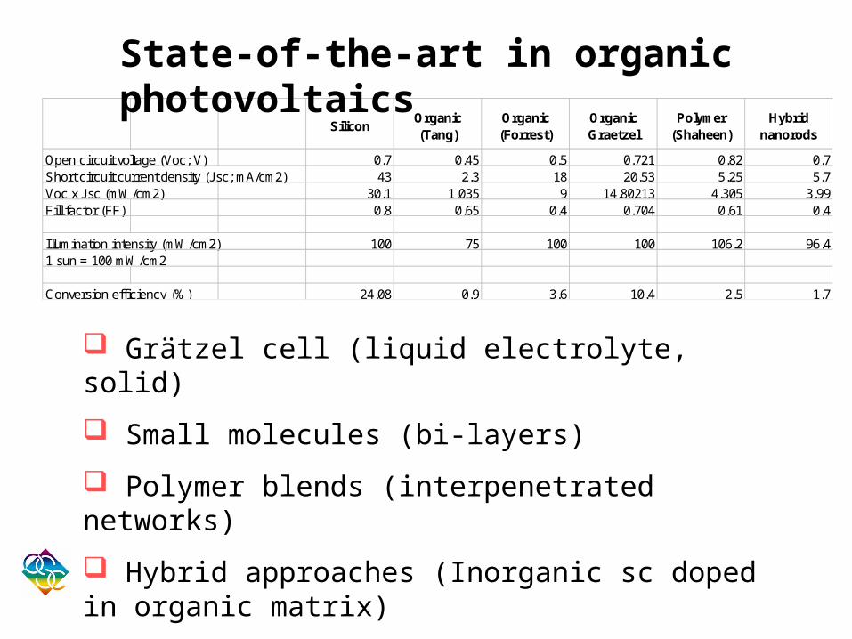
SiliconOrganic (Tang)
Organic (Forrest)
Organic Graetzel
Polymer (Shaheen)
Hybrid nanorods
Open circuit voltage (Voc; V) 0.7 0.45 0.5 0.721 0.82 0.7Short circuit current density (Jsc; mA/cm2) 43 2.3 18 20.53 5.25 5.7Voc x Jsc (mW/cm2) 30.1 1.035 9 14.80213 4.305 3.99Fill factor (FF) 0.8 0.65 0.4 0.704 0.61 0.4
Illumination intensity (mW/cm2) 100 75 100 100 106.2 96.41 sun = 100 mW/cm2
Conversion efficiency (%) 24.08 0.9 3.6 10.4 2.5 1.7
State-of-the-art in organic photovoltaics
Grätzel cell (liquid electrolyte, solid)
Small molecules (bi-layers)
Polymer blends (interpenetrated networks)
Hybrid approaches (Inorganic sc doped in organic matrix)
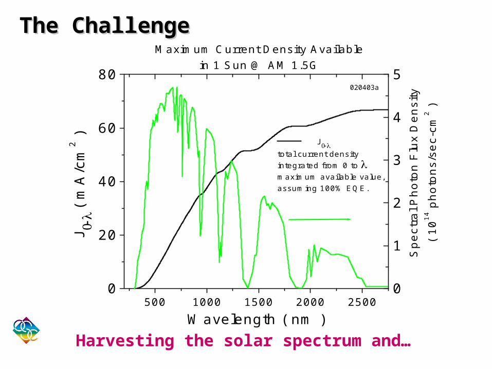
500 1000 1500 2000 25000
20
40
60
80
Maximum Current Density Availablein 1 Sun @ AM 1.5G
J
( m
A/c
m2 )
Wavelength ( nm )
Jtotal current density integrated from 0 to maximum available value, assuming 100% EQE.
0
1
2
3
4
5020403a
Sp
ect
ral P
ho
ton
Flu
x D
en
sity
( 1
014 p
ho
ton
s/se
c-cm
2 )
The ChallengeThe Challenge
Harvesting the solar spectrum and…

optimize absorption, charge generation, charge collection: photocurrent
optimize relative energy levels: built-in voltage
optimize electrical characteristic: fill factor
…maintain simultaneously high open circuit voltage and high fill factor

Step #1: Achieve efficient dissociation of excitons in organic materials
Overcome exciton binding energy
vacuum
electrode
electrode
HOMO
LUMO
Single layer
vacuum
Double layer
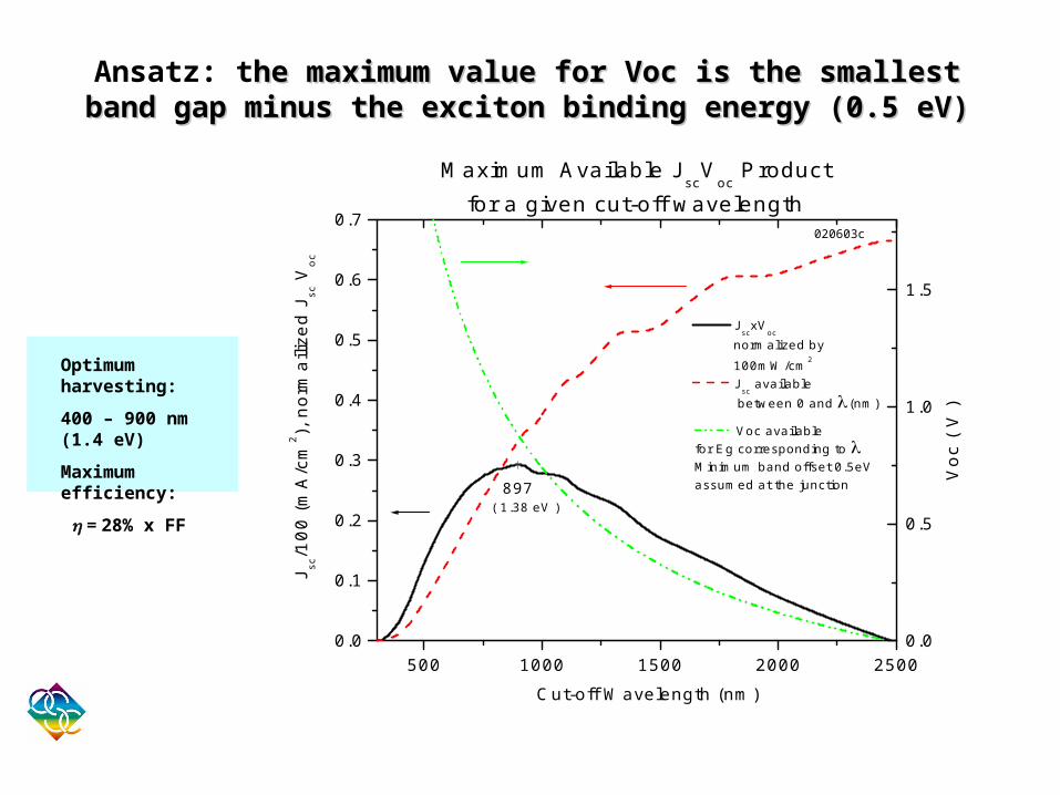
Ansatz: the maximum value for Voc is the smallest band gap he maximum value for Voc is the smallest band gap minus the exciton binding energy (0.5 eV)minus the exciton binding energy (0.5 eV)
500 1000 1500 2000 25000.0
0.1
0.2
0.3
0.4
0.5
0.6
0.7
897
Maximum Available Jsc
Voc
Productfor a given cut-off wavelength
( 1.38 eV )
J sc/1
00
(m
A/c
m2 ),
no
rma
ilize
d J
sc V
oc
Cut-off Wavelength (nm)
Jsc
xVoc
normalized by
100mW/cm2
Jsc
available between 0 and (nm)
0.0
0.5
1.0
1.5
020603c
Voc available for Eg corresponding to Minimum band offset 0.5eV assumed at the junction V
oc
( V
)
Optimum harvesting:
400 – 900 nm (1.4 eV)
Maximum efficiency:
= 28% x FF

500 1000 1500 2000 25000
5
10
15
20
25
30
021003b
Effi
cien
cy (
%)
Cut-off Wavelength (nm)
FF = 1.0 FF = 0.8 FF = 0.7 FF = 0.6 FF = 0.5 FF = 0.4
4 3 2 1 0.5
Energy Gap ( eV )
High Efficiency: Maximize Light Harvesting and Fill High Efficiency: Maximize Light Harvesting and Fill FactorFactor

Equivalent Circuit Model
)(1)exp(
1
10 AR
VJ
nV
AJRVJ
RRJ
Pph
T
S
PS
ARJ
V
J
JVnV
P
OCphTOC
00
1ln
00
)1(1lnJ
J
R
R
J
J
A
nVRJ SC
P
SphTSSC
OPEN-CIRCUIT VOLTAGE
(J=0)
SHORT-CIRCUIT CURRENT DENSITY
(V=0)
Understanding Key Factors for Efficient Organic Photovoltaic Cells
Finite conductance of materials and contact resistance : nonzero Rs
Leakage path : finite Rp
What determines the fill factor ?
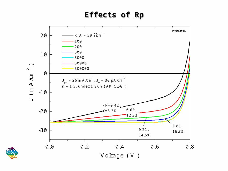
0.0 0.2 0.4 0.6 0.8
-30
-20
-10
0
10
20020603b
0.71,14.5%
0.81,16.8%
0.60,12.3%
FF=0.42,=8.3%
J (
mA
/cm
2 )
Voltage ( V )
RpA = 50 cm2
100 200 500 5000 50000 500000
Jph
= 26 mA/cm2, J0 = 30 pA/cm2
n = 1.5, under 1 Sun ( AM 1.5G )
Effects of RpEffects of Rp

102 103 104 105 1060.95
0.96
0.97
0.98
0.99
1.00
021003c
Effect of Rp on V
oc at Different Photocurrents
Jph
= 26mA/cm2
Jph
= 2.6mA/cm2
J0 = 30pA/cm2, n=1.5
Voc
normalized by the value corresponding to R
p=infinite
No
rma
lize
d V
oc(R
p)
RpA ( cm2 )

0.0 0.2 0.4 0.6 0.8-35
-30
-25
-20
-15
-10
-5
0
5020603a
0.75,15.6%
0.64,13.3%
0.54,11.1 %
FF=0.34,=7.1%
0.81,16.8%
J0 = 30 pA/cm2
Jph
= 26 mA/cm2
n = 1.5
Cur
rent
Den
sity
( m
A/c
m2 )
Voltage ( V )
J(RsA=0 cm2)
J(RsA=2 cm2)
J(RsA=4 cm2)
J(RsA=6 cm2)
J(RsA=8 cm2)
J(RsA=10 cm2)
J(RsA=20 cm2)
Effects of REffects of Rss
A need for high mobility materials
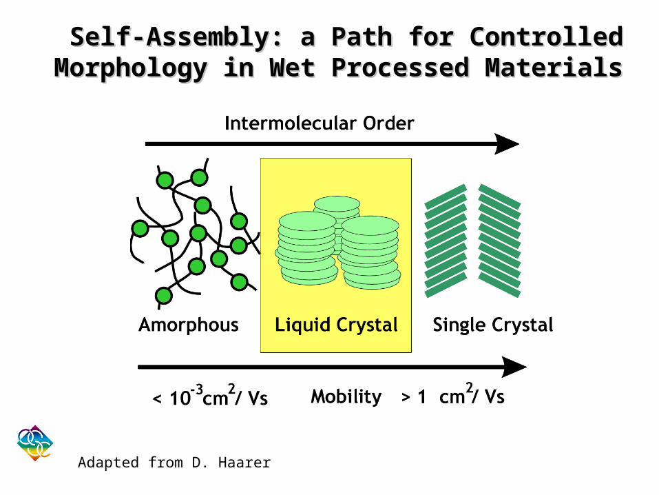
Self-Assembly: a Path for Controlled Morphology in Self-Assembly: a Path for Controlled Morphology in Wet Processed MaterialsWet Processed Materials
Adapted from D. Haarer
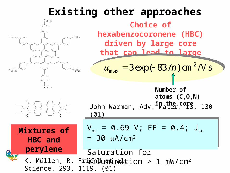
Existing other approachesC12H25
C12H25
C12H25
C12H25
C12H25
C12H25
NN
O
O
O
O
K. Müllen, R. Friend et al. Science, 293, 1119, (01)
Mixtures of HBC and perylene
Voc = 0.69 V; FF = 0.4; Jsc = 30 A/cm2
Saturation for illumination > 1 mW/cm2
Choice of hexabenzocoronene (HBC) driven by large core that
can lead to large mobility
2max 3 exp( 83/ ) cm / Vsn
Number of atoms (C,O,N) in the core
John Warman, Adv. Mater. 13, 130 (01)

Our material’s choice: phthalocyanines
NH
NN
NH
N N
N
N
Good Thermal stabilityGood Thermal stability
Strong Molar absorptivityStrong Molar absorptivity
Good Light stabilityGood Light stability
NH
NNNH
N N
N
N
O
O
OO
OO
O
O
Skoulios et al. J. Am. Chem.Soc. 1982, 104, 5245-5247
e-
e-
e-
e--e
-e
-e
Alkoxy substituted Pc known to form discotic hexagonally ordered mesophases.
Problems: KI > 350°C, difficult to align, no photocurrent when combined with PTCDI

N
NNN
N N
N
N
O
O
O
O
OO
OO
OO
OO
OO
OO
Cu
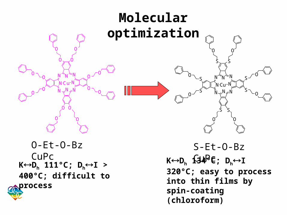
Molecular design
Core:
Metal:
Arms:
Tuning of spectroscopic and electronic properties
Provides large core for strong -orbitals coupling and cohesive forces through Van der Waals interactions
Influence the solid-to-mesophase (KDh) and mesophase-to-isotropic liquid (DhI) transition temperatures
NNN
N
N N
N
N
S
O
S
O
S
O
S
O
SO
SO
SO
SO
CuN
NNN
N N
N
N
O
O
O
O
O
O
O
O
OO
OO
OO
OO
Cu
S-Et-O-Bz CuPcO-Et-O-Bz CuPc
Molecular optimization
KDh 111°C; DhI > 400°C; difficult to process
KDh 134°C; DhI 320°C; easy to process into thin films by spin-coating (chloroform)
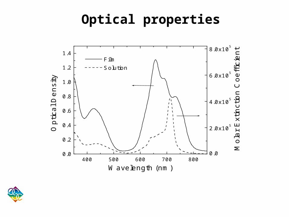
Optical properties
400 500 600 700 8000.0
0.2
0.4
0.6
0.8
1.0
1.2
1.4
Opt
ical
Den
sity
Wavelength (nm)
Film
0.0
2.0x10⁵
4.0x10⁵
6.0x10⁵
8.0x10⁵
Solution
Mol
ar E
xtin
ctio
n C
oeffi
cien
t
Material CharacterizationMaterial Characterization
3 4 5 6 70
2000
4000
6000
8000
10000
12000
14000020303a
XRD of Spin-Coated Films on ITO
Co
un
ts/S
ec
2 theta
20nm 20nm Annealed ITO BK
d
Substrate
d
Substrate
Small-angle X-ray scatteringSmall-angle X-ray scattering
d
Substrate
Data show that Pc form three different types of crystalline phases; dependent on surface treatment

Before annealing
After annealing
AFM studies
Spin-coated at 4000 rpm on PEDOT:PSS/ITO; 180°C for two hrs.
Possibility to form nanostructured surfaces by thermal annealing to create high area networks for improved exciton dissociation
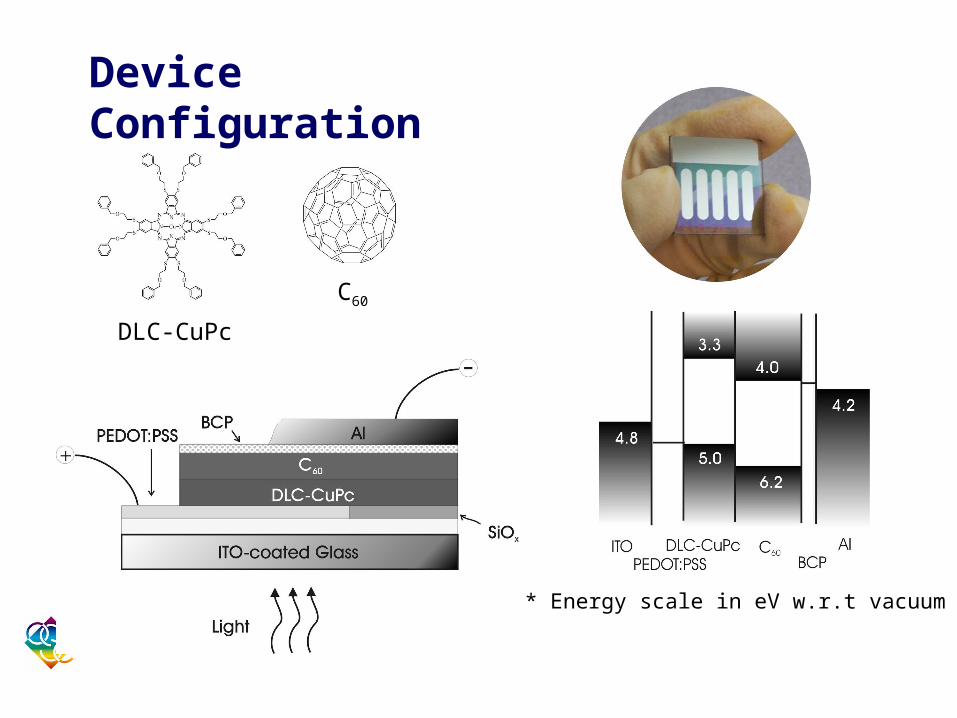
Device Configuration
DLC-CuPc
C60
* Energy scale in eV w.r.t vacuum
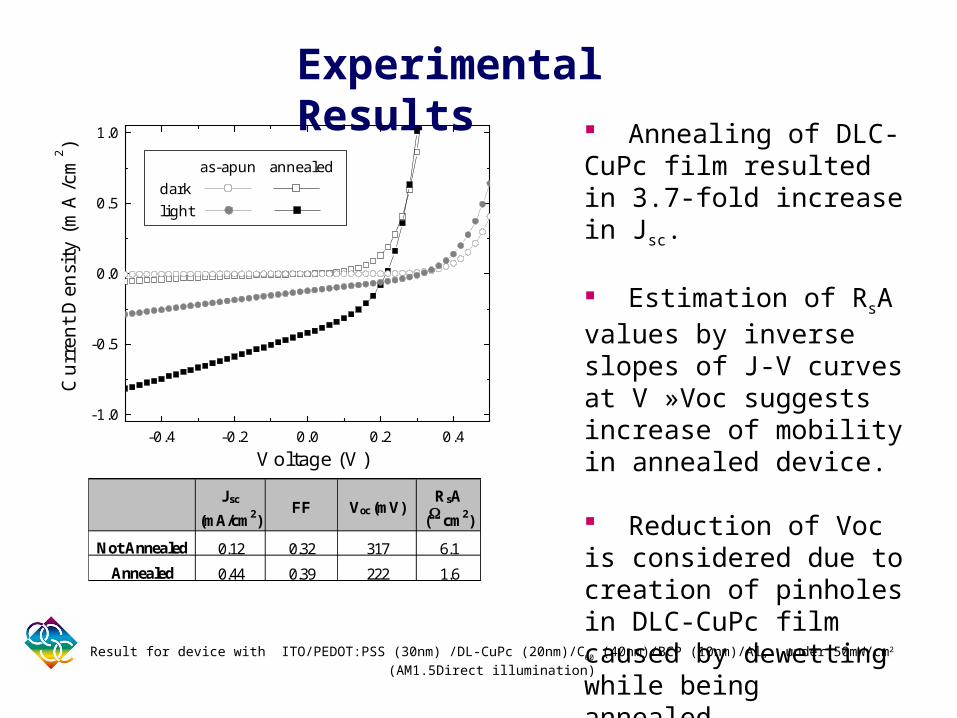
Experimental Results
-0.4 -0.2 0.0 0.2 0.4-1.0
-0.5
0.0
0.5
1.0
Cur
rent
Den
sity
(m
A/c
m2 )
Voltage (V)
as-apun annealeddark light
Annealing of DLC-CuPc film resulted in 3.7-fold increase in Jsc.
Estimation of RsA values by inverse slopes of J-V curves at V »Voc suggests increase of mobility in annealed device.
Reduction of Voc is considered due to creation of pinholes in DLC-CuPc film caused by dewetting while being annealed.
Jsc
(mA/cm2)FF Voc (mV)
RsA
(cm2)
Not Annealed 0.12 0.32 317 6.1
Annealed 0.44 0.39 222 1.6
Result for device with ITO/PEDOT:PSS (30nm) /DL-CuPc (20nm)/C60 (40nm)/BCP (10nm)/Al, under 50mW/cm2 (AM1.5Direct illumination)

e-
e-
e-
e--e
-e
-e
Self-assembled electron transport materialsSelf-assembled electron transport materials
ONN
O
NN
O
NN
OC8H17
OC8H17
C8H17O
OC8H17
OC8H17
OC8H17C8H17O
C8H17O
C8H17O
“Star-like” discotic LC oxadiazole materials with
good electron mobility
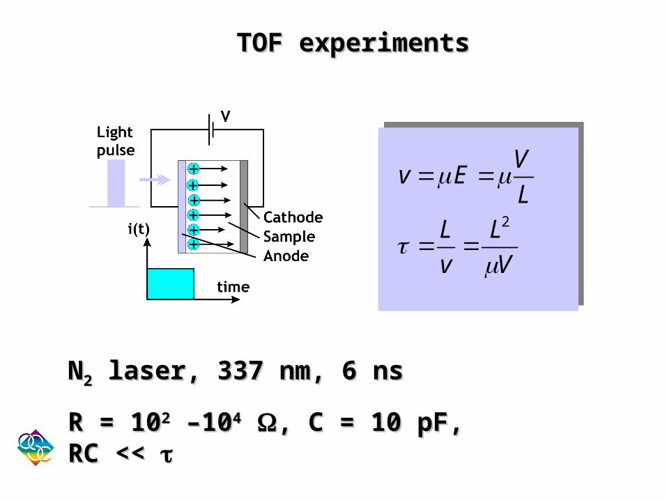
TOF experimentsTOF experiments
2
Vv E
L
L L
v V
NN22 laser, 337 nm, 6 ns laser, 337 nm, 6 ns
R = 10R = 1022 –10 –1044 , C = 10 pF, RC , C = 10 pF, RC << <<
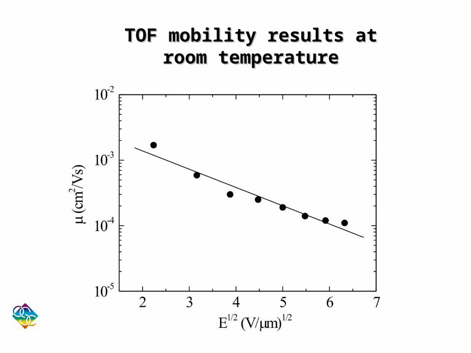
TOF mobility results at TOF mobility results at room temperatureroom temperature

Cyclicvoltammetry of Discotic LCs
-6 10-6
-4 10-6
-2 10-6
0
2 10-6
4 10-6
-2000-1600-1200-800-4000
Triazine versus Fc
potential, mV
-1.5 10-5
-1 10-5
-5 10-6
0
5 10-6
1 10-5
-2000-1500-1000-5000
DLCOX5 versus Fc
potential, mV
ON
N
O
NNO
N N
R2
R1 R3
R2
R1
R3
R2R1
R3 N
NN
ON
N
R2
R1 R3
O
NN
R2
R1
R3
O
N N
R2R1
R3
0.6 volt shift in reduction potentional

OE Testing Facilities
Fully automated high vacuum deposition system with four organic sources and two high power sources for metals and oxides (co-deposition capabilities). Integrated with double glove box (one dry and one wet with integrated spin-coater).

Conclusions and future work
Transport properties of organic semiconductors often limit power conversion efficiency in organic solar cells. High mobility required in materials that can be processed from solution.
DLC-CuPc is solution-processible, and we demonstrated that its transport property can be improved in the discotic liquid crystalline phase.
Photocurrents reaching mA/cm2, significant improvement over HBC-based devices Development of discotic electron-transport oxadiazole-based materials.
Optimization of parameters will require control of interfaces, relative orbital energies, control of morphology through use of self-assembly.

Additional supporting informationAdditional supporting information
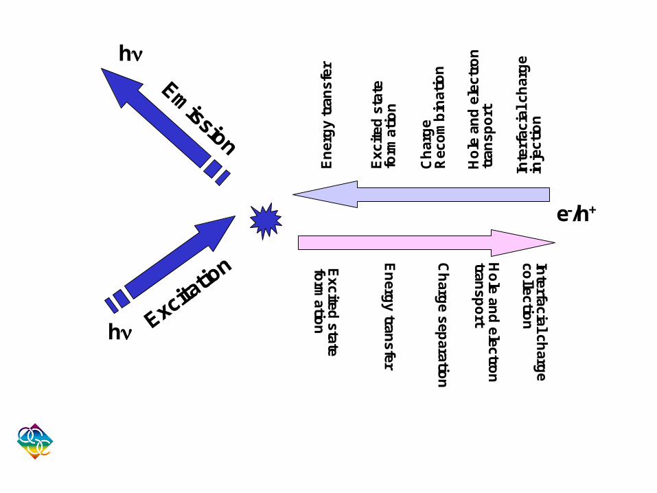
e-/h+
Inte
rfac
ial
char
ge
inje
ctio
n
Ho
le a
nd
ele
ctro
ntr
ansp
ort
Ch
arg
eR
eco
mb
inat
ion
Excited
statefo
rmatio
n
En
ergy tran
sfer
En
erg
y tr
ansf
er
Exc
ited
sta
tefo
rmat
ion
Ch
arge sep
aration
Interfacia l ch
ar ge
collectio
n
Ho
le and
electron
transp
ort
h
h
Emission
Excitatio
n

Stabilization of geometry and patterning
O
O
O
O
254 nm
Photo-crosslinking between adjacent side chains through cyclobutane links; > 50 % conversion of styryl groups
70nm
0nm
100m
8 m2m8 m
a b
150m
0nm
100nm100nm
150m
bare Si

0.0 0.2 0.4 0.6 0.8-35
-30
-25
-20
-15
-10
-5
0
5020603a
0.75,15.6%
0.64,13.3%
0.54,11.1 %
FF=0.34,=7.1%
0.81,16.8%
J0 = 30 pA/cm2
Jph
= 26 mA/cm2
n = 1.5
Cur
rent
Den
sity
( m
A/c
m2 )
Voltage ( V )
J(RsA=0 cm2)
J(RsA=2 cm2)
J(RsA=4 cm2)
J(RsA=6 cm2)
J(RsA=8 cm2)
J(RsA=10 cm2)
J(RsA=20 cm2)
0.0 0.2 0.4 0.6 0.8
-30
-20
-10
0
10
20020603b
0.71,14.5%
0.81,16.8%
0.60,12.3%
FF=0.42,=8.3%
J (
mA
/cm
2 )Voltage ( V )
RpA = 50 cm2
100 200 500 5000 50000 500000
Jph
= 26 mA/cm2, J0 = 30 pA/cm2
n = 1.5, under 1 Sun ( AM 1.5G )
Effects of REffects of Rss and R and Rpp on Fill Factor in High on Fill Factor in High
Photocurrent RegimePhotocurrent Regime
Minimize RMinimize Rss and Maximize R and Maximize Rpp

Excitonic Solar Cells: Energy Level EngineeringExcitonic Solar Cells: Energy Level Engineering
Vacuum level
EA
IpE
EHTL
ETL
A) B)
C) D)
Band offset < exciton binding energy
Band offset > exciton binding energy
Working hypothesis: the maximum value for Vthe maximum value for Vococ is the smallest is the smallest
band gap minus the exciton binding energy (0.5 eV)band gap minus the exciton binding energy (0.5 eV)
10 100 10000.6
0.7
0.8
0.9
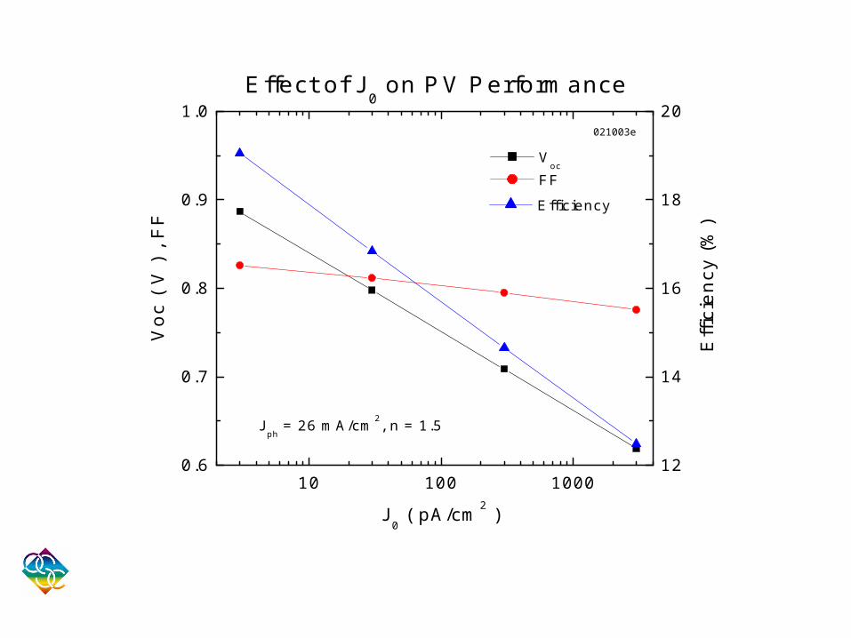
1.0Effect of J
0 on PV Performance
Jph
= 26 mA/cm2, n = 1.5
Vo
c (
V )
, F
F
J0 ( pA/cm2 )
Voc
FF
12
14
16
18
20021003e
Eff
icie
ncy
(%)
Efficiency