Embed Size (px)
Citation preview
journal homepage: www.elsevier.com/locate/nanoenergy
Available online at www.sciencedirect.com
REVIEW
Plasmonic nano-lasers
Yin Yina, Teng Qiua,b,n, Jiaqi Lia, Paul K. Chub,nn
aDepartment of Physics, Southeast University, Nanjing 211189, PR ChinabDepartment of Physics and Materials Science, City University of Hong Kong, Tat Chee Avenue, Kowloon, Hong Kong, PR ChinaAvailable online 17 October 2011
KEYWORDSPlasmonics;Nano-laser;Nano-energy;Resonant cavity;Dark mode
AbstractDevelopment of a coherent, intense, ultrafast source of optical energy focused to a nano-scalearea enables the integration of thousands of them on a single chip to power an optical computer.Very intense, ultrafast, temporarily coherent pulses of nano-localized optical fields are thus offundamental interest and have many applications in integrated nano-photonics. This paperreviews the mechanism associated with plasmonic nano-lasers and general guidelines pertainingto device design. Recent results show that a plasmonic nano-laser effectively overcomes manyof the difficulties and limitations of plasmonics and has enormous potential in sub-wavelengthphotonic circuits and fundamental investigation of single-molecular events. Future challengesand research directions are also discussed.& 2011 Elsevier Ltd. All rights reserved.
Introduction
Lasers first experimentally demonstrated by Schawlow andTownes [1] are among the most important inventions in the20th century. The ability to generate intense and coherentoptical energy has spurred ground breaking research activ-ities in micro- and nano-scale materials in the past decades.Deeper exploration of the micro- and nano-world requiresextremely small, ultrafast, and coherent laser sources toconcentrate optical energy into regions with sub-wavelengthdimensions. However, advances have been hampered byconventional light sources because their size is constrained bythe diffraction limit. Although some devices offer near-fieldoptical energy [2–5] by adopting exit apertures with nano-
dimensions, photon transport in the nanostructures is still notwell understood. A nano-laser possessing a tiny cavity has amuch smaller physical scale than a traditional laser andphotonic crystals [6] have been developed to address thediffraction limitation. However, since conventional lasers arebased on optical pumping and stimulated emission, it isdifficult to produce a nano-scale cavity and overcome thediffraction limitation so that a beam of light with size smallerthan its wavelength can be generated.
A plasmonic nano-laser is different from a conventionallaser in that surface plasmons (SPs) instead of photons areused to amplify the radiation by stimulated emission [7].SPs, a near-field phenomenon of surface electron oscilla-tions, originate from the interactions between incidentelectromagnetic (EM) field and free electrons in metals suchas silver and gold. The resonant excitations on the micro- ornano-scale metal structures tend to form highly localized SPwith large EM field enhancement effects and good spatialconfinement on the sub-wavelength scale, thus avoidingthe limitation imposed by diffraction. In particular, the
2211-2855/$ - see front matter & 2011 Elsevier Ltd. All rights reserved.doi:10.1016/j.nanoen.2011.09.002
nCorresponding author. Tel.: +86 25 52090600 8210;fax: +86 25 52090600 8204.
nnCorresponding author. Tel.: +852 34427724; fax: +852 34420542.E-mail addresses: [email protected] (T. Qiu),
[email protected] (P.K. Chu).
Nano Energy (2012) 1, 25–41
nano-scale interface between a dielectric and metal supportssome special EM modes such as SP polariton (SPP). SPPpropagating along the interface is a transverse magneticpolarized optical surface wave bounded by the metal–dielectric border via coupling between the EM and long-itudinal surface charge density oscillations in the metal [8].When light irradiates the metal–dielectric interface, oscilla-tions of free electrons in the metal are hindered by thedielectric border, which prevents the electrons from enteringand forces them to move in waves along the nano-scale metal–dielectric interface. Meanwhile, a metal nanostructure with alarge light absorption cross section is capable of confining theresonant energy into the localized nano-area by collectiveelectron oscillations. The highly localized optical fields fromSPs are confined into tiny spots with nano- or sub-wavelengthdimensions. While traditional lasers suffer from diffractioneffects in this size regime, the strong localized enhancementand sub-wavelength confinement lead to spatial localization indimensions well below the diffraction limit thus making nano-scale integrated photonic circuits possible [9–12]. For example,Stockman has theoretically predicted SPPs propagation in atapered plasmonic waveguide [13]. Rapid adiabatic nano-focusing of energy in three dimensions takes place on the tipand the local field and energy density are increased by threefolds and orders of magnitude, respectively. In a plasmonicnano-laser, electron oscillations are coupled directly with thelocalized optical modes and the coupling can be modulated bythe dielectric environment as well as size and shape of themetal nanostructures. Consequently, the low coupling effi-ciency and unavailability of individual optical modes can becircumvented.
The gain medium, which is an essential part of atraditional laser serving as the pumping and resonancecavity, plays a likewise important role in a nano-laser inorder to maintain the population inversion in the multilevelsystem. The resonant cavity which serves to stimulate morelight emission with the same phase by reflecting the lightback and forth in a traditional laser is substituted by metalnanostructures such as nano-shells [14,15] in order togenerate the initial SPs around the nano-scale metal–
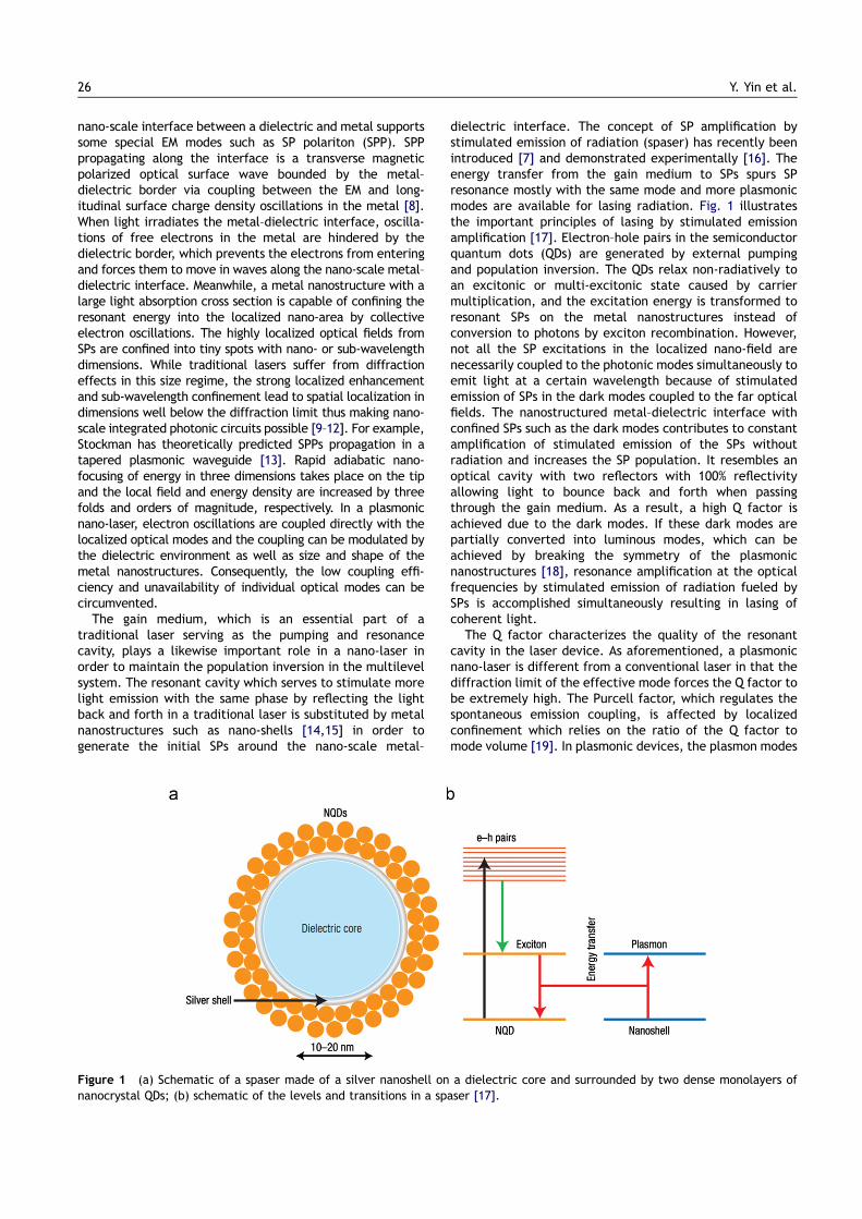
dielectric interface. The concept of SP amplification bystimulated emission of radiation (spaser) has recently beenintroduced [7] and demonstrated experimentally [16]. Theenergy transfer from the gain medium to SPs spurs SPresonance mostly with the same mode and more plasmonicmodes are available for lasing radiation. Fig. 1 illustratesthe important principles of lasing by stimulated emissionamplification [17]. Electron–hole pairs in the semiconductorquantum dots (QDs) are generated by external pumpingand population inversion. The QDs relax non-radiatively toan excitonic or multi-excitonic state caused by carriermultiplication, and the excitation energy is transformed toresonant SPs on the metal nanostructures instead ofconversion to photons by exciton recombination. However,not all the SP excitations in the localized nano-field arenecessarily coupled to the photonic modes simultaneously toemit light at a certain wavelength because of stimulatedemission of SPs in the dark modes coupled to the far opticalfields. The nanostructured metal–dielectric interface withconfined SPs such as the dark modes contributes to constantamplification of stimulated emission of the SPs withoutradiation and increases the SP population. It resembles anoptical cavity with two reflectors with 100% reflectivityallowing light to bounce back and forth when passingthrough the gain medium. As a result, a high Q factor isachieved due to the dark modes. If these dark modes arepartially converted into luminous modes, which can beachieved by breaking the symmetry of the plasmonicnanostructures [18], resonance amplification at the opticalfrequencies by stimulated emission of radiation fueled bySPs is accomplished simultaneously resulting in lasing ofcoherent light.
The Q factor characterizes the quality of the resonantcavity in the laser device. As aforementioned, a plasmonicnano-laser is different from a conventional laser in that thediffraction limit of the effective mode forces the Q factor tobe extremely high. The Purcell factor, which regulates thespontaneous emission coupling, is affected by localizedconfinement which relies on the ratio of the Q factor tomode volume [19]. In plasmonic devices, the plasmon modes
Figure 1 (a) Schematic of a spaser made of a silver nanoshell on a dielectric core and surrounded by two dense monolayers ofnanocrystal QDs; (b) schematic of the levels and transitions in a spaser [17].
Y. Yin et al.26
have mode volumes that break the diffraction limit, andthus a high Purcell enhancement as well as good confine-ment factor can be achieved in spite of a smaller Q factor.Therefore, operation of a plasmonic nano-laser with a smallQ factor is possible. For instance, a low-threshold or no-threshold laser can be achieved due to the high Purcellenhancement because preferential emission may be coupledto a special lasing mode to further enhance the efficiency ofstimulated emission [20]. Ultrafast generation and amplifi-cation of SPs for lasing can be modulated at frequencies upto terahertz on account of the Purcell enhancement.Despite limitation by the metal absorption loss, theplasmonic modes have a broad band and enhance emissionover a large bandwidth [14].
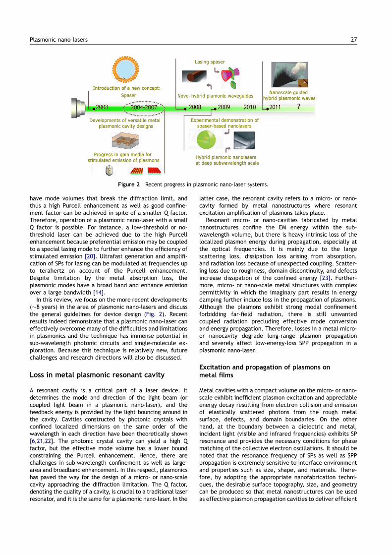
In this review, we focus on the more recent developments(�8 years) in the area of plasmonic nano-lasers and discussthe general guidelines for device design (Fig. 2). Recentresults indeed demonstrate that a plasmonic nano-laser caneffectively overcome many of the difficulties and limitationsin plasmonics and the technique has immense potential insub-wavelength photonic circuits and single-molecule ex-ploration. Because this technique is relatively new, futurechallenges and research directions will also be discussed.
Loss in metal plasmonic resonant cavity
A resonant cavity is a critical part of a laser device. Itdetermines the mode and direction of the light beam (orcoupled light beam in a plasmonic nano-laser), and thefeedback energy is provided by the light bouncing around inthe cavity. Cavities constructed by photonic crystals withconfined localized dimensions on the same order of thewavelength in each direction have been theoretically shown[6,21,22]. The photonic crystal cavity can yield a high Qfactor, but the effective mode volume has a lower boundconstraining the Purcell enhancement. Hence, there arechallenges in sub-wavelength confinement as well as large-area and broadband enhancement. In this respect, plasmonicshas paved the way for the design of a micro- or nano-scalecavity approaching the diffraction limitation. The Q factor,denoting the quality of a cavity, is crucial to a traditional laserresonator, and it is the same for a plasmonic nano-laser. In the
latter case, the resonant cavity refers to a micro- or nano-cavity formed by metal nanostructures where resonantexcitation amplification of plasmons takes place.
Resonant micro- or nano-cavities fabricated by metalnanostructures confine the EM energy within the sub-wavelength volume, but there is heavy intrinsic loss of thelocalized plasmon energy during propagation, especially atthe optical frequencies. It is mainly due to the largescattering loss, dissipation loss arising from absorption,and radiation loss because of unexpected coupling. Scatter-ing loss due to roughness, domain discontinuity, and defectsincrease dissipation of the confined energy [23]. Further-more, micro- or nano-scale metal structures with complexpermittivity in which the imaginary part results in energydamping further induce loss in the propagation of plasmons.Although the plasmons exhibit strong modal confinementforbidding far-field radiation, there is still unwantedcoupled radiation precluding effective mode conversionand energy propagation. Therefore, losses in a metal micro-or nanocavity degrade long-range plasmon propagationand severely affect low-energy-loss SPP propagation in aplasmonic nano-laser.
Excitation and propagation of plasmons onmetal films
Metal cavities with a compact volume on the micro- or nano-scale exhibit inefficient plasmon excitation and appreciableenergy decay resulting from electron collision and emissionof elastically scattered photons from the rough metalsurface, defects, and domain boundaries. On the otherhand, at the boundary between a dielectric and metal,incident light (visible and infrared frequencies) exhibits SPresonance and provides the necessary conditions for phasematching of the collective electron oscillations. It should benoted that the resonance frequency of SPs as well as SPPpropagation is extremely sensitive to interface environmentand properties such as size, shape, and materials. There-fore, by adopting the appropriate nanofabrication techni-ques, the desirable surface topography, size, and geometrycan be produced so that metal nanostructures can be usedas effective plasmon propagation cavities to deliver efficient
Figure 2 Recent progress in plasmonic nano-laser systems.
Plasmonic nano-lasers 27
SP excitation and propagation of SPP with lower energydissipation. Both are crucial to photonic integrated circuitsand devices.
The wave vector of the SPP is obtained by solvingMaxwell’s equations at the planar metal–dielectricboundary:
kSPP ¼ k0e1e2e1þe2
� �1=2
ð1Þ
where kSPP is the wave vector of the SPP, k0 is the wavevector of the incident EM wave, and e1 and e2 are thepermittivity values of the dielectrics and metal, respec-tively (9e294e1 and the real part of e2o0). Considering therelationship between the wave vectors of the incident light,reflected light, and transmitted light, the wave vector ofthe SPP is always larger than that available to the incidentplane waves in the adjacent dielectric medium. Thedispersion curve of the SPs always lies outside the lightcone and therefore, plane light waves cannot excite the SPPdirectly.
In order to enhance the efficiency of SPP excitation, anattenuated total reflection setup has been proposed togenerate collective electron oscillations and detect thepropagation of SPP [8]. Using a prism in an attenuated totalreflection arrangement on glass attached to a metal film, anincident light beam with angles below the total internalreflection contributes to an evanescent wave with a wavevector that may match that of the propagating SPP at themetal/air interface. Noble metal films are promising in theguiding and propagation of plasmons [24] and metal filmswith simple structures can also be easily attached to thedevices for effective plasmon excitation.
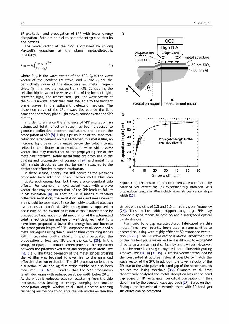
In these setups, energy loss still occurs as the plasmonspropagate back into the prism. Thicker metal films canmitigate such energy loss, but there are concomitant sideeffects. For example, an evanescent wave with a wavevector that may not match that of the SPP leads to failurein SP excitation [8]. In addition, as a means of far-fieldcollective excitation, the excitation area and measurementarea should be separated. Since the highly localized electronoscillations are confined, SPP propagation is supposed tooccur outside the excitation region without interference byunexpected light modes. Slight modulation of the attenuatedtotal reflection prism and use of well-designed metal filmshave been proposed to lower the energy loss and increasethe propagation length of SPP. Lamprecht et al. developed ametal waveguide using thin Au and Ag films containing stripeswith micrometer widths (1–54 mm) and investigated thepropagation of localized SPs along the cavity [25]. In thissetup, an opaque aluminum screen provided the separationbetween the plasmon excitation and propagation areas (seeFig. 3(a)). The tilted geometry of the metal stripes crossingthe Al film was believed to give rise to the enhancedeffective plasmon excitation. The SPP propagation length asa function of Au and Ag film stripe widths has also beenmeasured. Fig. 3(b) illustrates that the SPP propagationlength decreases with reduced Ag stripe width below 20 mm.As the width is reduced, plasmon scattering from the sideincreases, thus leading to energy damping and smallerpropagation length. Weeber et al. used a photon scanningtunneling microscope to observe the SPP modes on thin film
stripes with widths of 2.5 and 3.5 mm at a visible frequency[26]. These stripes which support long-range SPP mayprovide a good means to develop noble integrated opticalcavity devices.
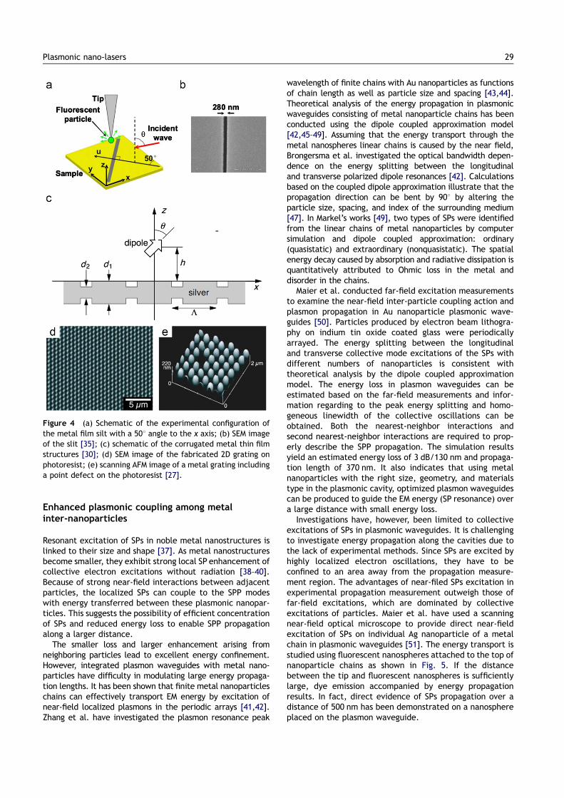
Plasmonic band-gap nanostructures fabricated on thinmetal films have recently been used as nano-cavities toaccomplish lasing with highly efficient SP resonance excita-tion [27–30]. The SPP wave vector is always larger than thatof the incident plane waves and so it is difficult to excite SPPdirectly on a planar metal surface by plane waves. However,it can be remedied using corrugated metal films with gratinggrooves (see Fig. 4) [31–35]. A grating vector introduced bythe corrugated structures makes it possible to match thewave vector of the SPP. In addition, the lower velocity of theSPs due to the wide plasmonic band gap of the nanostructuresreduces the lasing threshold [36]. Okamoto et al. havetheoretically analyzed the metal absorption loss at the bandgap edges of 1D rectangular periodical corrugations in thinsilver films by the coupled-wave approach [27]. Based on theirfindings, the behavior of plasmonic lasers with 2D band gapstructures can be predicted.
Figure 3 (a) Schematic of the experimental setup of spatiallyconfined SPs excitation; (b) experimentally obtained SPPspropagation length in 70-nm-thick silver stripes versus stripewidth [25].
Y. Yin et al.28
Enhanced plasmonic coupling among metalinter-nanoparticles
Resonant excitation of SPs in noble metal nanostructures islinked to their size and shape [37]. As metal nanostructuresbecome smaller, they exhibit strong local SP enhancement ofcollective electron excitations without radiation [38–40].Because of strong near-field interactions between adjacentparticles, the localized SPs can couple to the SPP modeswith energy transferred between these plasmonic nanopar-ticles. This suggests the possibility of efficient concentrationof SPs and reduced energy loss to enable SPP propagationalong a larger distance.
The smaller loss and larger enhancement arising fromneighboring particles lead to excellent energy confinement.However, integrated plasmon waveguides with metal nano-particles have difficulty in modulating large energy propaga-tion lengths. It has been shown that finite metal nanoparticleschains can effectively transport EM energy by excitation ofnear-field localized plasmons in the periodic arrays [41,42].Zhang et al. have investigated the plasmon resonance peak
wavelength of finite chains with Au nanoparticles as functionsof chain length as well as particle size and spacing [43,44].Theoretical analysis of the energy propagation in plasmonicwaveguides consisting of metal nanoparticle chains has beenconducted using the dipole coupled approximation model[42,45–49]. Assuming that the energy transport through themetal nanospheres linear chains is caused by the near field,Brongersma et al. investigated the optical bandwidth depen-dence on the energy splitting between the longitudinaland transverse polarized dipole resonances [42]. Calculationsbased on the coupled dipole approximation illustrate that thepropagation direction can be bent by 901 by altering theparticle size, spacing, and index of the surrounding medium[47]. In Markel’s works [49], two types of SPs were identifiedfrom the linear chains of metal nanoparticles by computersimulation and dipole coupled approximation: ordinary(quasistatic) and extraordinary (nonquasistatic). The spatialenergy decay caused by absorption and radiative dissipation isquantitatively attributed to Ohmic loss in the metal anddisorder in the chains.
Maier et al. conducted far-field excitation measurementsto examine the near-field inter-particle coupling action andplasmon propagation in Au nanoparticle plasmonic wave-guides [50]. Particles produced by electron beam lithogra-phy on indium tin oxide coated glass were periodicallyarrayed. The energy splitting between the longitudinaland transverse collective mode excitations of the SPs withdifferent numbers of nanoparticles is consistent withtheoretical analysis by the dipole coupled approximationmodel. The energy loss in plasmon waveguides can beestimated based on the far-field measurements and infor-mation regarding to the peak energy splitting and homo-geneous linewidth of the collective oscillations can beobtained. Both the nearest-neighbor interactions andsecond nearest-neighbor interactions are required to prop-erly describe the SPP propagation. The simulation resultsyield an estimated energy loss of 3 dB/130 nm and propaga-tion length of 370 nm. It also indicates that using metalnanoparticles with the right size, geometry, and materialstype in the plasmonic cavity, optimized plasmon waveguidescan be produced to guide the EM energy (SP resonance) overa large distance with small energy loss.
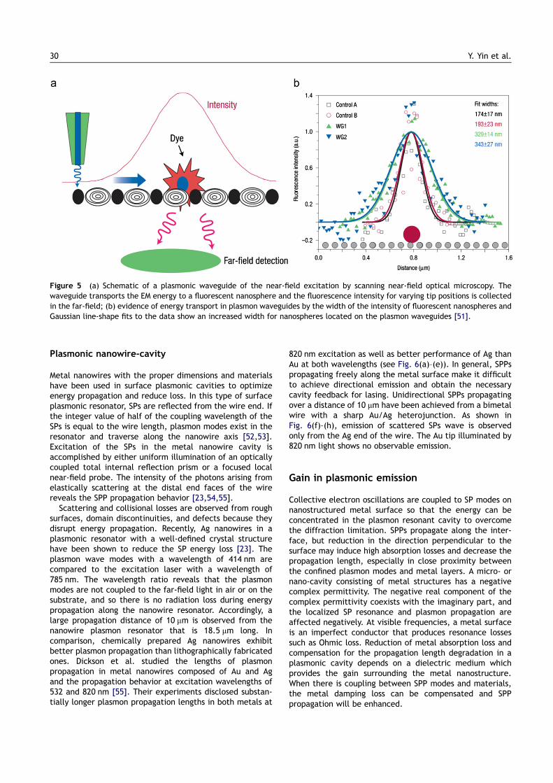
Investigations have, however, been limited to collectiveexcitations of SPs in plasmonic waveguides. It is challengingto investigate energy propagation along the cavities due tothe lack of experimental methods. Since SPs are excited byhighly localized electron oscillations, they have to beconfined to an area away from the propagation measure-ment region. The advantages of near-filed SPs excitation inexperimental propagation measurement outweigh those offar-field excitations, which are dominated by collectiveexcitations of particles. Maier et al. have used a scanningnear-field optical microscope to provide direct near-fieldexcitation of SPs on individual Ag nanoparticle of a metalchain in plasmonic waveguides [51]. The energy transport isstudied using fluorescent nanospheres attached to the top ofnanoparticle chains as shown in Fig. 5. If the distancebetween the tip and fluorescent nanospheres is sufficientlylarge, dye emission accompanied by energy propagationresults. In fact, direct evidence of SPs propagation over adistance of 500 nm has been demonstrated on a nanosphereplaced on the plasmon waveguide.
Figure 4 (a) Schematic of the experimental configuration ofthe metal film silt with a 501 angle to the x axis; (b) SEM imageof the slit [35]; (c) schematic of the corrugated metal thin filmstructures [30]; (d) SEM image of the fabricated 2D grating onphotoresist; (e) scanning AFM image of a metal grating includinga point defect on the photoresist [27].
Plasmonic nano-lasers 29
Plasmonic nanowire-cavity
Metal nanowires with the proper dimensions and materialshave been used in surface plasmonic cavities to optimizeenergy propagation and reduce loss. In this type of surfaceplasmonic resonator, SPs are reflected from the wire end. Ifthe integer value of half of the coupling wavelength of theSPs is equal to the wire length, plasmon modes exist in theresonator and traverse along the nanowire axis [52,53].Excitation of the SPs in the metal nanowire cavity isaccomplished by either uniform illumination of an opticallycoupled total internal reflection prism or a focused localnear-field probe. The intensity of the photons arising fromelastically scattering at the distal end faces of the wirereveals the SPP propagation behavior [23,54,55].
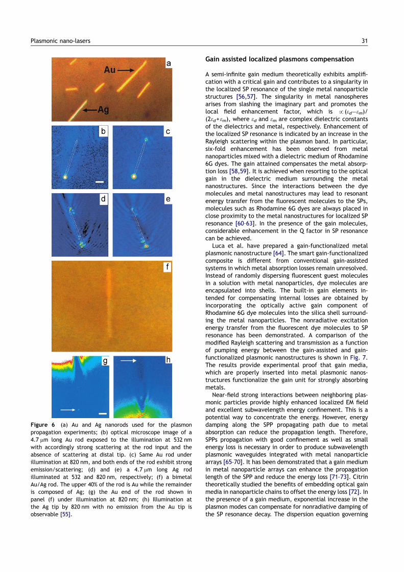
Scattering and collisional losses are observed from roughsurfaces, domain discontinuities, and defects because theydisrupt energy propagation. Recently, Ag nanowires in aplasmonic resonator with a well-defined crystal structurehave been shown to reduce the SP energy loss [23]. Theplasmon wave modes with a wavelength of 414 nm arecompared to the excitation laser with a wavelength of785 nm. The wavelength ratio reveals that the plasmonmodes are not coupled to the far-field light in air or on thesubstrate, and so there is no radiation loss during energypropagation along the nanowire resonator. Accordingly, alarge propagation distance of 10 mm is observed from thenanowire plasmon resonator that is 18.5 mm long. Incomparison, chemically prepared Ag nanowires exhibitbetter plasmon propagation than lithographically fabricatedones. Dickson et al. studied the lengths of plasmonpropagation in metal nanowires composed of Au and Agand the propagation behavior at excitation wavelengths of532 and 820 nm [55]. Their experiments disclosed substan-tially longer plasmon propagation lengths in both metals at
820 nm excitation as well as better performance of Ag thanAu at both wavelengths (see Fig. 6(a)–(e)). In general, SPPspropagating freely along the metal surface make it difficultto achieve directional emission and obtain the necessarycavity feedback for lasing. Unidirectional SPPs propagatingover a distance of 10 mm have been achieved from a bimetalwire with a sharp Au/Ag heterojunction. As shown inFig. 6(f)–(h), emission of scattered SPs wave is observedonly from the Ag end of the wire. The Au tip illuminated by820 nm light shows no observable emission.
Gain in plasmonic emission
Collective electron oscillations are coupled to SP modes onnanostructured metal surface so that the energy can beconcentrated in the plasmon resonant cavity to overcomethe diffraction limitation. SPPs propagate along the inter-face, but reduction in the direction perpendicular to thesurface may induce high absorption losses and decrease thepropagation length, especially in close proximity betweenthe confined plasmon modes and metal layers. A micro- ornano-cavity consisting of metal structures has a negativecomplex permittivity. The negative real component of thecomplex permittivity coexists with the imaginary part, andthe localized SP resonance and plasmon propagation areaffected negatively. At visible frequencies, a metal surfaceis an imperfect conductor that produces resonance lossessuch as Ohmic loss. Reduction of metal absorption loss andcompensation for the propagation length degradation in aplasmonic cavity depends on a dielectric medium whichprovides the gain surrounding the metal nanostructure.When there is coupling between SPP modes and materials,the metal damping loss can be compensated and SPPpropagation will be enhanced.
Figure 5 (a) Schematic of a plasmonic waveguide of the near-field excitation by scanning near-field optical microscopy. Thewaveguide transports the EM energy to a fluorescent nanosphere and the fluorescence intensity for varying tip positions is collectedin the far-field; (b) evidence of energy transport in plasmon waveguides by the width of the intensity of fluorescent nanospheres andGaussian line-shape fits to the data show an increased width for nanospheres located on the plasmon waveguides [51].
Y. Yin et al.30
Gain assisted localized plasmons compensation
A semi-infinite gain medium theoretically exhibits amplifi-cation with a critical gain and contributes to a singularity inthe localized SP resonance of the single metal nanoparticlestructures [56,57]. The singularity in metal nanospheresarises from slashing the imaginary part and promotes thelocal field enhancement factor, which is p(ed�em)/(2ed+em), where ed and em are complex dielectric constantsof the dielectrics and metal, respectively. Enhancement ofthe localized SP resonance is indicated by an increase in theRayleigh scattering within the plasmon band. In particular,six-fold enhancement has been observed from metalnanoparticles mixed with a dielectric medium of Rhodamine6G dyes. The gain attained compensates the metal absorp-tion loss [58,59]. It is achieved when resorting to the opticalgain in the dielectric medium surrounding the metalnanostructures. Since the interactions between the dyemolecules and metal nanostructures may lead to resonantenergy transfer from the fluorescent molecules to the SPs,molecules such as Rhodamine 6G dyes are always placed inclose proximity to the metal nanostructures for localized SPresonance [60–63]. In the presence of the gain molecules,considerable enhancement in the Q factor in SP resonancecan be achieved.
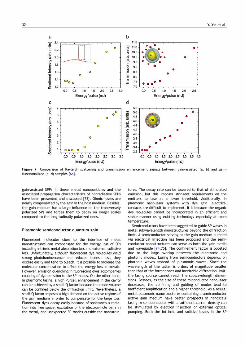
Luca et al. have prepared a gain-functionalized metalplasmonic nanostructure [64]. The smart gain-functionalizedcomposite is different from conventional gain-assistedsystems in which metal absorption losses remain unresolved.Instead of randomly dispersing fluorescent guest moleculesin a solution with metal nanoparticles, dye molecules areencapsulated into shells. The built-in gain elements in-tended for compensating internal losses are obtained byincorporating the optically active gain component ofRhodamine 6G dye molecules into the silica shell surround-ing the metal nanoparticles. The nonradiative excitationenergy transfer from the fluorescent dye molecules to SPresonance has been demonstrated. A comparison of themodified Rayleigh scattering and transmission as a functionof pumping energy between the gain-assisted and gain-functionalized plasmonic nanostructures is shown in Fig. 7.The results provide experimental proof that gain media,which are properly inserted into metal plasmonic nanos-tructures functionalize the gain unit for strongly absorbingmetals.
Near-field strong interactions between neighboring plas-monic particles provide highly enhanced localized EM fieldand excellent subwavelength energy confinement. This is apotential way to concentrate the energy. However, energydamping along the SPP propagating path due to metalabsorption can reduce the propagation length. Therefore,SPPs propagation with good confinement as well as smallenergy loss is necessary in order to produce subwavelengthplasmonic waveguides integrated with metal nanoparticlearrays [65–70]. It has been demonstrated that a gain mediumin metal nanoparticle arrays can enhance the propagationlength of the SPP and reduce the energy loss [71–73]. Citrintheoretically studied the benefits of embedding optical gainmedia in nanoparticle chains to offset the energy loss [72]. Inthe presence of a gain medium, exponential increase in theplasmon modes can compensate for nonradiative damping ofthe SP resonance decay. The dispersion equation governing
Figure 6 (a) Au and Ag nanorods used for the plasmonpropagation experiments; (b) optical microscope image of a4.7 mm long Au rod exposed to the illumination at 532 nmwith accordingly strong scattering at the rod input and theabsence of scattering at distal tip. (c) Same Au rod underillumination at 820 nm, and both ends of the rod exhibit strongemission/scattering; (d) and (e) a 4.7 mm long Ag rodilluminated at 532 and 820 nm, respectively; (f) a bimetalAu/Ag rod. The upper 40% of the rod is Au while the remainderis composed of Ag; (g) the Au end of the rod shown inpanel (f) under illumination at 820 nm; (h) Illumination atthe Ag tip by 820 nm with no emission from the Au tip isobservable [55].
Plasmonic nano-lasers 31
gain-assisted SPPs in linear metal nanoparticles and theassociated propagation characteristics of nonradiative SPPshave been presented and discussed [73]. Ohmic losses arenearly compensated by the gain in the host medium. Besides,the gain medium has a large influence on the transverselypolarized SPs and forces them to decay on longer scalescompared to the longitudinally polarized ones.
Plasmonic semiconductor quantum gain
Fluorescent molecules close to the interface of metalnanostructures can compensate for the energy loss of SPsincluding intrinsic metal absorption loss and external radiativeloss. Unfortunately, although fluorescent dye molecules yieldstrong photoluminescence and reduced intrinsic loss, theyoxidize easily and tend to bleach. It is possible to increase themolecular concentration to offset the energy loss in metals.However, emission quenching in fluorescent dyes accompaniescoupling of dye emission to the SP modes. On the other hand,in plasmonic lasing, a high Purcell enhancement in the cavitycan be achieved by a small Q factor because the mode volumecan be confined below the diffraction limit. Nevertheless, asmall Q factor imposes a high demand on the active regions ofthe gain medium in order to compensate for the large loss.Fluorescent dyes decay easily because of spontaneous radia-tion into free space, excitation of the electron–hole pairs inthe metal, and unexpected SP modes outside the nanostruc-
tures. The decay rate can be lowered to that of stimulatedemission, but this imposes stringent requirements on theemitters to lase at a lower threshold. Additionally, inplasmonic nano-laser systems with dye gain, electricalcontacts are difficult to implement. It is because the organicdye molecules cannot be incorporated in an efficient andstable manner using existing technology especially at roomtemperature.
Semiconductors have been suggested to guide SP waves inmetal subwavelength nanostructures beyond the diffractionlimit. A semiconductor serving as the gain medium pumpedvia electrical injection has been proposed and the semi-conductor nanostructures can serve as both the gain mediaand waveguide [74,75]. The confinement factor is boosteddue to the large overlap between the electronic andphotonic modes. Lasing from semiconductors depends onphotonic waves instead of plasmonic waves. Since thewavelength of the latter is orders of magnitude smallerthan that of the former ones and inevitable diffraction limit,the lasing source cannot reach the subwavelength dimen-sions. Besides, as the size of these miconductor nano-laserdecreases, the confining and guiding of modes lead toinefficient amplification and a higher threshold. As a result,metal plasmonic nanostructures containing a semiconductoractive gain medium have better prospects in nanoscalelasing. A semiconductor with a sufficient carrier density canbe stimulated by electron injection or external opticalpumping. Both the intrinsic and raditive losses in the SP
Figure 7 Comparison of Rayleigh scattering and transmission enhancement signals between gain-assisted (a, b) and gain-functionalized (c, d) samples [64].
Y. Yin et al.32
resonance can be mitigated and the localized EM modesincrease the performance of other nano-lasers.
Theoretically, some concepts and definitions have beenreexamined for novel plasmonic lasing devices with asemiconductor as the active gain medium. Li and Ningproposed the concept of a confinement factor for a metal–semiconductor–metal waveguide near SP resonance [76,77].The SPP modes exhibit an unexpected giant modal gain,which is thousands of times larger than the materials gain.Therefore, the large ratio of modal gain to materials gaincontributes to a large confinement factor. Hill et al. haveused a semiconductor core as the electrically pumped activegain medium and conducted metal encapsulation [78,79].The metal–insulator–metal waveguide is observed to reach1D mode confinement below the diffraction limit. Here, thecryogenic temperature required for lasing offsets the largeresistive loss from metal absorption. There is less Augerrecombination under cryogenic conditions and so a larger Qand lower threshold can be obtained.
Although wavelength compression of SP modes into thenanometer scale is attractive for nanoscale plasmonic lasingdevices, the effective minimum wavelength affects themetal absorption losses. Near the SP resonance frequency,the SP modes experience significant absorption losses whenpropagating along the metal interfaces [9,80]. To makethings more complicated, although SP resonance providessuperior localization, the small volume of the laser deviceforces the propagation of SPP to be highly confined in thevery small region of the metal interface further hinderingefficient gain compensation. When the emitting frequency ishigh, the carrier injection energy in the semiconductor goesin the positive direction but in the metal, it goes in theopposite direction. The opposite effects make the net gainalmost zero. Recently, Stockman analyzed full compensation(overcompensation) [81]. The instability of the transition toa lasing state further limits loss compensation.
Quantum treatment of SPs has been theoreticallyproposed to analyze the gain conditions and laser operationin plasmonic systems [82–84]. As an active gain mediumformed by the two-level emitters, the operating frequenciesof the semiconductor quantum structures can be modulatedto transfer energy into the desired spectral range. This isaccomplished by engineering the geometry of the metalplasmonic nanostructures. They also offer good quantumconfinement, large packing density, high transition effi-ciency, as well as narrow transition lines and the frequencyis tunable [85]. Stockman introduced a quantum generatorfor SPs by incorporating semiconductor quantum dots as theemitter and laser active medium and theoretically demon-strated the mechanism of spaser [7]. PbS QDs incorporatedinto polymer films adjacent to gold nanofilms have beenused as the amplifying medium to increase the propagationlength by 30% [86]. Semiconductor quantum wells have alsobeen widely used since current quantum well technology iscapable of compensating intrinsic SP attenuation even nearthe plasmon resonance and lengthening SPPs propagation.Ambati et al. investigated the emission phenomenon of anoptical emitter into various channels of SPs [87]. The activeplanar metal–film system comprises InGaN/GaN and a silverfilm and coupling between the SP modes and gain mediumcan be precisely controlled by strategically positioning theemitters.
Stimulated emission of plasmonic modes
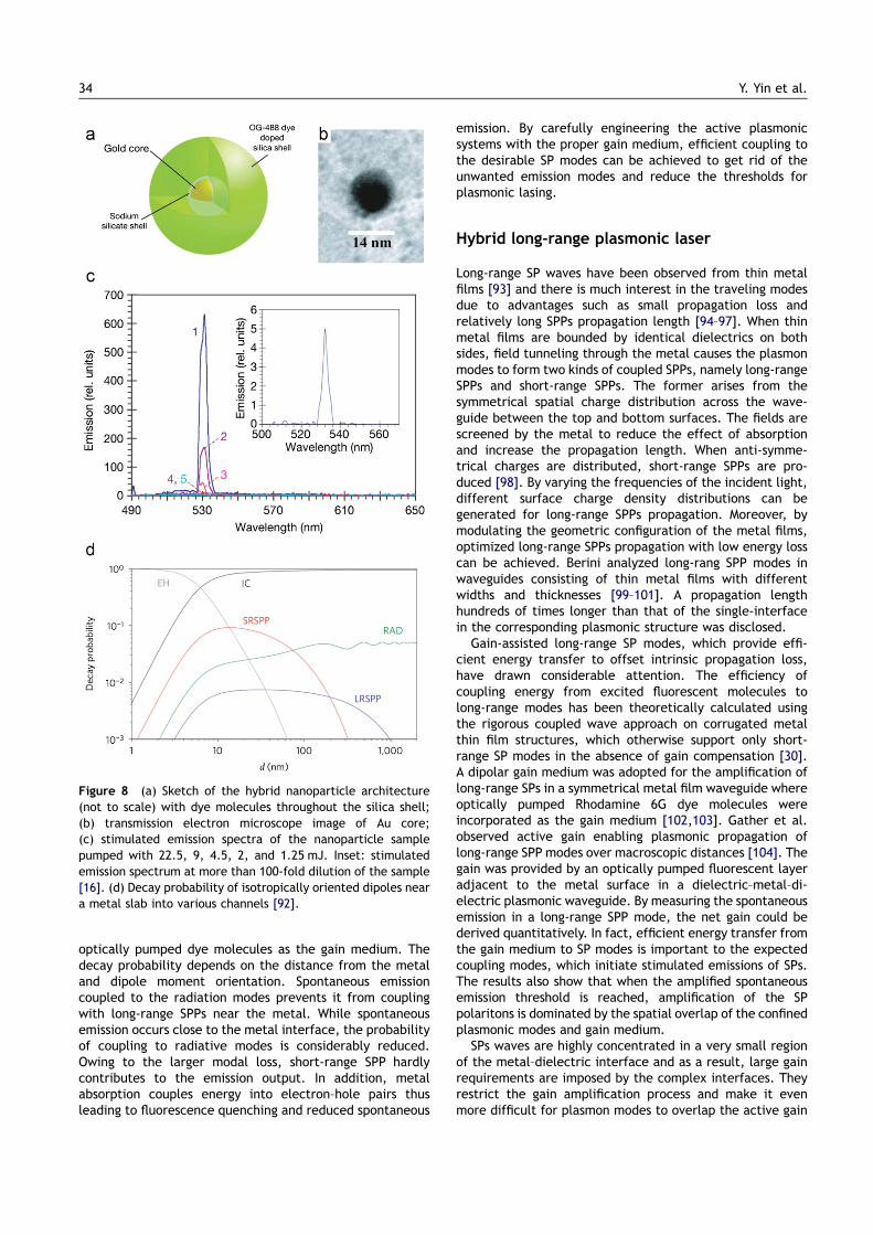
Although the well confined near-field of the SP modes maynot allow coupling to the far zone optical field, SPs canachieve amplification and radiation when combined with anactive molecule gain medium. This is because the moleculeis only affected by the field at the specific positionregardless of the overall symmetry of the entire local field.Seidel et al. observed stimulated emission of SPs at theinterface between a thin film and an optically pumped dyesolution [88]. Stimulated emission of SPs from dye-dopedpolymeric microcylinder cavities deposited on gold and silverwires was observed [89]. Noginov et al. added aggregatedsilver nanoparticles to a Rodamine 6G dye solution to enhancethe efficiency of spontaneous and stimulated emission [90].However, the feedback mechanism is still not well understood.Nanoparticles with a gold core and dye-doped silica shellwere employed to demonstrate resonant energy transferfrom excited molecules to SPs and stimulated emissionof SPs in the luminous mode [16]. The absorption loss oflocalized SPs in gold nanoparticles is sufficiently offset bythe active gain in the plasmonic nanosystem. Coupling of thestimulated emission of the SP modes to photonic modes at awavelength of 531 nm was experimentally confirmed andthe mechanism was studied. Fig. 8(a)–(c) depicts thestimulated emission spectra of the nanoparticle sample atdifferent energy pumping. When the pumping energy is low,emission is barely observed because there are no excitedgain molecules to transfer energy to the SP modes (spectra4 and 5). As the pumping energy is increased, emissionoccurs. If the pumping energy is increased to the criticalthreshold value, the stimulated emission of SP resonancebecomes intense. If the sample is diluted more than 100times, the emission intensity decreases but the spectralcharacteristics do not change. This demonstrates that thestimulated emission of SPs is produced by single nanopar-ticles, rather than collective stimulated emission effect in avolume of the gain medium.
Energy losses in the SP modes can be balanced byintroducing active gain media into the metal structures.Efficient coupling to the plasmon modes lowers the plasmonlasing threshold and aids in the formation of high-efficientcoherent radiation. Therefore, a good understanding of thefundamental interactions between SPPs and gain mediumenables wide applications on nanoscale plasmonic lasingsources [91]. Unfortunately, the process is rather complex.Efficient energy transfer from the gain medium to SP modescontributes to spontaneous emission which is important tothe expected coupling modes and initiation of stimulatedemissions of SPs. In the case when the pumping intensity isvery high, the competition between stimulated plasmonsemission and amplified spontaneous emission affects theSPPs propagation and undermine coupling to the plasmonicmodes. Therefore, amplified spontaneous emission of SPslimits the gain compensation for loss with regard to SPPpropagation. It is similar to that in a conventional laser.Recently, a new class of SPs amplifier benefiting from thereduced spontaneous emission may provide low-noiseoptical amplification and large loss compensation [92]. Manyenergy decay channels have been revealed based on thereduced spontaneous emission. Fig. 8(d) depicts the mainenergy decay channels for long-range SPPs amplication with
Plasmonic nano-lasers 33
optically pumped dye molecules as the gain medium. Thedecay probability depends on the distance from the metaland dipole moment orientation. Spontaneous emissioncoupled to the radiation modes prevents it from couplingwith long-range SPPs near the metal. While spontaneousemission occurs close to the metal interface, the probabilityof coupling to radiative modes is considerably reduced.Owing to the larger modal loss, short-range SPP hardlycontributes to the emission output. In addition, metalabsorption couples energy into electron–hole pairs thusleading to fluorescence quenching and reduced spontaneous
emission. By carefully engineering the active plasmonicsystems with the proper gain medium, efficient coupling tothe desirable SP modes can be achieved to get rid of theunwanted emission modes and reduce the thresholds forplasmonic lasing.
Hybrid long-range plasmonic laser
Long-range SP waves have been observed from thin metalfilms [93] and there is much interest in the traveling modesdue to advantages such as small propagation loss andrelatively long SPPs propagation length [94–97]. When thinmetal films are bounded by identical dielectrics on bothsides, field tunneling through the metal causes the plasmonmodes to form two kinds of coupled SPPs, namely long-rangeSPPs and short-range SPPs. The former arises from thesymmetrical spatial charge distribution across the wave-guide between the top and bottom surfaces. The fields arescreened by the metal to reduce the effect of absorptionand increase the propagation length. When anti-symme-trical charges are distributed, short-range SPPs are pro-duced [98]. By varying the frequencies of the incident light,different surface charge density distributions can begenerated for long-range SPPs propagation. Moreover, bymodulating the geometric configuration of the metal films,optimized long-range SPPs propagation with low energy losscan be achieved. Berini analyzed long-rang SPP modes inwaveguides consisting of thin metal films with differentwidths and thicknesses [99–101]. A propagation lengthhundreds of times longer than that of the single-interfacein the corresponding plasmonic structure was disclosed.
Gain-assisted long-range SP modes, which provide effi-cient energy transfer to offset intrinsic propagation loss,have drawn considerable attention. The efficiency ofcoupling energy from excited fluorescent molecules tolong-range modes has been theoretically calculated usingthe rigorous coupled wave approach on corrugated metalthin film structures, which otherwise support only short-range SP modes in the absence of gain compensation [30].A dipolar gain medium was adopted for the amplification oflong-range SPs in a symmetrical metal film waveguide whereoptically pumped Rhodamine 6G dye molecules wereincorporated as the gain medium [102,103]. Gather et al.observed active gain enabling plasmonic propagation oflong-range SPP modes over macroscopic distances [104]. Thegain was provided by an optically pumped fluorescent layeradjacent to the metal surface in a dielectric–metal–di-electric plasmonic waveguide. By measuring the spontaneousemission in a long-range SPP mode, the net gain could bederived quantitatively. In fact, efficient energy transfer fromthe gain medium to SP modes is important to the expectedcoupling modes, which initiate stimulated emissions of SPs.The results also show that when the amplified spontaneousemission threshold is reached, amplification of the SPpolaritons is dominated by the spatial overlap of the confinedplasmonic modes and gain medium.
SPs waves are highly concentrated in a very small regionof the metal–dielectric interface and as a result, large gainrequirements are imposed by the complex interfaces. Theyrestrict the gain amplification process and make it evenmore difficult for plasmon modes to overlap the active gain
Figure 8 (a) Sketch of the hybrid nanoparticle architecture(not to scale) with dye molecules throughout the silica shell;(b) transmission electron microscope image of Au core;(c) stimulated emission spectra of the nanoparticle samplepumped with 22.5, 9, 4.5, 2, and 1.25 mJ. Inset: stimulatedemission spectrum at more than 100-fold dilution of the sample[16]. (d) Decay probability of isotropically oriented dipoles neara metal slab into various channels [92].
Y. Yin et al.34
medium. Operation at frequencies much lower than the SPresonance frequency is widely adopted. One of advantagesis that the plasmon modes are not strongly confined to themetal surface and can therefore overlap with the active gainstructures [105–108]. Genov et al. demonstrated that bykeeping plasmon modes away from the resonance frequency,the light–matter interactions in the plasmonic systems canbe increased in two dimensions [109]. However, this doesnot bode well for localized confinement. Long-range SPPsexhibit optical confinement which is comparable to that ofconventional dielectric waveguides and so they cannotreach the subwavelength dimensions.
Tight confinement of the EM energy affects the energyloss in the coupled optical field on the metal side of theinterface. By reducing the spatial distribution of the SPPmodes in the nanostructures, good confinement can beattained, but it causes more metal absorption and energyloss. Nezhad et al. produced optically pumped metal–dielectric cavities comprising a metal bilayer surroundingan InGaAsP disk as gain medium [110]. By increasing thediameter of the gain disk, the optical mode was notobserved from the metal surface in addition to reducedresistive loss. Although the cavity size is smaller than theemission wavelength in all three dimensions, the diffractionlimit remains because of the nature of the photonic modesinstead of plasmonic ones.
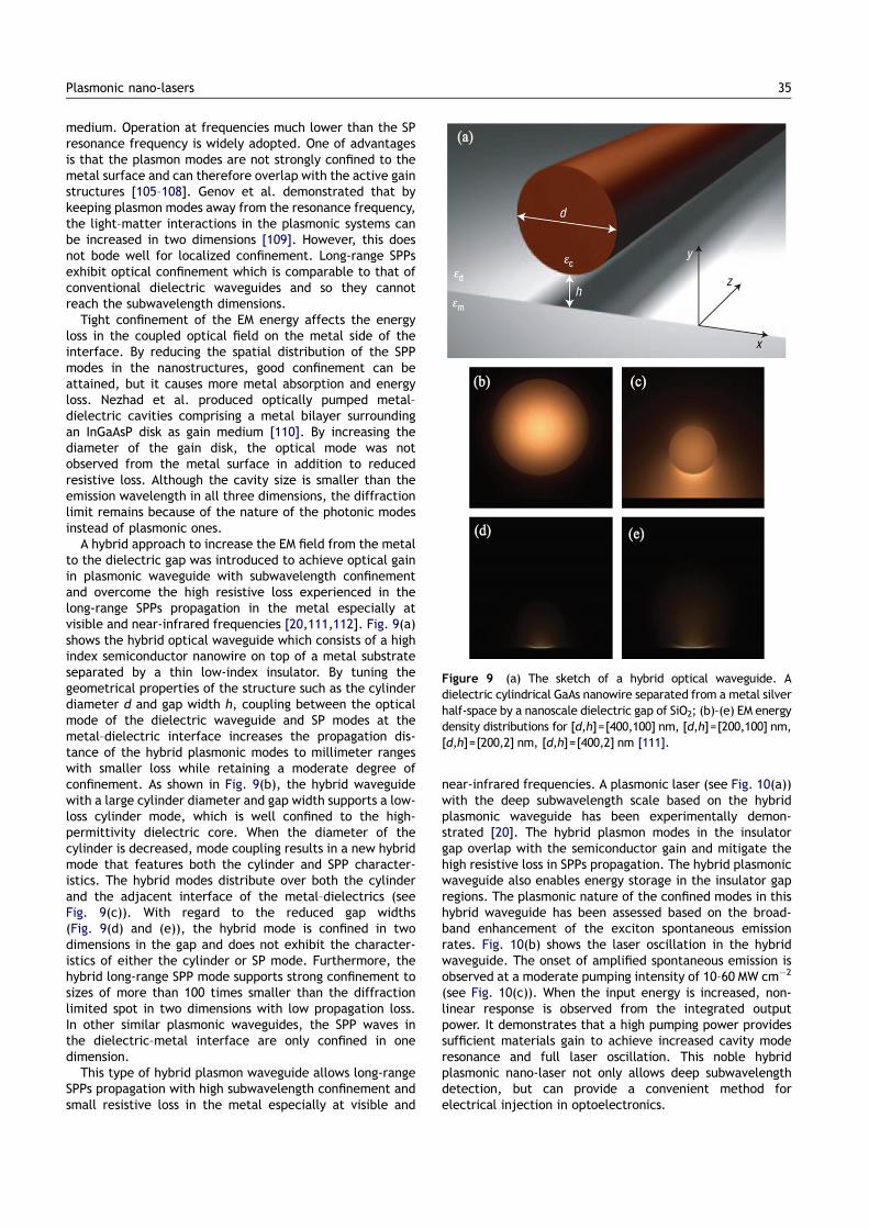
A hybrid approach to increase the EM field from the metalto the dielectric gap was introduced to achieve optical gainin plasmonic waveguide with subwavelength confinementand overcome the high resistive loss experienced in thelong-range SPPs propagation in the metal especially atvisible and near-infrared frequencies [20,111,112]. Fig. 9(a)shows the hybrid optical waveguide which consists of a highindex semiconductor nanowire on top of a metal substrateseparated by a thin low-index insulator. By tuning thegeometrical properties of the structure such as the cylinderdiameter d and gap width h, coupling between the opticalmode of the dielectric waveguide and SP modes at themetal–dielectric interface increases the propagation dis-tance of the hybrid plasmonic modes to millimeter rangeswith smaller loss while retaining a moderate degree ofconfinement. As shown in Fig. 9(b), the hybrid waveguidewith a large cylinder diameter and gap width supports a low-loss cylinder mode, which is well confined to the high-permittivity dielectric core. When the diameter of thecylinder is decreased, mode coupling results in a new hybridmode that features both the cylinder and SPP character-istics. The hybrid modes distribute over both the cylinderand the adjacent interface of the metal–dielectrics (seeFig. 9(c)). With regard to the reduced gap widths(Fig. 9(d) and (e)), the hybrid mode is confined in twodimensions in the gap and does not exhibit the character-istics of either the cylinder or SP mode. Furthermore, thehybrid long-range SPP mode supports strong confinement tosizes of more than 100 times smaller than the diffractionlimited spot in two dimensions with low propagation loss.In other similar plasmonic waveguides, the SPP waves inthe dielectric–metal interface are only confined in onedimension.
This type of hybrid plasmon waveguide allows long-rangeSPPs propagation with high subwavelength confinement andsmall resistive loss in the metal especially at visible and
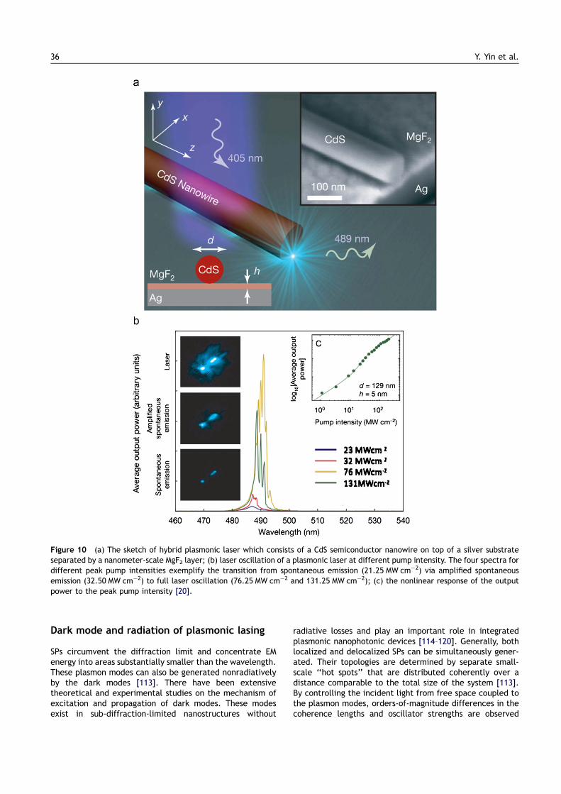
near-infrared frequencies. A plasmonic laser (see Fig. 10(a))with the deep subwavelength scale based on the hybridplasmonic waveguide has been experimentally demon-strated [20]. The hybrid plasmon modes in the insulatorgap overlap with the semiconductor gain and mitigate thehigh resistive loss in SPPs propagation. The hybrid plasmonicwaveguide also enables energy storage in the insulator gapregions. The plasmonic nature of the confined modes in thishybrid waveguide has been assessed based on the broad-band enhancement of the exciton spontaneous emissionrates. Fig. 10(b) shows the laser oscillation in the hybridwaveguide. The onset of amplified spontaneous emission isobserved at a moderate pumping intensity of 10–60 MW cm�2
(see Fig. 10(c)). When the input energy is increased, non-linear response is observed from the integrated outputpower. It demonstrates that a high pumping power providessufficient materials gain to achieve increased cavity moderesonance and full laser oscillation. This noble hybridplasmonic nano-laser not only allows deep subwavelengthdetection, but can provide a convenient method forelectrical injection in optoelectronics.
Figure 9 (a) The sketch of a hybrid optical waveguide. Adielectric cylindrical GaAs nanowire separated from a metal silverhalf-space by a nanoscale dielectric gap of SiO2; (b)–(e) EM energydensity distributions for [d,h]=[400,100] nm, [d,h]=[200,100] nm,[d,h]=[200,2] nm, [d,h]=[400,2] nm [111].
Plasmonic nano-lasers 35
Dark mode and radiation of plasmonic lasing
SPs circumvent the diffraction limit and concentrate EMenergy into areas substantially smaller than the wavelength.These plasmon modes can also be generated nonradiativelyby the dark modes [113]. There have been extensivetheoretical and experimental studies on the mechanism ofexcitation and propagation of dark modes. These modesexist in sub-diffraction-limited nanostructures without
radiative losses and play an important role in integratedplasmonic nanophotonic devices [114–120]. Generally, bothlocalized and delocalized SPs can be simultaneously gener-ated. Their topologies are determined by separate small-scale ‘‘hot spots’’ that are distributed coherently over adistance comparable to the total size of the system [113].By controlling the incident light from free space coupled tothe plasmon modes, orders-of-magnitude differences in thecoherence lengths and oscillator strengths are observed
Figure 10 (a) The sketch of hybrid plasmonic laser which consists of a CdS semiconductor nanowire on top of a silver substrateseparated by a nanometer-scale MgF2 layer; (b) laser oscillation of a plasmonic laser at different pump intensity. The four spectra fordifferent peak pump intensities exemplify the transition from spontaneous emission (21.25 MW cm�2) via amplified spontaneousemission (32.50 MW cm�2) to full laser oscillation (76.25 MW cm�2 and 131.25 MW cm�2); (c) the nonlinear response of the outputpower to the peak pump intensity [20].
Y. Yin et al.36
from one mode to another at nearby frequencies. Thiscreates the radiative mode and dark mode. Because ofradiation coupled to the external forces, the radiative modehas a large scattering cross section and small Q factor. Incomparison, the dark mode avoids radiation and interfer-ence from the outside. Therefore, dark modes always leadto a relatively large factor. Selection of dark eigenmodes forplasmonic lasing has been theoretically shown [7]. The sizeof the gain medium can be moderated to tune the transitionfrequency. At a given frequency, an eigenmode is selectedby positioning the gain dots in the region where it local fieldsare maximum. The degree of localization of the dark orluminous eigenmodes in different energy transitions has alsobeen illustrated.
Dark plasmon modes cannot be excited or observed fromthe far-field zone. They only exist in well confined near-fieldwithout coupling to the far zone optical field. Therefore, inthe cavity of a plasmonic laser, the dark modes propagatealong the metal–dielectrics interfaces without radiativeloss and so the stimulated emission of SPs is amplified. Theincreased SP population benefits from the dark modeswithout radiation. It resembles an optical cavity with tworeflectors with a reflectance at 100% allowing light tobounce back and forth when it passes through the gainmedium. Consequently, a high Q factor and low thresholdcan be achieved.
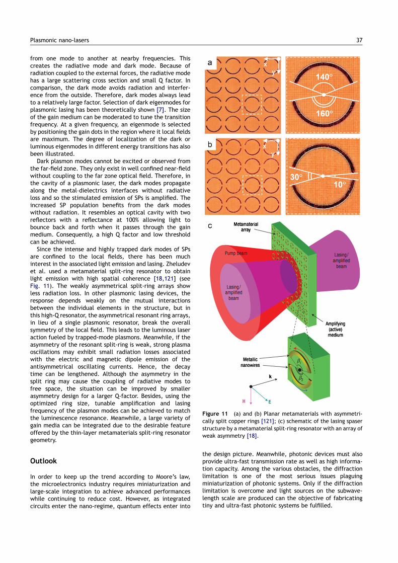
Since the intense and highly trapped dark modes of SPsare confined to the local fields, there has been muchinterest in the associated light emission and lasing. Zheludevet al. used a metamaterial split-ring resonator to obtainlight emission with high spatial coherence [18,121] (seeFig. 11). The weakly asymmetrical split-ring arrays showless radiation loss. In other plasmonic lasing devices, theresponse depends weakly on the mutual interactionsbetween the individual elements in the structure, but inthis high-Q resonator, the asymmetrical resonant ring arrays,in lieu of a single plasmonic resonator, break the overallsymmetry of the local field. This leads to the luminous laseraction fueled by trapped-mode plasmons. Meanwhile, if theasymmetry of the resonant split-ring is weak, strong plasmaoscillations may exhibit small radiation losses associatedwith the electric and magnetic dipole emission of theantisymmetrical oscillating currents. Hence, the decaytime can be lengthened. Although the asymmetry in thesplit ring may cause the coupling of radiative modes tofree space, the situation can be improved by smallerasymmetry design for a larger Q-factor. Besides, using theoptimized ring size, tunable amplification and lasingfrequency of the plasmon modes can be achieved to matchthe luminescence resonance. Meanwhile, a large variety ofgain media can be integrated due to the desirable featureoffered by the thin-layer metamaterials split-ring resonatorgeometry.
Outlook
In order to keep up the trend according to Moore’s law,the microelectronics industry requires miniaturization andlarge-scale integration to achieve advanced performanceswhile continuing to reduce cost. However, as integratedcircuits enter the nano-regime, quantum effects enter into
the design picture. Meanwhile, photonic devices must alsoprovide ultra-fast transmission rate as well as high informa-tion capacity. Among the various obstacles, the diffractionlimitation is one of the most serious issues plaguingminiaturization of photonic systems. Only if the diffractionlimitation is overcome and light sources on the subwave-length scale are produced can the objective of fabricatingtiny and ultra-fast photonic systems be fulfilled.
Figure 11 (a) and (b) Planar metamaterials with asymmetri-cally split copper rings [121]; (c) schematic of the lasing spaserstructure by a metamaterial split-ring resonator with an array ofweak asymmetry [18].
Plasmonic nano-lasers 37
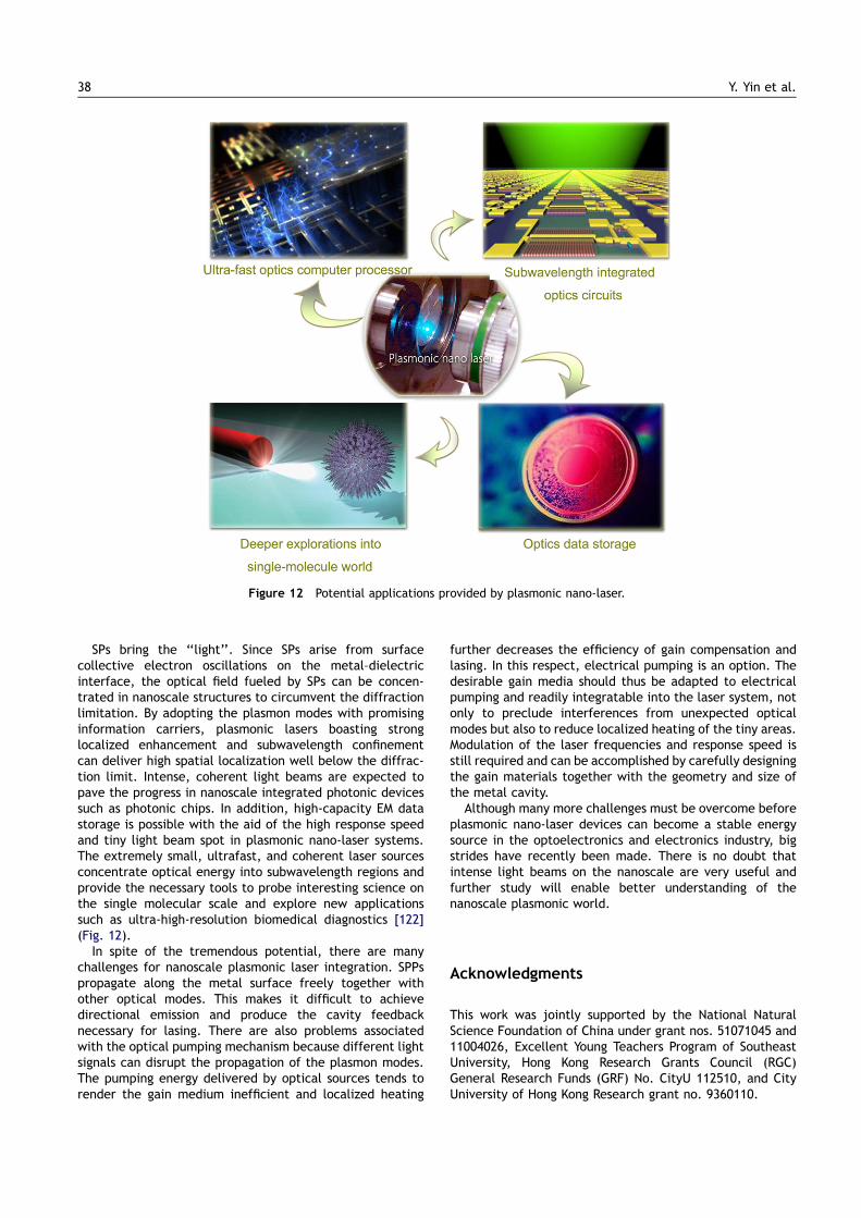
SPs bring the ‘‘light’’. Since SPs arise from surfacecollective electron oscillations on the metal–dielectricinterface, the optical field fueled by SPs can be concen-trated in nanoscale structures to circumvent the diffractionlimitation. By adopting the plasmon modes with promisinginformation carriers, plasmonic lasers boasting stronglocalized enhancement and subwavelength confinementcan deliver high spatial localization well below the diffrac-tion limit. Intense, coherent light beams are expected topave the progress in nanoscale integrated photonic devicessuch as photonic chips. In addition, high-capacity EM datastorage is possible with the aid of the high response speedand tiny light beam spot in plasmonic nano-laser systems.The extremely small, ultrafast, and coherent laser sourcesconcentrate optical energy into subwavelength regions andprovide the necessary tools to probe interesting science onthe single molecular scale and explore new applicationssuch as ultra-high-resolution biomedical diagnostics [122](Fig. 12).
In spite of the tremendous potential, there are manychallenges for nanoscale plasmonic laser integration. SPPspropagate along the metal surface freely together withother optical modes. This makes it difficult to achievedirectional emission and produce the cavity feedbacknecessary for lasing. There are also problems associatedwith the optical pumping mechanism because different lightsignals can disrupt the propagation of the plasmon modes.The pumping energy delivered by optical sources tends torender the gain medium inefficient and localized heating
further decreases the efficiency of gain compensation andlasing. In this respect, electrical pumping is an option. Thedesirable gain media should thus be adapted to electricalpumping and readily integratable into the laser system, notonly to preclude interferences from unexpected opticalmodes but also to reduce localized heating of the tiny areas.Modulation of the laser frequencies and response speed isstill required and can be accomplished by carefully designingthe gain materials together with the geometry and size ofthe metal cavity.
Although many more challenges must be overcome beforeplasmonic nano-laser devices can become a stable energysource in the optoelectronics and electronics industry, bigstrides have recently been made. There is no doubt thatintense light beams on the nanoscale are very useful andfurther study will enable better understanding of thenanoscale plasmonic world.
Acknowledgments
This work was jointly supported by the National NaturalScience Foundation of China under grant nos. 51071045 and11004026, Excellent Young Teachers Program of SoutheastUniversity, Hong Kong Research Grants Council (RGC)General Research Funds (GRF) No. CityU 112510, and CityUniversity of Hong Kong Research grant no. 9360110.
Figure 12 Potential applications provided by plasmonic nano-laser.
Y. Yin et al.38
References
[1] A.L. Schawlow, C.H. Townes, Phys. Rev. 112 (1958)1940–1949.
[2] M. Fujihira, H. Monobe, N. Yamamoto, H. Muramatsu,N. Chiba, K. Nakajima, T. Ataka, Ultramicroscopy 61 (1995)271–277.
[3] L. Novotny, E.J. Sanchez, X.S. Xie, Ultramicroscopy 71 (1998)21–29.
[4] P.F. Barbara, D.M. Adams, D.B. O’Connor, Annu. Rev. Mater.Sci. 29 (1999) 433–469.
[5] E.J. Sanchez, L. Novotny, X.S. Xie, Phys. Rev. Lett. 82 (1999)4014–4017.
[6] H.G. Park, S.H. Kim, S.H. Kwon, Y.G. Ju, J.K. Yang, J.H. Baek,S.B. Kim, Y.H. Lee, Science 305 (2004) 1444–1447.
[7] D.J. Bergman, M.I. Stockman, Phys. Rev. Lett. 90 (2003)027402.
[8] H. Raether, Surface Plasmons on Smooth and Rough Surfacesand on Gratings, Springer, Berlin, 1988.
[9] E. Ozbay, Science 311 (2006) 189–193.[10] J.A. Conway, S. Sahni, T. Szkopek, Opt. Express 15 (2007)
4474–4484.[11] M.L. Brongersma, V.M. Shalaev, Science 328 (2010) 440–441.[12] A.V. Krasavin, A.V. Zayats, Opt. Express 18 (2010)
11791–11799.[13] M.I. Stockman, Phys. Rev. Lett. 93 (2004) 137404.[14] M.I. Stockman, J. Opt. 12 (2010) 024004.[15] J.A. Gordon, R.W. Ziolkowski, Opt. Express 15 (2007)
2622–2653.[16] M.A. Noginov, G. Zhu, A.M. Belgrave, R. Bakker, V.M. Shalaev,
E.E. Narimanov, S. Stout, E. Herz, T. Suteewong, U. Wiesner,Nat. Mater. 460 (2009) 1110–1113.
[17] M.I. Stockman, Nat. Photonics 2 (2008) 327–329.[18] N.I. Zheludev, S.L. Prosvirnin, N. PapasimakiS, V.A. Fedotov,
Nat. Photonics 2 (2008) 351–354.[19] E.M. Purcell, Phys. Rev. 69 (1946) 681.[20] R.F. Oulton, V.J. Sorger, T. Zentgraf, R.M. Ma, C. Gladden,
L. Dai, G. Bartal, X. Zhang, Nature 461 (2009) 629–632.[21] K. Nozaki, S. Kita, T. Baba, Opt. Express 15 (2007) 7506–7514.[22] A. Hatice, E. Dirk, V. Jelena, Nat. Phys. 2 (2006) 484–488.[23] H. Ditlbacher, A. Hohenau, D. Wagner, U. Kreibig, M. Rogers,
F. Hofer, F.R. Aussenegg, J.R. Krenn, Phys. Rev. Lett. 95(2005) 257403.
[24] J. Schoenwald, E. Burstein, J.M. Elson, Solid State Commun.12 (1973) 185–189.
[25] B. Lamprecht, J.R. Krenn, G. Schider, H. Ditlbacher, M. Salerno,N. Felidj, A. Leitner, F.R. Aussenegg, J.C. Weeber, Appl. Phys.Lett. 79 (2001) 51–53.
[26] J.C. Weeber, J.R. Krenn, A. Dereux, B. Lamprecht,Y. Lacroute, J.P. Goudonnet, Phys. Rev. B 64 (2001) 045411.
[27] T. Okamoto, F. H’Dhili, S. Kawata, Appl. Phys. Lett. 85 (2004)3968–3970.
[28] C. Marquart, S.I. Bozhevolnyi, K. Leosson, Opt. Express13 (2005) 3303–3309.
[29] T. Okamoto, J. Simonen, S. Kawata, Phys. Rev. B 77 (2008)115425.
[30] T. Okamoto, J. Simonen, S. Kawata, Opt. Express 17 (2009)8294–8301.
[31] I.R. Hooper, J.R. Sambles, Phys. Rev. B 65 (2002) 165432.[32] I.R. Hooper, J.R. Sambles, Phys. Rev. B 66 (2002) 205408.[33] D. Gerard, L. Salomon, F. de Fornel, Phys. Rev. B 69 (2004)
113405.[34] I.R. Hooper, J.R. Sambles, Phys. Rev. B 70 (2004) 045421.[35] B. Wang, L. Aigouy, E. Bourhis, J. Gierak, J.P. Hugonin,
P. Lalanne, Appl. Phys. Lett. 94 (2009) 011114.[36] K. Sakoda, Opt. Express 4 (1999) 167–176.
[37] U. Kreibig, M. Vollmer, Optical Properties of Metal Clusters,Springer, Heidelberg, 1995.
[38] M.D. Malinsky, K. Lance Kelly, G.C. Schatz, R.P. Van Duyne,J. Am. Chem. Soc. 123 (2001) 1471–1482.
[39] T. Qiu, X.L. Wu, Y.C. Cheng, G.G. Siu, P.K. Chu, Appl. Phys.Lett. 88 (2006) 143111.
[40] T. Qiu, X.L. Wu, J.C. Shen, P.K. Chu, Appl. Phys. Lett. 89(2006) 131914.
[41] M. Quinten, A. Leitner, J.R. Krenn, F.R. Aussenegg, Opt. Lett.23 (1998) 1331–1333.
[42] M.L. Brongersma, J.W. Hartman, H.A. Atwater, Phys. Rev. B62 (2000) 16356–16359.
[43] K.H. Su, Q.H. Wei, X. Zhang, Nano Lett. 3 (2003) 1087–1090.[44] Q.H. Wei, K.H. Su, S. Durant, X. Zhang, Nano Lett. 4 (2004)
1067–1071.[45] W.H. Weber, G.W. Ford, Phys. Lett. B 70 (2004) 125429.[46] D.S. Citrin, Nano Lett. 4 (2004) 1561–1565.[47] S.G. Zou, G.C. Schatz, Phys. Rev. B 74 (2006) 125111.[48] A.O. Pinchuk, G.C. Schatz, Mater. Sci. Eng., B 149 (2007)
251–258.[49] V.A. Markel, A.K. Sarychev, Phys. Rev. B 75 (2007) 085426.[50] S.A. Maier, P.G. Kik, H.A. Atwater, Appl. Phys. Lett. 81 (2002)
1714–1716.[51] S.A. Maier, P.G. Kik, H.A. Atwater, S. Meltzer, E. Harel,
B.E. Koel, A.A.G. Requicha, Nat. Mater. 2 (2003) 229–232.[52] J.R. Krenn, J.C. Weeber, A. Dereux, E. Bourillot,
J.P. Goudonnet, Phys. Rev. B 60 (1999) 5029–5033.[53] A.M. Funston, C. Novo, T.J. Davis, P. Mulvaney, Nano Lett. 9
(2009) 1651–1658.[54] J.C. Weeber, A. Dereux, Phys. Rev. B 60 (1999) 9061–9068.[55] R.M. Dickson, L.A. Lyon, J. Phys. Chem. B 104 (2000)
6095–6098.[56] N.M. Lawandy, Appl. Phys. Lett. 85 (2004) 5040–5042.[57] N.M. Lawandy, Appl. Phys. Lett. 95 (2009) 234101.[58] M.A. Noginov, G. Zhu, M. Bahoura, J. Adegoke, C.E. Small,
B.A. Ritzo, V.P. Drachev, V.M. Shalaev, Opt. Lett. 31 (2006)3022–3024.
[59] M.A. Noginov, G. Zhu, M. Bahoura, J. Adegoke, C. Small,B.A. Ritzo, V.P. Drachev, V.M. Shalaev, Appl. Phys. B 86 (2007)455–460.
[60] R.R. Chance, A. Prock, R. Silbey, Adv. Chem. Phys. 37 (1978)1–65.
[61] W.H. Weber, C.F. Eagen, Opt. Lett. 4 (1979) 236–238.[62] J. Gersten, A. Nitzan, J. Chem. Phys. 75 (1981) 1139–1152.[63] T. Qiu, F. Kong, X.Q. Yu, W.J. Zhang, X.Z. Lang, P.K. Chu,
Appl. Phys. Lett. 95 (2009) 213104.[64] A. De Luca, M.P. Grzelczak, I. Pastoriza-Santos, L.M. Liz-
Marzan, M. La Deda, M. Striccoli, G. Strangi, ACS Nano5 (2011) 5823–5829.
[65] M. Conforti, M. Guasoni, J. Opt. Soc. Am. B 27 (2010)1576–1582.
[66] A. Al �u, N. Engheta, Phys. Rev. B 74 (2006) 205436.[67] A.F. Koenderink, A. Polman, Phys. Rev. B 74 (2006) 033402.[68] C.R. Simovski, A.J. Viitanen, S.A. Tretyakov, Phys. Rev. E
72 (2005) 066606.[69] R.A. Shore, A.D. Yaghjian, Electron. Lett. 41 (2005) 578–580.[70] S.A. Maier, P.G. Kik, H.A. Atwater, Phys. Rev. B 67 (2003)
205402.[71] A.V. Maslov, C.Z. Ning, IEEE J. Quantum Electron. 40 (2004)
1389–1397.[72] D.S. Citrin, Opt. Express 31 (2006) 98–100.[73] I.B. Udagedara, I.D. Rukhlenko, M. Premaratne, Phys. Rev. B
83 (2011) 115451.[74] A.V. Maslov, C.Z. Ning, Appl. Phys. Lett. 83 (2003) 1237–1239.[75] A.V. Maslov, C.Z. Ning, Opt. Lett. 29 (2004) 572–574.[76] D.B. Li, C.Z. Ning, Phys. Rev. B 80 (2009) 153304.[77] D.B. Li, C.Z. Ning, Appl. Phys. Lett. 96 (2010) 181109.
Plasmonic nano-lasers 39
[78] M.T. Hill, M. Marell, E.S.P. Leong, B. Smalbrugge, Y.C. Zhu,M.H. Sun, P.J. van Veldhoven, E.J. Geluk, F. Karouta, Y.S. Oei,R. Notzel, C.Z. Ning, M.K. Smit, Opt. Express (2003)11107–11112.
[79] M.T. Hill, Y.S. Oei, B. Smalbrugge, Y.C. Zhu, T. de Vries, P.J. vanVeldhoven, F.W.M. van Otten, T.J. Eijkemans, J.P. Turkiewicz,H. de Waardt, E.J. Geluk, S.H. Kwon, Y.H. Lee, R. Notzel,M.K. Smit, Nat. Photonics 1 (2007) 589–594.
[80] W.L. Barnes, A. Dereux, T.W. Ebbesen, Nature 424 (2003)824–830.
[81] M.I. Stockman, Phys. Rev. Lett. 106 (2011) 156802.[82] D.E. Chang, A.S. Sorensen, P.R. Hemmer, M.D. Lukin, Phys.
Rev. Lett. 97 (2006) 053002.[83] Y.Y. Gong, J. Vuckovic, Appl. Phys. Lett. 90 (2007) 033113.[84] A. Archambault, F. Marquier, J.J. Greffet, Phys. Rev. B
82 (2010) 035411.[85] V.I. Klimov, A.A. Mikhailovsky, S. Xu, A. Malko, J.A. Hollingsworth,
C.A. Leatherdale, H.J. Eisler, M.G. Bawendi, Science 290 (2000)314–317.
[86] P.M. Bolger, W. Dickson, A.V. Krasavin, L. Liebscher, S.G. Hickey,D.V. Skryabin, A.V. Zayats (Eds.), Opt. Lett., 35, 2010,pp. 1197–1199.
[87] M. Ambati, D.A. Genov, R.F. Oulton, X. Zhang, IEEE J. Sel.Top. Quantum Electron. 14 (2008) 1395–1403.
[88] J. Seidel, S. Grafstrom, L. Eng, Phys. Rev. Lett. 94 (2005)177401.
[89] J.K. Kitur, V.A. Podolskiy, M.A. Noginov, Phys. Rev. Lett. 106(2011) 183903.
[90] M.A. Noginov, G. Zhu, M. Bahoura, C.E. Small, C. Davison,J. Adegoke, Phys. Rev. B 74 (2006) 184203.
[91] Y.H. Chen, J.F. Li, M.L. Ren, B.L. Wang, J.X. Fu, S.Y. Liu,Z.Y. Li, Appl. Phys. Lett. 98 (2011) 261912.
[92] I. De Leon, P. Berini, Nat. Photonics 4 (2011) 382–387.[93] D. Sarid, Phys. Rev. Lett. 47 (1981) 1927–1930.[94] G.I. Stegeman, J.J. Burke, D.G. Hall, Appl. Phys. Lett. 41
(1982) 906–908.[95] T. Inagaki, M. Motosuga, E.T. Arakawa, J.P. Goudonnet, Phys.
Rev. B 32 (1985) 6238–6345.[96] R.K. Hickernell, D. Sarid, J. Opt. Soc. Am. B 3 (1986)
1059–1069.[97] S.D. Gupta, G.V. Varada, G.S. Agarwal, Phys. Rev. B 36 (1987)
6331–6635.[98] G. Winter, S. Wedge, W.L. Barnes, New J. Phys. 8 (2006) 125.[99] P. Berini, Phys. Rev. B 61 (2000) 10484–10503.
[100] P. Berini, J. Appl. Phys. 98 (2005) 043109.[101] P. Berini, C. Robert, L. Nancy, IEEE J. Sel. Top. Quantum
Electron. 14 (2008) 1479–1495.[102] I. De Leon, P. Berini, Phys. Rev. B 78 (2008) 161401.[103] I. De Leon, P. Berini, Opt. Express 17 (2009) 20191–20202.[104] M.C. Gather, K. Meerholz, N. Danz, K. Leosso, Nat. Photonics
4 (2010) 457–461.[105] K. Unterrainer, R. Colombelli, C. Gmach, F. Capasso,
H.Y. Hwang, A.M. Sergent, D.L. Sivco, A.Y. Cho, Appl. Phys.Lett. 80 (2002) 3060–3062.
[106] B.S. Williams, S. Kumar, H. Callebaut, Q. Hu, J.L. Reno, Appl.Phys. Lett. 83 (2003) 2124–2126.
[107] J.A. Fan, M.A. Belkin, F. Capasso, S. Khanna, M. Lachab,A.G. Davies, E.H. Linfield, Opt. Express 14 (2006) 11672–11680.
[108] C. Manolatou, F. Rana, IEEE J. Quantum Electron. 44 (2008)435–447.
[109] D.A. Genov, R.F. Oulton, G. Barta, X. Zhang, Phys. Rev. B83 (2011) 245312.
[110] M.P. Nezhad, A. Simic, O. Bondarenko, B. Slutsky, A. Mizrahi,L. Feng, V. Lomakin, Y. Fainman, Nat. Photonics 4 (2010) 395–399.
[111] R.F. Oulton, V.J. Sorger, D.A. Genov, D.F.P. Pile, X. Zhang, Nat.Photonics 2 (2008) 496–500.
[112] V.J. Sorger, Z.L. Ye, R.F. Oulton, Y. Wang, G. Bartal, X.B. Yin,X. Zhang, Nature Commun. 2 (2011) 331.
[113] M.I. Stockman, S.V. Faleev, D.J. Bergman, Phys. Rev. Lett.87 (2001) 167401.
[114] S. Zhang, D.A. Genov, Y. Wang, M. Liu, X. Zhang, Phys. Rev.Lett. 101 (2008) 047401.
[115] M.Z. Liu, T.W. Lee, S.K. Gray, P.G. Sionnest, M. Pelton, Phys.Rev. Lett. 102 (2009) 107401.
[116] A.L. Koh, K. Bao, I. Khan, W.E. Smith, G. Kothleitner,P. Nordlander, S.A. Maier, D.W. McComb, ACS Nano 3 (2009)3015–3022.
[117] M.W. Chu, V. Myroshnychenko, C.H. Chen, J.P. Deng, C.Y. Mou,F.J. Garcia de Abajo, Nano Lett. 9 (2009) 399–404.
[118] V. Klimov, G.Y. Guo, J. Phys. Chem. C 114 (2010) 22398–22405.[119] Z.G. Dong, H. Liu, M.X. Xu, T. Li, S.M. Wang, J.X. Cao,
S.N. Zhu, X. Zhang, Opt. Express 18 (2010) 22413–22417.[120] C.G Biris, N.C. Panoiu, Nanotechnology 22 (2011) 235502.[121] V.A. Fedotov, M. Rose, S.L. Prosvirnin, N. Papasimakis,
N.I. Zheludev, Phys. Rev. Lett. 99 (2007) 147401.[122] V.J. Sorger, X. Zhang, Science 333 (2011) 709–710.
Yin Yin received his BS degree in physicsfrom Southeast University, China in 2009. Heis currently a PhD candidate in the Depart-ment of Physics, Southeast University. Hismain research interests are metamaterialsand plasmonics as well as their applicationsto nano-laser and optofluidic systems.
Teng Qiu received his BS in chemistry fromNanjing University, China in 2002 and PhD incondensed matter physics from NanjingUniversity in 2007. From 2004 to 2008, hewas affiliated with Prof. Paul K. Chu’sresearch group in City University of HongKong. He is currently a full professor ofphysics at Southeast University, China. In2010, he was an Alexander von Humboldtfellow in the Leibniz Institute for Solid State
and Materials Research in Dresden, Germany. His current researchfocuses on surface-enhanced spectroscopy. He has authored andco-authored about 60 refereed journal publications.
Jiaqi Li received his PhD degree in 2008from Nanjing University. In 2009–2010, heworked as a research fellow in NanyangTechnological University, Singapore. He iscurrently a lecturer in the Physics Depart-ment of Southeast University and his re-search interests are nano-photonics andplasmonics.
Paul K. Chu received his BS in mathematicsfrom The Ohio State University in 1977 and MSand PhD in chemistry from Cornell Universityin 1979 and 1982, respectively. He is the ChairProfessor of Materials Engineering in theDepartment of Physics & Materials Science inCity University of Hong Kong and holdsadvisory or visiting professorships in 13 uni-versities and research institutes in China.Paul’s research activities are quite diverse
encompassing plasma science and engineering, surface engineering,and various types of materials and nanotechnology. Paul is the
Y. Yin et al.40

co-editor of seven books on plasma science, biomedical engineering,and nanotechnology. He has co-authored more than 20 book chaptersas well as 900 journal papers. He has also given more than 100 invitedlectures and talks. He has been granted 11 US patents, 7 Chinesepatents, and 1 European patent and founded 3 companies. He is thechairman of the Plasma-Based Ion Implantation (PBII&D) InternationalCommittee and a member of the Ion Implantation Technology (IIT)International Committee and IEEE Nuclear and Plasma Science Society(NPSS) Fellow Evaluation Committee. He is Fellow of the American
Physical Society (APS), American Vacuum Society (AVS), Institute ofElectrical and Electronics Engineers (IEEE), and Hong Kong Institutionof Engineers (HKIE). He is the senior editor of IEEE Transactions onPlasma Science, associate editor of Materials Science & EngineeringReports, and editorial board member of 7 journals, includingBiomaterials. He has won a number of awards, including the 2007IEEE NPSS Merit Award and Materials Research Society (Taiwan) JWMayer Lectureship. He was the general chair of the 3rd IEEEInternational NanoElectronics Conference in Hong Kong in 2010.
Plasmonic nano-lasers 41


![INVITED PAPER QuantumPlasmonics€¦ · ters near plasmonic structures [20], graphene plasmonics [21], semiconductor plasmonics [22], hot electrons [23], and active quantum plasmonics](https://img.pdfslide.us/doc/110x75/5f0859367e708231d4219104/invited-paper-quantumplasmonics-ters-near-plasmonic-structures-20-graphene-plasmonics.jpg)