Embed Size (px)
Citation preview
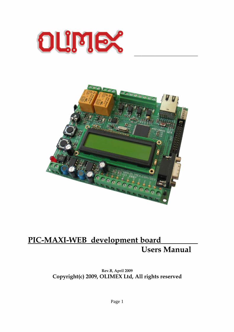
PIC-MAXI-WEB development board Users Manual
Rev.B, April 2009Copyright(c) 2009, OLIMEX Ltd, All rights reserved
Page 1

INTRODUCTION:
This board allows you to easily develop Ethernet connectivity applications.It has everything you normally would need for such applications: powerrelays which you can command through web interface, LCD display whichwill display messages you fill in web forms, analogue inputs for connectionto sensors, digital optoisolated inputs, trimmer potentiometer, temperaturesensor, Ethernet connector. With this board you can easily automate yourhome and then control and monitor it from any point in the world viaInternet. An extension connector is available so you can connect custommade hardware to the board. The PIC18F97J60 has 128KB Flash programmemory and there is external 1Mbit (128KB) flash memory for data storage.The on board DC/DC converter makes this board very tolerant to theexternal power supply which could be in 9-25V DC or 7-18V AC range. Thebridge rectifier on the input allows AC and DC adapters to be used andmakes power supply polarity problems go away.
BOARD FEATURES:
- PIC18F97J60 microcontroller with embedded Ethernet MACand PHY and 128KB Flash programming space - 1Mbit on board serial flash for web pages storage - ICSP/ICD connector for programming and debugging with PIC-ICD2 and PIC-ICD2-POCKET. - Temperature sensor - Trimmer potentiometer connected to analogue input - Two relays 10A/250VAC - Four optoisolated digital inputs - Twelve analogue inputs on terminal block - Two buttons - LCD16x2 with backlight - RS232 interface - Ethernet interface - Complete web server and TCP-IP stack support as perMicrochip's open source TCP-IP stack - Terminal block for power supply works with 9-25 VDC powersupply - Extension header to connect to other boards - Dimensions 120x108 mm (4.72x4.25")
ELECTROSTATIC WARNING:
The PIC-MAXI-WEB board is shipped in protective anti-static packaging.The board must not be subject to high electrostatic potentials. Generalpractice for working with static sensitive devices should be applied whenworking with this board.
BOARD USE REQUIREMENTS:
Cables: Depends on the used programming/debugging tool. It couldbe 1.8 meter USB A-B cable to connect PIC-ICD2-POCKET or PIC-ICD2 toUSB host on PC or RS232 cable for PIC-ICD2-TINY and PIC-ICD2. You will
Page 2

need a serial cable if not for programming, than for configuring the board.You will also need a LAN cable.
Hardware: Programmer/Debugger –Olimex programmers are applicable,for example PIC-ICD2, PIC-ICD2-POCKET, PIC-ICD2-TINY orother compatible programming/debugging tool.
!!!Warning!!! When you want to program this microcontroller with PIC-ICD2, PIC-ICD2-POCKET or PIC-ICD2-TINY, beforeconnecting the programmer to your target board, you shouldfirst connect the programmer to your computer and openMPLAB. There, first from menu Configure – Select Device –choose the microcontroller you are about to program, then frommenu Programmer – Select Programmer – choose MPLAB ICD2, wait while MPLAB is downloading operation system, andafter ICD2 is connected – check in menu Programmer –Settings – Power – there is option – Power target circuit fromMPLAB ICD 2 – this option should be forbidden, you could notselect it. Now it is safe to connect the programmer to yourtarget board.
Software: PIC-WEB is tested with MPLAB IDE v.7.62 + MPLAB C18 Ccompiler. It is possible that the stack might not functionproperly if used with later versions of MPLAB IDE.You will also need a terminal program configured at 19 200bps, 8N1 and no flow control.
PROCESSOR FEATURES:
PIC-MAXI-WEB board use MCU PIC18F97J60 from Microchip with thesefeatures:- IEEE 802.3 compatible Ethernet Controller- Integrated MAC and 10Base-T PHY- 8-Kbyte Transmit/Receive Packet Buffer SRAM- Supports One 10Base-T Port- Programmable Automatic Retransmit on Collision- Programmable Padding and CRC Generation- Programmable Automatic Rejection of Erroneous Packets- Activity Outputs for 2 LED Indicators- Buffer:
o Configurable transmit/receive buffer sizeo Hardware-managed circular receive FIFOo Byte-wide random and sequential accesso Internal DMA for fast memory copyingo Hardware assisted checksum calculation for various protocols
- MAC:o Support for Unicast, Multicast and Broadcast packetso Programmable Pattern Match of up to 64 bytes within packet at
user-defined offseto Programmable wake-up on multiple packet formats
- PHY:
Page 3

o Wave shaping output filter- Selectable System Clock derived from Single 25 MHz External Source:
o 2.778 to 41.667 MHz- Internal 31 kHz Oscillator- Secondary Oscillator using Timer1 @ 32 kHz- Fail-Safe Clock Monitor:
o Allows for safe shutdown if oscillator stops- Two-Speed Oscillator Start-up- Address Capability of up to 2 Mbytes for External Memory Bus- 8-Bit or 16-Bit Interface- 2-Bit, 16-Bit and 20-Bit Addressing modes- High-Current Sink/Source: 25 mA/25 mA on PORTB and PORTC- Five Timer modules (Timer0 to Timer4)- Four External Interrupt pins- Two Capture/Compare/PWM (CCP) modules- Three Enhanced Capture/Compare/PWM (ECCP) modules:
o One, two or four PWM outputso Selectable polarityo Programmable dead timeo Auto-shutdown and auto-restart
- Up to Two Master Synchronous Serial Port (MSSP) modules supportingSPI (all 4 modes) and I2C™ Master and Slave modes
- Up to Two Enhanced USART modules:o Supports RS-485, RS-232 and LIN 1.2o Auto-wake-up on Start bito Auto-Baud Detect (ABD)
- 10-Bit, Up to 16-Channel Analog-to-Digital Converter module (A/D):o Auto-acquisition capabilityo Conversion available during Sleep
- Dual Analog Comparators with Input Multiplexing- Parallel Slave Port (PSP) module (100-pin devices only)- 5.5V Tolerant Inputs (digital-only pins)- Low-Power, High-Speed CMOS Flash Technology:
o Self-reprogrammable under software control- C compiler Optimized Architecture for Reentrant Code- Power Management Features:
o Run: CPU on, peripherals ono Idle: CPU off, peripherals ono Sleep: CPU off, peripherals off
- Priority Levels for Interrupts- 8 x 8 Single-Cycle Hardware Multiplier- Extended Watchdog Timer (WDT):
o Programmable period from 4 ms to 134s- Single-Supply 3.3V In-Circuit Serial Programming™ (ICSP™) via Two
Pins- In-Circuit Debug (ICD) with 3 Breakpoints via Two Pins- Operating Voltage Range of 2.35V to 3.6V (3.1V to 3.6V using Ethernet
module)- On-Chip 2.5V Regulator
Page 4

BLOCK DIAGRAM:
Page 5

MEMORY MAP:
Page 6

Page 7

SCHEMATIC:
Page 8
10K
100nF
100nNA NA NA NA NA NA
100nF
100nF
470pF
100n
NA
33pF
100n
100n
100n
100n
100n
33pF
1000uF/6.3V/8mm
220u/25V
100nF
15pF
15pF
100nF 100nF
100n 100n
100nF 100nF 100nF
100nF 100nF
100nF
100nF
100nF
100nF
NA NA NA NA
NA
470pF
1000uF/6.3V/8mm
220u/25V
47uF/6.3V
10uF/6.3V 10uF/6.3V
10k
1N58
19
1N4148
1N4148
1N4148
1N4148
1N4148
1N58
19
1N4148
B-DIL3
CON62.54-0-D
ferrite bead
CL150uH/SW68CL150uH/SW68
RJLD-043TC
yellowREDRED
red
red
red
red
green
green
H11A817SMD
H11A817SMD
H11A817SMD
H11A817SMD
+5V
+5V
+5V
+5V
RED
25MHz
32768/6pF
BC817
BC817
100k
1k
49.9/1%49.9/1%
49.9/1%
49.9/1%
180
180
1k
10K
0.68
0.68
10K
330
330
0.68
330
1k
330
10K
330
0.68
10K
10K
330
3.0k/1%
1k/1%
3k/1%
1.8k/1%
1.5K
10K
330 10K
330
1k
1M
0
opt
10K
330 10K
270/1%
10K
2k/1%
100k 100k
10K
330
opt
330
330
330
330 330 330
270
0
330
4.7k 4.7k
RAS-05-15
RAS-05-15
DB9_female
BC846
TERMISTOR
MC34063AP1/ACN_MBR
PIC18F97J60
MC34063AP1/ACN_MBR
ST3232
AT45DB011
3.3V
3.3V
3.3V
3.3V3.3V
3.3V
3.3V
3.3V
3.3V
3.3V
3.3V
3.3V
3.3V 3.3V
3.3V
3.3V
3.3V
3.3V
3.3V
3.3V
3.3V
AVDD
DB[0..7],RS,R/W,E,LIGHT_LCD
#SS1
#SS1
#SS2
#SS2
AIN2
AIN2AIN3
AIN3
AIN4
B1
B1
B2
B2
CS
CS
DB0
DB0
DB1
DB1
DB2
DB2
DB3
DB3
DB4
DB4
DB5
DB5
DB6
DB6
DB7
DB7
D_IN1
D_IN1
D_IN2
D_IN2
D_IN3
D_IN3
D_IN4
D_IN4
E
E E
LEDA
LEDA
LEDB
LEDB
LIGHT_LCD
LIGHT_LCD LIGHT_LCD
MISO
MISO
MOSI
MOSI
OUT1
OUT1
OUT2
OUT2
PGC
PGC
PGD
PGD
R/W
R/W R/W
RS
RS RS
RST
RST
RST
RXD
RXD
SCK
SCK
TPIN+
TPIN+
TPIN-
TPIN-
TPOUT+
TPOUT+
TPOUT-
TPOUT-
TXD
TXD
1
2
3#S
S1/
#SS
2
12
3.3V
_E
12
5V_E
AN_TR BUT1 BUT2
C1
C2
C3 C4 C5 C6 C7 C8
C9
C10
C11
C12
C13
C14
C15
C16
C17
C18
C19
C20
C23
C24
C25
C26
C27
C28 C29
C30 C31
C32 C33 C34
C35 C36
C37
C38
C39
C40
C41 C42 C43 C44
C45
C46C47
C48
C49
C50 C51
CONTRAST
D1
D2
D3
D4
D5
D6
D7
D8
EXT-1EXT-2
EXT-3EXT-4EXT-5EXT-6EXT-7EXT-8EXT-9EXT-10
EXT-11
EXT-12EXT-13EXT-14EXT-15
EXT-16
EXT-17EXT-18EXT-19EXT-20EXT-21EXT-22EXT-23
EXT-24
EXT-25EXT-26
G1
123456
ICSP
IN1-1
IN1-2
IN2-1
IN2-2
IN3-1
IN3-2
IN4-1
IN4-2
L1
L2L3
AGAG
AYAY KGKG
KYKY
RCT6 RD+7
RD-8
TCT3 TD+1
TD-275 75
75 75
1nF/2kV
1452
3786
GREEN
YELLOW
LAN
A 15
DB07
DB18
DB29
DB310
DB411
DB512
DB613
DB714
E6
K 16
R/W5
VD
D2
VO3
VS
S1
_RS4
LD0LD1LD2
LED1
LED2
LED3
LED4
LED5
LED6
1
2
4
3
OPT1
1
2
4
3
OPT2
1
2
4
3
OPT3
1
2
4
3
OPT4
OUT1-1
OUT1-2
OUT1-3
OUT2-1
OUT2-2
OUT2-3
PWR-1
PWR-2
PWR_LED
Q1
Q2
Q3
Q4
R1
R2
R3R4
R5
R6
R7
R8
R9
R10
R11
R12
R13
R14
R15
R16
R17
R18
R19
R20
R21
R22
R23
R24
R25
R26
R27
R28
R29
R30
R31
R32 R33
R34
R35
R36
R37
R38
R39
R40 R41
R42
R43
R44
R45 R46
R47
R48
R49
R50
R51
R52
R53 R54 R55
R56
R57
R58
R59 R60
REL1
REL1
REL2
REL2
12345
6789
RS232
RST
T3
TH1
DC
8
FB5
IS7
SC1
SE2TC3
VC
C6
VS
S4
U1
#MCLR13
AVDD30
AVSS31
ENVREG29
NC9
OSC1/CLKI63
OSC2/CLKO64
RA0/LEDA/AN035
RA1/LEDB/AN134
RA2/AN2/VREF-33
RA3/AN3/VREF+32
RA4/T0CKI42
RA5/AN441
RB0/INT0/FLT05
RB1/INT16
RB2/INT27
RB3/INT3/ECCP2(1)/P2A(1)8
RB4/KBI069
RB5/KBI168
RB6/KBI2/PGC67
RB7/KBI3/PGD57
RBIAS80
RC0/T1OSO/T13CKI44
RC1/T1OSI/ECCP2(1)/P2A(1)43
RC2/ECCP1/P1A53
RC3/SCK1/SCL154
RC4/SDI1/SDA155
RC5/SDO156
RC6/TX1/CK145
RC7/RX1/DT146
RD0/AD0/PSP092
RD1/AD1/PSP191
RD2/AD2/PSP290
RD3/AD3/PSP389
RD4/AD4/PSP4/SDO288
RD5/AD5/PSP5/SDI2/SDA287
RD6/AD6/PSP6/SCK2/SCL284
RD7/AD7/PSP7/#SS283
RE0/AD8/#RD/P2D4
RE1/AD9/#WR/P2C3
RE2/AD10/#CS/P2B98
RE3/AD11/P3C(2)97
RE4/AD12/P3B(2)96
RE5/AD13/P1C(2)95
RE6/AD14/P1B(2)94
RE7/AD15/ECCP2(1)/P2A(1)93
RF0/AN512
RF1/AN6/C2OUT28
RF2/AN7/C1OUT23
RF3/AN822
RF4/AN921
RF5/AN10/CVREF20
RF6/AN1119
RF7/#SS118
RG0/ECCP3/P3A71
RG1/TX2/CK270
RG2/RX2/DT252
RG3/CCP4/P3D51
RG4/CCP5/P1D14
RG511
RG610
RG738
RH0/A1699
RH1/A17100
RH2/A181
RH3/A192
RH4/AN12/P3C(2)27
RH5/AN13/P3B(2)26
RH6/AN14/P1C(2)25
RH7/AN15/P1B(2)24
RJ0/ALE49
RJ1/#OE50
RJ2/#WRL66
RJ3/#WRH61
RJ4/BA047
RJ5/#CE48
RJ6/#LB58
RJ7/#UB39
TPIN+74TPIN-73
TPOUT+78 TPOUT-77
VDD17
VDD137
VDD259
VDD362
VDD486
VDDCORE/VCAP16
VDDPLL81
VDDRX75 VDDTX76
VSS15
VSS136
VSS240
VSS360
VSS465
VSS585
VSSPLL82
VSSRX72 VSSTX79
U2
DC
8
FB5
IS7
SC1
SE2TC3
VC
C6
VS
S4
U3
C1+ 1
C1- 3
C2+ 4
C2- 5
R1IN13 R1OUT 12
R2IN8 R2OUT 9
T1IN 11T1OUT
14
T2IN 10T2OUT
7
V+2
V-6
U4
15 16GND VCCU4PWR
/CS/4
/RESET/3
/WP/5
GND7SCK2
SI1SO
8
VCC6
U5
X1-1
X1-2X2-1X2-2X3-1X3-2X4-1X4-2
X5-1X5-2X6-1X6-2X6-3
PIC-MAXI-WEBRev. B
COPYRIGHT(C) 2009, Olimex Ltd.
http://www.olimex.com/dev
+
+
+
+
+
+ +
RJ4
5 S
IDE
1:1
1:1
GND
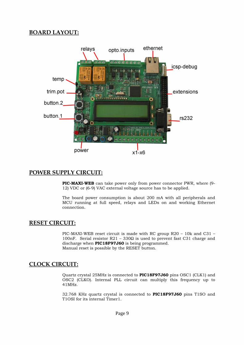
BOARD LAYOUT:
POWER SUPPLY CIRCUIT:
PIC-MAXI-WEB can take power only from power connector PWR, where (9-12) VDC or (6-9) VAC external voltage source has to be applied.
The board power consumption is about 200 mA with all peripherals andMCU running at full speed, relays and LEDs on and working Ethernetconnection.
RESET CIRCUIT:
PIC-MAXI-WEB reset circuit is made with RC group R20 – 10k and C31 –100nF. Serial resistor R21 – 330Ω is used to prevent fast C31 charge anddischarge when PIC18F97J60 is being programmed. Manual reset is possible by the RESET button.
CLOCK CIRCUIT:
Quartz crystal 25MHz is connected to PIC18F97J60 pins OSC1 (CLK1) andOSC2 (CLKO). Internal PLL circuit can multiply this frequency up to41MHz.
32.768 KHz quartz crystal is connected to PIC18F97J60 pins T1SO andT1OSI for its internal Timer1.
Page 9

JUMPER DESCRIPTION:
5V_E enables 5V supply for LCD and relays.Default state closed (shorted).
3.3V_E enables 3.3V supply for PIC18F97J60 and all other devices. Default state closed (shorted). 3.3V is also available to EXT-1,
so if you want to connect external backup battery to thePIC18F97J60 this jumper should be opened and the externalbattery to be connected to EXT-1 pin.
#SS1/#SS2 chip select for U5 (AT45DB011) serial flash. Default position is selected to be #SS2 in compatibles with Microchip
software but user can change it in its own application. Default state closed (shorted)
INPUT/OUTPUT:
Two User buttons with names BUT1 and BUT2 – connected toPIC18F97J60 pin 8 RB3/INT3/ECCP2(1)/P2A(1) and pin 6 RB1/INT1;
One analog trimmer AN_TR – connected to PIC18F97J60 pin 33RA2/AN2/VREF-;
Thermistor TH1– connected to PIC18F97J60 pin 32 RA2/AN2/VREF+;
Three LEDs – LD0 (yellow) – connected to PIC18F97J60 pin 49 RJ0/ALE ,LD1 (red) – connected to PIC18F97J60 pin 50 RJ1/#OE, LD2 (red) –connected to PIC18F97J60 pin 66 RJ2/#WRL;
Four opto isolated digital inputs IN1-IN4;
Four red LEDs – LED1, LED2, LED3, LED4 for every digital input;
Two green LEDs – LED5, LED6 – for the relays;
Power supply red LED with name PWR_LED – indicates that 3.3V powersupply is available
Twelve analog inputs X1-X6;
LCD Display - SC1602A - 16 characters x 2 lines.
Page 10

EXTERNAL CONNECTOR DESCRIPTION:
ICSP:
Pin # Signal Name
1 RST
2 VCC
3 GND
4 PGD
5 PGC
6 NC
PGD I/O Program Data. Serial data for programming.PGC Input Program Clock. Clock used for transferring the serial data (output from
ICSP, input for the MCU).
RS232:
Pin # Signal Name
1 NC
2 TXD
3 RXD
4 NC
5 GND
6 NC
7 NC
8 NC
9 NC
TXD OutputTransmit Data. This is the asynchronous serial data output (RS232) for the shift register on the UART controller.
RXD Input Receive Data. This is the asynchronous serial data input (RS232) for the shift register on the UART controller.
Page 11

X(1 ÷ 6)-CONNECTORS
Pin # Signal Name
1 AIN4
2 AIN5
3 AIN6
4 AIN7
5 AIN8
6 AIN9
7 AIN10
8 AIN11
9 AIN12
10 AIN13
11 AIN14
12 AIN15
13 GND
These are the 12 analog inputs.
IN(1 ÷ 4)-CONNECTORS
Pin # Signal Name
1 IN1+
2 IN1-
3 IN2+
4 IN2-
5 IN3+
6 IN3-
7 IN4+
8 IN4-
These are the 4 opto isolated digital inputs.
Page 12

EXT:
Pin # Signal Name Pin # Signal Name
1 VCC 2 GND
3 RJ7/#UB 4 RJ6/#LB
5 RJ5/#CE 6 RJ4/BA0
7 RJ3/#WRH 8 RJ2/#WRL
9 RJ1/#OE 10 RJ0/ALE
11 RH3/A19 12 PG3/CCP4/P3D
13 RG2/RX2/DT2 14 RG1/TX2/CK2
15 RG0/ECCP3/P3A 16 RF7/#SS1
17 RD6/AD6/PSP6/SCK2/SCL2 18 RD5/AD5/PSP5/SDI2/SDA2
19 RD4/AD4/PSP4/SDO2 20 RD3/AD3/PSP3
21 RD2/AD2/PSP2 22 RS1/AD1/PSP1
23 RD0/AD0/PSP0 24 RB5/KBI1
25 RB0/INT0/FLT0 26 RB2/INT2
Page 13

LAN :
Pin # Signal Name Chip Side Pin # Signal Name Chip Side
1 TPOUT+ 5 Not Connected (NC)
2 TPOUT- 6 Not Connected (NC)
3 3.3V 7 TPIN+
4 Not Connected (NC) 8 TPIN-
LED Color Usage
Right Yellow Activity
Left Green 100MBits/s (Half/Full duplex)
RELAYS:
Page 14
Pin # Signal Name
1 Normal Open
2 Common
3 Normal Close

PWR :
Page 15
Pin # Signal Name
1 AC in 1
2 AC in 2

MECHANICAL DIMENSIONS:
All measures are in mm.
Page 16
AVAILABLE DEMO SOFTWARE:
You could find information about PIC-MAXI-WEB board, Microchip TCP/IPstack and how to change and configure the software in Understanding PIC WEB boards onwww.olimex.com/dev.
Page 17

ORDER CODE:
PIC-MAXI-WEB – assembled and tested (no kit, no soldering required)
How to order?
You can order to us directly or by any of our distributors.
Check our web www.olimex.com/dev for more info.
All boards produced by Olimex are RoHS compliant
Revision history:
REV.A - created July 2008
REV B - created April 2009
Page 18

Disclaimer:
© 2009 Olimex Ltd. All rights reserved. Olimex®, logo and combinations thereof, areregistered trademarks of Olimex Ltd. Other terms and product names may be trademarks ofothers.
The information in this document is provided in connection with Olimex products. Nolicense, express or implied or otherwise, to any intellectual property right is granted by thisdocument or in connection with the sale of Olimex products.
Neither the whole nor any part of the information contained in or the product described inthis document may be adapted or reproduced in any material from except with the priorwritten permission of the copyright holder.
The product described in this document is subject to continuous development andimprovements. All particulars of the product and its use contained in this document aregiven by OLIMEX in good faith. However all warranties implied or expressed including butnot limited to implied warranties of merchantability or fitness for purpose are excluded.
This document is intended only to assist the reader in the use of the product. OLIMEX Ltd.shall not be liable for any loss or damage arising from the use of any information in thisdocument or any error or omission in such information or any incorrect use of the product.
Page 19