Embed Size (px)
Citation preview
190 Journal of Power Electronics, Vol. 16, No. 1, pp. 190-204, January 2016
http://dx.doi.org/10.6113/JPE.2016.16.1.190
ISSN(Print): 1598-2092 / ISSN(Online): 2093-4718
JPE 16-1-21
PI Controlled Active Front End Super-Lift Converter with Ripple Free DC Link for Three Phase Induction
Motor Drives
Elangovan P.† and Nalin Kant Mohanty*
†Department of EEE, S. K. P. Engineering College, Anna University, India *Department of EEE, Sri Venkateswara College of Engineering, Anna University, India
Abstract
An active front end (AFE) is required for a three-phase induction motor (IM) fed by a voltage source inverter (VSI), because of the increasing need to derive quality current from the utility end without sacrificing the power factor (PF). This study investigates a proportional-plus-integral (PI) controller based AFE topology that uses a super-lift converter (SLC). The significance of the proposed SLC, which converts rectified AC supply to geometrically proceed ripple-free DC supply, is explained. Variations in several power quality parameters in the intended IM drive for 0% and 100% loading conditions are demonstrated. A simulation is conducted by using MATLAB/Simulink software, and a prototype is built with a field programmable gate array (FPGA) Spartan-6 processor. Simulation results are correlated with the experimental results obtained from a 0.5 HP IM drive prototype with speed feedback and a voltage/frequency (V/f) control strategy. The proposed AFE topology using SLC is suitable for three-phase IM drives, considering the supply end PF, the DC-link voltage and current, the total harmonic distortion (THD) in supply current, and the speed response of IM. Key words: Active front end, DC-link fluctuations, Induction motor drives, PI controller, Total harmonic distortion
I. INTRODUCTION
In modern years, induction motor (IM) drives have been playing a significant role in industrial applications because of advances in power semiconductor devices. However, the use of IM drives is challenging because of their complex model, nonlinear behavior during saturation, and electrical parameter oscillation that depends on environmental factors. In the abovementioned aspects, poor power factor (PF), supply end current distortion, and DC-link fluctuations play dominant roles in the control of VSI, which feed IM. A poor PF is a consequence of a significant phase difference between the voltage and the current across load terminals, or it is due to high harmonic content or distorted current. The basic aims of improving PF are to reduce greenhouse gas emissions and the electricity bills of consumers, to avail additional
kilovolt-ampere from existing supply, and to extend equipment life. References [1]–[4] developed a PF correction circuit with supply current total harmonic distortion (THD) under the IEEE-519 limit, but they failed to concentrate on fluctuations in DC-link voltage and current. The active damping technique using a DC-link capacitor [5] seems to be simple and effective for regulating DC-link oscillations, but shortcomings occur when the load on the motor changes and can result in under or over correction; this technique is unsuitable for adjustable-speed drives. The influence of DC-link fluctuations on three-phase IM drives was explained clearly in [6], which concluded that the oscillation of DC-link parameters affected the THD in supply and motor current. Traditionally, the front end of a VSI-fed IM drive is connected with a diode bridge rectifier (DBR) [7], [8], which produces fixed DC from fixed AC supply. Advances in power electronic devices have enabled the DBR to be replaced with a phase-controlled rectifier (PCR) that converts variable DC from fixed AC supply [9]. Conversely, the regulation of DC-link parameters using PCR presents several limitations, such as low DC-link voltage and ripple in DC-link voltage
Manuscript received May 20, 2015; accepted Aug. 12, 2015 Recommended for publication by Associate Editor Dong-Hee Lee.
†Corresponding Author: [email protected] Tel: +91-4175-252633, Fax: +91-4175-252643, Anna University
*Department of EEE, Sri Venkateswara College of Engineering, Anna University, India
© 2016 KIPE

PI Controlled Active Front End … 191
and current. Invariable DC-link voltage is mandatory in a PCR system to obtain a high performance of the IM drive because the voltage oscillation in DC link division causes a voltage error at IM terminals.
A distinctive method to prevent voltage oscillation is to introduce a DC–DC converter between the PCR and the VSI of a drive system. The DC–DC boost converter employed in [10] produced 120 V DC for 70 V DC input, whereas the boost converter depicted in [11] showed only 91% efficiency with a complex topology. An advanced DC–DC converter in a super-lift Luo converter series [12], [13], named super-lift converter (SLC), which produces output voltage in geometric progression rather than arithmetic progression [14], overcomes the problems that exist in conventional boost converters. However, the SLC is inefficient when used in an open-loop system. Reference [15] developed a strategy to control the SLC by using a proportional-plus-integral (PI) regulator, but the strategy failed to improve SLC under load and line variations.
This study implements an improved PI-control based active front end (AFE) topology for IM drives using an SLC. Simulation is conducted using MATLAB/Simulink software. A prototype using a field programmable gate array (FPGA) Spartan-6 processor is developed to validate the simulation results. The proposed IM drive has the following features:
Operation of IM drives with a unity PF at the supply end
An improved THD in the supply current A DC-link voltage level 1.5 times greater than that
of the conventional DC–DC converters Ripple-free DC-link voltage and current
II. VOLTAGE-LIFTING ROLE OF DC–DC CONVERTERS IN IM DRIVES
The foremost concentration of this work is quality DC–DC power conversion in the front end of a VSI-fed IM drive without sacrificing PF at the supply end. This section explains the voltage-lifting role of DC-DC converters in IM drives to bridge the research gap between the conventional and the proposed approaches.
Voltage regulation with a wide boost-up ratio plays a vital part in IM drives. Considering the fact that low-cost and high-efficiency design of an IM drive requires quality DC-link parameters and to fulfill it, a DC-DC converter is introduced in the IM drive. The conventional system [16], which uses a back-to-back converter with an average DC-link voltage, is
3VaV = cosαo π, (1)
where Va is the input AC voltage,
α is the firing angle of the converter, and
Vo is the DC-link voltage.
For approximation, the arrangement of 1 phase, 230 V, and 50 Hz AC input supply will produce approximately 220 V DC when the firing angle “α” is 0°. The attained 220 V DC fed in a VSI working in 180° mode will produce an average output line voltage given by
2π32 2= dθVV oL 2π 0
2= Vo3
, (2)
V = 0.8165 VL o . (3)
Hence, the line voltage at the stator terminals of IM is limited to 179.63 V AC. Without the DC–DC converter in the IM drive, the conventional back-to-back converter arrangement will produce only 77.97% voltage transfer.
To introduce a boost converter between the PCR and the VSI for the same arrangement discussed above, the DC-link voltage is given by
3V1 aV = cosαo 1 π , (4)
where γ is the conduction duty of the DC–DC converter.
For γ = 0.5, the boost converter-intended IM drive scheme
produces a line voltage twice that of the PCR-fed IM drive
and is given by
= 1.633 V VL o . (5)
The implementation of an advanced DC–DC converter in the front end of the VSI produces a wide range of DC-link voltage pump-up, which is validated in the following chapter.
III. PROPOSED IM DRIVE SCHEME
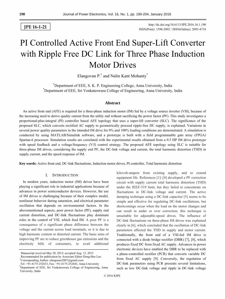
A schematic of the proposed IM drive is shown in Fig. 1. The complete system is divided into three stages. The first stage converts single-phase AC power into fixed DC power using a DBR. The second stage converts the invariable DC power from the DBR to variable DC using an SLC. The last stage converts the DC power from the SLC to variable voltage/variable frequency AC power using a VSI. The following subsections explain (A) the gate control strategy of the SLC using a PI controller, (B) the gate control strategy of the VSI in the proposed system, and (C) the design deliberation of the inductor L21 and the capacitor Co of the SLC.
A. Gate Control Strategy of the Proposed SLC
The positive-output SLC [17] has some subseries, such as the main, additional, enhanced, re-enhanced, and multiple-enhanced series. The elementary circuit from the
192 Journal of Power Electronics, Vol. 16, No. 1, January 2016
Proposed Active Front End
Topology
Gate Pulse
V/f Control
Gate Pulse
DBR SLC VSI
3 Phase
IM
1 Phase,
100V,50Hz
ACSupply
Sensed Speed
of IM
L11
D21 D22
L21 C21 C0
S
32
1_
+
Fig. 1. Schematic of the proposed IM drive.
main series is adopted for the proposed system.
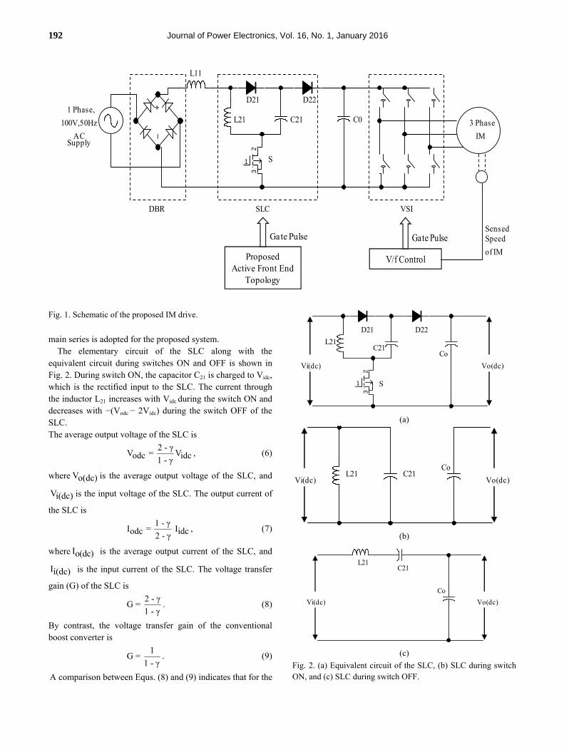
The elementary circuit of the SLC along with the equivalent circuit during switches ON and OFF is shown in Fig. 2. During switch ON, the capacitor C21 is charged to Vidc, which is the rectified input to the SLC. The current through the inductor L21 increases with Vidc during the switch ON and decreases with −(Vodc − 2Vidc) during the switch OFF of the SLC. The average output voltage of the SLC is
2 - γV = Vodc idc1 - γ
, (6)
where Vo(dc) is the average output voltage of the SLC, and
Vi(dc) is the input voltage of the SLC. The output current of
the SLC is
1 - γI = Iodc idc2 - γ
, (7)
where Io(dc) is the average output current of the SLC, and
Ii(dc) is the input current of the SLC. The voltage transfer
gain (G) of the SLC is
2 - γG =
1 - γ. (8)
By contrast, the voltage transfer gain of the conventional boost converter is
1G =
1 - γ. (9)
A comparison between Equs. (8) and (9) indicates that for the
32
1
D21 D22
L21C21
Co
S
Vi(dc) Vo(dc)
(a)
L21 C21Co
Vi(dc) Vo(dc)
(b)
L21C21
Co
Vi(dc) Vo(dc)
(c)
Fig. 2. (a) Equivalent circuit of the SLC, (b) SLC during switch ON, and (c) SLC during switch OFF.
PI Controlled Active Front End … 193
same conduction duty, the SLC produces 1.5 times higher voltage transfer than the conventional boost converter. The ripple current of the inductor “L21” is
V - 2 Vodc idcΔi = TL off21 L21
, (10)
where Toff is the OFF time of the SLC. From Equ. (3), the line voltage of the VSI with respect to the DC input of the SLC is
0.8165 (2 - γ) VidcV = L 1 - γ, (11)
where the variable Vidc is equal to Vo, which is mentioned in Equ. (3). By substituting γ = 0.5 into Equ. (11), we obtain
= 2.4495 V VL idc . (12)
A comparison among Equs. (3), (5), and (12) implies that the SLC adopted system attains voltage at IM terminals at a massive level in contrast to the adopted system of the conventional DC-DC converters.
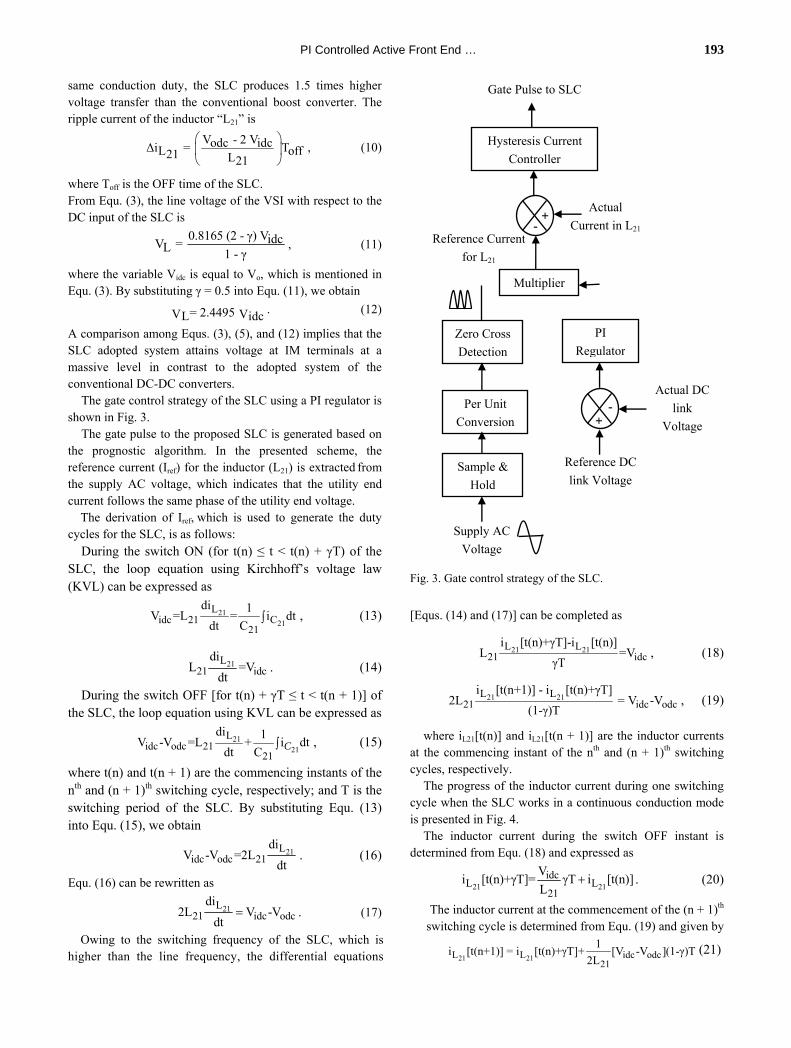
The gate control strategy of the SLC using a PI regulator is shown in Fig. 3.
The gate pulse to the proposed SLC is generated based on the prognostic algorithm. In the presented scheme, the reference current (Iref) for the inductor (L21) is extracted from the supply AC voltage, which indicates that the utility end current follows the same phase of the utility end voltage.
The derivation of Iref, which is used to generate the duty cycles for the SLC, is as follows:
During the switch ON (for t(n) ≤ t < t(n) + γT) of the SLC, the loop equation using Kirchhoff’s voltage law (KVL) can be expressed as
2121
Lidc 21 C
21
di 1V =L = i dt
dt C , (13)
21L21 idc
diL =V
dt. (14)
During the switch OFF [for t(n) + γT ≤ t < t(n + 1)] of the SLC, the loop equation using KVL can be expressed as
2121
Lidc odc 21
21
di 1V -V =L + i dt
dt C C , (15)
where t(n) and t(n + 1) are the commencing instants of the nth and (n + 1)th switching cycle, respectively; and T is the switching period of the SLC. By substituting Equ. (13) into Equ. (15), we obtain
21Lidc odc 21
diV -V =2L
dt. (16)
Equ. (16) can be rewritten as
21L21 idc odc
di2L V -V
dt . (17)
Owing to the switching frequency of the SLC, which is higher than the line frequency, the differential equations
Fig. 3. Gate control strategy of the SLC.
[Equs. (14) and (17)] can be completed as
21 21L L21 idc
i [t(n)+γT]-i [t(n)]L =V
γT, (18)
21 21L L21 idc odc
i [t(n+1)] - i [t(n)+γT]2L = V -V
(1-γ)T, (19)
where iL21[t(n)] and iL21[t(n + 1)] are the inductor currents at the commencing instant of the nth and (n + 1)th switching cycles, respectively.
The progress of the inductor current during one switching cycle when the SLC works in a continuous conduction mode is presented in Fig. 4.
The inductor current during the switch OFF instant is determined from Equ. (18) and expressed as
21 21idc
L L21
Vi [t(n)+γT]= γT i [t(n)]
L . (20)
The inductor current at the commencement of the (n + 1)th switching cycle is determined from Equ. (19) and given by
21 21L L idc odc21
1i [t(n+1)] = i [t(n)+γT]+ [V -V ](1-γ)T
2L(21)
Gate Pulse to SLC
Hysteresis Current
Controller
Multiplier
Zero Cross
Detection
PI
Regulator
Per Unit
Conversion
Sample &
Hold
Supply AC
Voltage
Reference DC
link Voltage
Actual DC
link
Voltage +-
+-
Reference Current
for L21
Actual
Current in L21

194 Journal of Power Electronics, Vol. 16, No. 1, January 2016
Fig. 4. Inductor current in one switching cycle.
By substituting Equ. (20) into Equ. (21), we can derive the
inductor current at the commencement of the (n + 1)th switching cycle in terms of the inductor current at the commencement of the nth switching cycle as
21 21L L idc odc idc21 21
1 1i [t(n+1)] = i [t(n)]+ [V -V (1-γ)]T- V .γ.T
2L L
.
(22) Equ. (22) in a discrete form is represented by
21 21idc odc
L L21
V (1-2γ)T-V (1-γ)Ti (n+1) = i (n)+
2L. (23)
From Equ. (23), the inductor current at the commencement of the subsequent switching cycle is determined by the inductor current at the beginning of the current switching cycle, the conduction duty cycle, the input voltage, and the output voltage. The conduction duty cycle (γ) is derived from Equ. (23) and expressed as
21 2121 L L odc idc
odc idc odc idc
2L [i (n+1)-i (n)] V -Vγ = +
(V -2V )T V -2V
. (24)
Equ. (24) depicts the conduction duty cycle of the SLC, in which the rectified current from utility AC supply [iL21(n + 1)] and the output voltage of the SLC [Vodc] follow Iref and Vref. Hence, the conduction duty cycle is represented as
2121 ref L ref idc
ref idc ref idc
2L [i (n+1)-i (n)] V -Vγ = +
(V -2V )T V -2V
. (25)
The reference current can be expressed as
21L P li (n+1) = M sin(φ .t(n+1) , (26)
where MP is the peak value of the reference inductor (L21) current, which is multiplied with the rectified sinusoidal waveform (sin (φl.t (n + 1)) to generate iL21(n + 1).
The PI regulator for the projected SLC is designed by finding appropriate values of proportional gain (Kp) and integral time (Ti). The first step in determining Kp and Ti is to develop a state model of the SLC.
The state model of the SLC [18], [19] is determined by assuming the state variables x1 (current flowing through L21), x2 (voltage across C21), and x3 (voltage across Co), and the
0 0.05 0.1 0.15 0.2 0.250
0.2
0.4
0.6
0.8
1
Time (s)
Out
put
Res
pons
e
Step Response of SLC
T = 5.2msL = 5ms
Tangential Line
Fig. 5. S-shaped step response of the SLC.
input variable u (input voltage of the SLC). Considering the negligible input and the output resistance of the proposed SLC, the state equation of the SLC during the switch ON is
given by
.
2111.
2 22121.
33
10 0 0
1 10 0
010 0
o
x Lx
x x uC C
xx
C
, (27)
and the state equation of the SLC during the switch OFF is
.
1 21 211 21.
2 221
. 33
1 10 1
10 0 0
01 1
0o o
x L L x Lx x u
Cx
xC C
. (28)
The state-space averaging model of the SLC is
.
1 21 21 21 211
.
2 221 21 21
. 33
1 1 1 1
1 20
1 1 10
o o o
x L L L Lx
x x uC C C
xx
C C C
. (29)
On the basis of the Zeigler–Nichols tuning method [20], Kp and Ti are resolved by applying the step input to the mathematical model [Equ. (29)] of the SLC to attain an S-shaped curve, as shown in Fig. 5. Drawing a tangential line to the S-shaped curve obtains constants, namely, delay time (L = 0.005 s) and time constant (T = 0.052 s). The values L and T are used to extract the constants Kp (9.36) and Ti (0.016 s) from the Zeigler–Nichols chart.
Single-phase supply voltage is also involved in the topology to generate the reference current for the inductor L21.
iL21
iL21[t(n)+γT]
iL21[t(n+1)]
t(n) t(n)+γT t(n+1)
iL21[t(n)]
PI Controlled Active Front End … 195
The supply voltage is sampled by using a sample-hold circuit and converted to per unit (p.u.) form. The amplitude of the negative half cycle in the p.u. voltage waveform is shifted to a positive half cycle by using a zero cross-detection arrangement. The output of the zero-cross detection is multiplied by the PI controller output to produce the reference current of L21. The supply AC voltage is utilized to generate the reference inductor (L21) current. Hence, the phase angle that the voltage waveform follows is equal to the phase angle of the current waveform across the inductor (L21). The achievement of zero-phase difference between the supply voltage and current is thus validated. Finally, the error in the inductor (L21) current is processed through a hysteresis current controller to generate the gate signal to the SLC.
B. Gate Control Strategy of the VSI
This section explains the proposed voltage/frequency (V/f)control scheme for the IM drive. The V/f control scheme is simpler to design and implement compared with other control techniques. Most industrial drive applications use this technique. The V/f-control technique is classified as open-loop and closed-loop control [21], [22]. The projected scheme uses the closed-loop V/f control based on pulse-width modulation (PWM).
PWM is a method in which a set input DC voltage is applied to the VSI and a normalized AC output voltage is attained by adjusting the ON and OFF periods of the VSI switches. Sinusoidal PWM (SPWM) is the most popular method used in many industrial applications [23] and avoids complexity in generating pulses. In this technique, a high-frequency triangular carrier wave is compared with the sinusoidal reference wave and establishes the switching instant of the VSI.
Reference [24] implemented an FPGA processor to generate the SPWM gate signal for a VSI and used approximately 607 logic elements, which were complex to design. The SPWM technique used in that scheme was open-loop control, in which the frequency and amplitude of the reference sine plus the frequency from the carrier triangular wave were required. The proposed SPWM technique uses only two inputs. The first input (combined modulation index and frequency of sine wave) is generated from the PI regulator, and the second input is the frequency from the carrier triangular wave.
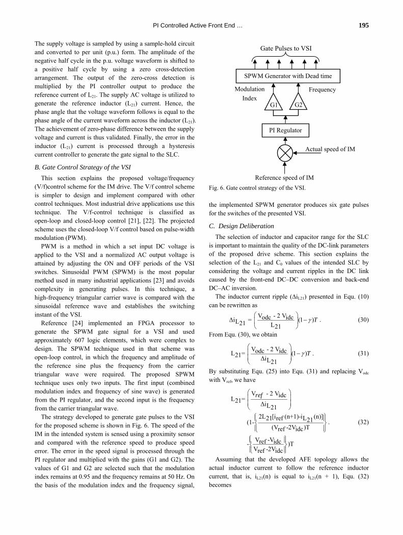
The strategy developed to generate gate pulses to the VSI for the proposed scheme is shown in Fig. 6. The speed of the IM in the intended system is sensed using a proximity sensor and compared with the reference speed to produce speed error. The error in the speed signal is processed through the PI regulator and multiplied with the gains (G1 and G2). The values of G1 and G2 are selected such that the modulation index remains at 0.95 and the frequency remains at 50 Hz. On the basis of the modulation index and the frequency signal,
Fig. 6. Gate control strategy of the VSI.
the implemented SPWM generator produces six gate pulses for the switches of the presented VSI.
C. Design Deliberation
The selection of inductor and capacitor range for the SLC is important to maintain the quality of the DC-link parameters of the proposed drive scheme. This section explains the selection of the L21 and C0 values of the intended SLC by considering the voltage and current ripples in the DC link caused by the front-end DC–DC conversion and back-end DC–AC inversion.
The inductor current ripple (∆iL21) presented in Equ. (10) can be rewritten as
V - 2 Vodc idcΔi = (1 )L21 L21T
. (30)
From Equ. (30), we obtain
V - 2 Vodc idcL = (1 )21 ΔiL21T
. (31)
By substituting Equ. (25) into Equ. (31) and replacing Vodc with Vref, we have
V - 2 Vidc L = 21 ΔiL21
2L [i (n+1)-i (n)]21 ref L21 (1-(V -2V )Tref idc
V -Vref idc - )TV -2Vref idc
ref
. (32)
Assuming that the developed AFE topology allows the actual inductor current to follow the reference inductor current, that is, iL21(n) is equal to iL21(n + 1), Equ. (32) becomes
Gate Pulses to VSI
Actual speed of IM
Reference speed of IM
PI Regulator
G2 G1
SPWM Generator with Dead time
Modulation
IndexFrequency
196 Journal of Power Electronics, Vol. 16, No. 1, January 2016
V - 2 V V -Vref idc ref idc L = (T- T)21 Δi V -2VL ref idc21
. (33)
On solving Equ. (33), the inductor L21 for the suggested SLC is expressed as
2V - 3 V V -Vref idc ref idc L = 121 Δi .f V -2VL s ref idc21
, (34)
where fs is the switching frequency of the SLC with the inverse of the time period T.
The DC-link capacitor Co filters the harmonic reflected back from the VSI of the recommended drive scheme and maintains ripple-free DC-link voltage. Hence, the selection of Co value is critical. This study concentrates only on the forward motoring mode, and the ripple caused by the reflected harmonic from the VSI is eliminated by injecting the ripple component with the same frequency as that of the throw back harmonic in the DC link. The injection of the ripple component is based on the knowledge of prediction control using an FPGA.
The DC-link ripple voltage (∆Vodc) is expressed as
I (1-γ) odcΔV = odc f .Cs o
. (35)
From Equ. (35), Co is expressed as
I (1-γ) odc C = o ΔV .fodc s
. (36)
Assuming that iL21(n) is equal to iL21(n + 1) and by substituting Equ. (25) into Equ. (36), we obtain
I V -Vodc ref idc C = 1-o ΔV .f V -2Vodc s ref idc
. (37)
The values of the inductor L21 and the capacitor Co highly depend on the switching frequency of the SLC and the DC-link voltage and current ripples. If the switching frequency of the SLC increases, then the values of L21 and Co are selected to be low. A high switching frequency results in electromagnetic interference (EMI). Hence, the selection of L21 and Co is made such that EMI should not exist.
IV. SIMULATION WORK AND RESULTS
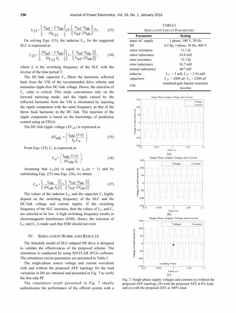
The Simulink model of SLC-adapted IM drive is designed to validate the effectiveness of the proposed scheme. The simulation is conducted by using MATLAB 2012a software. The simulation circuit parameters are presented in Table I.
The single-phase source voltage and current waveform with and without the proposed AFE topology for the load variations in IM are obtained and presented in Fig. 7 to verify the line-side PF.
The simulation result presented in Fig. 7 ideally authenticates the performance of the offered system with a
TABLE I SIMULATION CIRCUIT PARAMETERS
Parameter Rating input AC supply 1 phase, 100 V, 50 Hz IM 0.5 hp, 3 phase, 50 Hz, 400 V stator resistance 11.1 Ω stator inductance 18.8 mH rotor resistance 12.3 Ω rotor inductance 26.7 mH mutual inductance 467 mH inductor L11 = 3 mH, L21 = 2.56 mH capacitors C21 = 2000 µF, Co = 2200 µF
VSI insulated-gate bipolar transistor
inverter
0.9 0.95 1 1.05 1.1-150
-100
-50
0
50
100
150
Time (s)
Vol
tage
(V
) an
d C
urre
nt (
A)
Single Phase Supply Voltage and Current
Voltage Current
(a)
0.9 0.95 1 1.05 1.1-150
-100
-50
0
50
100
150
Time (s)
Vol
tage
(V
) an
d C
urre
nt (
A)
Single Phase Supply Voltage and Current
Voltage Current
(b)
0.9 0.95 1 1.05 1.1-150
-100
-50
0
50
100
150
Time (s)
Vol
tage
(V
) an
d C
urre
nt (
A)
Single Phase Supply Voltage and Current
Voltage Current
Loading Point
(c)
Fig. 7. Single-phase supply voltages and currents (a) without the proposed AFE topology, (b) with the proposed AFE at 0% load, and (c) with the proposed AFE at 100% load.
PI Controlled Active Front End … 197
1.9 1.92 1.94 1.96 1.98 20
5
10
15
Time (s)
Cur
rent
(A
)Reference and Actual Inductor Current
Actual CurrentReference Current
Fig. 8. Reference and actual inductor currents (iref and iL21).
0 0.5 1 1.5 20
100
200
300
400
500
Time (s)
Vol
tage
(V
)
DC Link Voltage
Actual VoltageReference Voltage
(a)
0 0.5 1 1.5 20
100
200
300
400
500
Time (s)
Vol
tage
(V
)
DC Link Voltage
Actual VoltageReference Voltage
Loading Point
(b)
Fig. 9. DC-link voltage for the reference 300 V (a) 0% load and (b) 100% load.
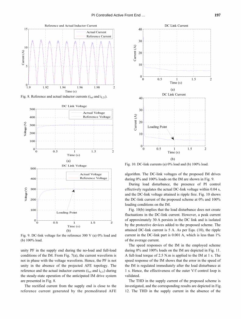
unity PF in the supply end during the no-load and full-load conditions of the IM. From Fig. 7(a), the current waveform is not in phase with the voltage waveform. Hence, the PF is not unity in the absence of the projected AFE topology. The reference and the actual inductor currents (iref and iL21) during the steady-state operation of the anticipated IM drive system are presented in Fig. 8.
The rectified current from the supply end is close to the reference current generated by the premeditated AFE
0 0.5 1 1.5 20
10
20
30
40
Time (s)
Cur
rent
(A
)
DC Link Current
(a)
0 0.5 1 1.5 20
10
20
30
40
Time (s)
Cur
rent
(A
)
DC Link Current
Loading Point
(b)
Fig. 10. DC-link currents (a) 0% load and (b) 100% load.
algorithm. The DC-link voltages of the proposed IM drives during 0% and 100% loads on the IM are shown in Fig. 9.
During load disturbance, the presence of PI control effectively regulates the actual DC-link voltage within 0.04 s, and the DC-link voltage attained is ripple free. Fig. 10 shows the DC-link current of the proposed scheme at 0% and 100% loading conditions on the IM.
Fig. 10(b) implies that the load disturbance does not create fluctuations in the DC-link current. However, a peak current of approximately 30 A persists in the DC link and is isolated by the protective devices added to the proposed scheme. The attained DC-link current is 5 A. As per Equ. (10), the ripple current in the DC-link part is 0.001 A, which is less than 1% of the average current.
The speed responses of the IM in the employed scheme during 0% and 100% loads on the IM are depicted in Fig. 11. A full-load torque of 2.5 N.m is applied to the IM at 1 s. The speed response of the IM shows that the error in the speed of the IM is regulated immediately after the load disturbance at 1 s. Hence, the effectiveness of the outer V/f control loop is validated.
The THD in the supply current of the proposed scheme is investigated, and the corresponding results are depicted in Fig. 12. The THD in the supply current in the absence of the
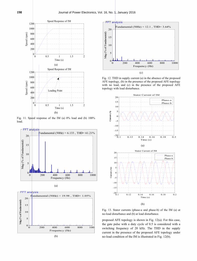
198 Journal of Power Electronics, Vol. 16, No. 1, January 2016
0 0.5 1 1.5 20
200
400
600
800
1000
1200
Time (s)
Spe
ed (
rpm
)
Speed Response of IM
(a)
0 0.5 1 1.5 20
200
400
600
800
1000
1200
Time (s)
Spe
ed (
rpm
)
Speed Response of IM
Loading Point
(b)
Fig. 11. Speed response of the IM (a) 0% load and (b) 100% load.
0 200 400 600 800 10000
5
10
15
20
Frequency (Hz)
Fundamental (50Hz) = 6.133 , THD= 61.21%
Mag
(%
of
Fun
dam
enta
l)
(a)
0 200 400 600 800 10000
5
10
15
20
Frequency (Hz)
Fundamental (50Hz) = 19.98 , THD= 1.05%
Mag
(%
of Fun
dam
enta
l)
(b)
0 200 400 600 800 10000
5
10
15
20
Frequency (Hz)
Fundamental (50Hz) = 12.1 , THD= 3.64%
Mag
(%
of
Fun
dam
enta
l)
(c)
Fig. 12. THD in supply current (a) in the absence of the proposed AFE topology, (b) in the presence of the proposed AFE topology with no load, and (c) in the presence of the proposed AFE topology with load disturbance.
0.1 0.12 0.14 0.16 0.18 0.2-20
-15
-10
-5
0
5
10
15
20
Time (s)
Cur
rent
(A)
Stator Current of IM
Phase-aPhase-b
(a)
0.1 0.12 0.14 0.16 0.18 0.2-20
-15
-10
-5
0
5
10
15
20
Time (s)
Cur
rent
(A
))
Stator Current of IM
Phase-aPhase-b
(b)
Fig. 13. Stator currents (phase-a and phase-b) of the IM (a) at no-load disturbance and (b) at load disturbance.
proposed AFE topology is shown in Fig. 12(a). For this case, the gate pulse with a duty cycle of 0.5 is considered with a switching frequency of 20 kHz. The THD in the supply current in the presence of the proposed AFE topology under no-load condition of the IM is illustrated in Fig. 12(b).
PI Controlled Active Front End … 199
Fig. 12(c) shows the THD in the supply current in the presence of the designed AFE topology under load disturbance of the IM. Fig. 12 indicates that the proposed AFE topology improves the THD in the supply current significantly. The stator current of the IM during the steady state and the run-up condition is presented in Fig. 13. The IM current in the developed drive scheme does not have any spikes. Hence, the insulation failure of stator winding is eliminated using the designed scheme.
V. EXPERIMENTAL WORK AND RESULTS
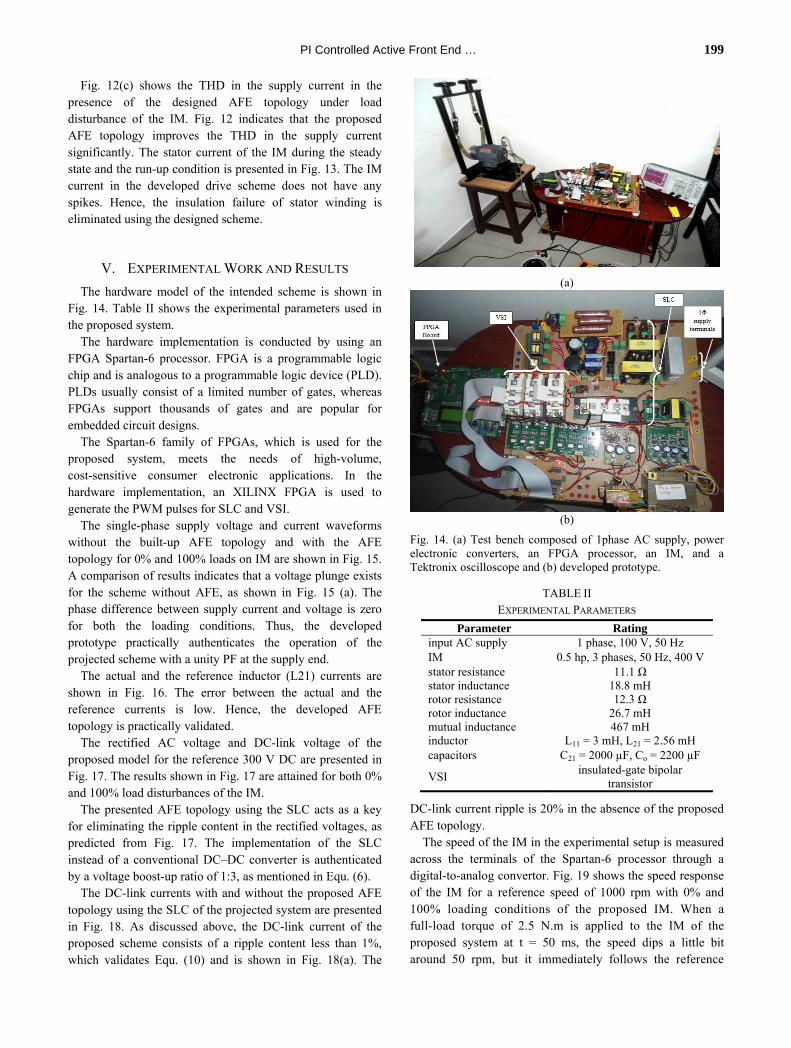
The hardware model of the intended scheme is shown in Fig. 14. Table II shows the experimental parameters used in the proposed system.
The hardware implementation is conducted by using an FPGA Spartan-6 processor. FPGA is a programmable logic chip and is analogous to a programmable logic device (PLD). PLDs usually consist of a limited number of gates, whereas FPGAs support thousands of gates and are popular for embedded circuit designs.
The Spartan-6 family of FPGAs, which is used for the proposed system, meets the needs of high-volume, cost-sensitive consumer electronic applications. In the hardware implementation, an XILINX FPGA is used to generate the PWM pulses for SLC and VSI.
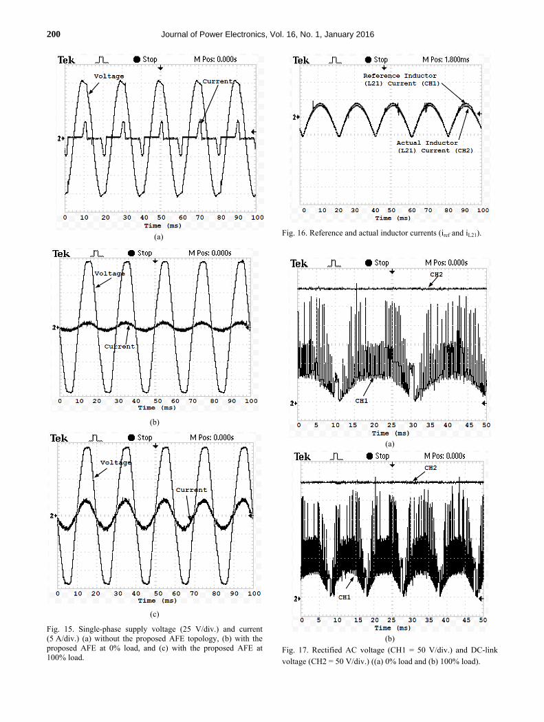
The single-phase supply voltage and current waveforms without the built-up AFE topology and with the AFE topology for 0% and 100% loads on IM are shown in Fig. 15. A comparison of results indicates that a voltage plunge exists for the scheme without AFE, as shown in Fig. 15 (a). The phase difference between supply current and voltage is zero for both the loading conditions. Thus, the developed prototype practically authenticates the operation of the projected scheme with a unity PF at the supply end.
The actual and the reference inductor (L21) currents are shown in Fig. 16. The error between the actual and the reference currents is low. Hence, the developed AFE topology is practically validated.
The rectified AC voltage and DC-link voltage of the proposed model for the reference 300 V DC are presented in Fig. 17. The results shown in Fig. 17 are attained for both 0% and 100% load disturbances of the IM.
The presented AFE topology using the SLC acts as a key for eliminating the ripple content in the rectified voltages, as predicted from Fig. 17. The implementation of the SLC instead of a conventional DC–DC converter is authenticated by a voltage boost-up ratio of 1:3, as mentioned in Equ. (6).
The DC-link currents with and without the proposed AFE topology using the SLC of the projected system are presented in Fig. 18. As discussed above, the DC-link current of the proposed scheme consists of a ripple content less than 1%, which validates Equ. (10) and is shown in Fig. 18(a). The
(a)
(b)
Fig. 14. (a) Test bench composed of 1phase AC supply, power electronic converters, an FPGA processor, an IM, and a Tektronix oscilloscope and (b) developed prototype.
TABLE II EXPERIMENTAL PARAMETERS
Parameter Rating input AC supply 1 phase, 100 V, 50 Hz IM 0.5 hp, 3 phases, 50 Hz, 400 Vstator resistance 11.1 Ω stator inductance 18.8 mH rotor resistance 12.3 Ω rotor inductance 26.7 mH mutual inductance 467 mH inductor L11 = 3 mH, L21 = 2.56 mH capacitors C21 = 2000 µF, Co = 2200 µF
VSI insulated-gate bipolar
transistor
DC-link current ripple is 20% in the absence of the proposed AFE topology.
The speed of the IM in the experimental setup is measured across the terminals of the Spartan-6 processor through a digital-to-analog convertor. Fig. 19 shows the speed response of the IM for a reference speed of 1000 rpm with 0% and 100% loading conditions of the proposed IM. When a full-load torque of 2.5 N.m is applied to the IM of the proposed system at t = 50 ms, the speed dips a little bit around 50 rpm, but it immediately follows the reference
200 Journal of Power Electronics, Vol. 16, No. 1, January 2016
(a)
(b)
(c)
Fig. 15. Single-phase supply voltage (25 V/div.) and current (5 A/div.) (a) without the proposed AFE topology, (b) with the proposed AFE at 0% load, and (c) with the proposed AFE at 100% load.
Fig. 16. Reference and actual inductor currents (iref and iL21).
(a)
(b)
Fig. 17. Rectified AC voltage (CH1 = 50 V/div.) and DC-link voltage (CH2 = 50 V/div.) ((a) 0% load and (b) 100% load).
PI Controlled Active Front End … 201
(a)
(b) Fig. 18. DC-link current (a) with the proposed AFE topology (CH2 = 1.25 A/div.) and (b) without the proposed AFE topology (CH1 = 1.25 A/div.). speed in a regulation period of 10 ms. The result of speed response verifies the feasibility of the closed-loop V/f control for the proposed model.
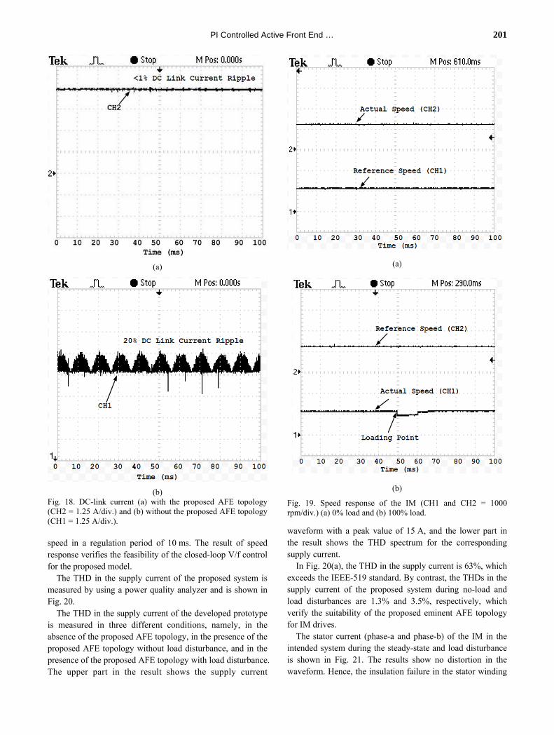
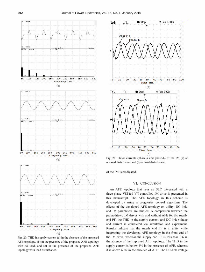
The THD in the supply current of the proposed system is measured by using a power quality analyzer and is shown in Fig. 20.
The THD in the supply current of the developed prototype is measured in three different conditions, namely, in the absence of the proposed AFE topology, in the presence of the proposed AFE topology without load disturbance, and in the presence of the proposed AFE topology with load disturbance. The upper part in the result shows the supply current
(a)
(b)
Fig. 19. Speed response of the IM (CH1 and CH2 = 1000 rpm/div.) (a) 0% load and (b) 100% load.
waveform with a peak value of 15 A, and the lower part in the result shows the THD spectrum for the corresponding supply current.
In Fig. 20(a), the THD in the supply current is 63%, which exceeds the IEEE-519 standard. By contrast, the THDs in the supply current of the proposed system during no-load and load disturbances are 1.3% and 3.5%, respectively, which verify the suitability of the proposed eminent AFE topology for IM drives.
The stator current (phase-a and phase-b) of the IM in the intended system during the steady-state and load disturbance is shown in Fig. 21. The results show no distortion in the waveform. Hence, the insulation failure in the stator winding
202 Journal of Power Electronics, Vol. 16, No. 1, January 2016
(a)
(b)
(c)
Fig. 20. THD in supply current (a) in the absence of the proposed AFE topology, (b) in the presence of the proposed AFE topology with no load, and (c) in the presence of the proposed AFE topology with load disturbance.
(a)
(b)
Fig. 21. Stator currents (phase-a and phase-b) of the IM (a) at no-load disturbance and (b) at load disturbance.
of the IM is eradicated.
VI. CONCLUSION
An AFE topology that uses an SLC integrated with a three-phase VSI-fed V/f controlled IM drive is presented in this manuscript. The AFE topology in this scheme is developed by using a prognostic control algorithm. The effects of the developed AFE topology on utility, DC link, and IM parameters are studied. A comparison between the premeditated IM drives with and without AFE for the supply end PF, the THD in the supply current, and DC-link voltage and current is conducted via simulation and experiment. Results indicate that the supply end PF is in unity while integrating the developed AFE topology in the front end of the IM drive, whereas the supply end PF is less than 0.6 in the absence of the improved AFE topology. The THD in the supply current is below 4% in the presence of AFE, whereas it is above 60% in the absence of AFE. The DC-link voltage

PI Controlled Active Front End … 203
and current ripples are eliminated with the SLC arrangement; this ability of the SLC is an advantage that makes it a suitable replacement for conventional DC–DC converters. The DC-link current ripple is less than 1% in the presence of the AFE-integrated SLC arrangement, whereas it is 20% in the absence of the arrangement. The IM response for load variations validates the suitability of the V/f control at the motor end for the intended scheme. The PI controller used in both ends is generally suitable for the proposed drive scheme in observing the error elimination in DC link and speed signals.
REFERENCES
[1] B.-R. Lin and C.-C. Chien, “Interleaved boost-flyback
converter with boundary conduction mode for power factor correction,” Journal of Power Electronics, Vol. 12, No. 5, pp. 708-714, Sep. 2012.
[2] J.-W. Shin, B.-C. Hyeon, and B.-H. Cho, “Digital control of a power factor correction boost rectifier using diode current sensing technique,” Journal of Power Electronics, Vol. 9, No. 6, pp.903-910, Nov. 2009.
[3] M. Lucanu, O. Ursaru, C. Aghion, and N. Lucanu, “Single-phase direct AC-AC boost converter,” Advances in Electrical and Computer Engineering, Vol. 14, No. 3, pp. 107-112, 2014.
[4] S. Sajeev and A. Mathew, “Novel cost effective induction motor drive with bridgeless PFC and four switch inverter,” in International Conference on Emerging Trends in Communication, Control, Signal Processing & Computing Applications(C2SPCA), pp. 1-6, Oct. 2013.
[5] R. Maheshwari, S. Munk-Nielsen, and K. Lu, “An active damping technique for small DC-link capacitor based drive system,” IEEE Trans. Ind. Informat., Vol. 9, No. 2, pp. 848-858, May 2013.
[6] F. Fleming, O. Vodyakho, C. S. Edrington, and M. Steurer, “Influence of DC-link fluctuations on three-phase induction motor drives,” in IEEE Vehicle Power and Propulsion Conference, pp.748-753, Sep. 2009.
[7] X. Du, L. Zhou, H. Lu, and H. M. Tai, “DC link active power filter for three-phase diode rectifier,” IEEE Trans. Ind. Electron., Vol. 59, No. 3, pp. 1430–1442, Mar. 2012.
[8] M. Hinkkanen and J. Luomi, “Induction motor drives equipped with diode rectifier and small DC-link capacitance,” IEEE Trans. Ind. Electron., Vol. 55, No. 1, pp. 312–320, Jan. 2008.
[9] K. Jalili, N. Weitendorf, and S. Bernet, “Behavior of PWM active front ends in the presence of parallel thyristor converters, IEEE Trans. Ind. Electron., Vol. 55, No. 3, pp.1035-1046, Mar. 2008
[10] N. Mendez-Gomez, O. Bousono, R. Castaneyra, and E. I. Ortiz-Rivera, “Development of a low cost induction motor drive system using a PVM, boost converter and three-phase inverter,” in IEEE 38th Photovoltaic Specialists Conference(PVSC), pp. 001348-001351, Jun. 2012.
[11] J. V. Caracas, G. C. Farias, L. F. Teixeira, and L. A. Ribeiro, “Implementation of a high-efficiency, high-lifetime, and low-cost converter for an autonomous photovoltaic water pumping system,” IEEE Trans. Ind. Appl., Vol. 50, No. 1, pp. 631 – 641, Jan. /Feb. 2014.
[12] F. L. Luo and H. Ye, Advanced Dc/DC Converters, CRC Press, Chapter 3, London, 2003.
[13] F. L. Luo and H. Ye, “Positive output super-lift converters,” IEEE Trans. Power Electron., Vol. 18, No. 1, pp.105-113, Jan. 2003.
[14] F. L. Luo, “Six self lift DC-DC converters, voltage lift technique,” IEEE Trans. Ind. Electron., Vol. 48, No. 6, pp. 1268-1272, Dec. 2001.
[15] K. R. Kumar and S. Jeevananthan, “PI control for positive output elementary super lift luo converter,” International Journal of Electrical, Computer, Energetic Electronic and Communication Engineering, Vol. 4, No. 3, pp. 544-549, 2010.
[16] L. Moran, J. Espinoza, M. Ortiz, J. Rodriguez, and J. Dixon, “Practical problems associated with the operation of ASDs based on active front end converters in power distribution systems,” in IEEE Industry Applications Conference, Vol. 4, pp. 2568-2572, Oct. 2004.
[17] F. L. Luo, “Luo-converters: A series of new DC-DC step-up (boost) conversion circuits,” in Proceeding of International Conference on Power Electronics and Drive Systems, Vol. 2, pp. 882-888, May 1997.
[18] P. Mattavelli, L. Rossetto, and G. Spiazzi, “Small signal analysis of DCDC converter with sliding mode control,” IEEE Trans. Power Electron., Vol. 12, No. 1, pp. 96-102, Jan. 1997.
[19] Y. Panov, J. Rajagopalan, and F. C. Lee, “Analysis and control design of N paralleled DC-DC converters with master-slave current sharing control,” in Proceeding of Applied Power Electronics Conference, pp. 436-442, 1997.
[20] P. Comines and N. Munro, “PID controllers: Recent tuning methods and design to specification,” in Proceeding of IEE Control Theory and Applications, Vol. 149, No. 1, pp. 46-53, Jan. 2002.
[21] M. H. V. Reddy and V. Jegathesan, “Open loop V/f control of induction motor based on hybrid PWM with reduced torque ripple,” in International Conference on Emerging Trends in Electrical and Computer Technology(ICETECT), pp. 331-336, Mar. 2011.
[22] C. S. Kamble, J. G. Chaudhari, and M. V. Aware, “Digital signal processor based V/F controlled induction motor drive,” in 3rd International Conference on Emerging Trends in Engineering and Technology(ICETET), pp. 345-349, Nov. 2010.
[23] A. M. Hava, R. J. Kerman, and T. A. Lipo “Carrier-based PWM-VSI over modulation strategies: Analysis, comparison and design,” IEEE Trans. Power Electron., Vol. 13, No. 4, pp. 674-689, Jul. 1998.
[24] A. Belkheiri, M. Belkheiri, S. Aoughellanet, and A. Rabhi, “FPGA implementation of configurable three-phase SPWM module,” in 2nd International Conference on Communications, Computing and Control Applications(CCCA), pp. 1-5, Dec. 2012.
Elangovan P. received his B.E. in Electrical and Electronics Engineering from Kamban Engineering College, Anna University, Tamil Nadu, India. He completed his M.E. in Power Electronics and Drives at Arunai Engineering College, Anna University, Tamil Nadu, India. He is presently pursuing his doctoral degree at the Anna University,
Tamil Nadu, India, and working as an assistant professor in the

204 Journal of Power Electronics, Vol. 16, No. 1, January 2016
Department of Electrical and Electronics Engineering at the S.K.P. Engineering College, Tamil Nadu, India. His research has been published in refereed international journals and conference. His research areas include power electronics, induction motor drives, and advanced converters.
Nalin Kant Mohanty obtained his M.Tech degree in Computer Applications in Industrial Drives from Visveswaraiah Technological University, Karnataka. He received his Ph.D. from Anna University, Tamil Nadu, India. He is a fellow and registered Chartered Engineer of the Institution of Engineers, India. He is a life
member of ISTE, ISCA, and SESI. He is presently working as a professor in the Department of Electrical and Electronics Engineering, Sri Venkateswara College of Engineering, Sriperumbudur, Tamilnadu, India. He has more than 15 years of teaching experience and has published 20 research papers in refereed international journals and conferences. His research areas include power electronics, electric motor drives and control, power quality, and renewable energy systems.