Embed Size (px)
Citation preview
The Desktop Muon Detector: A simple, physics-motivated
machine- and electronics-shop project for university students
S.N. Axani,∗ J.M. Conrad,† and C. Kirby‡
Physics Department, Massachusetts Institute of Technology, Cambridge, MA 02139
(Dated: August 26, 2016)
Abstract
This paper describes an undergraduate-level physics project that incorporates various aspects
of machine- and electronics-shop technical development. The desktop muon detector is a self-
contained apparatus that employs plastic scintillator as a detection medium and a silicon photo-
multiplier for light collection. These detectors can be battery powered and used in conjunction with
the provided software to make interesting physics measurements. The total cost of each counter is
approximately $100.
∗Electronic address: [email protected]†Electronic address: [email protected]‡Electronic address: [email protected]
1
arX
iv:1
606.
0119
6v3
[ph
ysic
s.ed
-ph]
25
Aug
201
6
I. INTRODUCTION
This paper describes an undergraduate project to produce a compact, self-contained
“desktop muon counter.” The muon detector is contained in a small light-tight enclosure
that measures 3”×3.25”×0.625”. This sits on a small electronics box that performs the data
acquisition and readout for the detector. The process of making the counters and the readout
will teach students valuable skills in the machine shop and in constructing and debugging
electronics. In the supplementary material [1], we provide the CAD drawings for machining,
the files for the printed circuit boards, the code required to program the micro-controller, and
the Python program to write the detector data to a computer. We can use the end product
as a single device (or in sets) to make interesting physics measurements. We present one
example measurement made at Fermi National Accelerator Laboratory (Fermilab). The
overall cost per counter is about $100. A cost break-down is supplied in the supplementary
material (PurchasingList.xml). An array of desktop muon counters is shown in Fig. 1.
This paper is inspired by class Phys. 063 at Swarthmore College, “Procedures in Exper-
imental Physics,” which was taken by one of the authors. This class introduces students to
“the techniques, materials, and the design of experimental apparatus; shop practice; printed
circuit design and construction” [2]. This desktop muon counter project combines all of
these aspects into a unified program and delivers a useful physics tool.
Similar devices are used in particle physics experiments to identify well-reconstructed
muon track samples for detector calibration. An existing example includes the “muon cubes”
that were installed in the MiniBooNE neutrino experiment at Fermilab [3]. These optically
isolated scintillator cubes were used in combination with a set of scintillation counters lo-
cated above the detector to accurately track and tag stopping muons. The original desktop
muon counter, produced at MIT, was a prototype for a sub-detector of PINGU, an upgrade
to the IceCube neutrino observatory, located at the South Pole [5]. In PINGU, optically
isolated cubes located throughout the detector could provide well-defined hits on a set of
muon tracks, allowing tests of track reconstruction. Thus, development of this detector is a
realistic exercise for students who intend to participate in particle and astrophysics physics
experiments in the future.
2
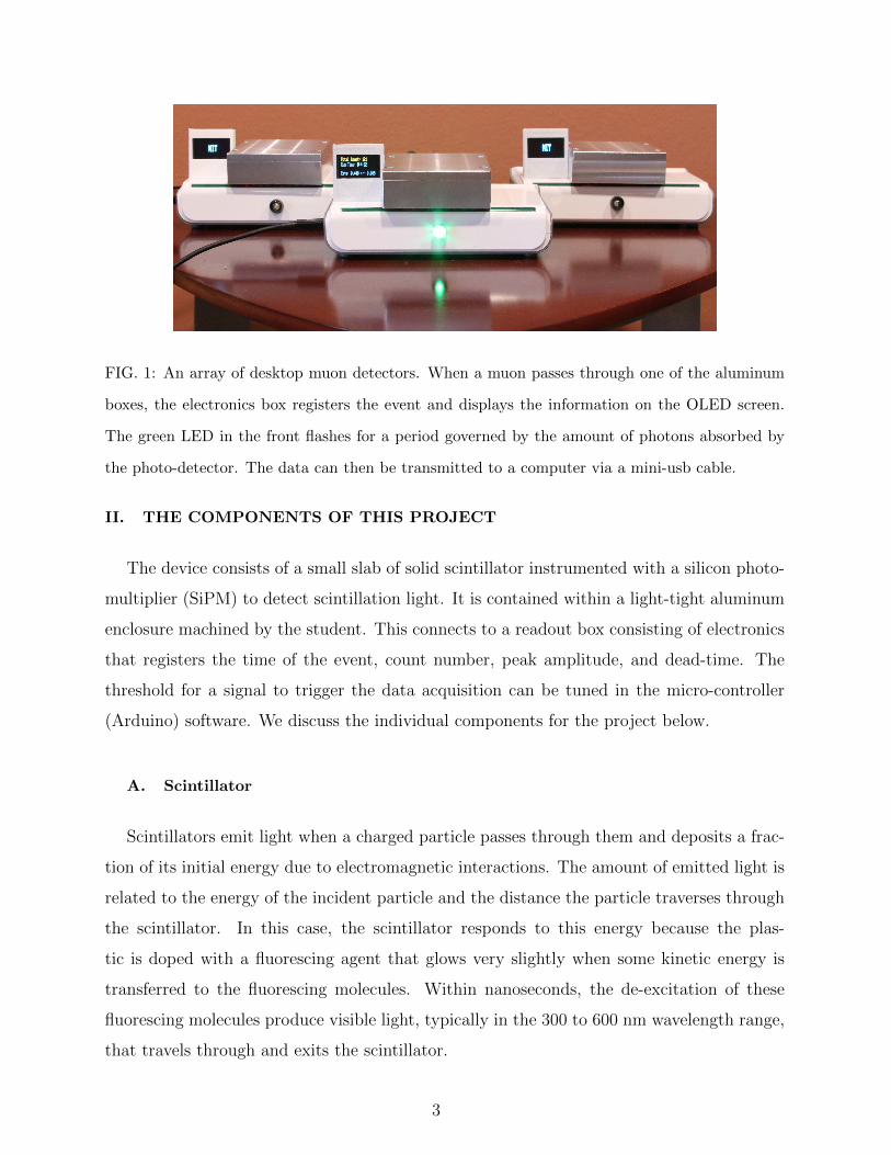
FIG. 1: An array of desktop muon detectors. When a muon passes through one of the aluminum
boxes, the electronics box registers the event and displays the information on the OLED screen.
The green LED in the front flashes for a period governed by the amount of photons absorbed by
the photo-detector. The data can then be transmitted to a computer via a mini-usb cable.
II. THE COMPONENTS OF THIS PROJECT
The device consists of a small slab of solid scintillator instrumented with a silicon photo-
multiplier (SiPM) to detect scintillation light. It is contained within a light-tight aluminum
enclosure machined by the student. This connects to a readout box consisting of electronics
that registers the time of the event, count number, peak amplitude, and dead-time. The
threshold for a signal to trigger the data acquisition can be tuned in the micro-controller
(Arduino) software. We discuss the individual components for the project below.
A. Scintillator
Scintillators emit light when a charged particle passes through them and deposits a frac-
tion of its initial energy due to electromagnetic interactions. The amount of emitted light is
related to the energy of the incident particle and the distance the particle traverses through
the scintillator. In this case, the scintillator responds to this energy because the plas-
tic is doped with a fluorescing agent that glows very slightly when some kinetic energy is
transferred to the fluorescing molecules. Within nanoseconds, the de-excitation of these
fluorescing molecules produce visible light, typically in the 300 to 600 nm wavelength range,
that travels through and exits the scintillator.
3
Scintillators comes in a number of forms other than solid plastic. For example there
are inorganic solid scintillators and liquid scintillators. However, we recommend plastic
scintillator for this project because it is inexpensive and easy to handle.
One can purchase new scintillator or use old scintillator paddles, as long as they are
sufficiently thick (we reconmend using a thickness of 10 mm). Because the detector is very
small, it is not a problem if the used scintillator has some minor damage. If your department
has no used scintillator available, we have found used paddles for sale for a very reasonable
price on eBay. New scintillator can be purchased if necessary from companies such as Saint
Gobain [6] or Eljen [7].
The scintillator slabs will be machined to size on a mill then polished by the students
using fine grit sandpaper and a polishing wheel. Polishing the scintillator improves the pho-
ton collection efficiency of the SiPM by increasing the optical transparency at the interface
between the SiPM and the plastic scintillator, and promotes total internal reflection off the
walls of the scintillator. We also wrap the plastic scintillator in reflective foil to increase the
number of photons reflected back towards the SiPM face. We use optical gel to match the
refractive indices of the plastic scintillator and the protective layer on the SiPMs photocath-
ode to increase efficiency. The SiPM is mounted on a printed circuit board (PCB), that is
fixed to the plastic scintillator by two screws.
B. Silicon Photomultipiers
The light emitted when a particle travels through the scintillator must be observed using
a light collection device. Traditionally, one attaches scintillator to photomultiplier tubes
(PMTs). These are large, require high voltages, and are expensive. In this case, we use a
single SiPM, since it requires only a low reverse bias voltage (positive voltage to the cathode,
negative voltage to the anode), has a peak sensitivity in the blue region where the majority
of scintillators emit most of their light, and is only a few millimeters thick with a cross
sectional area equal to the size of the photocathode. The low reverse bias means that we
can use an inexpensive DC-DC boost converter to power the circuit.
A SiPM consists of a large number of micro-cells each composed of silicon P-N junctions.
Electrons migrate into the P-side and holes migrate into the N-side. This creates a region
known as the “depletion region,” where the electrons and holes eliminate through recom-
4
bination. When a photon traverses the depleted region, it can deposit sufficient energy to
an electron in the valence band to move it to the conduction band, thereby creating a cur-
rent. Biasing the P-N junction increases the depletion region and creates an electric field
>5×10⁵ V/cm. When a charge carrier accelerates through this field, it can gain sufficient
kinetic energy to ionize the surrounding atoms through impact ionization. This creates an
avalanche of electron-hole pairs, which can have a gain as high as 1×10⁷. Thus a single
photon producing a single electron-hole pair can produce a very large, measurable signal.
SiPMs have a very high dark-noise rate. These are signals that occur randomly when ther-
modynamic processes in the silicon generate an electron-hole pair that proceeds to avalanche.
This signal is indistinguishable from that produced by a single photon. Therefore, it is es-
sential that a muon passing through the scintillator produces enough visible photons within
a short time period that the resulting signal is much larger than the noise background. Our
counter is designed with this goal in mind.
The detector described in this paper uses a 6×6 mm2 C-Series 60035-SMT SensL SiPM.
These SiPMs have a breakdown voltage of roughly 24.7 V and can add an over-voltage of up
to 5.0 V. The cost of SiPMs drops rapidly with the number that are purchased. Thus it is
most cost-effective for the department to buy SiPMs for a relatively large number of classes
at once, or to purchase them in conjunction with other classes or experiments. At the time
of writing this paper, the unit price of a bulk purchase of 100 SiPMs was below $50/SiPM.
This cost represents approximately half of the total cost of construction of the the desktop
muon counter.
C. Electronics components
There are two PCBs, each with surface mount components that the students will install.
The simplest of the two boards is used to mount the SiPM and provide bias filtering. This
PCB is mounted directly onto the plastic scintillator by means of two screws that maintain
pressure on the SiPM face to ensure good optical contact between the photocathode area and
the plastic scintillator. The second PCB contains the main electronics used to amplify and
shape the signal from the SiPM such that it can be measured by the micro-controller. It also
filters and regulates the voltages used in the detector. The amplification and shaping of the
waveform is accomplished using a dual, rail-to-rail input and output, operational-amplifiers
5
(op-amp) whose functions are described in detail in Sec. V. We use an inexpensive 16 MHz
Arduino Nano as a micro-controller and read the data out to a 0.96” OLED screen and
through a mini-USB cable to a computer. The code necessary to run the Arduino, as well
as a list of the required libraries (which all can be installed in the IDE), are supplied in the
supplementary material. We also provide a Python script to run on a computer to log the
data. Students are asked to design their own program to analyze the data.
D. The light-tight enclosure
The plastic scintillator and SiPM circuit are mounted in a light-tight aluminum enclosure.
The enclosure not only keeps the light from the scintillator in, it also protects from photons
from the outside environment. This prevents environmental noise from producing false
signals. However, the metal box has to be penetrated to bring in the voltage required to
run the SiPM and output the signal from the SiPM. This is done using connectors that are
light-tight.
E. Cables and electronics case
The signal from the SiPM is transmitted out of the light-tight enclosure to an electronics
case via an 8” BNC cable. Here the students are asked to manufacture their own BNC cable
and check the continuity of their connections. Since BNC cables are so prevalent in physics
labs due to their robust coaxial design and RF shielding characteristics, understanding how
to make your own or repair a noisy cable is an important skill. We use a simple 2.1×5.5 mm
DC cable to power the SiPM circuit.
The electronics case houses the main PCB. There are many design options for the electron-
ics case. It is crucial to make sure that the electronics can be securely mounted with enough
room to allow for the final soldering of connections. There should be at least 3”×4”×1”
internal volume to accommodate the electronics. In the designs shown in Fig. 1, we use a
re-purposed Ethernet switching cases.
6
III. MANUFACTURING THE COMPONENTS
This section describes the machining, 3D-printing, and PCB board manufacturing re-
quired for each component. Further technical material (CAD drawings, files, programs, and
documentation) of the manufacturing can be found in the supplementary material and will
be referenced as needed.
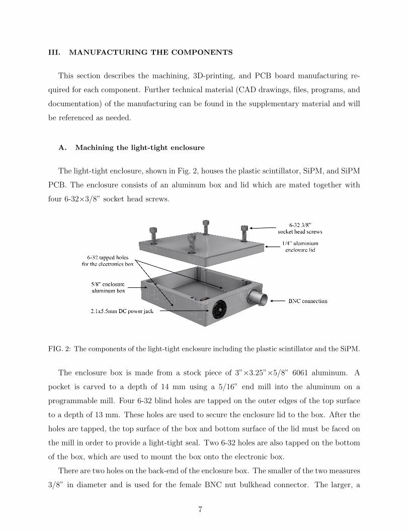
A. Machining the light-tight enclosure
The light-tight enclosure, shown in Fig. 2, houses the plastic scintillator, SiPM, and SiPM
PCB. The enclosure consists of an aluminum box and lid which are mated together with
four 6-32×3/8” socket head screws.
FIG. 2: The components of the light-tight enclosure including the plastic scintillator and the SiPM.
The enclosure box is made from a stock piece of 3”×3.25”×5/8” 6061 aluminum. A
pocket is carved to a depth of 14 mm using a 5/16” end mill into the aluminum on a
programmable mill. Four 6-32 blind holes are tapped on the outer edges of the top surface
to a depth of 13 mm. These holes are used to secure the enclosure lid to the box. After the
holes are tapped, the top surface of the box and bottom surface of the lid must be faced on
the mill in order to provide a light-tight seal. Two 6-32 holes are also tapped on the bottom
of the box, which are used to mount the box onto the electronic box.
There are two holes on the back-end of the enclosure box. The smaller of the two measures
3/8” in diameter and is used for the female BNC nut bulkhead connector. The larger, a
7
2.1×5.5 mm DC power jack used to supply the 29.5 V required to power the SiPM circuit.
The DC power jack is held in place with a layer of black epoxy. The epoxy is not ideal for
a light-tight enclosure, but is found to be sufficient for our purposes.
The enclosure lid is made from a stock piece of 3”×3.25”×1/4” 6061 aluminum plate.
The bottom side must also be faced to ensure the box is light-tight when closed. Four
countersunk through holes for the four 6-32 socket head screws are drilled on the outer edge
to line up with the four holes in the enclosure box.
The CAD drawings (Machining/LightTightEnclosureBox.pdf, Machin-
ing/LightTightEnclosureLid.pdf) and files for programming the mill (Machin-
ing/LightTightEnclosureBoxCNC.stp) are provided in the supplementary material.
We recommend that the students use the mill for the entire manufacturing process of this
component. This will help ensure that the holes are properly aligned and the edges are
square. Further, after the enclosure is assembled, all six faces can be faced to provide a
smooth, polished final finish.
B. Polishing the plastic scintillator
The plastic scintillator can be cut to the approximate size using a band saw and then
faced on a mill using a 4-flute, 3/4” endmill. Our final size measured 47×47×10 mm3. The
faces that were already transparent did not need to be machined. We found that a very
shallow final pass on the mill provided a very smooth, although visibly murky, finish.
The optical transmission through the milled surfaces can be improved using fine grit
sandpaper and a polishing wheel. We recommend working on a smooth, hard surface, such
as a granite counter or metal plate, with grits ranging from 1000 to 2500+. A bit of water
should be added to the top of the sandpaper to help cool the scintillator while sanding.
After a finishing pass on the fine grit sandpaper, the remaining blemishes can be removed
on a polishing wheel. It is important not to apply too much pressure on the polishing wheel
as the face of the plastic scintillator can be easily damaged by the heat generated from the
friction.
Two 3/64” holes, separated by 44 mm, are drilled to a depth of 0.25” on one of the faces
of the plastic scintillator to mount the SiPM PCB. When drilling into plastic, one should
maintain a low rpm and use a pecking motion to remove built up pieces of plastic. This will
8
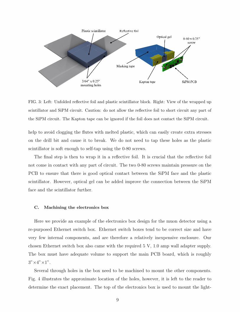
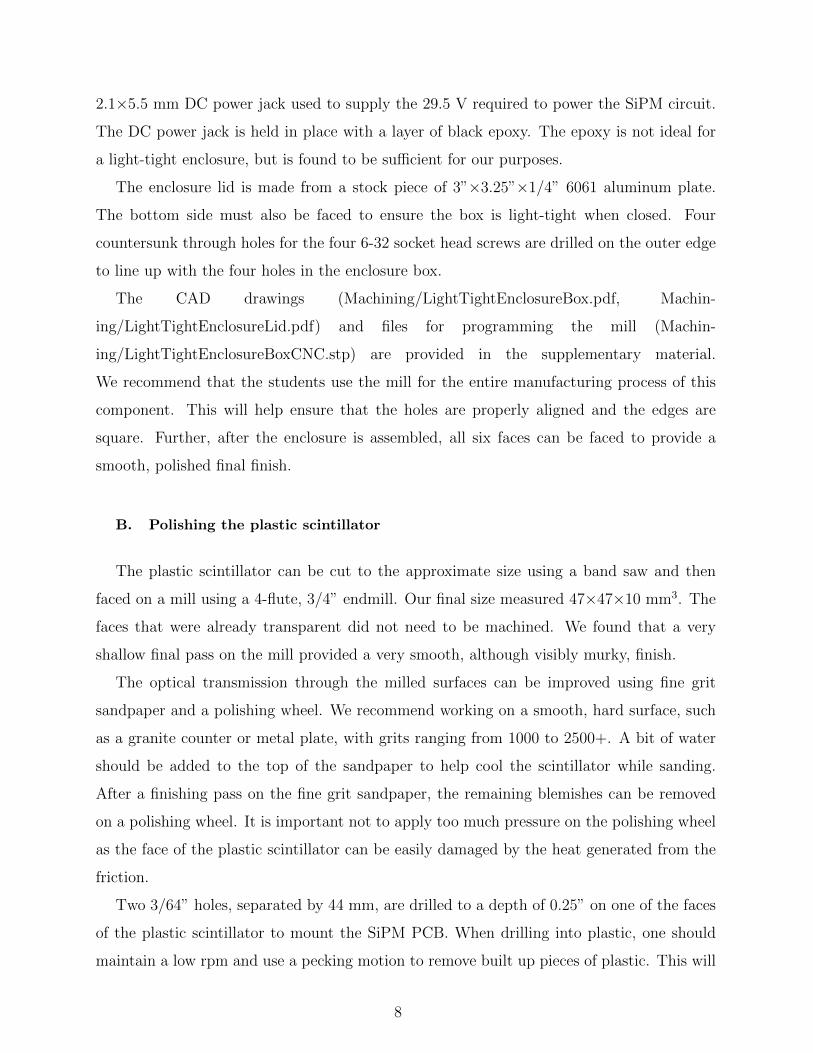
FIG. 3: Left: Unfolded reflective foil and plastic scintillator block. Right: View of the wrapped up
scintillator and SiPM circuit. Caution: do not allow the reflective foil to short circuit any part of
the SiPM circuit. The Kapton tape can be ignored if the foil does not contact the SiPM circuit.
help to avoid clogging the flutes with melted plastic, which can easily create extra stresses
on the drill bit and cause it to break. We do not need to tap these holes as the plastic
scintillator is soft enough to self-tap using the 0-80 screws.
The final step is then to wrap it in a reflective foil. It is crucial that the reflective foil
not come in contact with any part of circuit. The two 0-80 screws maintain pressure on the
PCB to ensure that there is good optical contact between the SiPM face and the plastic
scintillator. However, optical gel can be added improve the connection between the SiPM
face and the scintillator further.
C. Machining the electronics box
Here we provide an example of the electronics box design for the muon detector using a
re-purposed Ethernet switch box. Ethernet switch boxes tend to be correct size and have
very few internal components, and are therefore a relatively inexpensive enclosure. Our
chosen Ethernet switch box also came with the required 5 V, 1.0 amp wall adapter supply.
The box must have adequate volume to support the main PCB board, which is roughly
3”×4”×1”.
Several through holes in the box need to be machined to mount the other components.
Fig. 4 illustrates the approximate location of the holes, however, it is left to the reader to
determine the exact placement. The top of the electronics box is used to mount the light-
9
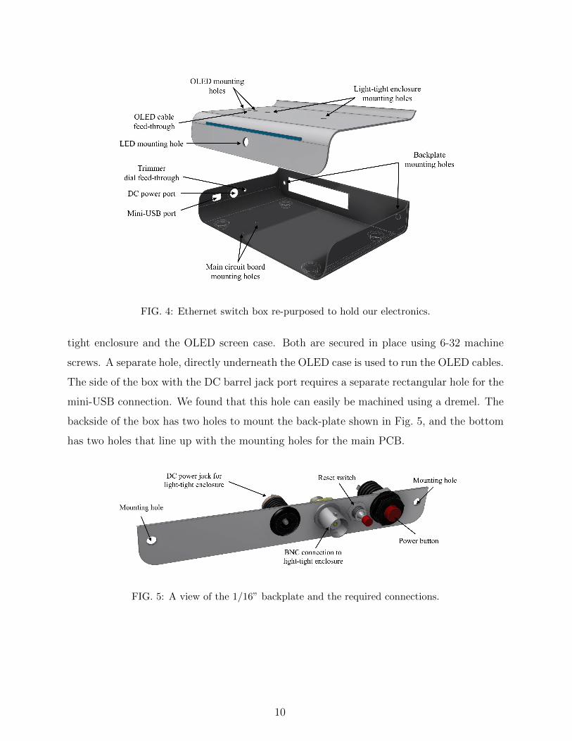
FIG. 4: Ethernet switch box re-purposed to hold our electronics.
tight enclosure and the OLED screen case. Both are secured in place using 6-32 machine
screws. A separate hole, directly underneath the OLED case is used to run the OLED cables.
The side of the box with the DC barrel jack port requires a separate rectangular hole for the
mini-USB connection. We found that this hole can easily be machined using a dremel. The
backside of the box has two holes to mount the back-plate shown in Fig. 5, and the bottom
has two holes that line up with the mounting holes for the main PCB.
FIG. 5: A view of the 1/16” backplate and the required connections.
10
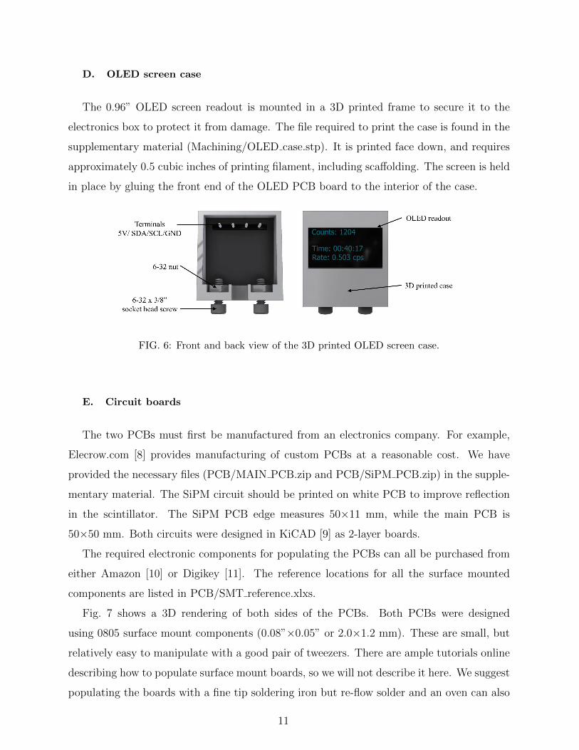
D. OLED screen case
The 0.96” OLED screen readout is mounted in a 3D printed frame to secure it to the
electronics box to protect it from damage. The file required to print the case is found in the
supplementary material (Machining/OLED case.stp). It is printed face down, and requires
approximately 0.5 cubic inches of printing filament, including scaffolding. The screen is held
in place by gluing the front end of the OLED PCB board to the interior of the case.
FIG. 6: Front and back view of the 3D printed OLED screen case.
E. Circuit boards
The two PCBs must first be manufactured from an electronics company. For example,
Elecrow.com [8] provides manufacturing of custom PCBs at a reasonable cost. We have
provided the necessary files (PCB/MAIN PCB.zip and PCB/SiPM PCB.zip) in the supple-
mentary material. The SiPM circuit should be printed on white PCB to improve reflection
in the scintillator. The SiPM PCB edge measures 50×11 mm, while the main PCB is
50×50 mm. Both circuits were designed in KiCAD [9] as 2-layer boards.
The required electronic components for populating the PCBs can all be purchased from
either Amazon [10] or Digikey [11]. The reference locations for all the surface mounted
components are listed in PCB/SMT reference.xlxs.
Fig. 7 shows a 3D rendering of both sides of the PCBs. Both PCBs were designed
using 0805 surface mount components (0.08”×0.05” or 2.0×1.2 mm). These are small, but
relatively easy to manipulate with a good pair of tweezers. There are ample tutorials online
describing how to populate surface mount boards, so we will not describe it here. We suggest
populating the boards with a fine tip soldering iron but re-flow solder and an oven can also
11
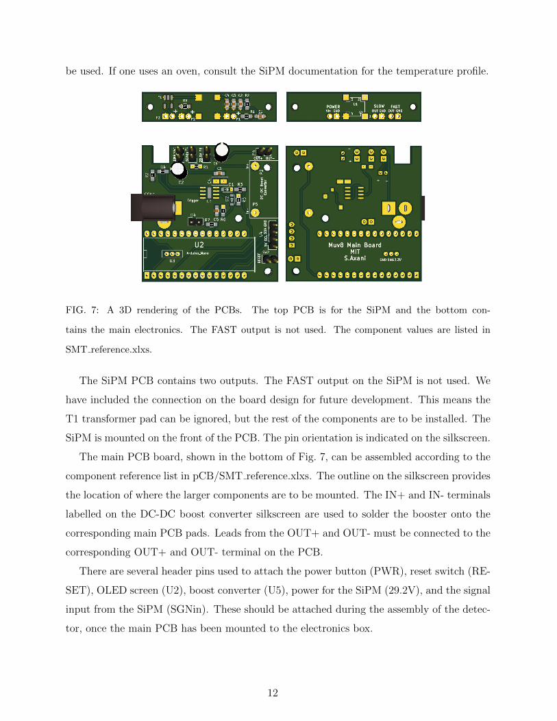
be used. If one uses an oven, consult the SiPM documentation for the temperature profile.
FIG. 7: A 3D rendering of the PCBs. The top PCB is for the SiPM and the bottom con-
tains the main electronics. The FAST output is not used. The component values are listed in
SMT reference.xlxs.
The SiPM PCB contains two outputs. The FAST output on the SiPM is not used. We
have included the connection on the board design for future development. This means the
T1 transformer pad can be ignored, but the rest of the components are to be installed. The
SiPM is mounted on the front of the PCB. The pin orientation is indicated on the silkscreen.
The main PCB board, shown in the bottom of Fig. 7, can be assembled according to the
component reference list in pCB/SMT reference.xlxs. The outline on the silkscreen provides
the location of where the larger components are to be mounted. The IN+ and IN- terminals
labelled on the DC-DC boost converter silkscreen are used to solder the booster onto the
corresponding main PCB pads. Leads from the OUT+ and OUT- must be connected to the
corresponding OUT+ and OUT- terminal on the PCB.
There are several header pins used to attach the power button (PWR), reset switch (RE-
SET), OLED screen (U2), boost converter (U5), power for the SiPM (29.2V), and the signal
input from the SiPM (SGNin). These should be attached during the assembly of the detec-
tor, once the main PCB has been mounted to the electronics box.
12
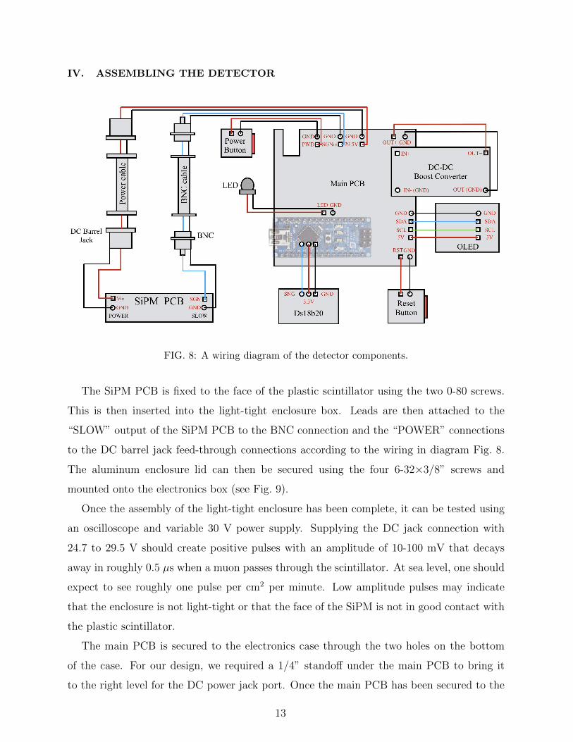
IV. ASSEMBLING THE DETECTOR
FIG. 8: A wiring diagram of the detector components.
The SiPM PCB is fixed to the face of the plastic scintillator using the two 0-80 screws.
This is then inserted into the light-tight enclosure box. Leads are then attached to the
“SLOW” output of the SiPM PCB to the BNC connection and the “POWER” connections
to the DC barrel jack feed-through connections according to the wiring in diagram Fig. 8.
The aluminum enclosure lid can then be secured using the four 6-32×3/8” screws and
mounted onto the electronics box (see Fig. 9).
Once the assembly of the light-tight enclosure has been complete, it can be tested using
an oscilloscope and variable 30 V power supply. Supplying the DC jack connection with
24.7 to 29.5 V should create positive pulses with an amplitude of 10-100 mV that decays
away in roughly 0.5 µs when a muon passes through the scintillator. At sea level, one should
expect to see roughly one pulse per cm2 per minute. Low amplitude pulses may indicate
that the enclosure is not light-tight or that the face of the SiPM is not in good contact with
the plastic scintillator.
The main PCB is secured to the electronics case through the two holes on the bottom
of the case. For our design, we required a 1/4” standoff under the main PCB to bring it
to the right level for the DC power jack port. Once the main PCB has been secured to the
13
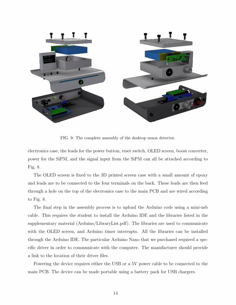
FIG. 9: The complete assembly of the desktop muon detector.
electronics case, the leads for the power button, reset switch, OLED screen, boost converter,
power for the SiPM, and the signal input from the SiPM can all be attached according to
Fig. 8.
The OLED screen is fixed to the 3D printed screen case with a small amount of epoxy
and leads are to be connected to the four terminals on the back. These leads are then feed
through a hole on the top of the electronics case to the main PCB and are wired according
to Fig. 8.
The final step in the assembly process is to upload the Arduino code using a mini-usb
cable. This requires the student to install the Arduino IDE and the libraries listed in the
supplementary material (Arduino/LibraryList.pdf). The libraries are used to communicate
with the OLED screen, and Arduino timer interrupts. All the libraries can be installed
through the Arduino IDE. The particular Arduino Nano that we purchased required a spe-
cific driver in order to communicate with the computer. The manufacturer should provide
a link to the location of their driver files.
Powering the device requires either the USB or a 5V power cable to be connected to the
main PCB. The device can be made portable using a battery pack for USB chargers.
14
V. THE ELECTRONICS CIRCUITRY
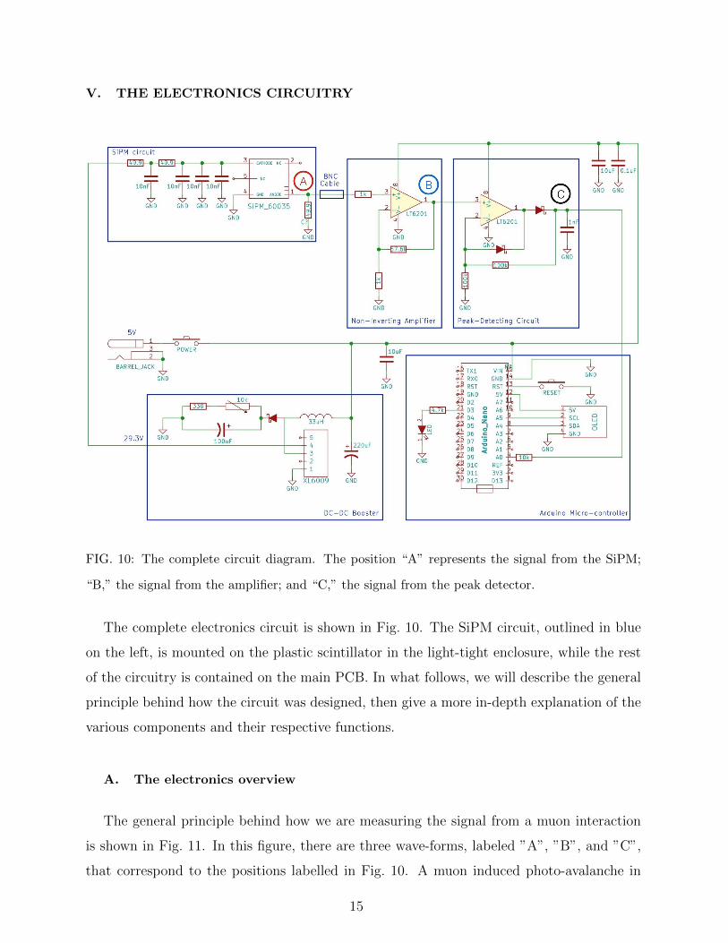
FIG. 10: The complete circuit diagram. The position “A” represents the signal from the SiPM;
“B,” the signal from the amplifier; and “C,” the signal from the peak detector.
The complete electronics circuit is shown in Fig. 10. The SiPM circuit, outlined in blue
on the left, is mounted on the plastic scintillator in the light-tight enclosure, while the rest
of the circuitry is contained on the main PCB. In what follows, we will describe the general
principle behind how the circuit was designed, then give a more in-depth explanation of the
various components and their respective functions.
A. The electronics overview
The general principle behind how we are measuring the signal from a muon interaction
is shown in Fig. 11. In this figure, there are three wave-forms, labeled ”A”, ”B”, and ”C”,
that correspond to the positions labelled in Fig. 10. A muon induced photo-avalanche in
15
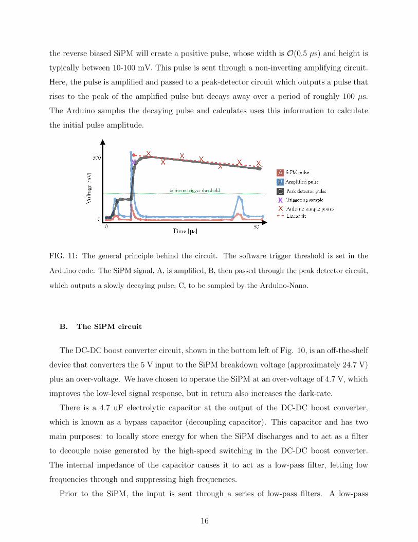
the reverse biased SiPM will create a positive pulse, whose width is O(0.5 µs) and height is
typically between 10-100 mV. This pulse is sent through a non-inverting amplifying circuit.
Here, the pulse is amplified and passed to a peak-detector circuit which outputs a pulse that
rises to the peak of the amplified pulse but decays away over a period of roughly 100 µs.
The Arduino samples the decaying pulse and calculates uses this information to calculate
the initial pulse amplitude.
FIG. 11: The general principle behind the circuit. The software trigger threshold is set in the
Arduino code. The SiPM signal, A, is amplified, B, then passed through the peak detector circuit,
which outputs a slowly decaying pulse, C, to be sampled by the Arduino-Nano.
B. The SiPM circuit
The DC-DC boost converter circuit, shown in the bottom left of Fig. 10, is an off-the-shelf
device that converters the 5 V input to the SiPM breakdown voltage (approximately 24.7 V)
plus an over-voltage. We have chosen to operate the SiPM at an over-voltage of 4.7 V, which
improves the low-level signal response, but in return also increases the dark-rate.
There is a 4.7 uF electrolytic capacitor at the output of the DC-DC boost converter,
which is known as a bypass capacitor (decoupling capacitor). This capacitor and has two
main purposes: to locally store energy for when the SiPM discharges and to act as a filter
to decouple noise generated by the high-speed switching in the DC-DC boost converter.
The internal impedance of the capacitor causes it to act as a low-pass filter, letting low
frequencies through and suppressing high frequencies.
Prior to the SiPM, the input is sent through a series of low-pass filters. A low-pass
16
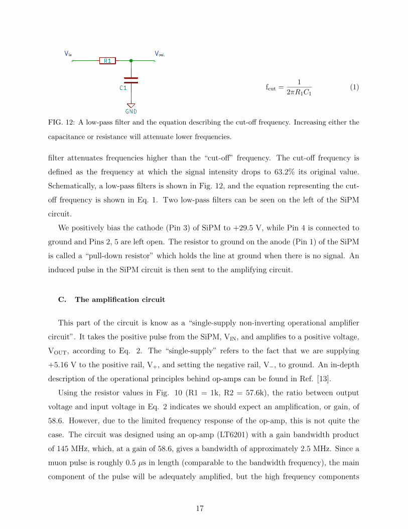
fcut =1
2πR1C1(1)
FIG. 12: A low-pass filter and the equation describing the cut-off frequency. Increasing either the
capacitance or resistance will attenuate lower frequencies.
filter attenuates frequencies higher than the “cut-off” frequency. The cut-off frequency is
defined as the frequency at which the signal intensity drops to 63.2% its original value.
Schematically, a low-pass filters is shown in Fig. 12, and the equation representing the cut-
off frequency is shown in Eq. 1. Two low-pass filters can be seen on the left of the SiPM
circuit.
We positively bias the cathode (Pin 3) of SiPM to +29.5 V, while Pin 4 is connected to
ground and Pins 2, 5 are left open. The resistor to ground on the anode (Pin 1) of the SiPM
is called a “pull-down resistor” which holds the line at ground when there is no signal. An
induced pulse in the SiPM circuit is then sent to the amplifying circuit.
C. The amplification circuit
This part of the circuit is know as a “single-supply non-inverting operational amplifier
circuit”. It takes the positive pulse from the SiPM, VIN, and amplifies to a positive voltage,
VOUT, according to Eq. 2. The “single-supply” refers to the fact that we are supplying
+5.16 V to the positive rail, V+, and setting the negative rail, V−, to ground. An in-depth
description of the operational principles behind op-amps can be found in Ref. [13].
Using the resistor values in Fig. 10 (R1 = 1k, R2 = 57.6k), the ratio between output
voltage and input voltage in Eq. 2 indicates we should expect an amplification, or gain, of
58.6. However, due to the limited frequency response of the op-amp, this is not quite the
case. The circuit was designed using an op-amp (LT6201) with a gain bandwidth product
of 145 MHz, which, at a gain of 58.6, gives a bandwidth of approximately 2.5 MHz. Since a
muon pulse is roughly 0.5 µs in length (comparable to the bandwidth frequency), the main
component of the pulse will be adequately amplified, but the high frequency components
17
Vout = Vin(1 +R2
R1) (2)
FIG. 13: Single supply non-inverting op-amp circuit and associated gain equation.
(namely the fast rise time and peak of the pulse) will be attenuated. Since the Arduino has
a limited temporal resolution (several microseconds), loosing information on the nanosecond
rise time is inconsequential.
D. The peak detector circuit
The purpose of the peak detector circuit is to output the highest point of the input
waveform to allow the Arduino sufficient time to measure it, then decay away and wait
for the next pulse. Since the SiPM has a dark-rate of approximately 100 kHz/mm2 at an
over-voltage of 4.7 V, the output of the peak detector output will not rest at ground, but
instead actually rest at a ”noise-floor”.
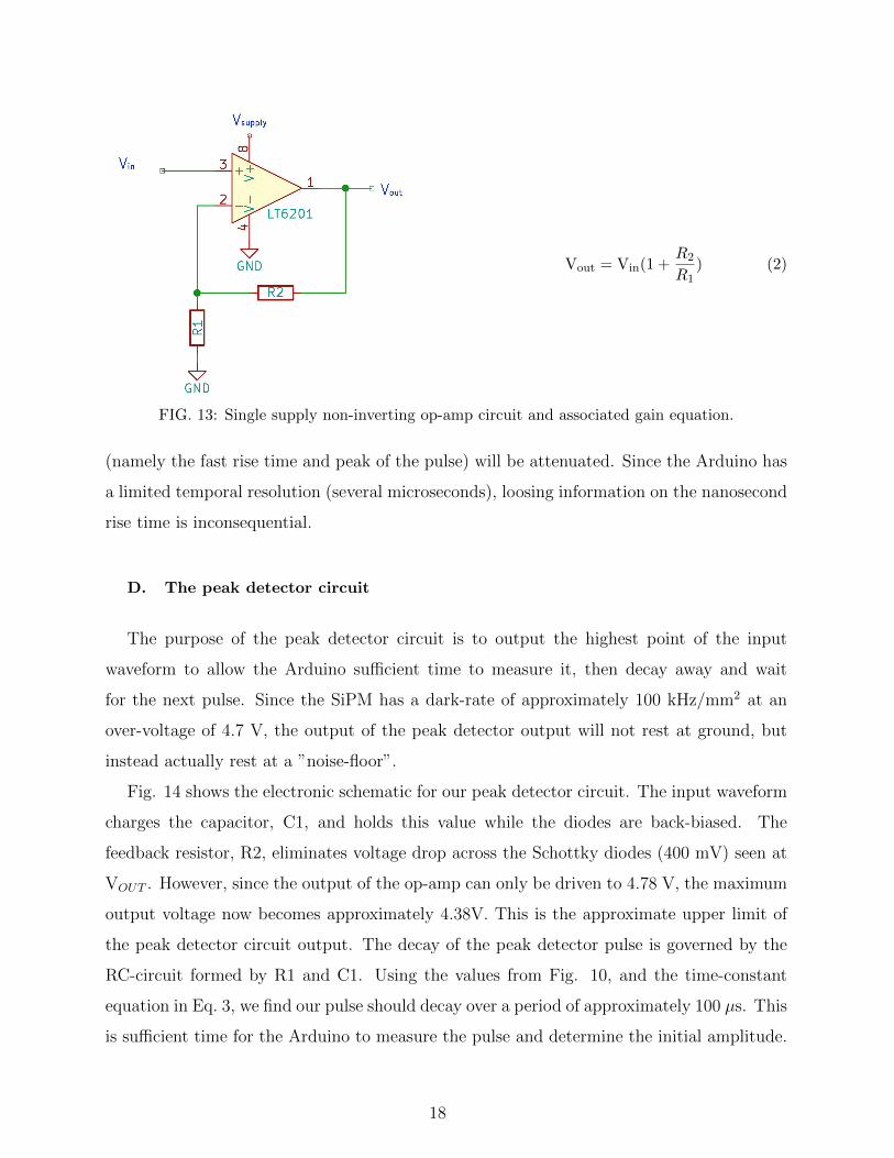
Fig. 14 shows the electronic schematic for our peak detector circuit. The input waveform
charges the capacitor, C1, and holds this value while the diodes are back-biased. The
feedback resistor, R2, eliminates voltage drop across the Schottky diodes (400 mV) seen at
VOUT . However, since the output of the op-amp can only be driven to 4.78 V, the maximum
output voltage now becomes approximately 4.38V. This is the approximate upper limit of
the peak detector circuit output. The decay of the peak detector pulse is governed by the
RC-circuit formed by R1 and C1. Using the values from Fig. 10, and the time-constant
equation in Eq. 3, we find our pulse should decay over a period of approximately 100 µs. This
is sufficient time for the Arduino to measure the pulse and determine the initial amplitude.
18
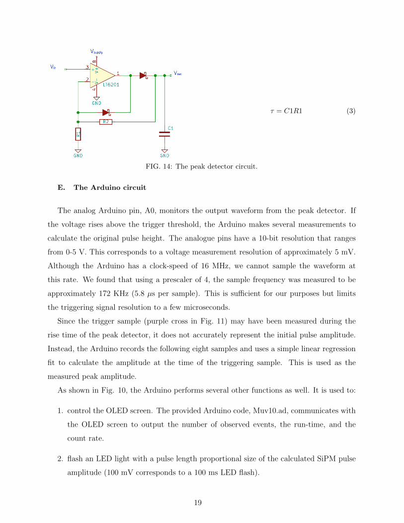
τ = C1R1 (3)
FIG. 14: The peak detector circuit.
E. The Arduino circuit
The analog Arduino pin, A0, monitors the output waveform from the peak detector. If
the voltage rises above the trigger threshold, the Arduino makes several measurements to
calculate the original pulse height. The analogue pins have a 10-bit resolution that ranges
from 0-5 V. This corresponds to a voltage measurement resolution of approximately 5 mV.
Although the Arduino has a clock-speed of 16 MHz, we cannot sample the waveform at
this rate. We found that using a prescaler of 4, the sample frequency was measured to be
approximately 172 KHz (5.8 µs per sample). This is sufficient for our purposes but limits
the triggering signal resolution to a few microseconds.
Since the trigger sample (purple cross in Fig. 11) may have been measured during the
rise time of the peak detector, it does not accurately represent the initial pulse amplitude.
Instead, the Arduino records the following eight samples and uses a simple linear regression
fit to calculate the amplitude at the time of the triggering sample. This is used as the
measured peak amplitude.
As shown in Fig. 10, the Arduino performs several other functions as well. It is used to:
1. control the OLED screen. The provided Arduino code, Muv10.ad, communicates with
the OLED screen to output the number of observed events, the run-time, and the
count rate.
2. flash an LED light with a pulse length proportional size of the calculated SiPM pulse
amplitude (100 mV corresponds to a 100 ms LED flash).
19
3. monitor the detector dead-time. While the detector is performing all the tasks in
the previous bullets, it monitors the dead-time so that an accurate muon rate can
be determined. The main sources of dead-time is updating the OLED screen. Each
update, which happens every second, takes approximately 35 ms. The next largest
source of dead-time is outputting the data through the serial connection, this takes
17.7 ms on average.
4. communicate with a computer via the mini-USB terminal. This is used to record
data directly to a computer. time-stamp of the event given by Python, event number,
time stamp of the event from the Arduino, event number, peak detector amplitude,
calculated SiPM pulse amplitude, and dead-time.
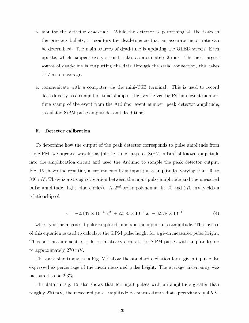
F. Detector calibration
To determine how the output of the peak detector corresponds to pulse amplitude from
the SiPM, we injected waveforms (of the same shape as SiPM pulses) of known amplitude
into the amplification circuit and used the Arduino to sample the peak detector output.
Fig. 15 shows the resulting measurements from input pulse amplitudes varying from 20 to
340 mV. There is a strong correlation between the input pulse amplitude and the measured
pulse amplitude (light blue circles). A 2nd-order polynomial fit 20 and 270 mV yields a
relationship of:
y = −2.132× 10−5 x2 + 2.366× 10⁻² x − 3.378× 10⁻¹ (4)
where y is the measured pulse amplitude and x is the input pulse amplitude. The inverse
of this equation is used to calculate the SiPM pulse height for a given measured pulse height.
Thus our measurements should be relatively accurate for SiPM pulses with amplitudes up
to approximately 270 mV.
The dark blue triangles in Fig. V F show the standard deviation for a given input pulse
expressed as percentage of the mean measured pulse height. The average uncertainty was
measured to be 2.3%.
The data in Fig. 15 also shows that for input pulses with an amplitude greater than
roughly 270 mV, the measured pulse amplitude becomes saturated at approximately 4.5 V.
20
FIG. 15: Calibration data for the complete circuit. There are 200 samples per input pulse amplitude
(light blue circles). The measurement are semi-opaque to show the relative distribution. The
standard deviation of a measurement for a given input pulse is shown as a percentage as dark blue
triangles.
This is due to the limited voltage range on the op-amp combined with the voltage drop
across the diode in the peak detector circuit. While pulses with initial amplitudes greater
than 270 mV are observed, they are relatively rare.
VI. LEARN ABOUT COSMIC RAY MUONS
The desktop muon counter is triggering on muons that are produced when high energy
astrophysical particles, called cosmic rays, collide with the Earth’s atmosphere producing
particles that decay to muons. In his 1950 Nobel Lecture, C.F. Powell described cosmic rays
as a “thin rain of charged particles” [14]. Most cosmic rays are produced in our galaxy and
are nuclei expelled in supernova explosions. About 90% of cosmic rays are protons, 9% are
helium nuclei, and the remaining 1% are heavier nuclei. When the cosmic rays hit the nuclei
of the atmosphere, a shower of particles are produced including pions and kaons. These
are the progenitors of the muons. Ref. [15–17] are three classic works by physicist Bruno
Rossi about cosmic rays that students may be assigned to read. The origin and content of
cosmic rays remains a hot topic of study today, with major conferences devoted to the latest
results [18]. A useful resource for lectures on cosmic rays is Chapter 28 of Ref. [19], The
21

Particle Data Book. This summarizes our most up-to-date knowledge.
The muons that are ultimately produced in the shower are fundamental particles that
carry electric charge of +1 or −1 and have mass that is about 200 times that of the electron.
To briefly learn more about muons and their place within the Standard Model of particle
physics, we recommend the students visit the Particle Adventure website [20]. Muons are
unstable and will decay to an electron, a neutrino and an anti-neutrino. At rest, the lifetime
of the muon is approximately 2.2 microseconds. Given that the muons are produced in the
shower at more than 10 km above the Earth’s surface, Galilean relativity calculations will
show a very small probability of survival to reach the desktop muon counter. However,
because the muons are produced at high energies, relativistic time dilation extends their
lifetime. As a result, muons can survive to be detected on Earth . Calculation of the
different expectations for Galilean and special relativity is a useful exercise for the student.
The muon flux at sea level is about one per square centimeter per minute for a horizon-
tal detector [19]. This constant bombardment by muons has pros and cons for a particle
physicist. On the plus side, cosmic ray muons are commonly used in surface-based particle
physics experiments in order to commission and calibrate detectors before they are exposed
to beam produced by accelerators. Often the muons that survive to sea level are accompa-
nied with other particle debris, such a photons and protons. A relatively small amount of
shielding material is often used to remove this accompanying debris, leaving only the muon
for use in calibration. On the other hand, many particle physics experiments are looking
for rare events, and the rare signal can be swamped by the muon signal. These experiments
must be located in deep underground laboratories. The U.S. is in the process of building a
new deep underground laboratory in Lead, South Dakota, that is described in Ref. [21].
VII. AN EXAMPLE MEASUREMENT: MEASURING THE RELATIVE RATE
OF COSMIC RAYS IN VARIOUS BUILDINGS AT FERMILAB
We have used the desktop muon counter to make measurements of the rates at various
buildings across the Fermilab campus. We use this to provide information and suggestions
on how to analyze the data. A similar project could be performed at your university.
Fermilab is home to several high profile neutrino experiments, each of which utilizes
different methods to remove the cosmic ray muon contamination. MINERνA [22] and the
22
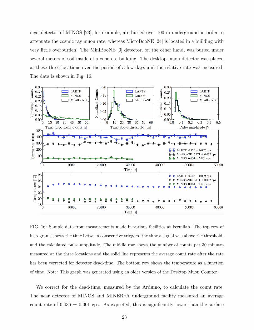
near detector of MINOS [23], for example, are buried over 100 m underground in order to
attenuate the cosmic ray muon rate, whereas MicroBooNE [24] is located in a building with
very little overburden. The MiniBooNE [3] detector, on the other hand, was buried under
several meters of soil inside of a concrete building. The desktop muon detector was placed
at these three locations over the period of a few days and the relative rate was measured.
The data is shown in Fig. 16.
FIG. 16: Sample data from measurements made in various facilities at Fermilab. The top row of
histograms shows the time between consecutive triggers, the time a signal was above the threshold,
and the calculated pulse amplitude. The middle row shows the number of counts per 30 minutes
measured at the three locations and the solid line represents the average count rate after the rate
has been corrected for detector dead-time. The bottom row shows the temperature as a function
of time. Note: This graph was generated using an older version of the Desktop Muon Counter.
We correct for the dead-time, measured by the Arduino, to calculate the count rate.
The near detector of MINOS and MINERνA underground facility measured an average
count rate of 0.036 ± 0.001 cps. As expected, this is significantly lower than the surface
23

experiments, MicroBooNE and MiniBooNE, whose rates were measured to be 0.236 ± 0.002
and 0.171 ± 0.002 cps, respectively. The lower rate at MiniBooNE was expected due to the
modest overburden.
The plastic scintillator was then removed from the counter and the background due to
dark noise triggers was measured. Over the course of 12 hours, there were zero counts in all
bins.
A Pearson’s Correlation Coefficient was then calculated to examine the correlation be-
tween count rate and temperature. With a 5 minute bin size, we find a correlation of
approximately 0.05, indicating a potentially weak correlation.
24
VIII. FINAL REMARKS
There are many interesting physics measurements that the device can be used to measure.
Variations of the project in the previous section could be:
1. Measure the relative depths of subway stations across the city, using the measured
muon rates.
2. Test relativistic time dilation on the cosmic ray flux by measuring the flux at various
elevations, such as in an airplane or on a mountain, compared to sea level[25].
3. Investigate seasonal variations in muon rates.
4. Using multiple detectors, measure the angular muon rate by looking at the coincidence
rate.
5. Lower the gain of the circuit to look at high-energy stopping muon events. Investigate
whether or not one can see the Michel electron from the muon decay.
The construction of desktop muon detectors will teach useful skills in the machine- and
electronics-shop. The code, libraries, and technical drawing are all provided. The time
scale for a student to produce a muon detector is expected to be less than 100 hours. Once
proficient with the machinery, we have found a student can produce more than one detector
per day. The total cost of a single detector is approximately $100 and may decrease in time
as SiPMs become less expensive.
Acknowledgments
This work is supported by the NSF grant 1505858. The authors would like to thank
those who taught Phys063 at Swarthmore College for the inspiration; J. Moon, D. Torretta,
and J. Zalesak for their aid in making the measurements at Fermilab; P. Sandstrom for
suggestions on the electronics design; and B. Jones for the idea of developing this idea for
25
the IceCube detector.
[1] Supplementary Material: S. Axani, Desktop-Muon-Detector, (2016), GitHub repository,
https://github.com/spenceraxani/Desktop-Muon-Detector
[2] Program: Physics and Astronomy, Swarthmore College, accessed: May 28, 2016, http://
catalog.swarthmore.edu/preview_program.php?catoid=7&poid=287#PHYS_063
[3] Aguilar-Arevalo, A. A., et al. “The miniboone detector.” Nuclear Instruments and Methods
in Physics Research Section A: Accelerators, Spectrometers, Detectors and Associated Equip-
ment 599.1 (2009): 28-46
[4] IceCube-PINGU Collaboration. “Letter of intent: The precision icecube next generation up-
grade (pingu).” arXiv preprint arXiv:1401.2046 (2014)
[5] Halzen, Francis, and Spencer R. Klein. “Invited review article: IceCube: an instrument for
neutrino astronomy.” Review of Scientific Instruments 81.8 (2010): 081101
[6] Saint-Gobain, Plastic Scintillation Products, accessed: May 28, 2016
[7] Eljen Technology, PLASTIC SCINTILLATORS, accessed: May 28, 2016
[8] RSS Specials, Elecrow Bazaar, accessed: May 28, 2016
[9] KiCad EDA, accessed Aug 6, 2016, http://kicad-pcb.org/
[10] Amazon, accessed Aug 6, 2016, http://www.Amazon.com
[11] DigiKey, accessed Aug 6, 2016, http://www.digikey.com/en
[12] Texas Instruments, accessed: May 28, 2016, http://www.ti.com/lit/ds/symlink/tlc080a.
[13] Horowitz, Paul, Winfield Hill, and Ian Robinson. The art of electronics. Vol. 1989. Cambridge:
Cambridge university press, 1980.
[14] C.F. Powell, Nobel Lecture, 1950, http://www.nobelprize.org/nobel_prizes/physics/
laureates/1950/powell-lecture.html
[15] Rossi, Bruno. “Interpretation of cosmic-ray phenomena.” Reviews of Modern Physics 20.3
(1948): 537
[16] B. Rossi, High Energy Particles (Prentice Hall, 1952)
[17] B. Rossi, Cosmic Rays (McGraw-Hill, 1964)
[18] The International Cosmic Ray Conference, http://icrc2015.nl/
26
[19] K.A. Olive et al. (Particle Data Group), Chin. Phys. C, 38, 090001 (2014) and 2015 update.
See, especially, Chapter 28 on Cosmic Rays. Online version: http://pdg.lbl.gov/, see Cosmic
Rays, listed under Reviews
[20] The Particle Adventure, accessed: May 28, 2016 http://www.particleadventure.org/
[21] Sanford Underground Research Facility, accessed: May 28, 2016 http://sanfordlab.org/
[22] Aliaga, L., et al. “Design, calibration, and performance of the MINERvA detector.” Nuclear
Instruments and Methods in Physics Research Section A: Accelerators, Spectrometers, Detec-
tors and Associated Equipment 743 (2014): 130-159
[23] Thomson, M. A. “Status of the MINOS Experiment.” Nuclear Physics B-Proceedings Supple-
ments 143 (2005): 249-256
[24] Jones, Benjamin JP. “The status of the MicroBooNE experiment.” Journal of Physics: Con-
ference Series. Vol. 408. No. 1. IOP Publishing, 2013
[25] Easwar, Nalini, and Douglas A. MacIntire. ”Study of the effect of relativistic time dilation
on cosmic ray muon fluxAn undergraduate modern physics experiment.” Am. J. Phys 59.7
(1991): 589-592
27