Embed Size (px)
Citation preview

Physics 123: Final Exam Spring 2013 1
Physics 123: Final Exam: Laboratory Electronics. Spring 2013
YOUR NAME: ___________________________
This is a mostly-closed-book test. You may use the following materials:
1. a one-page, one-sided handwritten ’cheat sheet’
2. a schematic diagram of the ’big board’ lab computer;
3. the thick xeroxed handout labeled “. . . References for Microcontroller,” detailing the 8051 instruction
set;
4. a calculator.
Also, please notice that these exam papers include some information that may be useful:
• An appendix at the end of the papers show some odds and ends:
– Some sketchy device data sheets:
∗ 3 op amps: ’411, ’358 & LMC6482 (rail-to-rail)
∗ 3 Comparators
∗ LM317/337 adjustable voltage regulator
∗ power MOSFET
∗ 555 oscillator
∗ analog switch (DG403)
∗ 74HC393 dual 4-bit ripple counter
∗ 74HC16xx 4-bit synchronous counters, natural binary and BCD
∗ 8051 port specifications
– a two-sheet reminder of some details of 8051 assembly language
Please remember to show your work, so that we can give partial credit for imperfect answers.
Total time : 180 minutes. Total points: 158 (analog: 62; digital: 96)
Physics 123: Final Exam Spring 2013 2
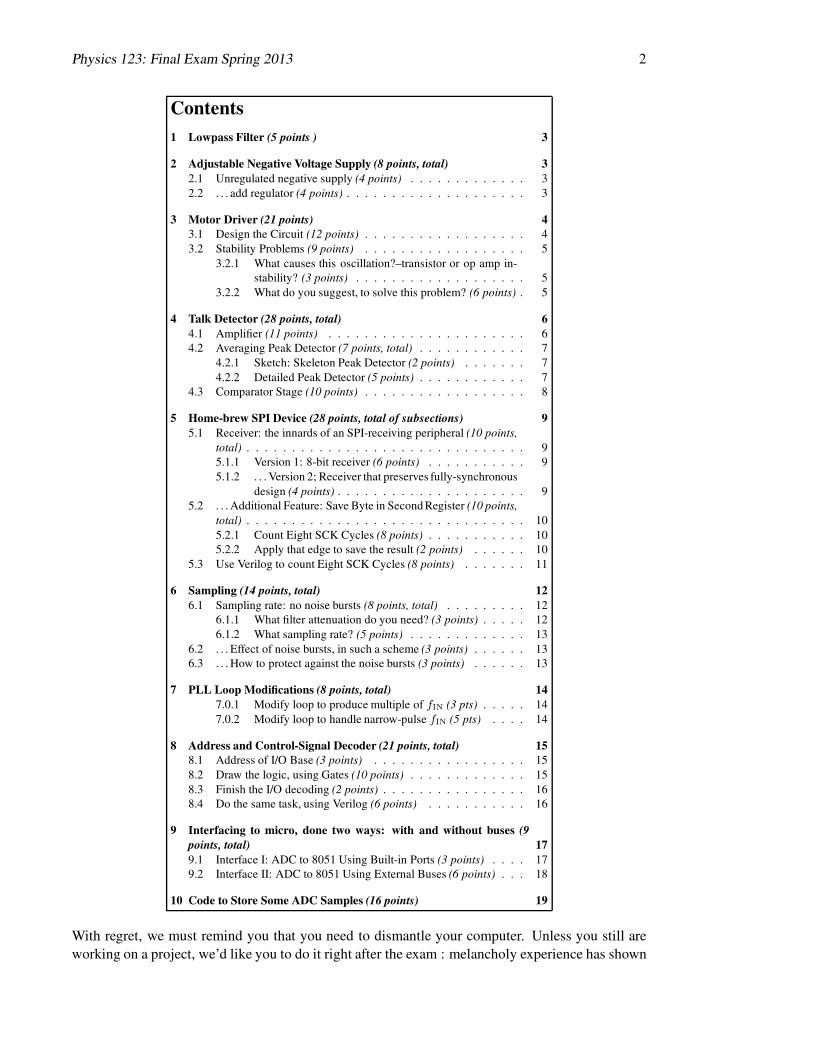
Contents
1 Lowpass Filter (5 points ) 3
2 Adjustable Negative Voltage Supply (8 points, total) 3
2.1 Unregulated negative supply (4 points) . . . . . . . . . . . . . 3
2.2 . . . add regulator (4 points) . . . . . . . . . . . . . . . . . . . . 3
3 Motor Driver (21 points) 4
3.1 Design the Circuit (12 points) . . . . . . . . . . . . . . . . . . 4
3.2 Stability Problems (9 points) . . . . . . . . . . . . . . . . . . 5
3.2.1 What causes this oscillation?–transistor or op amp in-
stability? (3 points) . . . . . . . . . . . . . . . . . . . 5
3.2.2 What do you suggest, to solve this problem? (6 points) . 5
4 Talk Detector (28 points, total) 6
4.1 Amplifier (11 points) . . . . . . . . . . . . . . . . . . . . . . 6
4.2 Averaging Peak Detector (7 points, total) . . . . . . . . . . . . 7
4.2.1 Sketch: Skeleton Peak Detector (2 points) . . . . . . . 7
4.2.2 Detailed Peak Detector (5 points) . . . . . . . . . . . . 7
4.3 Comparator Stage (10 points) . . . . . . . . . . . . . . . . . . 8
5 Home-brew SPI Device (28 points, total of subsections) 9
5.1 Receiver: the innards of an SPI-receiving peripheral (10 points,
total) . . . . . . . . . . . . . . . . . . . . . . . . . . . . . . . 9
5.1.1 Version 1: 8-bit receiver (6 points) . . . . . . . . . . . 9
5.1.2 . . . Version 2; Receiver that preserves fully-synchronous
design (4 points) . . . . . . . . . . . . . . . . . . . . . 9
5.2 . . . Additional Feature: Save Byte in Second Register (10 points,
total) . . . . . . . . . . . . . . . . . . . . . . . . . . . . . . . 10
5.2.1 Count Eight SCK Cycles (8 points) . . . . . . . . . . . 10
5.2.2 Apply that edge to save the result (2 points) . . . . . . 10
5.3 Use Verilog to count Eight SCK Cycles (8 points) . . . . . . . 11
6 Sampling (14 points, total) 12
6.1 Sampling rate: no noise bursts (8 points, total) . . . . . . . . . 12
6.1.1 What filter attenuation do you need? (3 points) . . . . . 12
6.1.2 What sampling rate? (5 points) . . . . . . . . . . . . . 13
6.2 . . . Effect of noise bursts, in such a scheme (3 points) . . . . . . 13
6.3 . . . How to protect against the noise bursts (3 points) . . . . . . 13
7 PLL Loop Modifications (8 points, total) 14
7.0.1 Modify loop to produce multiple of fIN (3 pts) . . . . . 14
7.0.2 Modify loop to handle narrow-pulse fIN (5 pts) . . . . 14
8 Address and Control-Signal Decoder (21 points, total) 15
8.1 Address of I/O Base (3 points) . . . . . . . . . . . . . . . . . 15
8.2 Draw the logic, using Gates (10 points) . . . . . . . . . . . . . 15
8.3 Finish the I/O decoding (2 points) . . . . . . . . . . . . . . . . 16
8.4 Do the same task, using Verilog (6 points) . . . . . . . . . . . 16
9 Interfacing to micro, done two ways: with and without buses (9
points, total) 17
9.1 Interface I: ADC to 8051 Using Built-in Ports (3 points) . . . . 17
9.2 Interface II: ADC to 8051 Using External Buses (6 points) . . . 18
10 Code to Store Some ADC Samples (16 points) 19
With regret, we must remind you that you need to dismantle your computer. Unless you still are
working on a project, we’d like you to do it right after the exam : melancholy experience has shown

Physics 123: Final Exam Spring 2013 3
us that people rarely return to take apart a computer, despite their good intentions. It’ll take you
only about 10 minutes.
ANALOG
1 Lowpass Filter (5 points )
Suppose you expect noise at frequencies 100kHz and up, and want to minimize it in an audio signal
that includes frequencies from about 20Hz to 20kHz. (The 100kHz is inaudible, of course; but it
can cause audible mischief in an audio amplifier.) Design this filter. Assume that you can tolerate
about 10% attenuation of signal, and that Rload ≥ 100kΩ.
2 Adjustable Negative Voltage Supply (8 points, total)
2.1 Unregulated negative supply (4 points)
Show a skeleton circuit (no part values needed) for a full-wave unregulated negative power supply.
Start with the 120V AC line voltage. Show switch, fuse, transformer, rectifier, filter capacitor (with
polarity shown), and attach output to a box labelled “regulator.”
2.2 . . . add regulator (4 points)Assume that your unregulated supply provides a negative 20V with 1 to 2V of ripple. Use an LM337
regulator to provide a regulated negative output voltage, adjustable in the range −5 to −15V. You’ll
find a sketchy ’337 data sheet at the end of these papers.
Physics 123: Final Exam Spring 2013 4
3 Motor Driver (21 points)
Here’s a problem that occurred recently, when we set about to re-use an old printer mechanism to
make a ruler-balancing machine (the old inverted-pendulum problem). The idea is to move the base
that supports the ruler so as to keep the ruler from falling over. (These details don’t matter at all to
your design, but you might possibly be interested to hear of a practical use for this circuit.)
The motor is to be controlled by the computer, through a DAC. The DAC is like the one used on
your computer, and its output voltage ranges from 0 to 2.55V. The motor needs a larger voltage,
symmetric about ground, and draws a lot of current: up to 1A. Your job is to design the driver
that can link the DAC to the motor. Note that this circuit should work down to DC (and very low
frequencies).
We’ll restate the specifications, here:
Supplies, etc. • power supply: ± 15V
• op amp output current limit: 25mA
• beta of power transistor: ≥ 50
DAC OUTPUT:
• voltage: 0 to 2.50V (8-bit converter: approximately 10mV/LSB) (Note that this output swing is not symmetric about
ground.)
• current: sink or source up to 1 mA
• output impedance: ≤ 100Ω
MOTOR:
• voltage range: -10V to +10V (these are the voltages your circuit should deliver to the motor, at the extremes of the DAC
range, 0V to 2.50V, respectively (0V should drive motor to -10V; 2.5V should drive motor to +10V).
• current: the motor will draw (sink or source) up to ±1A (at the extreme drive voltages)
3.1 Design the Circuit (12 points)
Physics 123: Final Exam Spring 2013 5
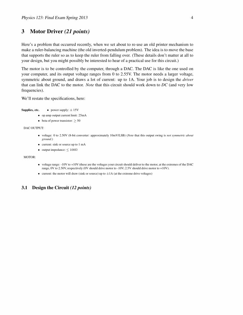
3.2 Stability Problems (9 points)
When we built this driver (using a ’411 op amp), attached a motor as load, and input a low-frequency
sine wave, here’s what input and output looked like:
Figure 1: motor noise, first view
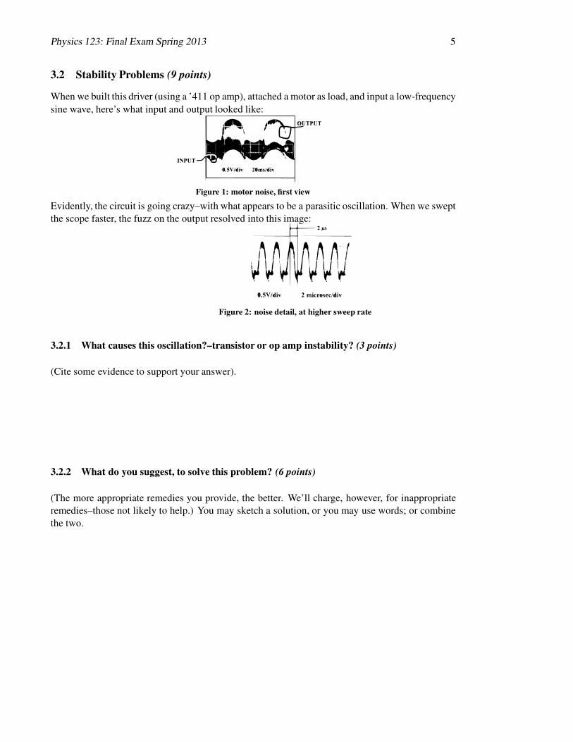
Evidently, the circuit is going crazy–with what appears to be a parasitic oscillation. When we swept
the scope faster, the fuzz on the output resolved into this image:
Figure 2: noise detail, at higher sweep rate
3.2.1 What causes this oscillation?–transistor or op amp instability? (3 points)
(Cite some evidence to support your answer).
3.2.2 What do you suggest, to solve this problem? (6 points)
(The more appropriate remedies you provide, the better. We’ll charge, however, for inappropriate
remedies–those not likely to help.) You may sketch a solution, or you may use words; or combine
the two.
Physics 123: Final Exam Spring 2013 6
4 Talk Detector (28 points, total)
The talker-machine with which Tom attempted a dialog recently is meant to respond when spoken to.
To do that trick (simulating intelligence; this is fake intelligence, to be distinguished from artificial
intelligence). It needs a circuit to determine when someone is speaking to it (or, more precisely, to
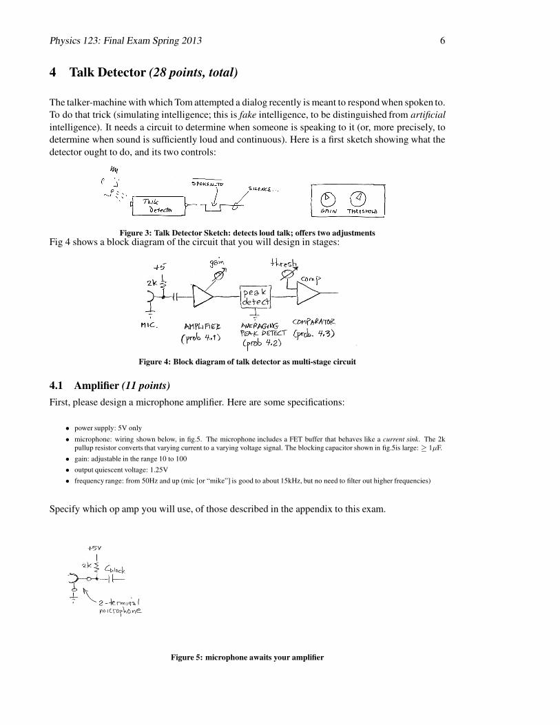
determine when sound is sufficiently loud and continuous). Here is a first sketch showing what the
detector ought to do, and its two controls:
Figure 3: Talk Detector Sketch: detects loud talk; offers two adjustments
Fig 4 shows a block diagram of the circuit that you will design in stages:
Figure 4: Block diagram of talk detector as multi-stage circuit
4.1 Amplifier (11 points)
First, please design a microphone amplifier. Here are some specifications:
• power supply: 5V only
• microphone: wiring shown below, in fig.5. The microphone includes a FET buffer that behaves like a current sink. The 2k
pullup resistor converts that varying current to a varying voltage signal. The blocking capacitor shown in fig.5is large: ≥ 1µF.
• gain: adjustable in the range 10 to 100
• output quiescent voltage: 1.25V
• frequency range: from 50Hz and up (mic [or “mike”] is good to about 15kHz, but no need to filter out higher frequencies)
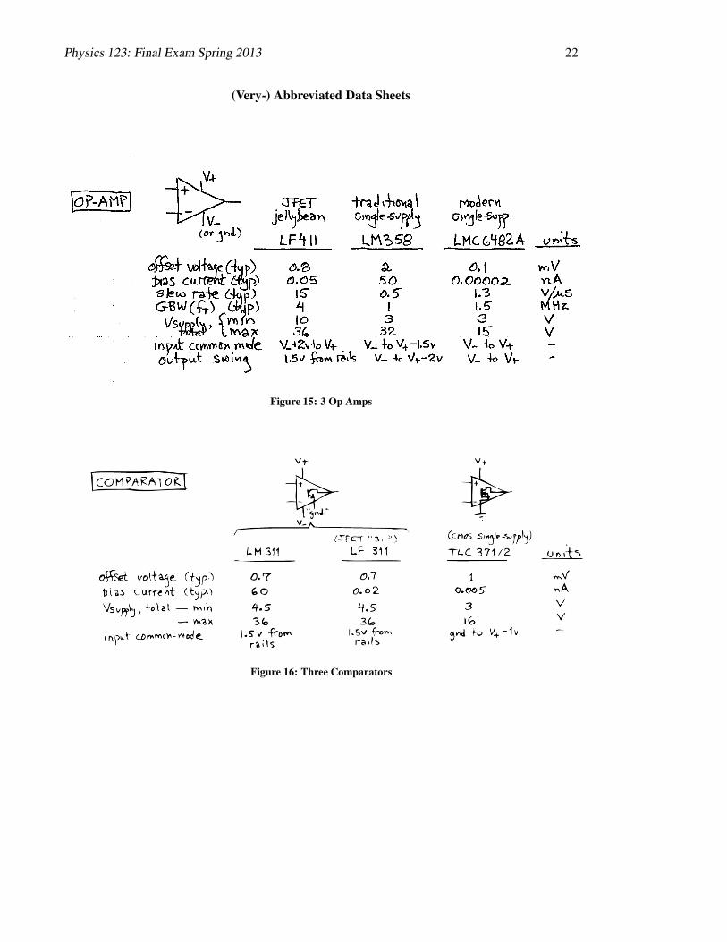
Specify which op amp you will use, of those described in the appendix to this exam.
Figure 5: microphone awaits your amplifier
Physics 123: Final Exam Spring 2013 7
4.2 Averaging Peak Detector (7 points, total)
In order to determine that someone is speaking to it loudly and persistently, the machine needs to
output a voltage whose level changes are roughly proportional to changes in the amplitude fed it
from the microphone. We’ll ask you to do this design in 2 stages: a sketch, then details.
4.2.1 Sketch: Skeleton Peak Detector (2 points)
First, please sketch a peak detector, without showing component values. This detector should put
out a voltage whose level varies with the average amplitude of the input signal. Output amplitude
need not equal the peak value of the input voltage. To say the same thing in other terms, the output
of this circuit should roughly follow the “envelope” of the input signal. When the input signal
amplitude shrinks, the detector output should gradually fall.
4.2.2 Detailed Peak Detector (5 points)
Now that you’ve shown the general scheme, let’s add details, this time including component values.
Here are the specifications:
• after talk ceases, the detector output should decline to its “silence” level in about 4 seconds
(roughly: 4 seconds ± perhaps 50%)
• the detector ought to pretty-much ignore transient noise, such as a short cough; the output
should move substantially only after an input signal has been present for about one second
Physics 123: Final Exam Spring 2013 8
4.3 Comparator Stage (10 points)
The output of your peak-detector stage will rise and fall gradually, with the loudness of speech at
the microphone. Now we need to add a comparator stage that will switch decisively in response to
the gradual changes of peak-detector levels. Here are some specifications for this stage:
• power supply: 5V only
• comparator output should go low when loud talk is detected
• switching threshold voltage should be adjustable, in a range from close to 1V to close to 3V
• hysteresis: about 0.2V
Specify which comparator you will use, of those described in the appendix to this exam.
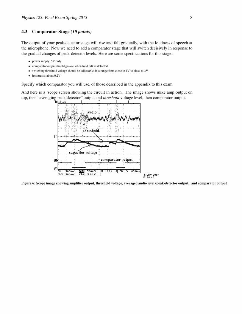
And here is a ’scope screen showing the circuit in action. The image shows mike amp output on
top, then “averaging peak detector” output and threshold voltage level, then comparator output.
Figure 6: Scope image showing amplifier output, threshold voltage, averaged audio level (peak-detector output), and comparator output
Physics 123: Final Exam Spring 2013 9
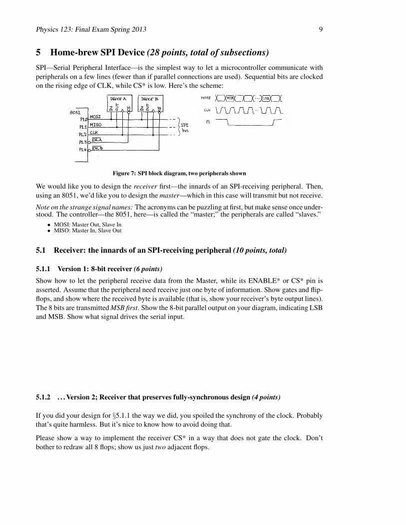
5 Home-brew SPI Device (28 points, total of subsections)
SPI—Serial Peripheral Interface—is the simplest way to let a microcontroller communicate with
peripherals on a few lines (fewer than if parallel connections are used). Sequential bits are clocked
on the rising edge of CLK, while CS* is low. Here’s the scheme:
Figure 7: SPI block diagram, two peripherals shown
We would like you to design the receiver first—the innards of an SPI-receiving peripheral. Then,
using an 8051, we’d like you to design the master—which in this case will transmit but not receive.
Note on the strange signal names: The acronyms can be puzzling at first, but make sense once under-stood. The controller—the 8051, here—is called the “master;” the peripherals are called “slaves.”
• MOSI: Master Out, Slave In• MISO: Master In, Slave Out
5.1 Receiver: the innards of an SPI-receiving peripheral (10 points, total)
5.1.1 Version 1: 8-bit receiver (6 points)
Show how to let the peripheral receive data from the Master, while its ENABLE* or CS* pin is
asserted. Assume that the peripheral need receive just one byte of information. Show gates and flip-
flops, and show where the received byte is available (that is, show your receiver’s byte output lines).
The 8 bits are transmitted MSB first. Show the 8-bit parallel output on your diagram, indicating LSB
and MSB. Show what signal drives the serial input.
5.1.2 . . . Version 2; Receiver that preserves fully-synchronous design (4 points)
If you did your design for §5.1.1 the way we did, you spoiled the synchrony of the clock. Probably
that’s quite harmless. But it’s nice to know how to avoid doing that.
Please show a way to implement the receiver CS* in a way that does not gate the clock. Don’t
bother to redraw all 8 flops; show us just two adjacent flops.
Physics 123: Final Exam Spring 2013 10
5.2 . . . Additional Feature: Save Byte in Second Register (10 points, total)
Once the 8 serial bits have arrived, they should be saved. Show how to implement this arrangement.
We will ask you to develop this circuitry in stages.
This additional circuitry should work as follows:
• count the SCK’s that occur after the assertion of the receiver’s CS*. Assume that CS* comes
at least 100ns before a clock edge.
• . . . when 8 rising edges have occurred, save the byte received by the Receiver of §§ 5.1.1 on
the previous page. . . , using the falling edge of SCK
Rather than start right in to draw your solution, please do this in two stages:
5.2.1 Count Eight SCK Cycles (8 points)
We need a rising edge to save the 8-bit value brought in by Receiver of §§ 5.1.1 on the preceding
page. This rising edge will save the byte in a byte-wide register.
Show how to generate a rising edge when 8 SCK’s have come in following assertion of CS*. Let
this rising-edge output be timed by the falling edge of SCK. The disassertion of CS* should clear
this counter, to make it ready for the next input cycle.1
You may design your circuit using D flip-flops plus gates, or use one of the five counters described
in an appendix to these exam notes: 74HC393 dual 4-bit ripple counter, or 74HC160..163 4-bit
synchronous counters. If you use one of the integrated devices, specify which counter you are
using.
5.2.2 Apply that edge to save the result (2 points)
Show how you would use that rising edge to save the receiver’s input byte. You may draw this add
your earlier drawing, in § 5.1.1 on the previous page, or you can give us a new sketch here.
1We assume that we are to receive one byte per assertion of CS*. This is not always the case.
Physics 123: Final Exam Spring 2013 11
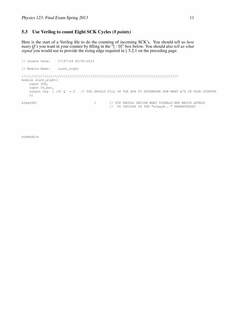
5.3 Use Verilog to count Eight SCK Cycles (8 points)
Here is the start of a Verilog file to do the counting of incoming SCK’s. You should tell us howmany Q’s you want in your counter by filling in the “[ : 0]” box below. You should also tell us whatsignal you would use to provide the rising edge required in § 5.2.1 on the preceding page.
// Create Date: 17:57:04 05/05/2013
// Module Name: count_eight
//////////////////////////////////////////////////////////////////////////////////
module count_eight(
input SCK,
input CS_bar,
output reg [ :0] Q = 0 // YOU SHOULD FILL IN THE BOX TO DETERMINE HOW MANY Q’S IN YOUR COUNTER
);
always@( ) // YOU SHOULD DECIDE WHAT SIGNALS AND WHICH LEVELS
// TO INCLUDE IN THE "alway@..." PARENTHESES
endmodule
Physics 123: Final Exam Spring 2013 12
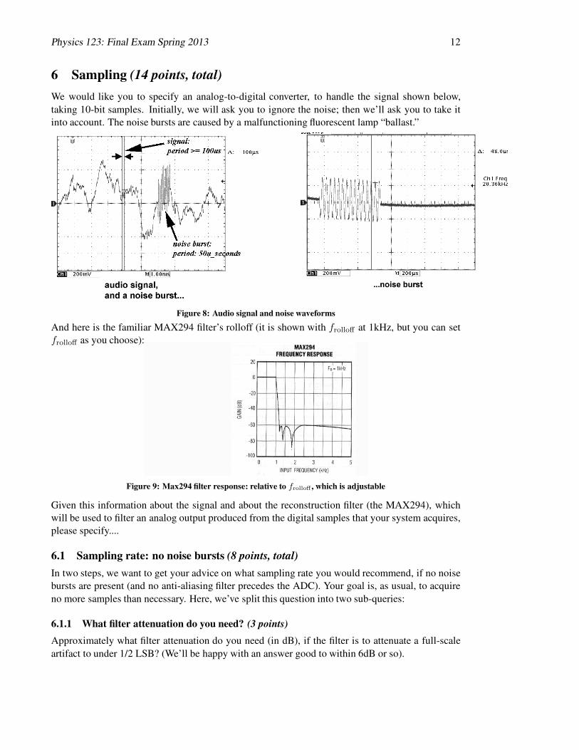
6 Sampling (14 points, total)
We would like you to specify an analog-to-digital converter, to handle the signal shown below,
taking 10-bit samples. Initially, we will ask you to ignore the noise; then we’ll ask you to take it
into account. The noise bursts are caused by a malfunctioning fluorescent lamp “ballast.”
Figure 8: Audio signal and noise waveforms
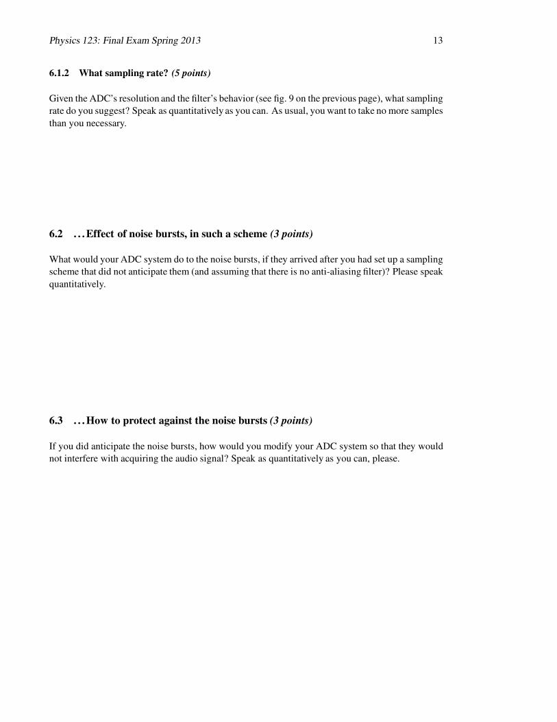
And here is the familiar MAX294 filter’s rolloff (it is shown with frolloff at 1kHz, but you can set
frolloff as you choose):
Figure 9: Max294 filter response: relative to frolloff , which is adjustable
Given this information about the signal and about the reconstruction filter (the MAX294), which
will be used to filter an analog output produced from the digital samples that your system acquires,
please specify....
6.1 Sampling rate: no noise bursts (8 points, total)
In two steps, we want to get your advice on what sampling rate you would recommend, if no noise
bursts are present (and no anti-aliasing filter precedes the ADC). Your goal is, as usual, to acquire
no more samples than necessary. Here, we’ve split this question into two sub-queries:
6.1.1 What filter attenuation do you need? (3 points)
Approximately what filter attenuation do you need (in dB), if the filter is to attenuate a full-scale
artifact to under 1/2 LSB? (We’ll be happy with an answer good to within 6dB or so).
Physics 123: Final Exam Spring 2013 13
6.1.2 What sampling rate? (5 points)
Given the ADC’s resolution and the filter’s behavior (see fig. 9 on the previous page), what sampling
rate do you suggest? Speak as quantitatively as you can. As usual, you want to take no more samples
than you necessary.
6.2 . . . Effect of noise bursts, in such a scheme (3 points)
What would your ADC system do to the noise bursts, if they arrived after you had set up a sampling
scheme that did not anticipate them (and assuming that there is no anti-aliasing filter)? Please speak
quantitatively.
6.3 . . . How to protect against the noise bursts (3 points)
If you did anticipate the noise bursts, how would you modify your ADC system so that they would
not interfere with acquiring the audio signal? Speak as quantitatively as you can, please.
Physics 123: Final Exam Spring 2013 14
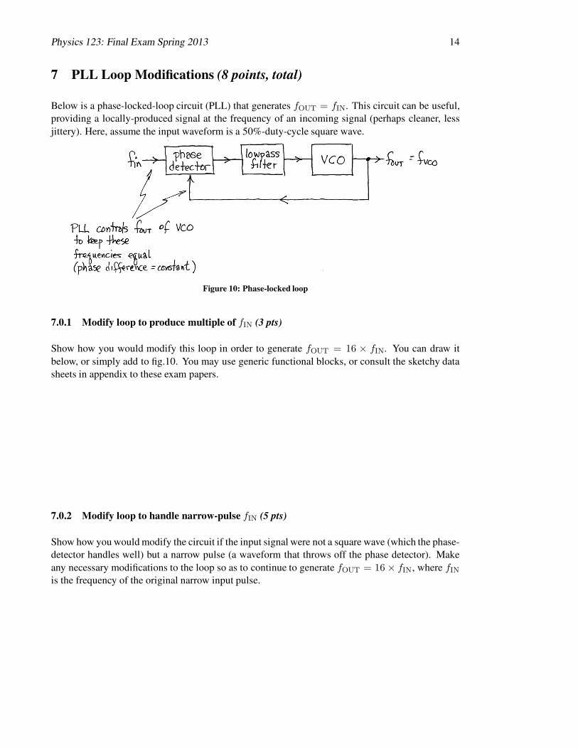
7 PLL Loop Modifications (8 points, total)
Below is a phase-locked-loop circuit (PLL) that generates fOUT = fIN. This circuit can be useful,
providing a locally-produced signal at the frequency of an incoming signal (perhaps cleaner, less
jittery). Here, assume the input waveform is a 50%-duty-cycle square wave.
Figure 10: Phase-locked loop
7.0.1 Modify loop to produce multiple of fIN (3 pts)
Show how you would modify this loop in order to generate fOUT = 16 × fIN. You can draw it
below, or simply add to fig.10. You may use generic functional blocks, or consult the sketchy data
sheets in appendix to these exam papers.
7.0.2 Modify loop to handle narrow-pulse fIN (5 pts)
Show how you would modify the circuit if the input signal were not a square wave (which the phase-
detector handles well) but a narrow pulse (a waveform that throws off the phase detector). Make
any necessary modifications to the loop so as to continue to generate fOUT = 16 × fIN, where fIN
is the frequency of the original narrow input pulse.
Physics 123: Final Exam Spring 2013 15
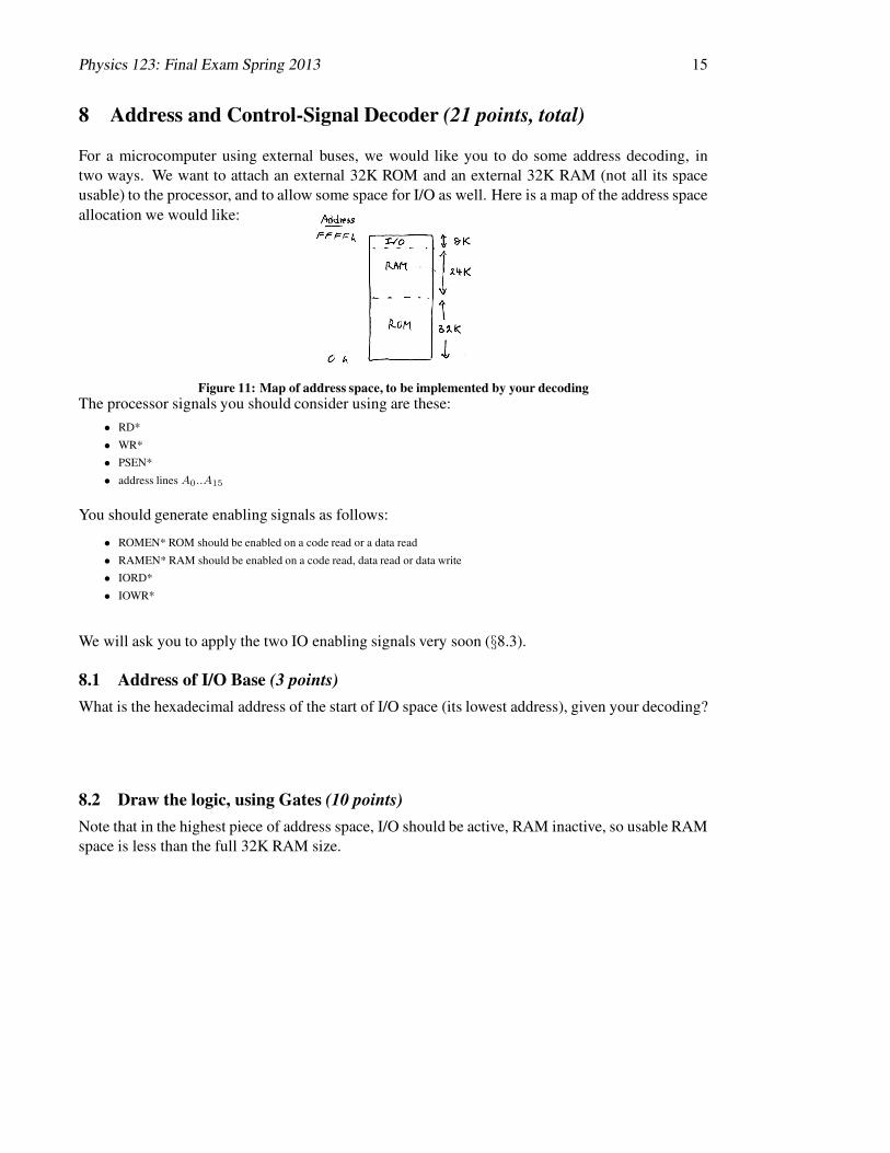
8 Address and Control-Signal Decoder (21 points, total)
For a microcomputer using external buses, we would like you to do some address decoding, in
two ways. We want to attach an external 32K ROM and an external 32K RAM (not all its space
usable) to the processor, and to allow some space for I/O as well. Here is a map of the address space
allocation we would like:
Figure 11: Map of address space, to be implemented by your decoding
The processor signals you should consider using are these:
• RD*
• WR*
• PSEN*
• address lines A0..A15
You should generate enabling signals as follows:
• ROMEN* ROM should be enabled on a code read or a data read
• RAMEN* RAM should be enabled on a code read, data read or data write
• IORD*
• IOWR*
We will ask you to apply the two IO enabling signals very soon (§8.3).
8.1 Address of I/O Base (3 points)
What is the hexadecimal address of the start of I/O space (its lowest address), given your decoding?
8.2 Draw the logic, using Gates (10 points)
Note that in the highest piece of address space, I/O should be active, RAM inactive, so usable RAM
space is less than the full 32K RAM size.
Physics 123: Final Exam Spring 2013 16
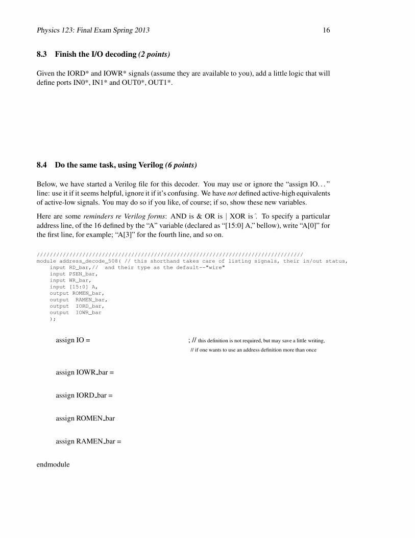
8.3 Finish the I/O decoding (2 points)
Given the IORD* and IOWR* signals (assume they are available to you), add a little logic that will
define ports IN0*, IN1* and OUT0*, OUT1*.
8.4 Do the same task, using Verilog (6 points)
Below, we have started a Verilog file for this decoder. You may use or ignore the “assign IO. . . ”
line: use it if it seems helpful, ignore it if it’s confusing. We have not defined active-high equivalents
of active-low signals. You may do so if you like, of course; if so, show these new variables.
Here are some reminders re Verilog forms: AND is & OR is | XOR is . To specify a particular
address line, of the 16 defined by the “A” variable (declared as “[15:0] A,” bellow), write “A[0]” for
the first line, for example; “A[3]” for the fourth line, and so on.
//////////////////////////////////////////////////////////////////////////////////
module address_decode_508( // this shorthand takes care of listing signals, their in/out status,
input RD_bar,// and their type as the default--"wire"
input PSEN_bar,
input WR_bar,
input [15:0] A,
output ROMEN_bar,
output RAMEN_bar,
output IORD_bar,
output IOWR_bar
);
assign IO = ; // this definition is not required, but may save a little writing,
// if one wants to use an address definition more than once
assign IOWR bar =
assign IORD bar =
assign ROMEN bar
assign RAMEN bar =
endmodule
Physics 123: Final Exam Spring 2013 17
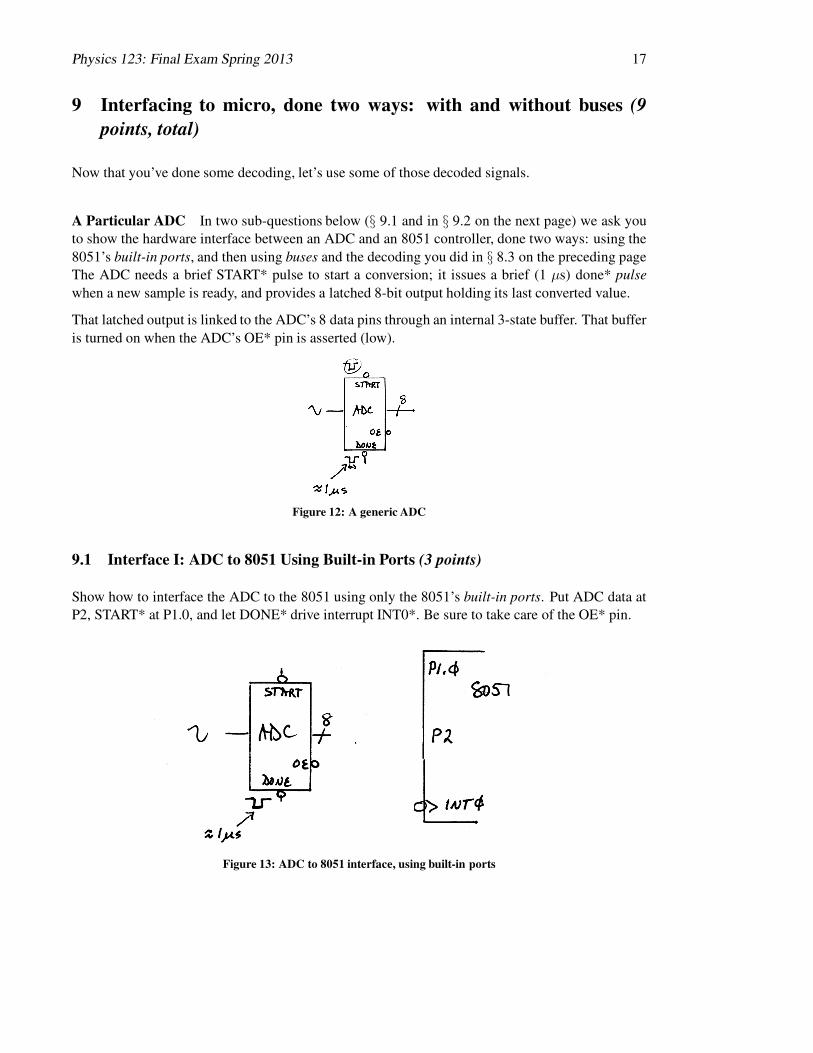
9 Interfacing to micro, done two ways: with and without buses (9
points, total)
Now that you’ve done some decoding, let’s use some of those decoded signals.
A Particular ADC In two sub-questions below (§ 9.1 and in § 9.2 on the next page) we ask you
to show the hardware interface between an ADC and an 8051 controller, done two ways: using the
8051’s built-in ports, and then using buses and the decoding you did in § 8.3 on the preceding page
The ADC needs a brief START* pulse to start a conversion; it issues a brief (1 µs) done* pulse
when a new sample is ready, and provides a latched 8-bit output holding its last converted value.
That latched output is linked to the ADC’s 8 data pins through an internal 3-state buffer. That buffer
is turned on when the ADC’s OE* pin is asserted (low).
Figure 12: A generic ADC
9.1 Interface I: ADC to 8051 Using Built-in Ports (3 points)
Show how to interface the ADC to the 8051 using only the 8051’s built-in ports. Put ADC data at
P2, START* at P1.0, and let DONE* drive interrupt INT0*. Be sure to take care of the OE* pin.
Figure 13: ADC to 8051 interface, using built-in ports
Physics 123: Final Exam Spring 2013 18
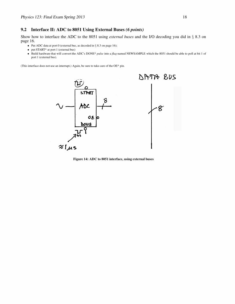
9.2 Interface II: ADC to 8051 Using External Buses (6 points)
Show how to interface the ADC to the 8051 using external buses and the I/O decoding you did in § 8.3 onpage 16.
• Put ADC data at port 0 (external bus, as decoded in § 8.3 on page 16);
• put START* at port 1 (external bus)
• Build hardware that will convert the ADC’s DONE* pulse into a flag named NEWSAMPLE which the 8051 should be able to poll at bit 1 of
port 1 (external bus).
(This interface does not use an interrupt.) Again, be sure to take care of the OE* pin.
Figure 14: ADC to 8051 interface, using external buses
Physics 123: Final Exam Spring 2013 19
10 Code to Store Some ADC Samples (16 points)
We’d like you to write some code assuming the simpler hardware of § 9.1 on page 17: there, the
interface is done with the 8051’s built-in ports.
Here’s what we’d like the code to do:
• get a sample using the following procedure:
– start the ADC with a START* pulse;
– when the DONE* signal interrupts the 8051 (edge-sensitive) your ISR should set a soft-
ware flag named SAMPLED BIT; this flag lives in a bit-addressable on-chip location (it
happens to live at bit zero, as defined below, but that doesn’t matter to your code).
– . . . When the main program finds that the flag SAMPLED BIT is asserted, it reads one
ADC sample. . .
• . . . and stores it in the external RAM table. This table is in (external-) RAM beginning at the
first RAM location defined by your decoding of § 8.3 on page 16. (This is RAM that often is
described as “MOVX RAM.” It was on-chip for the SiLabs part, off-chip for the Dallas part).
• when 128 samples have been stored, let the program stop (it can do this by using a line that
jumps to itself).
On the next page we have written a framework for your code. We have tried to take care of boring
details. We have written a routine, for example, that initializes interrupts.
But you need to decide where to invoke that routine—named “INTENABLE.” Your code should
call the routine.
Physics 123: Final Exam Spring 2013 20
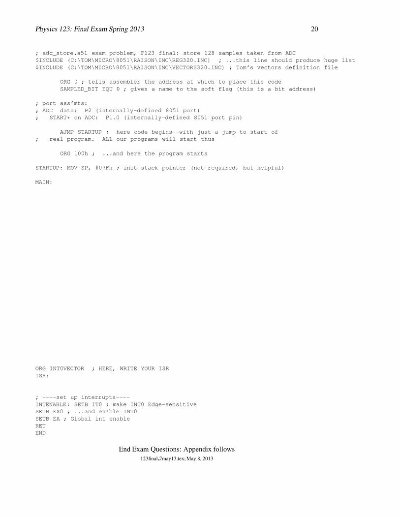
; adc_store.a51 exam problem, P123 final: store 128 samples taken from ADC
$INCLUDE (C:\TOM\MICRO\8051\RAISON\INC\REG320.INC) ; ...this line should produce huge list
$INCLUDE (C:\TOM\MICRO\8051\RAISON\INC\VECTORS320.INC) ; Tom’s vectors definition file
ORG 0 ; tells assembler the address at which to place this code
SAMPLED_BIT EQU 0 ; gives a name to the soft flag (this is a bit address)
; port ass’mts:
; ADC data: P2 (internally-defined 8051 port)
; START* on ADC: P1.0 (internally-defined 8051 port pin)
AJMP STARTUP ; here code begins--with just a jump to start of
; real program. ALL our programs will start thus
ORG 100h ; ...and here the program starts
STARTUP: MOV SP, #07Fh ; init stack pointer (not required, but helpful)
MAIN:
ORG INT0VECTOR ; HERE, WRITE YOUR ISR
ISR:
; ----set up interrupts----
INTENABLE: SETB IT0 ; make INT0 Edge-sensitive
SETB EX0 ; ...and enable INT0
SETB EA ; Global int enable
RET
END
End Exam Questions: Appendix follows
123final 7may13.tex; May 8, 2013
Physics 123: Final Exam Spring 2013 21
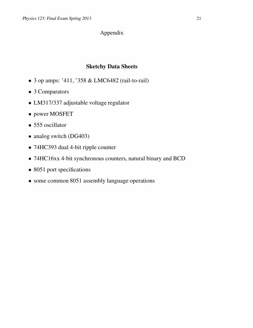
Appendix
Sketchy Data Sheets
• 3 op amps: ’411, ’358 & LMC6482 (rail-to-rail)
• 3 Comparators
• LM317/337 adjustable voltage regulator
• power MOSFET
• 555 oscillator
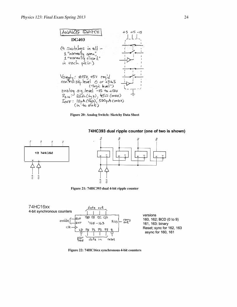
• analog switch (DG403)
• 74HC393 dual 4-bit ripple counter
• 74HC16xx 4-bit synchronous counters, natural binary and BCD
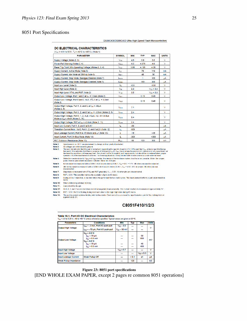
• 8051 port specifications
• some common 8051 assembly language operations
Physics 123: Final Exam Spring 2013 22
(Very-) Abbreviated Data Sheets
Figure 15: 3 Op Amps
Figure 16: Three Comparators
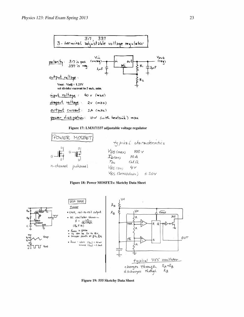
Physics 123: Final Exam Spring 2013 23
Figure 17: LM317/337 adjustable voltage regulator
Figure 18: Power MOSFETs: Sketchy Data Sheet
Figure 19: 555 Sketchy Data Sheet
Physics 123: Final Exam Spring 2013 24
Figure 20: Analog Switch: Sketchy Data Sheet
Figure 21: 74HC393 dual 4-bit ripple counter
Figure 22: 74HC16xx synchronous 4-bit counters
Physics 123: Final Exam Spring 2013 25
8051 Port Specifications
Figure 23: 8051 port specifications
[END WHOLE EXAM PAPER, except 2 pages re common 8051 operations]
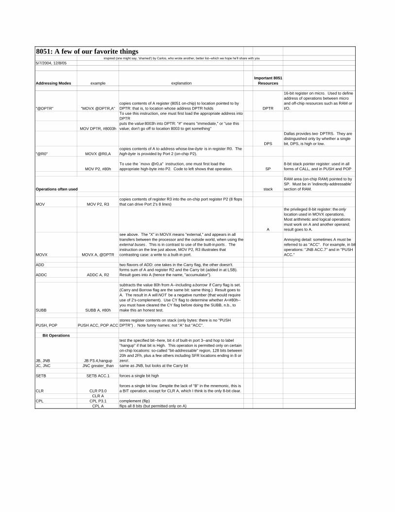
8051: A few of our favorite thingsinspired (one might say, 'shamed') by Carlos, who wrote another, better list--which we hope he'll share with you
5/7/2004, 12/8/05
Addressing Modes example explanationImportant 8051
Resources
"@DPTR" "MOVX @DPTR,A"copies contents of A register (8051 on-chip) to location pointed to by DPTR: that is, to location whose address DPTR holds DPTR
16-bit register on micro. Used to define address of operations between micro and off-chip resources such as RAM or I/O.
To use this instruction, one must first load the appropriate address into DPTR
MOV DPTR, #8003hputs the value 8003h into DPTR: "#" means "immediate," or "use this value; don't go off to location 8003 to get something"
DPS
Dallas provides two DPTRS. They are distinguished only by whether a single bit, DPS, is high or low.
"@R0" MOVX @R0,Acopies contents of A to address whose low-byte is in register R0. The high-byte is provided by Port 2 (on-chip P2).
MOV P2, #80hTo use the `movx @r0,a" instruction, one must first load the appropriate high-byte into P2. Code to left shows that operation. SP
8-bit stack pointer register: used in all forms of CALL, and in PUSH and POP
Operations often used stack
RAM area (on-chip RAM) pointed to by SP. Must be in 'indirectly-addressable' section of RAM.
MOV MOV P2, R3copies contents of register R3 into the on-chip port register P2 (8 flops that can drive Port 2's 8 lines)
A
the privileged 8-bit register: the only location used in MOVX operations. Most arithmetic and logical operations must work on A and another operand; result goes to A.
MOVX MOVX A, @DPTR
see above. The "X" in MOVX means "external," and appears in all transfers between the processor and the outside world, when using the external buses . This is in contrast to use of the built-in ports . The instruction on the line just above, MOV P2, R3 illustrates that contrasting case: a write to a built-in port.
Annoying detail: sometimes A must be referred to as "ACC". For example, in bitoperations: "JNB ACC.7" and in "PUSH ACC."
ADD two flavors of ADD: one takes in the Carry flag, the other doesn't.
ADDC ADDC A, R2forms sum of A and register R2 and the Carry bit (added in at LSB). Result goes into A (hence the name, "accumulator").
SUBB SUBB A, #80h
subtracts the value 80h from A--including a borrow if Carry flag is set. (Carry and Borrow flag are the same bit: same thing.) Result goes to A. The result in A will NOT be a negative number (that would require use of 2's-complement). Use CY flag to determine whether A<#80h--you must have cleared the CY flag before doing the SUBB, n.b., to make this an honest test.
PUSH, POP PUSH ACC, POP ACCstores register contents on stack (only bytes: there is no "PUSH DPTR") . Note funny names: not "A" but "ACC".
Bit Operations
JB, JNB JB P3.4,hangup
test the specified bit--here, bit 4 of built-in port 3--and hop to label "hangup" if that bit is High. This operation is permitted only on certain on-chip locations: so-called "bit-addressable" region, 128 bits between 20h and 2Fh, plus a few others including SFR locations ending in 8 or zero!.
JC, JNC JNC greater_than same as JNB, but looks at the Carry bit
SETB SETB ACC.1 forces a single bit high
CLR CLR P3.0forces a single bit low. Despite the lack of "B" in the mnemonic, this is a BIT operation, except for CLR A, which I think is the only 8-bit clear.
CLR ACPL CPL P3.1 complement (flip)
CPL A flips all 8 bits (but permitted only on A)
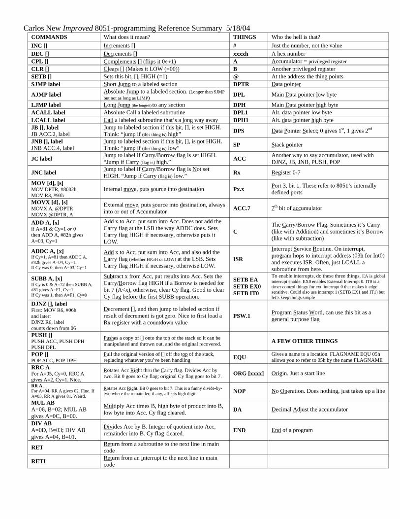
Carlos New Improved 8051-programming Reference Summary 5/18/04 COMMANDS What does it mean? THINGS Who the hell is that? INC [] Increments [] # Just the number, not the value DEC [] Decrements [] xxxxh A hex number CPL [] Complements [] (flips it 0↔1) A Accumulator = privileged register CLR [] Clears [] (Makes it LOW (=00)) B Another privileged register SETB [] Sets this bit, [], HIGH (=1) @ At the address the thing points SJMP label Short Jump to a labeled section DPTR Data pointer
AJMP label Absolute Jump to a labeled section. (Longer than SJMP but not as long as LJMP) DPL Main Data pointer low byte
LJMP label Long Jump (the longest) to any section DPH Main Data pointer high byte ACALL label Absolute Call a labeled subroutine DPL1 Alt. data pointer low byte LCALL label Call a labeled subroutine that’s a long way away DPH1 Alt. data pointer high byte JB [], label JB ACC.2, label
Jump to labeled section if this bit, [], is set HIGH. Think: “jump if (this thing is) high” DPS Data Pointer Select; 0 gives 1st, 1 gives 2nd
JNB [], label JNB ACC.4, label
Jump to labeled section if this bit, [], is not HIGH. Think: “jump if (this thing is) low” SP Stack pointer
JC label Jump to label if Carry/Borrow flag is set HIGH. “Jump if Carry (flag is) high.” ACC Another way to say accumulator, used with
DJNZ, JB, JNB, PUSH, POP
JNC label Jump to label if Carry/Borrow flag is Not set HIGH. “Jump if Carry (flag is) low.” Rx Register 0-7
MOV [d], [s] MOV DPTR, #8002h MOV R3, #93h
Internal move, puts source into destination Px.x Port 3, bit 1. These refer to 8051’s internally defined ports
MOVX [d], [s] MOVX A, @DPTR MOVX @DPTR, A
External move, puts source into destination, always into or out of Accumulator ACC.7 7th bit of accumulator
ADD A, [x] if A=81 & Cy=1 or 0 then ADD A, #82h gives A=03, Cy=1
Add x to Acc, put sum into Acc. Does not add the Carry flag at the LSB the way ADDC does. Sets Carry flag HIGH if necessary, otherwise puts it LOW.
C The Carry/Borrow Flag. Sometimes it’s Carry (like with Addition) and sometimes it’s Borrow (like with subtraction)
ADDC A, [x] If Cy=1, A=81 then ADDC A, #82h gives A=04, Cy=1. If Cy was 0, then A=03, Cy=1
Add x to Acc, put sum into Acc, and also add the Carry flag (whether HIGH or LOW) at the LSB. Sets Carry flag HIGH if necessary, otherwise LOW.
ISR
Interrupt Service Routine. On interrupt, program hops to interrupt address (03h for Int0) and executes ISR. Often, just LCALL a subroutine from here.
SUBB A, [x] If Cy is 0 & A=72 then SUBB A, #81 gives A=F1, Cy=1. If Cy was 1, then A=F1, Cy=0
Subtract x from Acc, put results into Acc. Sets the Carry/Borrow flag HIGH if a Borrow is needed for bit 7 (A<x), otherwise, clear Cy flag. Good to clear Cy flag before the first SUBB operation.
SETB EA SETB EX0 SETB IT0
To enable interrupts, do these three things. EA is global interrupt enable. EX0 enables External Interrupt 0. IT0 is a timer control thingy for ext. interrupt 0 that makes it edge sensitive. Could also use interrupt 1 (SETB EX1 and IT1) but let’s keep things simple
DJNZ [], label First: MOV R6, #06h and later: DJNZ R6, label counts down from 06
Decrement [], and then jump to labeled section if result of decrement is not zero. Nice to first load a Rx register with a countdown value
PSW.1 Program Status Word, can use this bit as a general purpose flag
PUSH [] PUSH ACC, PUSH DPH PUSH DPL
Pushes a copy of [] onto the top of the stack so it can be manipulated and thrown out, and the original recovered. A FEW OTHER THINGS
POP [] POP ACC, POP DPH
Pull the original version of [] off the top of the stack, replacing whatever you’ve been handling EQU Gives a name to a location. FLAGNAME EQU 05h
allows you to refer to 05h by the name FLAGNAME RRC A For A=05, Cy=0, RRC A gives A=2, Cy=1. Nice.
Rotates Acc Right thru the Carry flag. Divides Acc by two. Bit 0 goes to Cy flag; original Cy flag goes to bit 7. ORG [xxxx] Origin. Just a start line
RR A For A=04, RR A gives 02. Fine. If A=03, RR A gives 81. Weird.
Rotates Acc Right. Bit 0 goes to bit 7. This is a funny divide-by-two where the remainder, if any, affects high digit. NOP No Operation. Does nothing, just takes up a line
MUL AB A=06, B=02; MUL AB gives A=0C, B=00.
Multiply Acc times B, high byte of product into B, low byte into Acc. Cy flag cleared. DA Decimal Adjust the accumulator
DIV AB A=0D, B=03; DIV AB gives A=04, B=01.
Divides Acc by B. Integer of quotient into Acc, remainder into B. Cy flag cleared. END End of a program
RET Return from a subroutine to the next line in main code
RETI Return from an interrupt to the next line in main code