Embed Size (px)
Citation preview
ARTICLE IN PRESS
Physica E 41 (2009) 325–344
Contents lists available at ScienceDirect
Physica E
1386-94
doi:10.1
� Corr
E-m
journal homepage: www.elsevier.com/locate/physe
Review
Hybrid molecule-on-silicon nanoelectronics: Electrochemical processes forgrafting and printing of monolayers
D.K. Aswal a,b,�, S.P. Koiry b, B. Jousselme a, S.K. Gupta b, S. Palacin a, J.V. Yakhmi b
a CEA, IRAMIS, SPCSI, Chemistry of Surfaces and Interfaces, F-91191 Gif sur Yvette Cedex, Franceb Technical Physics and Prototype Engineering Division, Bhabha Atomic Research Centre, Trombay, Mumbai 400 085, India
a r t i c l e i n f o
Article history:
Received 3 September 2008
Received in revised form
16 November 2008
Accepted 17 November 2008Available online 24 November 2008
PACS:
81.15.Pq
81.16.Pr
81.07.Nb
85.65._h
Keywords:
Electrografting
Monolayers
Hybrid nanoelectronics
Electrochemical printing
77/$ - see front matter & 2008 Elsevier B.V. A
016/j.physe.2008.11.001
esponding author.
ail address: [email protected] (D.K. Aswal)
a b s t r a c t
The hybrid nanoelectronics, i.e., organic molecules deposited on Si exhibiting electronic functionalities
is expected to extend the scaling limits of Si microelectronics down to few nanometers. In this review,
first we make an overview of the organic molecules exhibiting various functionalities, such as,
dielectric, diode, memory and transistor. We then review the literature on electrochemical grafting of
organic molecules to Si, which have been carried out using terminal vinyl (CQC), ethynyl (CRC),
halide (Cl, Br, I), tetraalkylammonium salt, diazonium salt and silane as reactant. It has been
demonstrated that electrochemistry not only allows grafting of molecules on Si but also provides very
useful information on the characteristics of the grafted layers. The electronic functionalities of various
electrografted molecules are discussed. An additional advantage of the electrochemical process is that
monolayer patterns with spatial resolution in a wide range, i.e. from nanometer to millimeter, can
be easily prepared. The recent advances made in the spatial patterning of monolayers using
electrochemical lithography are briefly reviewed.
& 2008 Elsevier B.V. All rights reserved.
Contents
1. Introduction . . . . . . . . . . . . . . . . . . . . . . . . . . . . . . . . . . . . . . . . . . . . . . . . . . . . . . . . . . . . . . . . . . . . . . . . . . . . . . . . . . . . . . . . . . . . . . . . . . . . . . 326
2. Organic molecules exhibiting electronic functionalities. . . . . . . . . . . . . . . . . . . . . . . . . . . . . . . . . . . . . . . . . . . . . . . . . . . . . . . . . . . . . . . . . . . . 327
2.1. Molecular dielectrics and wires. . . . . . . . . . . . . . . . . . . . . . . . . . . . . . . . . . . . . . . . . . . . . . . . . . . . . . . . . . . . . . . . . . . . . . . . . . . . . . . . . 328
2.2. Molecular diodes . . . . . . . . . . . . . . . . . . . . . . . . . . . . . . . . . . . . . . . . . . . . . . . . . . . . . . . . . . . . . . . . . . . . . . . . . . . . . . . . . . . . . . . . . . . . 328
2.3. Molecular memories . . . . . . . . . . . . . . . . . . . . . . . . . . . . . . . . . . . . . . . . . . . . . . . . . . . . . . . . . . . . . . . . . . . . . . . . . . . . . . . . . . . . . . . . . 328
2.4. Molecular transistors . . . . . . . . . . . . . . . . . . . . . . . . . . . . . . . . . . . . . . . . . . . . . . . . . . . . . . . . . . . . . . . . . . . . . . . . . . . . . . . . . . . . . . . . . 329
3. Hydrogen-terminated silicon surfaces . . . . . . . . . . . . . . . . . . . . . . . . . . . . . . . . . . . . . . . . . . . . . . . . . . . . . . . . . . . . . . . . . . . . . . . . . . . . . . . . . 329
4. Electrochemical grafting of organic molecules . . . . . . . . . . . . . . . . . . . . . . . . . . . . . . . . . . . . . . . . . . . . . . . . . . . . . . . . . . . . . . . . . . . . . . . . . . . 329
4.1. Terminal vinyl (CQC) as reactant . . . . . . . . . . . . . . . . . . . . . . . . . . . . . . . . . . . . . . . . . . . . . . . . . . . . . . . . . . . . . . . . . . . . . . . . . . . . . . . 330
4.2. Terminal ethynyl (CRC) as reactant . . . . . . . . . . . . . . . . . . . . . . . . . . . . . . . . . . . . . . . . . . . . . . . . . . . . . . . . . . . . . . . . . . . . . . . . . . . . . 333
4.3. Terminal halide as reactant . . . . . . . . . . . . . . . . . . . . . . . . . . . . . . . . . . . . . . . . . . . . . . . . . . . . . . . . . . . . . . . . . . . . . . . . . . . . . . . . . . . . . 333
4.4. Tetraalkylammonium salts . . . . . . . . . . . . . . . . . . . . . . . . . . . . . . . . . . . . . . . . . . . . . . . . . . . . . . . . . . . . . . . . . . . . . . . . . . . . . . . . . . . . . 334
4.5. Diazonium and iodonium salts . . . . . . . . . . . . . . . . . . . . . . . . . . . . . . . . . . . . . . . . . . . . . . . . . . . . . . . . . . . . . . . . . . . . . . . . . . . . . . . . . . 334
4.6. Silanes . . . . . . . . . . . . . . . . . . . . . . . . . . . . . . . . . . . . . . . . . . . . . . . . . . . . . . . . . . . . . . . . . . . . . . . . . . . . . . . . . . . . . . . . . . . . . . . . . . . . . 336
5. Electrochemical printing of monolayers . . . . . . . . . . . . . . . . . . . . . . . . . . . . . . . . . . . . . . . . . . . . . . . . . . . . . . . . . . . . . . . . . . . . . . . . . . . . . . . . 339
5.1. Nanowriting . . . . . . . . . . . . . . . . . . . . . . . . . . . . . . . . . . . . . . . . . . . . . . . . . . . . . . . . . . . . . . . . . . . . . . . . . . . . . . . . . . . . . . . . . . . . . . . . . 339
5.2. Nanolithography . . . . . . . . . . . . . . . . . . . . . . . . . . . . . . . . . . . . . . . . . . . . . . . . . . . . . . . . . . . . . . . . . . . . . . . . . . . . . . . . . . . . . . . . . . . . . 340
5.3. Micropatterning . . . . . . . . . . . . . . . . . . . . . . . . . . . . . . . . . . . . . . . . . . . . . . . . . . . . . . . . . . . . . . . . . . . . . . . . . . . . . . . . . . . . . . . . . . . . . . 341
6. Summary . . . . . . . . . . . . . . . . . . . . . . . . . . . . . . . . . . . . . . . . . . . . . . . . . . . . . . . . . . . . . . . . . . . . . . . . . . . . . . . . . . . . . . . . . . . . . . . . . . . . . . . . 342
Acknowledgements . . . . . . . . . . . . . . . . . . . . . . . . . . . . . . . . . . . . . . . . . . . . . . . . . . . . . . . . . . . . . . . . . . . . . . . . . . . . . . . . . . . . . . . . . . . . . . . . 342
References . . . . . . . . . . . . . . . . . . . . . . . . . . . . . . . . . . . . . . . . . . . . . . . . . . . . . . . . . . . . . . . . . . . . . . . . . . . . . . . . . . . . . . . . . . . . . . . . . . . . . . . 342
ll rights reserved.
.
ARTICLE IN PRESS
D.K. Aswal et al. / Physica E 41 (2009) 325–344326
1. Introduction
Silicon microelectronics has undergone relentless miniaturiza-tion during the last three decades or so, leading to dramaticimprovements in computational capacity and speed. This minia-turization is characterized by Moore’s Law, which predicted anincrease of the bit density by a factor of 2 every 18 months formemories or every 24 months for microprocessors in integratedcircuits (ICs) [1]. Now it is being anticipated that the Si technologywill face the scaling limits in very near future [2]. This is because,as the projected size of the transistors goes down to 20 nm orbelow, the physics of the transistors leads to unacceptable powerdissipation. In addition, technological and economic factorsimpose severe limits on the integration process. Therefore,scientists and engineers have been investigating another promis-ing avenue: using individual molecules as functional electronicdevices, and this branch of research is popularly termedas molecular electronics [3]. Simple molecular electronic testdevices usually consist of organic molecules sandwiched betweenconducting electrodes. In fact, the foundation of the mole-cular electronics was laid in early seventies with the follow-ing two major works: (i) first experimental demonstration oftunneling transport through monolayer of alkyl-chains, i.e.CH3(CH2)n�2COOH sandwiched between two metal electrodes,indicating their dielectric character [4], and (ii) theoreticalconcept of a molecular rectifying diode in an acceptor–bridge–donor (A–b–D) molecule [5]. In an A–b–D molecule, the electrondonor (D) having low ionization energy is separated from a highelectron affinity acceptor (A) by an insulating alkyl-chain (b).Under forward bias, the electrons can tunnel from the donor to theacceptor through the spacer. However, for the reverse biasconduction is not as easy. According to this seminal theoreticalwork, such a junction should give current–voltage (J–V) char-acteristics similar to the rectifying behavior observed in thesemiconducting p–n junction or diode.
An intense research carried worldwide during last couple ofyears has demonstrated that molecules indeed exhibit differentelectronic functions, e.g. rectification, negative differential resis-tance, memory, etc., and many more new molecules with desiredelectronic functionalities are being synthesized by the chemistsaround the world [2,6,7]. Physicists and engineers, on the otherhand, devised several new methods to measure the electronictransport of a single molecule or monolayer. These include break-junction [8–10], cross-wire [11], metal nano-particle [12], con-ductive-probe atomic force microscopy (CP-AFM) and scanningtunneling microscopy (STM) [13–15], nano-pore [16–18] andplanar sandwich geometry [2,19]. However, till date buildingelectronics solely using molecules appears to be a science fictionand it might take several decades for development. At present, weare only at the materials stage of the molecular electronics, that is,working to understand fundamentally the electronic transport inmolecules. Development of electronics using molecules would bethe next step, where one can actually interconnect all of themolecular devices. Transforming discrete molecular devices intopractical circuits, i.e. making billions of molecular deviceselectrically accessible, is not an easy task. Thus, a medium termsolution, say for next 10–15 years, is to make moleculescompatible to silicon, so that the nanoscale electronic function-ality of molecules can be utilized in silicon-based microelec-tronics, and this research field is termed as hybrid nanoelectronics[2,20,21]. The advantage of the molecule-on-Si hybrid concept isthat the inputs available from an already existing powerful Si-based integrated circuit industry can be used effectively for thedevelopment of integrated hybrid devices. This hybrid approach ina way will not require a complete rethinking of the circuit, as itwould be an extension of microelectronics into nanoelectronics,
i.e. functional molecular components are assembled on a micro-electronic frame. The hybrid nanoelectronics, therefore, will becomplementary to the traditional electronic devices.
The molecule-on-Si hybrid approach attracts the followingobvious questions. (i) Which molecules exhibit electronic func-tionalities? (ii) How functional molecules are grafted on Si? (iii)How the molecular devices will be interconnected? In fact, atpresent it is not easy to answer these questions as the research inthis field is at infancy. This review mainly aims at answering thesecond question. Self-assembly has customarily been used as themost appropriate approach to deposit organic molecules to Siand there are several reviews on this aspect [2,22,23]. Some ofthe self-assembly routes for depositing monolayers on Si are: (i)the condensation of molecules containing alcoholic groups atH-terminated Si surfaces [24]; (ii) the silanization of hydroxyl-terminated Si surfaces via reaction with chlorosilane-terminatedmolecules [25–29]; (iii) the hydrosilylation of alkenes atH-terminated Si surfaces [30–34] and (iv) the arylation ofH-terminated Si via its reaction with diazonium salts andelimination of HBF4 and N2 [35]. Self-assembly process allowspreparation of high-quality monolayers on large area of Sisubstrates; however, in the absence of an adequate mechanismof external control, there is no feasible way by which spontaneousself-assembly processes alone would lead to molecular devicesspatially patterned to resolutions down to nanometers. Therefore,external intervention, such as, an electric bias, is unavoidable ifself-assembly is ultimately to become a viable approach tonanofabrication.
In fact, electrochemical deposition has traditionally been usedfor coating conducting surface with metals. Electroplating is beingextensively used in coating surfaces for different applications,such as, automotive, petrochemical and aerospace industries;propulsion, combustion and microwave applications; printedcircuit boards and copper interconnect for microelectronics; anddecorative applications [36]. Electrodeposition of organics wasinitially employed for the deposition of conducting polymers,where a potential supply is required throughout the deposition tofuel the redox process. Electrografting is relatively a newtechnique that allows deposition of very thin organic films(typically between one monolayer and 50 nm). Electrograftingessentially is an electro-initiated process and takes place by theformation of covalent bonds between the substrate atoms andthe molecules. Electrografting requires a charged electrode (e.g.doped Si), which could be anodic (positive potential) or cathodic(negative potential). However, cathodic electrografting has adistinct advantage: since a negative potential is applied to the Sisubstrate, the oxidation and/or hydrolysis of Si surface is out ofquestion during the grafting process, which results in a cleanmolecule/Si interface. Moreover, the applied negative potentialbecomes a controlling parameter for driving the molecules to theSi surface and, therefore, one can generate the monolayer patternsusing a suitable mask. In fact, cathodic electrografting wasoriginally used by Lecayon et al. [37] to deposit adherent polymerson conducting surfaces using anhydrous solutions of vinylicmonomers, such as, acryonitrile, etc. In recent years, it has beendemonstrated that any cleavable electroactive molecules, e.g.vinyl (CQC), ethynyl (CRC), halide (Cl, Br, I), tetraalkylammo-nium salt, diazonium salt, silane etc., can be electrografted toH-terminated Si surfaces. In this article we review electrograftingof such organic molecules to Si surfaces.
This article is organized as follows. The concepts of variouspossible molecular architectures for hybrid devices and effortsmade so far in their realizations are discussed in Section 2.One of the basic requirements for electrochemical grafting isthe preparation of high-quality H-terminated silicon surfaces. Theprocedures for making H-terminated Si(111) and Si(10 0) are
ARTICLE IN PRESS
D.K. Aswal et al. / Physica E 41 (2009) 325–344 327
presented in Section 3. A brief overview of electrochemicaldeposition processes and various routes employed for electro-grafting organic molecules on Si substrates are reviewed inSection 4. The characterization and electronic transport studieson the electrografted molecules are also discussed in this Section.In Section 5, recent developments on the electrochemical printingof monolayers are described. Finally, a summary is presentedin Section 6.
2. Organic molecules exhibiting electronic functionalities
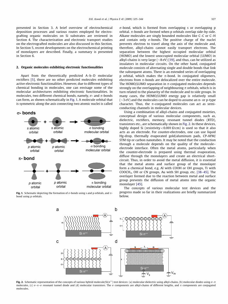
Apart from the theoretically predicted A–b–D molecularrectifiers [5], there are no other predicted molecules exhibitingactive electronic functionalities. However, due to different types ofchemical bonding in molecules, one can envisage some of themolecular architectures exhibiting electronic functionalities. Inmolecules, two different chemical bonds, namely, s- and p-bondscan form, as shown schematically in Fig. 1. A molecule orbital thatis symmetric along the axis connecting two atomic nuclei is called
Fig. 1. Schematic depicting the formation of s-bonds using s and p orbitals, and p-
bond using p orbitals.
Fig. 2. Schematic representation of the concepts of various hybrid molecule/Si(n++) test
molecules, (c) s–p–s resonant tunnel diode and (d) molecular transistors. The s com
molecules.
s-bond, which is formed from overlapping s or overlapping porbital. p-bonds are formed when p orbitals overlap side-by-side.Alkane molecules are singly bounded molecules like C–C or C–Hand contain only s-bonds. The positive charge of the nucleiprevents electron to travel along the axis of the molecule and,therefore, alkyl-chains cannot easily transport electrons. Theseparation between the highest occupied molecular orbital(HOMO) and the lowest unoccupied molecular orbital (LUMO) inalkyl-chains is very large (�8 eV) [19], and thus, can be utilized asinsulators in molecular circuits. On the other hand, conjugatedmolecule consists of alternating single and double bonds that linkthe subsequent atoms. There is an extended series of overlappingp orbital, which makes the p-bond. In conjugated oligomers,electrons from p-bonds are delocalized over the entire molecule.The HOMO/LUMO separation in p-conjugated molecules dependsstrongly on the overlapping of neighbouring p orbitals, which is inturn related to the planarity of the molecule and to side groups. Inmany cases, the HOMO/LUMO energy gap is relatively small(�3 eV) and the molecules can be doped to assume an n- or p-typecharacter. Thus, the p-conjugated molecules can act as semi-conducting channels in molecular devices.
Using a combination of alkyl-chains and conjugated moieties,conceptual design of various molecular components, such as,dielectric, rectifiers, memory, resonant tunnel diodes (RTD),transistors etc., are schematically shown in Fig. 2. In these devices,highly doped Si (resistivityo0.001O cm) is used so that it alsoacts as an electrode. For counter-electrodes, one can use liquidHg-drop, thermally evaporated gold/aluminum pads, CP-AFM/STM tip or carbon nanotubes. It may be noted that the conductionthrough a molecule depends on the quality of the molecule–electrode interface. Often the metal atoms, particularly whenthe counter-electrode is prepared using thermal evaporation,diffuse through the monolayers and create an electrical short-circuit. Thus, in order to avoid the metal diffusion, it is essentialthat the metal atoms and surface group of the monolayerform a chemical bond, e.g. Al with COOH or OH groups, Ti withCOOCH3, OH or CN groups, Au with SH group, etc. [38–45]. Theoverlayer formed due to the reaction between metal and surfacegroup prevents the diffusion of metal atoms into the organicmonolayer [45].
The concepts of various molecular test devices and theprogress made so far in their realizations are briefly summarizedbelow.
devices: (a) molecular dielectric using alkyl-chains, (b) molecular diodes using s–pponents are alkyl-chains of different lengths, and p components are conjugated

ARTICLE IN PRESS
D.K. Aswal et al. / Physica E 41 (2009) 325–344328
2.1. Molecular dielectrics and wires
The dielectric property of the alkyl-chain monolayers has beenwell established [4]. The electrical measurements of the orderedalkyl-chains sandwiched between two electrodes, as shown inFig. 2(a), have revealed that the current through alkyl-chainsfollows the usual distance-dependent exponential law predictedby the tunnel theory: I ¼ I0 exp(�bd), where d is the monolayerthickness and b is the distance decay rate. However, the reportedvalue of b lies in a wide range 0.5–1 A�1 [20]. The b value isrelated to the tunneling barrier height (f) at the molecule/electrode interface and to the effective mass (m*) of carriers in themonolayer using the expression: b ¼ a(m*/m0)1/2f1/2, where m0 isthe rest mass of the electron and a ¼ 4p(2m0e)1/2/h (e is theelectron charge and h is the Planck’s constant) [44,46]. Thus, awide variation in the b value is associated to different f values(2.5–4.5 eV), which arise due to variations in the quality ofSi/molecule and molecule/counter-electrode interfaces. Highvalues (4–4.5 eV) are generally reported when at least oneinterface is weak e.g. for physisorbed LB monolayers [47,48],monolayer mechanically contacted by conducting atomic forcemicroscope tip [49,50] or counter-electrode (Al or Au) weaklycoupled to monolayer [51,52]. Lower barrier heights (2.2–2.5 eV)have been obtained when both the interfaces are strong e.g. Aucounter-electrode on SH-terminated monolayer of alkyl-chainsgrafted on native oxide of Si [44,53]. Similarly, the reported valuesof m* have been found to vary in a wide range 0.16 me–1 me (me isthe mass of free electron). In order to understand the widevariation in m*, investigations on the electron–molecular vibrationcoupling need to be carried out. Other effects that might influencethe transport in an ordered monolayer include current-inducedlocal heating in a molecular junction [54], dynamical chargefluctuations [55] and spin-polarized transport [56,57]. If themonolayer is disordered or contains defects, the electronicconduction through the monolayer can take place by othermechanisms, such as, tunneling, thermionic emission, Poole–Frankel emission and/or hopping conduction. One can identify theresponsible mechanism by carrying out the temperature and biasdependences of the current density through monolayers, and thedetails of these mechanisms can be found in Ref. [2].
While alkyl-chains are proven to act as a dielectric, shortoligomers of p-conjugated molecules, such as, di(phenylene–ethynylene)benzenethiolate [58,59], terthiophene [59], shortconjugated oligomers [8–10,60,61], organometallic [62], porphyr-in-oligomer [63], etc. are considered as the prototype molecularsemiconducting wires. The J–V curves of such molecular wires arein general non-linear with steps (i.e. peaks in the first derivative),corresponding to resonant charge carrier transfer through themolecular orbitals of the molecules [64]. The measured con-ductance corresponds to the conductance through the moleculesand the conductance of the molecule/electrode contact. Thus, theinfluence of the chemical link between the molecules and theelectrode is of prime importance and requires further investiga-tions using different sets of molecule/electrode combinations.
2.2. Molecular diodes
Based on Aviram–Ratner (AR) A–b–D concepts of moleculardiode (as discussed in the introduction), several molecularrectifying diodes have been synthesized, e.g. hexadecylquinoli-nium tricyanoquinodimethanide molecule (C16H33–Q–3CNQ) withdonor and acceptor moieties linked by s- or p-bridge [6,65–70].Also, the molecule is o-substituted by an alkyl-chain, which isessential to allow a monolayer formation by the Langmuir–Blodgett (LB) method. These molecular diodes exhibited rectifica-tion ratio (a ratio of current density at �1 V (in absolute value)
and the current density at +1 V) up to 2�104. However, in the caseof C16H33–Q–3CNQ the AR model may not be applicable as it is aD–p–A molecule [68], and due to the p-bridge, the HOMO andLUMO may be more delocalized than expected in the AR model.Theoretical calculations show that the direction of easy currentflow (i.e. rectification current) depends on: (i) the placement ofthe HOMO and LUMO relative to the Fermi levels of the metalelectrodes before bias is applied and (ii) a shift induced in HOMO/LUMO by the applied bias. This situation is more complex than theAR mechanism and the electrical rectification can result from theasymmetric profile of the electrostatic potential across themolecule [71]. Thus, the rectification in the C16H33–Q–3CNQmolecule can be attributed to the asymmetry profile due to alkyltail. Prediction of a symmetric J–V curve in this molecule withoutan alkyl-chain also suggests that asymmetric electrostaticpotential is the cause for rectification in C16H33–Q–3CNQmolecule [72–75]. Based on the rectification due to asymmetricelectrostatic potential profile in a molecular system, experimen-tally a simple molecular rectifier with only one donor group andan alkyl spacer chain [76], as schematically shown in Fig. 2(b), hasbeen demonstrated. Such s–p molecular rectifiers with p-groups,such as, phenyl, pyrene, thiophene, anthracene, quaterthiophene(4 T), etc. coupled to alkyl-chains of different lengths have indeedbeen deposited on Si using a sequential self-assembly process.These s–p rectifiers have exhibited rectification ratio up to 37. Ithas been further demonstrated that the rectification in such s–pmolecular diodes occurs due to resonance through the HOMO ofthe p-group [76]. More emphasis is thus required to design s–pmolecular diodes with different p-groups so that high rectificationratios are obtained.
2.3. Molecular memories
Molecular memories have been designed employing threedifferent properties of the molecules, as discussed below
(i)
Resistive memory: the resistive memory or switch is based onthe electrical bistability (i.e. two different conduction statesfor same bias voltage) exhibited by the organic molecules.Electrical bistability has been reported in a number ofmolecules, such as, rotaxanes [77,78], catenanes [79], stearicacid [80], eicosanoic acid [81] and phenylene–ethynyleneoligomers [82–85]. In order to explain the observed switchingbehavior various proposals have been put forward. Theseinclude electrical charge transfer [86,87], molecular confor-mational change [83,85] and bond fluctuations between themolecule and their electrical contacts [88]. While theseefforts have demonstrated the basic functionality of aresistive molecular switch, there are several open questionsthat need to be answered. (i) Can the structure of moleculesexhibiting electrical bistability generalized? (ii) Will thecurrent controversy on the origin of molecular switching beresolved? (iii) Can molecular switches be made compatiblewith the technologically important silicon substrates?Clearly, in-depth experiments would be needed in future toanswer these questions.(ii)
Capacitive memory: in this case, one utilizes the differentredox states of a molecule. The capacitive memory works onthe principle of charging and discharging of the moleculesinto different chemically reduced or oxidized (redox) states[89–92]. Redox-active molecules, such as metallocene, por-phyrin and triple-decker sandwich coordination compoundsattached on a silicon substrate have been found to act ascharge storage molecular devices [90–92]. It has beendemonstrated that porphyrins: (i) offer the possibility ofmultibit storage at relatively low potentials (below 1.6 V); (ii)
ARTICLE IN PRESS
D.K. Aswal et al. / Physica E 41 (2009) 325–344 329
can undergo trillions of write/read/erase cycles; (iii) exhibitcharge retention times that are long enough (minutes)compared with those of semiconductor DRAM (tens of ms);and (iv) are extremely stable under harsh conditions(400 1C–30 min) and therefore meet the processing andoperating conditions required for the use in hybrid mole-cule/silicon devices [92].
(iii)
Resonant tunnel diodes (RTD): RTD memory utilizes thenegative differential resistance (NDR) behavior of moleculesin their J–V characteristics. The architecture of the molecularRTD device, as shown in Fig. 2(c), is analogous to its solid-state counter-part [93]: a potential well separated from theelectrodes by two tunnel barriers. Here alkyl-chains can actas tunnel barriers, while a p-moiety acts as the potential well.The advantages of RTD molecular memory compared to‘resistive’ and ‘capacitive’ molecular memories are fastswitching times and possible long-retention times. However,till date no success has been made in the s–p–s types ofmolecular RTDs. In literature, NDR behavior has beenreported using STM measurements carried on a singlemolecule attached to Si [94] and this effect has beenattributed to resonance through the molecular orbitals [95].However, this interpretation subsequently has been ruled outboth experimentally [96] and theoretically [97], indicatingthat RTD molecular device has not yet been demonstratedunambiguously. Thus, synthesis of new types of s–p–smolecules, suitable for grafting to Si, is required.2.4. Molecular transistors
The concept of molecular transistor, as shown in Fig. 2(d), isanalogous to the solid-state counter-part of the field-effecttransistor, which is a three-terminal device [93]. The source (S)and drain (D) electrodes, separated by a distance L, are depositedon semiconducting channel made from p-moieties. The alkyl-chains of length (t) act as gate dielectric (G). FETs are based on agate field modulating the conductance of the semiconductingchannel to turn the device ‘‘off’’ and ‘‘on.’’ Kagan et al. [98] haveinvestigated the chemical and physical requirements necessaryfor a successful design and fabrication of molecular FETs. Atheoretical analysis using electron tunnelling and device electro-statics place L42.5–3 nm and minimum gate dielectric thicknesst ¼ L/1.5 for such devices [98]. However, till date no molecular-FEThas been experimentally demonstrated. However, it has beenindependently demonstrated that (i) alkyl-chains work as gooddielectric materials in FETs made using sexithiophene- orpentacene-based organic thin film transistors (OTFTs) [99,101]and (ii) OH-functionalized tetracene self-assembled monolayerindeed works as an active channel of the transistor [101].However, in this case, a layer of aluminium oxide (�5 nm) wasutilized to act both as a dielectric layer and also as a primer for theassembly of the monolayer. Probably it is just a matter of timewhen true molecular transistors will be fabricated. One of thecritical requirements for making molecular transistors is avail-ability of p-molecules with exceptionally small (o0.5 eV)HOMO–LUMO gaps, which have now become syntheticallyachievable targets [102].
3. Hydrogen-terminated silicon surfaces
For electrochemical grafting, highly doped Si wafers (n-type ondoping with P or As, and p-type doping with B) of resistivityo0.001O cm are used as working electrodes. Since Si wafers arealways covered with native oxide, it is essential that this oxidelayer is removed and a clean hydrogen-terminated surface is
created. The hydrogen termination of Si surfaces is preparedeither by reaction of a clean surface with hydrogen atoms in UHVor by chemical etching in aqueous fluoride. For electrochemicalgrafting experiments the chemical etching process is adopted. Inliterature, Si(111) and Si(10 0) are the two surfaces on whichessentially all of the grafting has been carried out.
A simple wet chemical method for the preparation of atom-ically flat hydrogen-terminated Si(111) has been described byChabal and his co-workers [103,104]. They found that the HFetching of Si(111) at pH 8–9 or 40% ammonium fluoride results inthe formation of hydrogen-terminated Si(111) surfaces in whichthe Si–H bond is oriented normal to the surface as shown in Fig. 3.The observation of a single narrow line at 2083.7 cm�1 (the Si–Hstretch) with p-polarized infrared light (i.e. the electric fieldcomponent is perpendicular to the surface) and the absence ofthis vibration with s-polarized infrared light (i.e. the electric fieldcomponent is in the plane of the surface) provided unambiguousproof of the orientation of the Si–H bond. STM image showedformation of atomically flat Si(111) surfaces: a 3-fold symmetricarrangement of silicon atoms, separated by 0.384 nm, each cappedwith a hydrogen atom [105,106].
Because of the anisotropic nature of the ammonium fluorideetching of silicon, it is not possible to produce atomically flatH–Si(10 0) surfaces by chemical etching. In fact, chemical etchingof Si(10 0) surfaces tends to roughen the surface by exposingSi(111) facets leading ultimately to the formation of poroussilicon [107]. Using 2% HF it is possible to produce relativelyflat surfaces with small atomically resolved domains but thestructure of hydrogenated surfaces produced in this way are notuniform and contain some SiH and SiH3 groups but arepredominantly SiH2 [108]. Under UHV conditions it is possibleto produce uniform H–Si(10 0) surfaces. For this the Si (10 0)surface is first heated in UHV to obtain a clean surface (i.e. thesurface atoms are not chemically terminated but have so-calleddangling bonds protruding into space) followed by exposure tohydrogen atoms. The hydrogen-terminated silicon surfaces areactually quite stable and can be handled in air for several minuteswithout oxidation [109].
4. Electrochemical grafting of organic molecules
The electrografting of organic molecules to Si surface iscarried out using a three-electrode electrochemical setup, asschematically shown in Fig. 4. The current (I) flows between theworking electrode (WE) and the counter-electrode (CE). Theworking electrode is the electrode on which the molecules aregrafted, that is, H-terminated Si. The counter-electrode is usually aPt wire. The potential (V) is measured between the referenceelectrode (RE) and the working electrode. No current passesthrough the reference electrode. Reference electrode is anelectrode which has a stable and well-known electrode potential.The high stability of the electrode potential is usually reached byemploying a redox system with constant (buffered or saturated)concentrations of each participants of the redox reaction.Commonly used reference electrode is standard hydrogen elec-trode (SHE), which is also known as ‘‘normal hydrogen electrode’’(NHE). Other used reference electrodes are saturated calomelelectrode (SCE) (E ¼ +0.242 V with respect to the SHE), copper–copper (II) sulfate electrode (E ¼ 0.314 V) and silver chlorideelectrode (E ¼ 0.225 V saturated) [110,111]. The commonly usedsupporting electrolytes include tetrabutylammonium perchlorate(TBAP) or tetrabutylammonium hexafluorophosphate (TBAPF6)prepared in dry and deoxygenated dichloromethane (CH2Cl2)or acetonitrile (CH3CN). To avoid oxidation of the H-terminated Sisurface, the electrografting process is generally carried under

ARTICLE IN PRESS
Fig. 3. Schematic representation of the formation processes of H-terminated (a) Si(111) and (b) Si(10 0) surfaces.
Fig. 4. Schematic drawing of a three-electrode electrochemical setup. The current
flows between the counter-electrode (CE) and the working electrode (WE). The
molecules are deposited on the working electrode. The potential is measured
relative to the reference electrode (RE).Fig. 5. (a) Molecular structure of 5-(4-undecenyloxyphenyl)-10,15,20-triphenyl-
porphyrin (TPP-C11) [112]. (b) CV runs recorded using the TPP-C11+TBAP solution.
The inset shows CV runs using the C11+TBAP solution [112].
D.K. Aswal et al. / Physica E 41 (2009) 325–344330
inert ambient. The electrografting is usually carried out usingeither cyclic voltammetry (CV) (i.e. the working electrodepotential is ramped linearly versus time) or constant appliedpotential mode.
Once the electrografting reaction has been achieved, it isessential to ascertain the presence of the organic layer on the Sisurface. For this purpose, the electrografted Si is thoroughlyrinsed ultrasonically, so that all physisorbed molecules areremoved from the surface and only chemically bonded moleculesremain on the surface. In order to prove the presence of theattached monolayer, a number of electrochemical and spectro-scopic techniques are used. The characterization of organicmonolayers typically involves a combination of multiple techni-ques, such as, ellipsometry, water contact angle measurement,Fourier transform infrared spectroscopy (FTIR), X-ray photoelec-tron spectroscopy (XPS), atomic force microscopy, etc. Forchemical analysis, FTIR is commonly used. The frequencies andintensities of the vibrational modes observed in FTIR providedetailed information about the nature of the chemical functionalgroups. The XPS technique provides excellent information aboutthe elements and their oxidation states present in the monolayer.In addition, XPS allows determination of thickness of the graftedorganic layers. Thickness of the organic layers can also bedetermined using ellipsometry. Contact angle measurementsprovide information on the surface group of the grafted organiclayer [2]. The ordering of the monolayer can be assessed byimaging the morphology of the organic layers using AFM andSTM. In order to measure the electronic transport of the graftedorganic layers, counter-electrodes, such as, liquid Hg-drop,thermally evaporated gold pads, CP-AFM or STM tip or carbonnanotube, as shown in Fig. 2, are used to fabricate a metal/monolayer/ Si(n++) structure.
4.1. Terminal vinyl (CQC) as reactant
Alkene-1 and vinyl-terminated derivatives of molecules, forexample, 5-(4-undecenyloxyphenyl)-10,15,20-triphenylporphyrin(TPP-C11), have been deposited on doped n-Si substrates by anelectrochemical process via formation of Si–C bonds [112]. Themolecular structure of TPP-C11 molecule is shown in Fig. 5(a). Itconsists of a vinyl (CQC)-terminated 11-carbon atom alkyl-chainattached to the conjugated porphyrin ring. The monolayers of1-undecene (C11) and TPP-C11 were deposited on H-terminated Si(111) by CV using a solution containing 1:1 (v/v) of 0.1 M TBAPsupporting electrolyte and 1 mM C11 or TPP-C11 in dry CH2Cl2.
Typical CV scans recorded using TPP-C11+TBAP and,1-undecene (C11)+TBAP solutions are shown in Fig. 5(b), whichare nearly identical. It is seen that the presence of an irreversibleoxidation peak at �0.3 V, observed for the first scan, disappearsrapidly as the number of scans increased and, eventually vanishesfor 50th scan. However, no peak at �0.3 V appeared when the CVwas run using the TBAP solution alone. The fact that thevoltammetric peak is irreversible, indicates that an irreversiblereaction (i.e. the cleavage of vinyl-group) is associated with theelectron transfer. Disappearing of the peak with increased cyclesis indicative of the blocking of the surface by the molecules(TPP-C11 or C11), which become attached to the H-terminatedSi surface.
The proposed electrochemical reaction of the grafting ofmolecules is shown in Fig. 6, which takes place in several steps.In the first step, application of a negative potential to the workingelectrode (H-terminated Si) makes Si radical atoms at the surfaceby releasing hydrogen hydride (Fig. 6(a)). These anions ontransferring from electrode to the electrolyte solution generate
ARTICLE IN PRESS
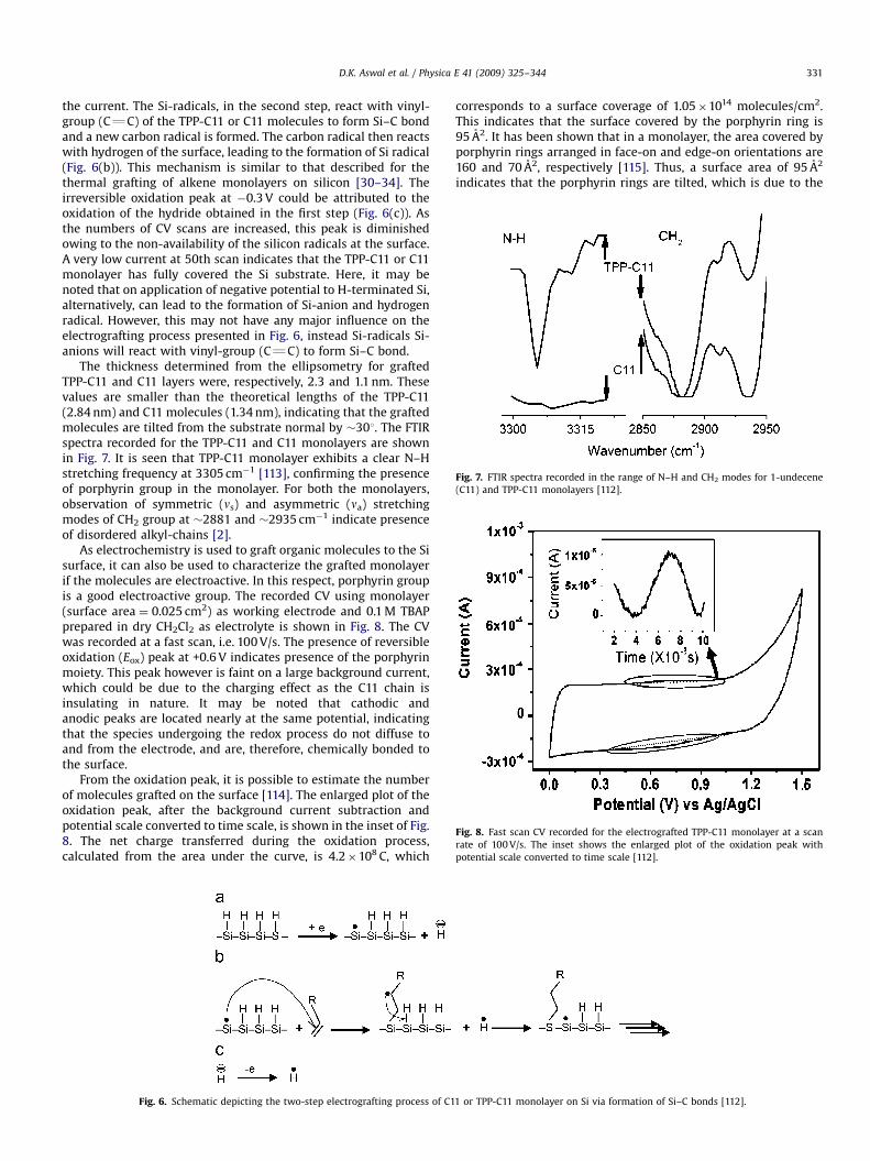
Fig. 7. FTIR spectra recorded in the range of N–H and CH2 modes for 1-undecene
(C11) and TPP-C11 monolayers [112].
Fig. 8. Fast scan CV recorded for the electrografted TPP-C11 monolayer at a scan
rate of 100 V/s. The inset shows the enlarged plot of the oxidation peak with
potential scale converted to time scale [112].
D.K. Aswal et al. / Physica E 41 (2009) 325–344 331
the current. The Si-radicals, in the second step, react with vinyl-group (CQC) of the TPP-C11 or C11 molecules to form Si–C bondand a new carbon radical is formed. The carbon radical then reactswith hydrogen of the surface, leading to the formation of Si radical(Fig. 6(b)). This mechanism is similar to that described for thethermal grafting of alkene monolayers on silicon [30–34]. Theirreversible oxidation peak at �0.3 V could be attributed to theoxidation of the hydride obtained in the first step (Fig. 6(c)). Asthe numbers of CV scans are increased, this peak is diminishedowing to the non-availability of the silicon radicals at the surface.A very low current at 50th scan indicates that the TPP-C11 or C11monolayer has fully covered the Si substrate. Here, it may benoted that on application of negative potential to H-terminated Si,alternatively, can lead to the formation of Si-anion and hydrogenradical. However, this may not have any major influence on theelectrografting process presented in Fig. 6, instead Si-radicals Si-anions will react with vinyl-group (CQC) to form Si–C bond.
The thickness determined from the ellipsometry for graftedTPP-C11 and C11 layers were, respectively, 2.3 and 1.1 nm. Thesevalues are smaller than the theoretical lengths of the TPP-C11(2.84 nm) and C11 molecules (1.34 nm), indicating that the graftedmolecules are tilted from the substrate normal by �301. The FTIRspectra recorded for the TPP-C11 and C11 monolayers are shownin Fig. 7. It is seen that TPP-C11 monolayer exhibits a clear N–Hstretching frequency at 3305 cm�1 [113], confirming the presenceof porphyrin group in the monolayer. For both the monolayers,observation of symmetric (ns) and asymmetric (na) stretchingmodes of CH2 group at �2881 and �2935 cm�1 indicate presenceof disordered alkyl-chains [2].
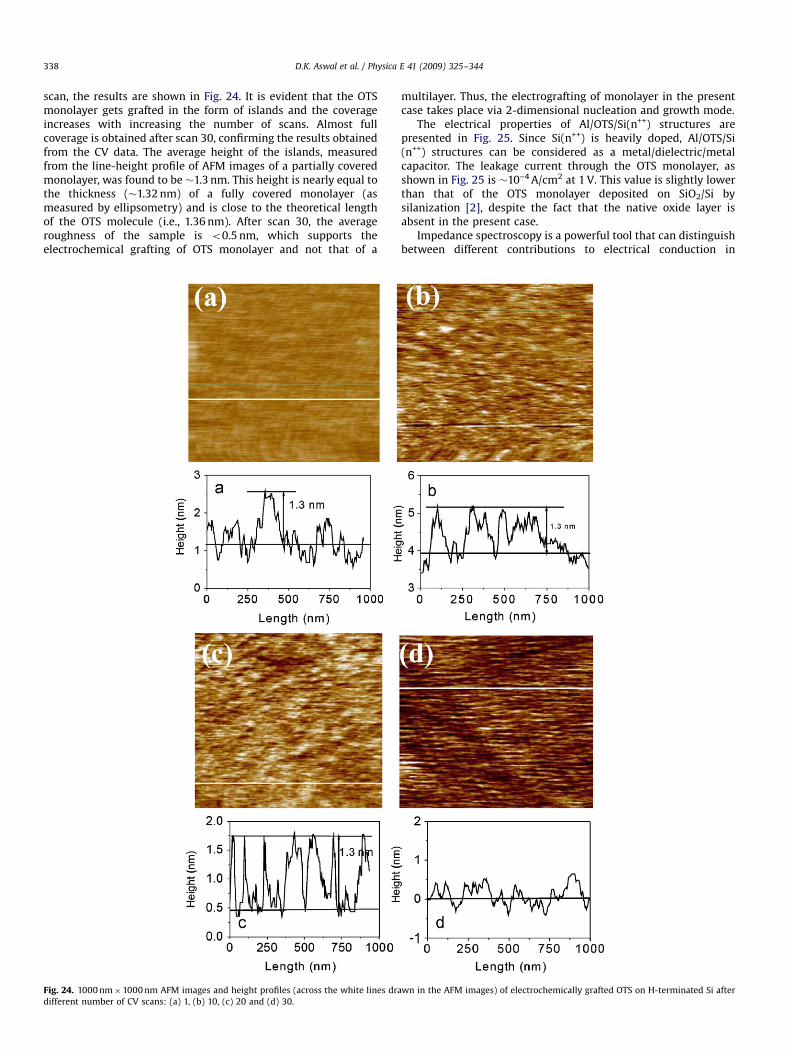
As electrochemistry is used to graft organic molecules to the Sisurface, it can also be used to characterize the grafted monolayerif the molecules are electroactive. In this respect, porphyrin groupis a good electroactive group. The recorded CV using monolayer(surface area ¼ 0.025 cm2) as working electrode and 0.1 M TBAPprepared in dry CH2Cl2 as electrolyte is shown in Fig. 8. The CVwas recorded at a fast scan, i.e. 100 V/s. The presence of reversibleoxidation (Eox) peak at +0.6 V indicates presence of the porphyrinmoiety. This peak however is faint on a large background current,which could be due to the charging effect as the C11 chain isinsulating in nature. It may be noted that cathodic andanodic peaks are located nearly at the same potential, indicatingthat the species undergoing the redox process do not diffuse toand from the electrode, and are, therefore, chemically bonded tothe surface.
From the oxidation peak, it is possible to estimate the numberof molecules grafted on the surface [114]. The enlarged plot of theoxidation peak, after the background current subtraction andpotential scale converted to time scale, is shown in the inset of Fig.8. The net charge transferred during the oxidation process,calculated from the area under the curve, is 4.2�108 C, which
Fig. 6. Schematic depicting the two-step electrografting process of C1
corresponds to a surface coverage of 1.05�1014 molecules/cm2.This indicates that the surface covered by the porphyrin ring is95 A2. It has been shown that in a monolayer, the area covered byporphyrin rings arranged in face-on and edge-on orientations are160 and 70 A2, respectively [115]. Thus, a surface area of 95 A2
indicates that the porphyrin rings are tilted, which is due to the
1 or TPP-C11 monolayer on Si via formation of Si–C bonds [112].

ARTICLE IN PRESS
Fig. 10. Reproducible J–V characteristics exhibiting hysteresis recorded for a TPP-
C11 monolayer. Upper inset shows J–V characteristics recorded for C11 monolayer.
Lower inset shows schematic of the device structure [112].
Fig. 11. Demonstration of the memory effect in TPP-C11 monolayers. Dotted lines
are guide to eye to distinguish between ‘read’ currents (measured at 0.5 V) after
application of ‘write’ (0 V) and ‘erase’ (0.8 V) pulses [112].
D.K. Aswal et al. / Physica E 41 (2009) 325–344332
fact that alkyl-chains are tilted by 301 from the substrate normal.A densely packed monolayer, as shown in Fig. 9, has also beenobserved by atomic force microscopy.
To measure J–V characteristics of the monolayers, a metal/monolayer/Si(n++) structure was completed by using a very smalldrop of liquid mercury as a counter-electrode. Typical J–V plotsrecorded for TPP-C11 and C11 monolayers are shown in Fig. 10.J–V0s are slightly asymmetric, which is attributed to the differentwork functions of the electrodes, i.e. Si (4.1 eV) and Hg (4.5 eV)[42]. It may be noted that the J–V0s of C11 monolayer do notexhibit any hysteresis; whereas for TPP-C11 monolayer a pro-nounced hysteresis is observed, indicating a predominant roleplayed by porphyrin ring. In the positive bias scan, i.e. from 0 to+0.8 V, current jumps by an order of magnitude at +0.6 V.However, on the reverse scan (+0.8–0 V) the current does notretrace the curve, and remains at higher values. Thus, the J–V inthe voltage range �0.6 V to +0.6 V exhibits two conduction states:one with low current (OFF) and other with higher current (ON).
The electrical bistable behavior of TPP-C11 molecules has alsobeen demonstrated for molecular memory effects. The memoryphenomenon in electrically bistable devices is best demonstratedunder ‘write–read–erase–read’ operations. In such a sequence ofcycles, the low-conducting (‘write’) and high-conducting (‘erase’)states are induced repeatedly and the states are monitored (‘read’)in between. In the present case, 0 and +0.8 V pulses for 10 s wereapplied, respectively, to ‘write’ the low-conducting state and‘erase’ the high-conducting one. These states were continuouslymonitored (‘read’) by measuring the device current (at 0.5 V), formore than 50 reading operations, and a section of ‘write–read–erase–read’ operation recorded for such a device is shown inFig. 11. The magnitude of the device current under the ‘read’voltage pulse is �130% higher for high-conducting state (‘erase’)as compared to that for low-conducting state (‘write’). Theobserved change in current for these devices is far superior thanthat reported recently (�30%) for memory devices fabricatedusing oligo(phenylene–ethynylene) molecules [80].
Electrografting of other vinyl-group-terminated molecules,such as, N-succinimidyl acrylate (NSA), on Si substrates has alsobeen demonstrated in literature [116]. The NSA-modified Sielectrodes were immersed in isopropylamine in order to trans-form the grafted chains to the thermoresponsive poly(N-isopropylacrylamide), which are promising for microfludics application.However, the electronic transport properties of NSA layers havenot been investigated.
Fig. 9. 500 nm�500 nm AFM image and height profile of the TPP-C11 monolayer electrografted on Si(111). The average surface roughness is o1 nm.

ARTICLE IN PRESS
Fig. 13. Two different proposed electrografting mechanisms of organic molecules
to Si using alkyl halides (after Ref. [126]).
D.K. Aswal et al. / Physica E 41 (2009) 325–344 333
4.2. Terminal ethynyl (CRC) as reactant
Buriak et al. [117] have reported a cathodic electrograftingprocess that directly attaches alkynes to the porous Si surface. Theelectrografting was carried out using a solution of alkyne mixedwith 0.1 M tetrabutylammoniumhexafluorophosphate electrolytein CH2Cl2. A current of �10 mA is then applied typically for 120 s.Later, the sample is gently washed with CH2Cl2/pentane and driedunder a nitrogen stream. FTIR analysis of electrografted phenyla-cetylene reveals Si–Hx stretches, which are broadened anddecreased in integrated intensity compared to unmodified poroussilicon. The absence of a n(RCH) mode around 3300 cm�1 and anobserved sharp silylated alkyne n(CRC) at 2159 cm�1 is consis-tent with a Si–alkynyl surface and not simple physisorption. It hasbeen proposed that the cathodic electrografting reaction ofalkynes proceeds via a silyl anion intermediate formed byreduction of surface Si–H bonds in a space charge layer[118,119], as shown in Fig. 12. The subsequent in situ generationof a carbanion from deprotonation of the weakly acidic alkyneleads directly to nucleophilic Si–Si bond attack [120,121].
Cathodic electrografting of hexynoic acid, CHRC–(CH2)3–COOH, to silicon nanowire surfaces has also been reported [122].The electrografting mechanism in this case is expected to besimilar to that presented in Fig. 12. Carboxylic acid-terminated(�COOH) alkane monolayers have also been covalently anchoredon Si by cathodic electrografting with a terminal alkyne asreactant [123,124]. For comparison, monolayers have also beengrafted using heat- or light-promoted chemical reactions. It hasbeen demonstrated that cathodic electrografting produces thebest-quality monolayers. Moreover, it is worth to recall thatduring cathodic electrografting silicon is normally protectedagainst oxide (SiO2) growth, which is instead enhanced inphotochemical and mostly in thermal processes.
Covalent bonding of alkynes to Si using anodic electro-grafting has also been reported [117]. The anodic electrograftedsurfaces show a complete reduction of all unsaturated bonds.The results of FTIR revealed that a surface-initiated cationichydrosilylation mechanism is responsible for the Si–C bondformation in anodic electrografting. Positive charges are stabilizedin the depletion layer at the semiconductor–electrolyte interface,which are attacked by alkyne monomers. This can then bethe starting point for a successive hydrosilylation or cationicpolymerization reaction. It may be noted here that anodisationof silicon in the presence of water unavoidably leads to theformation of a layer of silicon dioxide, or, in the case offluoride electrolytes, to the dissolution of silicon [125]. If anorganic modification of Si is desired by anodic electrogarfting,it is essential that the process must be carried out underrigorously anhydrous and oxygen-free conditions. Thus, dueto potential risk of the oxidation of Si, anodic electrogafting isnot a very suitable process for making monolayers for hybridnanoelectronics.
Fig. 12. Proposed mechanism for the cathodic electrografting of alkynes to silicon. Cath
the reaction (after Ref. [117]).
4.3. Terminal halide as reactant
The electrochemical grafting of molecules on H-terminated Sisurfaces has also been reported using reductive electrolysis ofalkyl halides mainly iodides [126]. The reductions have beenperformed in 0.2–0.4 M solutions of the organo halides in dry,deoxygenated acetonitrile or mixtures of acetonitrile and tetra-hydrofuran containing 0.2 M LiBF4. Alkyl/benzyl bromides, whichdo not graft, were converted into the iodides in situ by replacingLiBF4 with LiI as the electrolyte. Passing a cathodic current(2710 mAcm�2) for short periods of time (307120 s) resulted in ahigh coverage of the silicon surface with organic species, asdetermined by FTIR i.e. appearance of the Si–C stretching mode inthe infrared spectrum at 766 cm�1 [127]. Also, the integratedintensity of the Si–H stretching vibrations, located at approxi-mately 2120 cm�1, decrease substantially with increasing alkylcoverage. This suggests that the reduction produces alkyl orbenzyl radical species that then react with the hydrogen-terminated surface to form radical silicon. The electrograftingprocess may occur by two different routes as schematically shownin Fig. 13. In the first route, the reduction process produces alkylradical, which then directly reacts to the surface silicon radical,Fig. 13(a). The second route would be through the reduction of thesilicon radical to the anion followed by nucleophilic attack on theorganohalide, Fig. 13(b). The grafted alkyl layers were found to bestable in boiling chloroform, aqueous ethanolic HF and 0.1 M KOHas demonstrated by the difference between contact anglesmeasured on grafted and nongrafted surfaces, respectively.
Monolayers of 2,20-bipyridines have been prepared by cathodicelectrografting on H-terminated n- and p-Si (10 0) surfacesusing a solution of 5-bromomethyl-2,20-bipyridine [128]. Themonolayers of 2,20-bipyridines were also prepared by twoother methods namely, photochemical reaction of 5-vinyl-2,20-
odic reduction of a surface Si–H group forms the active silyl anion, which initiates

ARTICLE IN PRESS
D.K. Aswal et al. / Physica E 41 (2009) 325–344334
bipyridine and thermal reaction of 5-vinyl-2,20-bipyridine. It hasbeen demonstrated that cathodic electrografting resulted in themost satisfactory anchoring procedure, because of its bettercorrelation between high coverage and preservation of the Sisurface from both oxidation and contamination.
4.4. Tetraalkylammonium salts
The cathodic alkylation of H-terminated silicon surfaces hasbeen reported using 0.1 M ammonium (or phosphonium/pyridi-nium) salt solution in dichloromethane by passing a cathodiccurrent (typically 10 mA cm�2) [129]. AFM scribing of covalentlymodified surfaces has been used to provide measurements of thethickness of the grafted layers [130]. First, the surface was imagedat contact mode with minimized force (less than 5 nN). Then, theAFM tip was pushed to scratch the surface with a force of 200 nNin a zoomed area. The corresponding control experiment on anH-terminated Si surface is also carried out to ensure that this forcedoes not significantly damage the underlying silicon. Finally, thearea was imaged with minimized force, and from the height of thetrench thickness of the grafted layer is estimated. It has beenshown that the trench was 1.4 nm deep, which corresponds to theapproximate length of the dodecyl group indicating the grafting ofa monolayer. XPS data indicated that surface oxidation of Si doesnot occur, and no nitrogen arising from the ammonium saltprecursor remains in the film. FTIR spectra show the presence ofsymmetric CH2 at 2923–2924 cm�1, indicating some disorder inthe grafted alkyl-chains. The two mechanistic pathways by whichthe alkylation reaction could proceed are shown in Fig. 14. Themechanism starts with the reduction of the tetraalkylammoniumNR4 cation, which decomposes into R radical and NR3. Subse-quently, the R radicals lead to radical-based surface alkylation. Ina first pathway the silicon radical reacts with another R radical,Fig. 14(a). In the second possible route, formation of silyl anionsunder the cathodic conditions on the surface could be followed bynucleophilic attack on the trialkylammonium cation, Fig. 14(b),which is similar to the halides reaction (see Fig. 13).
Fig. 14. The two possible mechanistic pathways for alkylation of Si surfaces (after
Ref. [129]).
4.5. Diazonium and iodonium salts
The grafting of organic molecules to Si surface using electro-chemical reduction of diazonium is a very simple process[131–133]. A diazonium salt (BF4
� +N2ArR, where Ar and Rrepresent benzene ring and a functional group, respectively) oftypical concentration 1–10 mM is dissolved in an aprotic mediumwith a supporting electrolyte (ACN+0.1 M NBu4BF4) or in acidicaqueous medium (for example H2SO4 0.1 M). The diazonium salt isthen reduced using H-terminated Si as a cathode, which results inthe grafting of ArR molecules to Si surface. The grafting can becarried out in CV mode or by applying a constant potential(determined from the voltammetric reduction peak of thediazonium) for a variable period of time, typically few tens ofseconds. The H-terminated Si is then rinsed in an ultrasonic bathin order to remove physisorbed molecules. This approach, apartfrom Si, has been used to graft molecules on different substrates,such as, carbon (GC, HOPG, pyrolized photoresists, pyrolizedTeflon, carbon fibers, carbon blacks, carbon nanotubes, diamond,etc.) [134–142], semiconductors (GaAs) [143] and metals (Au, Cu,Fe, Ni, Pt, Pd, etc.) [144–146].
Here, we describe the electrografting of a specially synthesizeds–p–s molecule, that is, N-(2-(4-diazoniophenyl)ethyl)-N0-hexylnaphthalene-1,8:4,5-tetracarboxydiimide tetrafluoroborate(DHTT) to the Si using its diazonium salt. The molecular structureof this molecule is shown in Fig. 15 and the length of this moleculeis 2.06 nm. Typical cyclic voltammogram of this diazonium saltrecorded using H-terminated Si(111) as working electrode andACN+0.1 M TBAPF6 as electrolyte is shown in Fig. 16. The CV showsan irreversible peak at �0.66 V/Ag,Ag+, which shifts continuously tohigher values with increasing cycles (e.g. �0.69 V for fourth cycle).The presence of an irreversible reaction indicates cleavage ofdinitrogen, and hence a covalent reaction between H-terminatedSi and the molecule through an electron transfer mechanism.If there would have been formation of only a dense andimpervious monolayer then one had expected the disappearanceof the diazonium reduction peak during second cycle, as has beenreported for 4-nitrobenzene diazonium tetrafluoroborate [132].Disappearing of the diazonium reduction peak during secondcycle is indicative of the blocking of the H-terminated Si surfacewith covalently grafted monolayer. However, in the present case,the diazonium reduction peak does not vanish with successivecycles and, in fact, shifts to higher potentials. This indicates thatthe density of grafted molecules is not high enough in the firstcycle (i.e. making free H–Si surface available), which duringsubsequent cycles allows further electron transfer even if thediazonium salt reduces on the already grafted molecules. Thisprocess, therefore, results in the formation of highly branched orreticulated multilayer.
Let us now discuss possible reduction mechanisms of diazo-nium salts at silicon electrode that lead to the formation of themono- or/and multilayers [135]. The monolayer formation processis schematically demonstrated in Fig. 17(a). The phenyl radical isproduced directly ‘‘on the electrode’’ through an electron transfer
Fig. 15. Molecular structure of a diazonium salt of a s–p–s molecule namely, N-
(2-(4-diazoniophenyl)ethyl)-N0-hexylnaphthalene-1,8:4,5-tetracarboxydiimide
tetrafluoroborate (DHTT).

ARTICLE IN PRESS
D.K. Aswal et al. / Physica E 41 (2009) 325–344 335
concerted with the cleavage of dinitrogen to give the phenylradical. The aryl radical then causes abstraction of the hydrogenfrom the Si surface and moves away from the surface. The silylradical then reacts with a second aryl radical, which results in theformation of aRSi–ArR bond, and hence formation of the firstmonolayer. However, other aryl radical might attack the graftedaromatic group of the monolayer, as schematically shown InFig. 17(b), to form a bilayer. Repetition of this reaction would leadto the formation of the multilayers [147]. Since the attachment ofsubsequent molecules occurs randomly, the multilayers grown inthis way are expected to be inhomogeneous in thickness.
In order to ascertain the presence of mono- or multilayer onthe Si after the diazonium reduction process, the electrochemistrywas carried out after thorough ultrasonic rinsing. Using grafted
Fig. 17. The possible formation mechanisms of (a) monolayer and (b) multilayers on H-
-0.8-2x10⁻⁴
-1x10⁻⁴
-5x10⁻⁵
0
5x10⁻⁵
1x10⁻⁴
2x10⁻⁴
1
Cur
rent
(A)
Potential (V) vs Ag/Ag+
4
-0.6 -0.4 -0.2 0.0
Fig. 16. CV recorded using diazonium salt of s–p–s molecules using H-terminated
Si (111) as working electrode. Note the shift in the irreversible peak to higher
potentials with increasing number of scans.
layer as the working electrode, the CV was recorded in a solutioncontaining only the solvent and supporting electrolyte(CH2Cl2+0.1 M TBAPF6). As shown in Fig. 18, CV exhibits tworeversible peaks—which are the signature of the molecules—
with cathodic and anodic peaks being nearly at the samepotential, confirming grafting of the molecules to the Si surface.Similarly, other electrochemically active reporting groups, such as,4-bromophenyl, 4-cyanophenyl, 4-phenylazophenyl, naphthyl,anthraquinone, 4-benzoylphenyl, have been used to demonstratethe presence of the grafted organic layer [135]. The FTIR data toohas confirmed the presence of the molecules on the surface. FTIRalso allows the demonstration of the fact that the diazonium saltsare not merely adsorbed on the surface through the absence of the+N2 stretching, which should be located in the 2300–2130 cm�1
terminated Si surfaces using the electrochemical reduction of the diazonium salts.
Fig. 18. CV recorded for the electrografted organic layers on Si grafted using the
reduction of diazonium salt.

ARTICLE IN PRESS
D.K. Aswal et al. / Physica E 41 (2009) 325–344336
region [138,148]. Further evidence indicating the formation of acovalent bond between the substrate and the organic layer comesfrom the strength of this bond, which resists ultrasonic cleaning ina variety of solvents (ACN, dimethylformamide, dimethyl sulf-oxide, benzene, benzonitrile, acetone, methanol, ethanol, dichlor-omethane and chloroform for 15 min each) [134]. On Si,4-bromophenyl layers resisted 40% HF for 2 min and 10 M NH4Ffor 1 min [131–133].
In order to measure, the electronic transport through the layersof the s–p–s molecules, an In–Ga eutectic liquid drop was kept onthe top of the layer. Upon varying the potential between the In–Gaon top of the monolayer and Si at the bottom, the J–V’s wererecorded. It may be noted that the samples prepared using p3cycles exhibited electrical shorts, indicating the formation ofinhomogeneous film. The samples prepared using 4 or morecycles were thick and many of them did not exhibit electricalshorts. However, as expected from the formation mechanism ofthe multilayer, these samples exhibited rough and non-uniformmorphology. The average thickness of a sample prepared using6 CV runs, as measured using elliposmetry, was �12 nm, indicat-ing more than 6 layers of the s–p–s molecules. Also, themeasured water contact angle was �801, which indicated thatthe alkyl-chains are disordered and/or some of the p-moieties ofthe molecules are exposed to the surface. For CH3-terminatedsurface of an ordered monolayer, the expected water contact angleis �1101 [2]. Therefore, making monolayers of s–p–s moleculeson Si using diazonium salts does not appear to be very easy. Atypical J–V recorded for a 12 nm thick s–p–s multilayer is shownin Fig. 19. The J–V exhibits very small NDR effects in both positiveand negative bias with peaks occurring at +1.2 and �1.6 V,respectively. Also the hysteresis is very little. The observation ofvery small NDR effect is attributed to the loss of s–p–s characterowing to the formation of an inhomogeneous multilayer. Thesestudies show that in order to achieve pronounced NDR effect it isessential that ordered s–p–s monolayers are grafted, and thispossibly can be achieved by controlling several parameters, suchas, grafting potential, electrolysis time or number of scans andconcentration of the diazonium salt.
Fig. 19. Current–voltage characteristic of the s–p–s layers grafted on Si using
diazonium salt.
The most interesting result concerning monolayers obtainedby reduction of diazonium salts was reported by Allongue et al.[131,132]. By controlling the charge consumed during theelectrolysis and by choosing the electrolysis potential at the peakpotential, they obtained an organized phenyl monolayer on H-terminated Si(111). STM images of the monolayer show 5�5 nm2
domains of organized molecules with a rectangular 3.8�6.5 A2
unit cell, which corresponds to a (1�ffiffiffi
3p
)R 301 modification ofthe Si(111) unit cell. It is somewhat surprising to observe anorganization of the aryl groups as once they are bonded to thesurface they cannot move and therefore cannot reorganize.However, formation of organized domains is possible if there isa higher probability of grafting a molecule in the neighbourhoodof a first attached molecule than far from this molecule. This couldbe due to stacking interactions of the aromatic molecules. Othergroups obtained different morphologies and thickness of thesamples prepared using reduction of diazonium salts. Forexample, 4-diethylaminophenyl groups grafted on HOPG surfacesrevealed a continuous layer with protruding features having aheight of nearly 8 nm [137]. Very thick layers (up to a thickness of100 nm) of 4-nitrophenyl groups were obtained by scanning thepotential for 20 cycles. Summing up, using diazonium salts,making monolayers is not very easy, as the multilayer formationtakes place quickly. However, in a recent paper, it has beenspeculated that multilayer formation can be prevented if onehinders certain positions of the diazonium ion [149]. It has beendemonstrated that if methyl group occupies 2- and 6-positions ofgrafted phenyl ring then further grafting does not occur andresults in the formation of a monolayer.
Electroreduction of diazonium salts has also been used as amask-free technique to pattern homogeneous Si electrodes withlocal doping [150,151]. In this case, silicon substrate is locallydoped in a desired pattern. It has been demonstrated that theunderlying doping directs the electrografting of polymer filmpreferentially over the doped areas of the substrate. However, thispatterning process is not suitable for hybrid nanoelectonicsbecause of the following two reasons: (i) the grown film isusually quite thick and (ii) due to presence of intrinsic silicon(high resistivity), the measurement of the transport properties ofthe electrografted layer is not easy.
An electrografting method of forming covalent bonds directlyto silicon hydride has also been demonstrated with the use ofiodonium salt precursors [152]. Grafting on H-terminated Sisurface has been accomplished by applying a negative bias of 2 V.Several molecules ranging from electron-deficient to electron-richhave been electrografted in this fashion. It has been shown thatthe electron-rich iodonium salts assemble as thicker films ascompared to the electron-deficient iodonium salts. However,the understanding of this trend requires more experiments.The proposed mechanism of electrografting is analogous to theattachment of diazonium salts to hydride-terminated siliconsurfaces, as discussed in Fig. 17. In the first step of the reactionmechanism, an electron is transferred from the surface of thesilicon to the iodonium salt. A cleavage of the carbon iodine bondwould result in a radical and iodobenzene. The radical can then becombined with the surface forming a Si-C bond.
4.6. Silanes
The electrochemical grafting of organic molecules on Sidescribed in previous sections has been via the formation ofSi–C bonds between Si and organic molecule. It has also beendemonstrated that electrochemical process allows grafting ofsilane molecules on Si via formation of Si–Si bonds [153]. Theoctyltrichlorosilane (OTS) monolayer on H-terminated Si was

ARTICLE IN PRESS
D.K. Aswal et al. / Physica E 41 (2009) 325–344 337
deposited in the CV mode under high-purity argon gas. CV wascarried out using a solution containing 1:1 (v/v) of 0.1 M TBAPsupporting electrolyte and 5 mM OTS in dry methanol. Controlexperiments were also carried out using TBAP solution alone.
Representative CV’s recorded using OTS+TBAP and TBAPsolutions alone are shown in Fig. 20. The variations in the valueof current at �1 V (measured from data of Fig. 21) with number ofscans are plotted in Fig. 21. It is seen that for TBAP solution thecurrent is very small (�10–6 A) and is nearly independent of thenumber of scans. On the other hand, for OTS+TBAP solutionthe current is very high (10–3 A) for scan 1, which decreasesexponentially to �10–5 A for scan 30 (a decrease of nearly twoorders in magnitude). Since TBAP is the supporting electrolyte,a very low current implies that there is no chemical reactionbetween the H-terminated Si working electrode and TBAPmolecules, and, therefore, no electrochemical grafting of TBAPmolecules takes place. On the other hand, a very high current forOTS+TBAP solution suggests that an electrochemical reactiontakes place between H-terminated Si working electrode and OTSmolecule. A possible electrochemical reaction, taking place in two
0
-2.0x10⁻³
-1.5x10⁻³
-1.0x10⁻³
-5.0x10⁻⁴
0.0
5.0x10⁻⁴
0
0
20
40
60
80
100
Cov
erag
e (%
)
Number of scans
Cur
rent
(A)
No. of scans
TBAP + OTS
TBAP
5 10 15 20 25 30
5 10 15 20 25 30
Fig. 21. Variation of current at �1 V as a function of the number of CV scans. Inset
shows coverage (%) of the OTS monolayer on H-terminated Si as a function of the
number of CV scans [153].
-1.2
-2.0x10⁻³
-1.5x10⁻³
-1.0x10⁻³
-5.0x10⁻⁴
0.0
-1.2
-1.0x10⁻⁵
-5.0x10⁻⁶
0.0
5.0x10⁻⁶
2010
1
Cur
rent
(A)
Voltage (V)
TBAP
5
Scan
scan30scan25
scan20scan15
scan10
scan5Cur
rent
(A)
Voltage (V)
scan1
-1.0 -0.8 -0.6 -0.4 -0.2 0.0
-0.9 -0.6 -0.3 0.0
Fig. 20. Cyclic voltammograms recorded using TBAP+OTS electrolyte solution in
the potential range between 0 and �1 V at a scan rate of 0.05 V s–1 for different
numbers of scans. H-terminated Si was used as a working electrode. Inset shows
the CVs using TBAP solution [153].
steps, is shown in Fig. 22. In the first step, application of a negativepotential to the working electrode makes ‘‘nucleophilic Si’’ atomsat the surface by releasing hydrogen-free radicals. These nucleo-philic Si atoms, in the second step, then can react with‘‘electrophilic Si’’ atoms of OTS molecule to form Si–Si bond, andin the process chloride ions are released [153].
The OTS/Si interface was examined by recording the XPSspectra. The Si-2p spectrum, as shown in Fig. 23, exhibited thepresence of a single peak at �99 eV (Si–Si bonding) [154]. Fromthese data though it is difficult to distinguish the Si–Si bonding ofSi/OTS from that of the Si substrate itself; the absence of a peak at103 eV expected for oxide indicates that SiOx layer does not existbetween Si and OTS monolayer. In addition, no peaks correspond-ing to the Cl (expected in the event of unreacted OTS molecules)were observed. Thus, XPS data support formation of Si–Si bondsbetween Si and OTS, as depicted in Fig. 22. As the OTS getselectrochemically grafted on the H-terminated Si surface, thesubstrate area to accomplish the reaction proposed in Fig. 22becomes lesser, and hence the current decreases with increasingthe number of scans. Thus, decrease in current gives thepercentage of monolayer coverage, which is expressed by cover-age (%) ¼ 100(1�In/I0), where I0 and In are the current values atthe beginning of the first scan and at the end of an nth scan. Thecoverage (%) as a function of the number of CV scans is shown inthe inset of Fig. 21. It is found that the monolayer coverageincreases exponentially with the number of scans and thecoverage of �97% is attained at the end of the 30th scan. In orderto see the actual coverage of the OTS monolayer, the AFM imagesand the line-height profiles were recorded as a function of CV
Fig. 22. Schematic showing two-step electrografting process of OTS (R represents
the CH3 group) monolayer on Si via formation of Si–Si bonds [153].
Fig. 23. Si-2p XPS spectrum recorded for the electrografted OTS monolayer on Si.
ARTICLE IN PRESS
D.K. Aswal et al. / Physica E 41 (2009) 325–344338
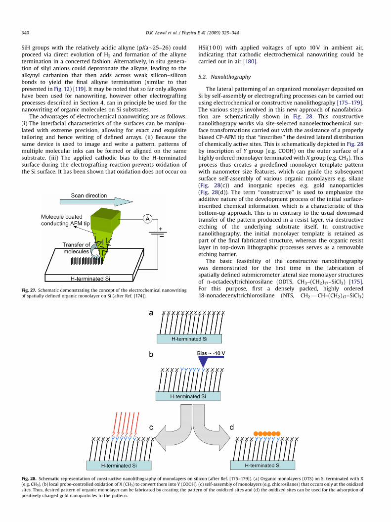
scan, the results are shown in Fig. 24. It is evident that the OTSmonolayer gets grafted in the form of islands and the coverageincreases with increasing the number of scans. Almost fullcoverage is obtained after scan 30, confirming the results obtainedfrom the CV data. The average height of the islands, measuredfrom the line-height profile of AFM images of a partially coveredmonolayer, was found to be �1.3 nm. This height is nearly equal tothe thickness (�1.32 nm) of a fully covered monolayer (asmeasured by ellipsometry) and is close to the theoretical lengthof the OTS molecule (i.e., 1.36 nm). After scan 30, the averageroughness of the sample is o0.5 nm, which supports theelectrochemical grafting of OTS monolayer and not that of a
Fig. 24. 1000 nm�1000 nm AFM images and height profiles (across the white lines dra
different number of CV scans: (a) 1, (b) 10, (c) 20 and (d) 30.
multilayer. Thus, the electrografting of monolayer in the presentcase takes place via 2-dimensional nucleation and growth mode.
The electrical properties of Al/OTS/Si(n++) structures arepresented in Fig. 25. Since Si(n++) is heavily doped, Al/OTS/Si(n++) structures can be considered as a metal/dielectric/metalcapacitor. The leakage current through the OTS monolayer, asshown in Fig. 25 is �10–4 A/cm2 at 1 V. This value is slightly lowerthan that of the OTS monolayer deposited on SiO2/Si bysilanization [2], despite the fact that the native oxide layer isabsent in the present case.
Impedance spectroscopy is a powerful tool that can distinguishbetween different contributions to electrical conduction in
wn in the AFM images) of electrochemically grafted OTS on H-terminated Si after

ARTICLE IN PRESS
100
10-2
10-4
10-6
10-8
-1.0 -0.5 0.0 0.5 1.0
J (A
/cm
2 )
V (Volt)
H/si
OTS/Si
Fig. 25. Current–voltage characteristics for Al/H/Si(n++) and Al/OTS/ Si(n++)
structures. (Note a reduction in current density by four orders in magnitude
by OTS monolayer.) The bias was applied on Al electrode, while Si was
grounded [153].
15000
10000
5000
00 10000 20000 30000
Z’ (Ω)
-Z” (
Ω)
1.MHz 0.6kHz
ROX
RML
COX
CML
Fig. 26. Nyquist plot of Al/OTS/ Si(n++) structure recorded in the frequency range
of 600 Hz to 1 MHz with a bias of 1 V. The solid line is a fit to data using a model
equivalent to the RC circuit shown in the inset (see text) [153].
D.K. Aswal et al. / Physica E 41 (2009) 325–344 339
structures such as Al/OTS/Si(n++) [155]. For instance, usingimpedance spectroscopy it is possible to obtain an independentinformation on it, apart from the OTS monolayer a silicon oxideexits at the interface or not. Impedance spectroscopy involvesmeasurement of real (Z0) and imaginary (Z00) parts of impedance asa function of frequency, and in the present case the data forAl/OTS/Si(n++) structure were measured in the frequency range of600 Hz to 1 MHz with 1 V dc bias. The results have been plotted asZ0 vs. Z00, known as the Nyquist plot, in Fig. 26. Frequency is animplicit parameter in this curve, and low frequency correspondsto points at high Z0. The data have been analyzed using theequivalent circuit shown in the inset of Fig. 26, which is assumedto be a series combination of two parallel RC circuits correspond-ing to OTS monolayer (RML, CML) and silicon oxide (Rox, Cox),respectively. The values of various parameters of the equivalentcircuit obtained by fitting experimental data were RML ¼ 3070.1kO, CML ¼ 1.7870.08 nF, Rox ¼ 0.1170.1 kO and Cox ¼ 0.0017.08nF. The physically insignificant values obtained for Rox and Cox
confirm that silicon oxide is absent at the interface, which is inagreement with XPS measurements. In fact, an improved fitting of
data is obtained when the oxide RC circuit has been removed fromthe equivalent circuit. A capacitance of 7.12�10–7 F/cm2 has beenobtained for the OTS monolayer, indicating a good dielectricbehavior of the electrografted OTS monolayer.
5. Electrochemical printing of monolayers
In the previous section, it has been demonstrated that themono- and multilayers of various functional organic moleculescan be grafted on Si substrates using electrochemical processes.However, to develop hybrid devices, it is essential that the graftedmonolayers should be patterned in spatially defined features witha control down to the nanoscale so that molecular devices canbe integrated with existing electronic structures. The issue ofintegration has been addressed in literature and various methodsto pattern monolayers on the nanoscale, such as, nanoshavingand nanografting [156–159], dip pen nanolithography (DPN)[160–166], soft lithography [167–171], photolithography [172,173] and electrochemical printing and lithography [174–179],have been invented. Here, we briefly review the efforts made onelectrochemical nanowriting, nanolithography and microlithogra-phy of organic monolayers.
5.1. Nanowriting
Electrochemical nanowriting is very similar to the DPN. DPN isa scanning probe nanopatterning technique in which an AFM tip isused to deliver molecules to a surface via a solvent meniscus,which naturally forms in the ambient atmosphere [160–166]. Thisdirect-write technique offers high-resolution patterning capabil-ities for a number of molecular and biomolecular ‘inks’ on avariety of substrates, such as metals, semiconductors andmonolayer functionalized surfaces. In order to create stablenanostructures, it is beneficial to use molecules that self-assembleto the substrate via chemisorption or electrostatic interactions.For example, when alkanethiols are patterned on a gold substrate,a monolayer is formed in which the thiol headgroups formrelatively strong bonds to the gold and the alkane chains extendroughly perpendicular to the surface. Creating nanostructuresusing DPN is a single-step process and does not require the use ofresists. Using DPN it is possible to achieve ultra-high resolutionfeatures with line-widths as small as 10–15 nm with a spatialresolution of 5 nm.
The concept of the electrochemical nanowriting is shown inFig. 27. Here, under an applied potential, molecules can be directlyinterfaced with silicon through a covalent bond [174]. It has beendemonstrated that alkyne electrografting reaction is mediated onthe nanoscale by a CP-AFM. The alkyne molecules are loaded tothe Pt-coated AFM tip by dipping it into liquid alkyne spread onthe native oxide surface of Si (10 0) wafer. The Pt-coated AFM tipis biased (+) and the H-terminated Si surface is biased (�) to drivethe cathodic electrografting reaction under ambient conditions. Asthe tip moves across the Si surface, lines of the electrograftedalkyne are drawn. Lines of monolayer having widths of 40 nmwere produced reproducibly by this method [174]. The height ofthe drawn monolayer, as expected, was found to be nearly equal tothe molecule length. The close proximity of the tip to the siliconsurfaces enables the reaction to proceed in absence of electrolyte.In addition, application of a forward bias during the reactionrenders the surface less sensitive to oxidation. The resultingpatterned monolayers were very stable in air and basic aqueoussolution. The proposed mechanisms of electrochemical nanow-riting are as follows. The application of a negative bias to thesilicon surface is expected to render the SiH groups more hydridicor progress further to silyl anions. Reaction of the forward-biased
ARTICLE IN PRESS
D.K. Aswal et al. / Physica E 41 (2009) 325–344340
SiH groups with the relatively acidic alkyne (pKa�25–26) couldproceed via direct evolution of H2 and formation of the alkynetermination in a concerted fashion. Alternatively, in situ genera-tion of silyl anions could deprotonate the alkyne, leading to thealkynyl carbanion that then adds across weak silicon–siliconbonds to yield the final alkyne termination (similar to thatpresented in Fig. 12) [119]. It may be noted that so far only alkyneshave been used for nanowriting, however other electrograftingprocesses described in Section 4, can in principle be used for thenanowriting of organic molecules on Si substrates.
The advantages of electrochemical nanowriting are as follows.(i) The interfacial characteristics of the surfaces can be manipu-lated with extreme precision, allowing for exact and exquisitetailoring and hence writing of defined arrays. (ii) Because thesame device is used to image and write a pattern, patterns ofmultiple molecular inks can be formed or aligned on the samesubstrate. (iii) The applied cathodic bias to the H-terminatedsurface during the electrografting reaction prevents oxidation ofthe Si surface. It has been shown that oxidation does not occur on
Fig. 28. Schematic representation of constructive nanolithography of monolayers on si
(e.g. CH3), (b) local probe-controlled oxidation of X (CH3) to convert them into Y (COOH),
sites. Thus, desired pattern of organic monolayer can be fabricated by creating the patte
positively charged gold nanoparticles to the pattern.
Fig. 27. Schematic demonstrating the concept of the electrochemical nanowriting
of spatially defined organic monolayer on Si (after Ref. [174]).
HSi(10 0) with applied voltages of upto 10 V in ambient air,indicating that cathodic electrochemical nanowriting could becarried out in air [180].
5.2. Nanolithography
The lateral patterning of an organized monolayer deposited onSi by self-assembly or electrografting processes can be carried outusing electrochemical or constructive nanolithography [175–179].The various steps involved in this new approach of nanofabrica-tion are schematically shown in Fig. 28. This constructivenanolithograpy works via site-selected nanoelectrochemical sur-face transformations carried out with the assistance of a properlybiased CP-AFM tip that ‘‘inscribes’’ the desired lateral distributionof chemically active sites. This is schematically depicted in Fig. 28by inscription of Y group (e.g. COOH) on the outer surface of ahighly ordered monolayer terminated with X group (e.g. CH3). Thisprocess thus creates a predefined monolayer template patternwith nanometer size features, which can guide the subsequentsurface self-assembly of various organic monolayers e.g. silane(Fig. 28(c)) and inorganic species e.g. gold nanoparticles(Fig. 28(d)). The term ‘‘constructive’’ is used to emphasize theadditive nature of the development process of the initial surface-inscribed chemical information, which is a characteristic of thisbottom-up approach. This is in contrary to the usual downwardtransfer of the pattern produced in a resist layer, via destructiveetching of the underlying substrate itself. In constructivenanolithography, the initial monolayer template is retained aspart of the final fabricated structure, whereas the organic resistlayer in top-down lithographic processes serves as a removableetching barrier.
The basic feasibility of the constructive nanolithographywas demonstrated for the first time in the fabrication ofspatially defined submicrometer lateral size monolayer structuresof n-octadecyltrichlorosilane (ODTS, CH3–(CH2)17–SiCl3) [175].For this purpose, first a densely packed, highly ordered18-nonadecenyltrichlorosilane (NTS, CH2QCH–(CH2)17–SiCl3)
licon (after Ref. [175–179]). (a) Organic monolayers (OTS) on Si terminated with X
(c) self-assembly of monolayers (e.g. chlorosilanes) that occurs only at the oxidized
rn of the oxidized sites and (d) the oxidized sites can be used for the adsorption of
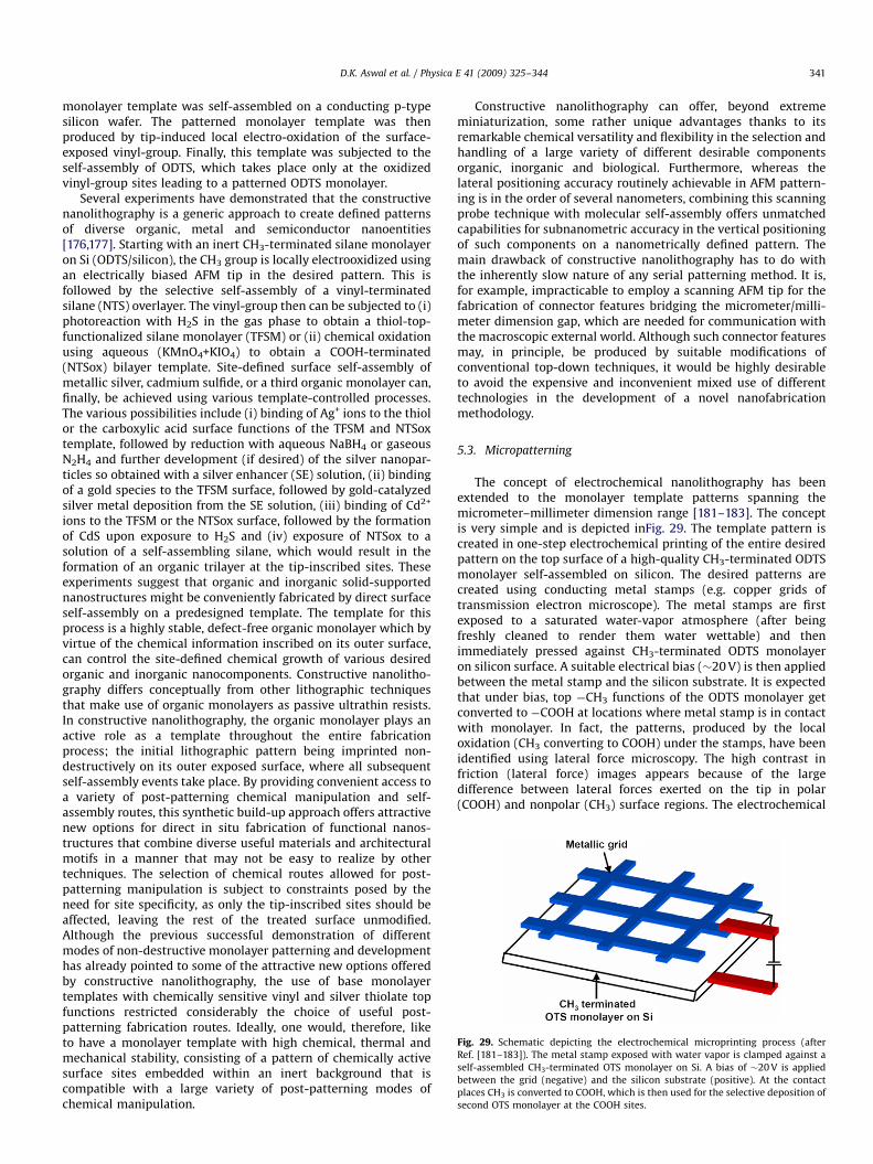
ARTICLE IN PRESS
Fig. 29. Schematic depicting the electrochemical microprinting process (after
Ref. [181–183]). The metal stamp exposed with water vapor is clamped against a
self-assembled CH3-terminated OTS monolayer on Si. A bias of �20 V is applied
between the grid (negative) and the silicon substrate (positive). At the contact
places CH3 is converted to COOH, which is then used for the selective deposition of
second OTS monolayer at the COOH sites.
D.K. Aswal et al. / Physica E 41 (2009) 325–344 341
monolayer template was self-assembled on a conducting p-typesilicon wafer. The patterned monolayer template was thenproduced by tip-induced local electro-oxidation of the surface-exposed vinyl-group. Finally, this template was subjected to theself-assembly of ODTS, which takes place only at the oxidizedvinyl-group sites leading to a patterned ODTS monolayer.
Several experiments have demonstrated that the constructivenanolithography is a generic approach to create defined patternsof diverse organic, metal and semiconductor nanoentities[176,177]. Starting with an inert CH3-terminated silane monolayeron Si (ODTS/silicon), the CH3 group is locally electrooxidized usingan electrically biased AFM tip in the desired pattern. This isfollowed by the selective self-assembly of a vinyl-terminatedsilane (NTS) overlayer. The vinyl-group then can be subjected to (i)photoreaction with H2S in the gas phase to obtain a thiol-top-functionalized silane monolayer (TFSM) or (ii) chemical oxidationusing aqueous (KMnO4+KIO4) to obtain a COOH-terminated(NTSox) bilayer template. Site-defined surface self-assembly ofmetallic silver, cadmium sulfide, or a third organic monolayer can,finally, be achieved using various template-controlled processes.The various possibilities include (i) binding of Ag+ ions to the thiolor the carboxylic acid surface functions of the TFSM and NTSoxtemplate, followed by reduction with aqueous NaBH4 or gaseousN2H4 and further development (if desired) of the silver nanopar-ticles so obtained with a silver enhancer (SE) solution, (ii) bindingof a gold species to the TFSM surface, followed by gold-catalyzedsilver metal deposition from the SE solution, (iii) binding of Cd2+
ions to the TFSM or the NTSox surface, followed by the formationof CdS upon exposure to H2S and (iv) exposure of NTSox to asolution of a self-assembling silane, which would result in theformation of an organic trilayer at the tip-inscribed sites. Theseexperiments suggest that organic and inorganic solid-supportednanostructures might be conveniently fabricated by direct surfaceself-assembly on a predesigned template. The template for thisprocess is a highly stable, defect-free organic monolayer which byvirtue of the chemical information inscribed on its outer surface,can control the site-defined chemical growth of various desiredorganic and inorganic nanocomponents. Constructive nanolitho-graphy differs conceptually from other lithographic techniquesthat make use of organic monolayers as passive ultrathin resists.In constructive nanolithography, the organic monolayer plays anactive role as a template throughout the entire fabricationprocess; the initial lithographic pattern being imprinted non-destructively on its outer exposed surface, where all subsequentself-assembly events take place. By providing convenient access toa variety of post-patterning chemical manipulation and self-assembly routes, this synthetic build-up approach offers attractivenew options for direct in situ fabrication of functional nanos-tructures that combine diverse useful materials and architecturalmotifs in a manner that may not be easy to realize by othertechniques. The selection of chemical routes allowed for post-patterning manipulation is subject to constraints posed by theneed for site specificity, as only the tip-inscribed sites should beaffected, leaving the rest of the treated surface unmodified.Although the previous successful demonstration of differentmodes of non-destructive monolayer patterning and developmenthas already pointed to some of the attractive new options offeredby constructive nanolithography, the use of base monolayertemplates with chemically sensitive vinyl and silver thiolate topfunctions restricted considerably the choice of useful post-patterning fabrication routes. Ideally, one would, therefore, liketo have a monolayer template with high chemical, thermal andmechanical stability, consisting of a pattern of chemically activesurface sites embedded within an inert background that iscompatible with a large variety of post-patterning modes ofchemical manipulation.
Constructive nanolithography can offer, beyond extrememiniaturization, some rather unique advantages thanks to itsremarkable chemical versatility and flexibility in the selection andhandling of a large variety of different desirable componentsorganic, inorganic and biological. Furthermore, whereas thelateral positioning accuracy routinely achievable in AFM pattern-ing is in the order of several nanometers, combining this scanningprobe technique with molecular self-assembly offers unmatchedcapabilities for subnanometric accuracy in the vertical positioningof such components on a nanometrically defined pattern. Themain drawback of constructive nanolithography has to do withthe inherently slow nature of any serial patterning method. It is,for example, impracticable to employ a scanning AFM tip for thefabrication of connector features bridging the micrometer/milli-meter dimension gap, which are needed for communication withthe macroscopic external world. Although such connector featuresmay, in principle, be produced by suitable modifications ofconventional top-down techniques, it would be highly desirableto avoid the expensive and inconvenient mixed use of differenttechnologies in the development of a novel nanofabricationmethodology.
5.3. Micropatterning
The concept of electrochemical nanolithography has beenextended to the monolayer template patterns spanning themicrometer–millimeter dimension range [181–183]. The conceptis very simple and is depicted inFig. 29. The template pattern iscreated in one-step electrochemical printing of the entire desiredpattern on the top surface of a high-quality CH3-terminated ODTSmonolayer self-assembled on silicon. The desired patterns arecreated using conducting metal stamps (e.g. copper grids oftransmission electron microscope). The metal stamps are firstexposed to a saturated water-vapor atmosphere (after beingfreshly cleaned to render them water wettable) and thenimmediately pressed against CH3-terminated ODTS monolayeron silicon surface. A suitable electrical bias (�20 V) is then appliedbetween the metal stamp and the silicon substrate. It is expectedthat under bias, top �CH3 functions of the ODTS monolayer getconverted to �COOH at locations where metal stamp is in contactwith monolayer. In fact, the patterns, produced by the localoxidation (CH3 converting to COOH) under the stamps, have beenidentified using lateral force microscopy. The high contrast infriction (lateral force) images appears because of the largedifference between lateral forces exerted on the tip in polar(COOH) and nonpolar (CH3) surface regions. The electrochemical

ARTICLE IN PRESS
D.K. Aswal et al. / Physica E 41 (2009) 325–344342
oxidation is a non-destructive and therefore does not affect thesurface topography significantly. Upon self-assembly at the sur-face-modified sites of a CH3-terminated NTS monolayer, thehomogeneous nonpolar character of the entire imaged surfacewas restored in the lateral force image. However, in thetopographic image, step corresponding to the expected height ofthe NTS monolayer was clearly observed, indicating that the NTSmonolayer self-assembles only at COOH sites.
It may be noted that experiments performed without exposureof the metal stamps to a saturated water-vapor atmosphere priorto contacting the monolayer surface, no definite patterns could beobserved. This indicates that water layer also plays important rolein the conversion of �CH3 into �COOH. In order to achieve large-area molecular-scale contact between stamp and substrate it isessential that the stamp is made of a flexible soft material, like theelastomeric stamps currently employed in the many versions ofsoft lithography.
6. Summary
We have presented a brief overview of organic moleculesexhibiting various electronic functionalities, such as, dielectric,diode, memory and transistor. We have also discussed variousissues, such as, importance of molecule/Si interface, newmolecular architectures for hybrid devices, etc. It has beendemonstrated that functional organic molecules can be depositedon Si by the cathodic electrochemical process using terminal vinyl(CQC), ethynyl (CRC), halide (Cl, Br, I), tetraalkylammoniumsalt, diazonium salt and silane as reactant. However, in somecases, particularly using diazonium salts, electrografting does notallow easy formation of monolayers, as the formation ofreticulated multilayers is difficult to prevent. The electronicfunctionalities of some electrografted molecules, such as, di-electric behavior in OTS monolayers and resistive memory effectin TPP-C11 monolayers, have been demonstrated. A distinctadvantage of cathodic electrografting over self-assembly is thatthe applied bias not only acts as a control to graft molecules on Sisurface but also circumvents the oxidation of the Si surface duringdeposition. It has also been shown that electrochemistry providesvery useful information on the characteristics of the graftedlayers. An overview of the recent advances made in the spatialpatterning of monolayer using electrochemical lithography ispresented. It has been shown that the electrografting processallows fabrication of monolayer patterns with spatial resolution ina wide range i.e. from nanometer to millimeter. Summing up, thecathodic electrochemical process is a prospective method forgrafting organic molecules to H-terminated Si surfaces andgenerating monolayer patterns with spatial resolution down tonanometer scale for hybrid nanoelectronics.
Acknowledgements
This work is supported by the DAE (India)–CEA (France)collaborative program. We thank Pascal Boulanger for his support.
References
[1] International Technology Roadmap for Semiconductors (IRTS), 2007 /http://www.itrs.net/reports.htmlS.
[2] D.K. Aswal, S. Lenfant, D. Guerin, J.V. Yakhmi, D. Vuillaume, Anal. Chim. Acta568 (2006) 84.
[3] D. Vuillaume, C. R. Phys. 9 (2008) 78.[4] B. Mann, H. Kuhn, J. Appl. Phys. 42 (1971) 4398.[5] A. Aviram, M.A. Ratner, Chem. Phys. Lett. 29 (1974) 277.[6] R.M. Metzger, Chem. Rev. 103 (2003) 3803.[7] D. Vuillaume, J. Nanosci. Nanotechnol. 2 (2002) 267.
[8] M.A. Reed, C. Zhou, C.J. Miller, T.P. Burgin, J.M. Tour, Science 278 (1997) 252.[9] H.B. Weber, J. Reichert, F. Weigend, R. Ochs, D. Beckmann, M. Mayor,
R. Ahlrichs, H. von Lohneysen, Chem. Phys. 281 (2002) 113.[10] C. Kergueris, I.P. Bourgoin, S. Palacin, D. Esteve, C. Urbina, M. Magoga,
C. Joachim, Phys. Rev. B 59 (1999) 12505.[11] J.G. Kushmenck, D.B. Holt, J.C. Yang, J. Naciri, M.H. Moore, R. Shashidhar,
Phys. Rev. Lett. 89 (2002) 086802.[12] A. Bezryadin, C. Dekker, G. Schmid, Appl. Phys. Lett. 71 (1997) 1273.[13] B. Xu, N.J. Tao, Science 301 (2003) 1221.[14] D.J. Wold, C.D. Frisbie, J. Am. Chem. Soc. 123 (2001) 5549.[15] X.D. Cui, X. Zarate, J. Tomfohr, O.F. Sankey, A. Primak, A.L. Moore, T.A. Moore,
D. Gust, G. Harris, S.M. Lindsay, Nanotechnology 13 (2002) 5.[16] J. Chen, M.A. Reed, A.M. Rawlett, J.M. Tour, Science 286 (1999) 1550.[17] C. Zhou, M.R. Deshpande, M.A. Reed, L. Jones II, J.M. Tour, Appl. Phys. Lett. 71
(1997) 611.[18] K.S. Ralls, R.A. Buhrman, R.C. Tiberio, Appl. Phys. Lett. 55 (1989) 2459.[19] A. Salomon, D. Cahen, S.M. Lindsay, J. Tomfohr, V.B. Engelkes, C.D. Frisbie,
Adv. Mater. 15 (2003) 1881.[20] C. Joachim, J.K. Gimzewski, A. Aviram, Nature 408 (2000) 541.[21] G.F. Cerofolini, E. Romano, Appl. Phys. A 91 (2008) 181.[22] J.M. Buriak, Chem. Rev. 102 (2002) 1271.[23] S.F. Bent, Surf. Sci. 500 (2002) 879.[24] G. Cleland, B.R. Horrocks, A. Houlton, J. Chem. Soc. Faraday Trans. 91 (1995)
4001.[25] W.C. Bigelow, D.I. Pickett, W.A. Zisman, J. Colloid Sci. 1 (1946) 513.[26] R. Maoz, J. Sagiv, J. Colloid Interface Sci. 100 (1984) 465.[27] J.B. Brzoska, I.B. Azouz, F. Rondelez, Langmuir 10 (1994) 4367.[28] S.R. Wasserman, Y.-T. Tao, G.M. Whitesides, Langmuir 5 (1989) 1074.[29] N. Tillman, A. Ulman, J.S. Schildkraut, T.L. Penner, J. Am. Chem. Soc. 110
(1988) 6136.[30] M.R. Linford, C.E.D. Chidsey, J. Am. Chem. Soc. 115 (1993) 12631.[31] M.R. Linford, P. Fenter, P.M. Eisenberger, C.E.D. Chidsey, J. Am. Chem. Soc. 117
(1995) 3145.[32] M.M. Sung, J. Kluth, O.W. Yauw, R. Maboudian, Langmuir 13 (1997) 6164.[33] J. Terry, M.R. Linford, C. Wigren, R. Cao, P. Pianetta, C.E.D. Chidsey, Appl. Phys.
Lett. 71 (1997) 1056.[34] R.L. Cicero, M.R. Linford, C.E.D. Chidsey, Langmuir 16 (2000) 5688.[35] M.P. Stewart, F. Maya, D.V. Kosynkin, S.M. Dirk, J.J. Stapleton, C.L. McGuiness,
D.L. Allara, J.M. Tour, J. Am. Chem. Soc. 126 (2004) 370.[36] S. Palacin, C. Bureau, J. Charlier, G. Deniau, B. Mouanda, P. Viel, Chem. Phys.
Chem. 5 (2004) 1468 (and references therein).[37] G. Lecayon, Y. Bouizem, C. Le Gressus, C. Reynaud, C. Boizian, C. Juret, Chem.
Phys. Lett. 91 (1982) 506.[38] G.C. Herdt, A.W. Czanderna, J. Vac. Sci. Technol. A 13 (1995) 1275.[39] D.R. Jung, A.W. Czanderna, Crit. Rev. Solid State Mater. Sci. 191 (1994) 1.[40] D.R. Jung, A.W. Czanderna, G.C. Herdt, J. Vac. Sci. Technol. A 14 (1996) 1779.[41] G.L. Fisher, A.E. Hooper, R.L. Opila, D.L. Allara, N. Winograd, J. Phys. Chem.
B 104 (2000) 3267.[42] G.L. Fisher, A.V. Walker, A.E. Hooper, T.B. Tighe, K.B. Bahnck, H.T. Skriba,
M.D. Reinard, B.C. Haynie, R.L. Opila, N. Winograd, D.L. Allara, J. Am. Chem.Soc. 124 (2002) 5528.
[43] K. Konstadinidis, P. Zhang, R.L. Opila, D.L. Allara, Surf. Sci. 338 (1995) 300.[44] D.K. Aswal, S. Lenfant, D. Guerin, J.V. Yakhmi, D. Vuillaume, Small 1 (2005)
725.[45] D.K. Aswal, C. Petit, G. Salace, D. Guerin, S. Lenfant, J.V. Yakhmi, D. Vuillaume,
Phys. Status Solidi (a) 203 (2006) 1464.[46] J.G. Simmons, J. Appl. Phys. 34 (1963) 2581.[47] E.E. Polymeropoulos, J. Appl. Phys. 48 (1977) 2404.[48] E.E. Polymeropoulos, J. Sagiv, J. Chem. Phys. 69 (1978) 1836.[49] D.J. Wold, C.D. Frisbie, J. Am. Chem. Soc. 122 (2000) 2970.[50] D.J. Wold, C.D. Frisbie, J. Am. Chem. Soc. 123 (2001) 5549.[51] C. Boulas, J.V. Davidovits, F. Rondelez, D. Vuillaume, Phys. Rev. Lett. 76 (1996)
4797.[52] D. Vuillaume, C. Boulas, J. Collet, G. Allan, C. Delerue, Phys. Rev. B 58 (1998)
16491.[53] D.K. Aswal, S. Lenfant, D. Guerin, D. Vuillaume, J.V. Yakhmi, Nanotechnology
16 (2005) 3064.[54] Z. Huang, B. Xu, Y. Chen, M. Di Ventra, N.J. Tao, Nano. Lett. 6 (2006)
1240.[55] N. Clement, S. Pleutin, O. Seitz, S. Lenfant, D. Vuillaume, Phys. Rev. B 76
(2007) 205407.[56] J.R. Petta, S.K. Slater, D.C. Ralph, Phys. Rev. Lett. 93 (2004) 136601.[57] W. Wang, C.A. Richter, Appl. Phys. Lett. 89 (2006) 153105.[58] L.A. Bumm, J.J. Arnold, M.T. Cygan, T.D. Dunbar, T.P. Burgin, L. Jones II,
D.L. Allara, J.M. Tour, P.S. Weiss, Science 271 (1996) 1705.[59] G.J. Ashwell, B. Urasinska, C. Wang, M.R. Bryce, I. Grace, C.J. Lambert, Chem.
Commun. 45 (2006) 4706.[60] L. Patrone, S. Palacin, J. Charlier, F. Armand, J.-P. Bourgoin, H. Tang,
‘S. Gauthier, Phys. Rev. Lett. 91 (2003) 096802.[61] D.S. Seferos, S.A. Trammell, G.C. Bazan, J.G. Kushmerick, PNAS 102 (2005)
8821.[62] F. Paul, C. Lapinte, Coord. Chem. Rev. 178–180 (1998) 431.[63] J. Reimers, T.X. Lu, M.J. Crossley, S. Hush, Nanotechnology 7 (1996) 424.[64] A. Nitzan, M.A. Ratner, Science 300 (2003) 1384.[65] R.M. Metzger, T. Xu, I.R. Peterson, J. Phys. Chem. B 105 (2001) 7280.[66] A.S. Martin, J.R. Sambles, G.J. Ashwell, Phys. Rev. Lett. 70 (1993) 218.

ARTICLE IN PRESS
D.K. Aswal et al. / Physica E 41 (2009) 325–344 343
[67] G.J. Ashwell, J.R. Sambles, A.S. Martin, W.G. Parker, M. Szablewski, J. Chem.Soc. Chem. Commun. 19 (1990) 1374.
[68] R.M. Metzger, B. Chen, U. Hopfner, M.V. Lakshmikantham, D. Vuillaume, T.Kawai, X. Wu, H. Tachibana, T.V. Hughes, H. Sakurai, J.W. Baldwin, C. Hosch,M.P. Cava, L. Brehmer, G.J. Ashwell, J. Am. Chem. Soc. 119 (1997) 10455.
[69] D. Vuillaume, B. Chen, R.M. Metzger, Langmuir 15 (1999) 4011.[70] T. Xu, I.R. Peterson, M.V. Lakshmikantham, R.M. Metzger, Angew. Chem. Int.
Ed. Engl. 40 (2001) 1749.[71] C. Krzeminski, G. Allan, C. Delerue, D. Vuillaume, R.M. Metzger, Phys. Rev. B
64 (2001) 085405.[72] K. Stokbro, J. Taylor, M. Brandbyge, J. Am. Chem. Soc. 125 (2003) 3674.[73] P.E. Kornilovitch, A.M. Bratkovsky, R.S. Williams, Phys. Rev. B 66 (2002)
165436.[74] J. Taylor, M. Brandbyge, K. Stokbro, Phys. Rev. Lett. 89 (2002) 138301.[75] S. Datta, W. Tian, S. Hong, R. Reifenberger, J.I. Henderson, C.P. Kubiak, Phys.
Rev. Lett. 79 (1997) 2530.[76] S. Lenfant, C. Krzeminski, C. Delerue, G. Allan, D. Vuillaume, Nano Lett. 3
(2003) 741.[77] C.P. Collier, E.W. Wong, M. Belohradsky, F.M. Raymo, J.F. Stodart, P.J. Kuekes,
R.S. Williams, J.R. Heath, Science 285 (1999) 391.[78] Y. Chen, D.A.A. Ohlberg, X. Li, D.R. Stewart, R.S. Willaims, Appl. Phys. Lett. 82
(2003) 1610.[79] C.P. Collier, G. Mattersteig, E.W. Wong, Y. Luo, K. Baverly, J. Sampaio, F.M.
Raymo, J.F. Stoddart, J.R. Heath, Science 289 (2000) 1172.[80] C.N. Lau, D.R. Stewart, R.S. Willaims, M. Bockrath, Nano Lett. 4 (2004) 569.[81] D.R. Stewart, D.A.A. Ohlberg, P.A. Beck, Y. Chen, R.S. Willaims, Nano Lett. 4
(2004) 133.[82] J. He, B. Chen, A.K. Flatt, J.J. Stephenson, C.D. Doyle, J.M. Tour, Nat. Mater. 5
(2006) 63.[83] Z.J. Donhauser, B.A. Mantooth, K.F. Kelly, L.A. Bumm, J.D. Monnell,
J.J. Stapleton, D.W. Price, A.M. Rawlett, D.L. Allara, J.M. Tour, P.S. Weiss,Science 292 (2001) 2302.
[84] A.M. Rawlett, T.J. Hopson, L.A. Nagahara, R.K. Tsui, G.K. Ramachandran,S.M. Lindsay, Appl. Phys. Lett. 81 (2002) 3043.
[85] M.A. Reed, J. Chen, A.M. Rawlett, D.W. Price, J.M. Tour, Appl. Phys. Lett. 78(2001) 3735.
[86] C.P. Collier, E.W. Wong, M. Belohradsky, F.M. Raymo, J.F. Stodart, P.J. Kuekes,R.S. Williams, J.R. Heath, Science 285 (1999) 391.
[87] J.M. Seminario, A.G. Zacarias, J.M. Tour, J. Am. Chem. Soc. 122 (2000)3015.
[88] G.K. Ramachandran, T.J. Hopson, A.M. Rawlett, L.A. Nagahara, A. Primak,S.M. Lindsay, Science 300 (2003) 1413.
[89] K.M. Roth, J.S. Lindsey, D.F. Bocian, W.G. Kuhr, Langmuir 18 (2002) 4030.[90] Q. Li, G. Mathur, M. Homsi, S. Surthi, V. Misra, V. Malinovskii, K.-H.
Schweikart, L. Yu, J.S. Lindsey, Z. Liu, R.B. Dabke, A.A. Yasseri, D.F. Bocian,W.G. Kuhr, Appl. Phys. Lett. 81 (2002) 1494.
[91] K.M. Roth, A.A. Yasseri, Z. Liu, R.B. Dabke, V. Malinovskii, K.-H. Schweikart, L.Yu, H. Tiznado, F. Zaera, J.S. Lindsey, W.G. Kuhr, D.F. Bocian, J. Am. Chem. Soc.125 (2003) 505.
[92] Z. Liu, A.A. Yasseri, J.S. Lindsey, D.F. Bocian, Science 302 (2003) 1543.[93] S.M. Sze, Semiconductor Devices: Physics and Technology, Wiley, New York,
2002.[94] N.P. Guisinger, M.E. Greene, R. Basu, A.S. Baluch, M.C. Hersam, Nano Lett. 4
(2004) 55.[95] T. Rakshit, G.-C. Liang, A.W. Ghosh, S. Datta, Nano Lett. 4 (2004) 1803.[96] J.L. Pitters, R.A. Wolkow, Nano Lett. 6 (2006) 390.[97] S.Y. Quek, J.B. Neaton, M.S. Hybertsen, E. Kaxiras, S.G. Louie, Phys. Rev. Lett.
98 (2007) 066807.[98] C.R. Kagan, A. Afzali, R. Martel, L.M. Gignac, P.M. Solomon, A.G. Schrott, B. Ek,
Nano Lett. 3 (2003) 119.[99] J. Collet, D. Vuillaume, Appl. Phys. Lett. 73 (1998) 2681.
[100] J. Collet, O. Tharaud, A. Chapoton, D. Vuillaume, Appl. Phys. Lett. 76 (2000)1941.
[101] G.S. Tulevski, Q. Miao, M. Fukuto, R. Abram, B. Ocko, R. Pindak, M.L.Steigerwald, C.R. Kagan, C. Nuckolls, J. Am. Chem. Soc. 126 (2004) 15048.
[102] D.F. Perepichka, M.R. Bryce, Angew. Chem. Int. Ed. 44 (2005) 5370.[103] Y.J. Chabal, G.S. Higashi, K. Raghavachari, V.A. Burrows, J. Vac. Sci. Technol.
A 7 (1989) 2104.[104] G.S. Hieashi, Y.J. Chabal, G.W. Trucks, K. Raahavachari, Appl. Phys. Lett. 56
(1990) 656.[105] G.S. Higashi, Y.J. Chabal, G.W. Trucks, K. Raghavachari, Appl. Phys. Lett. 56
(1990) 656.[106] G.S. Higashi, R.S. Becker, Y.J. Chabal, A.J. Becker, Appl. Phys. Lett. 58 (1991)
1656.[107] A.G. Cullis, L.D. Canham, P.D.J. Calcott, J. Appl. Phys. 82 (1997) 909.[108] K. Arima, K. Endo, T. Kataoka, Y. Oshikane, H. Inoue, Y. Mori, Appl. Phys. Lett.
76 (2000) 463.[109] D.D.M. Wayner, R.A. Wolkow, J. Chem. Soc. Perkin Trans. 2 (2002) 23.[110] C.M.A. Brett, A.M.O. Brett, Electrochemistry: Principles, methods and
applications, Oxford University Press, Oxford, Great Britain, 1994.[111] V.S. Bagolsky, Fundamentals of Electrochemistry, Wiley Interscience,
New Jersey, 2006.[112] S.P. Koiry, D.K. Aswal, A.K. Chauhan, V. Saxena, S.K. Nayak, S.K. Gupta,
J.V. Yakhmi, Chem. Phys. Lett. 453 (2008) 68.[113] Z. Guo, F. Du, D. Ren, Y. Chen, J. Zheng, Z. Liu, J. Tian, J. Mater. Chem. 16 (2006)
3021.
[114] K.M. Roth, A.A. Yasseri, Z. Liu, R.B. Dabke, V. Malinovskii, K.H. Schweikart,L. Yu, H. Tiznado, F. Zaera, J.S. Lindsey, W.G. Kuhr, D.F. Bocian, J. Am. Chem.Soc. 125 (2003) 505.
[115] X. Qian, A. Tai, X. Sun, S. Xiao, H. Wu, Z. Lu, Y. Wei, Thin Solid Films 285(1996) 433.
[116] S. Gabriel, A.-S. Duwez, R. Jerome, C. Jerome, Langmuir 23 (2007) 159.[117] E.G. Robins, M.P. Stewart, J.M. Buriak, J. Chem. Soc. Chem Commun. (1999)
2479.[118] J.H. Song, M.J. Sailor, J. Am. Chem. Soc. 120 (1998) 2376.[119] J.H. Song, M.J. Sailor, Inorg. Chem. 38 (1999) 1498.[120] N.Y. Kim, P.E. Laibinis, J. Am. Chem. Soc. 120 (1998) 4516.[121] C. Gurtner, A.W. Wun, M.J. Sailor, Angew. Chem. Int. Ed. 38 (1999) 1966.[122] Z.R. Scheibal, W. Xu, J.F. Audiffred, J.E. Henry, J.C. Flakea, Electrochem. Solid-
State Lett. 11 (2008) K81.[123] F. Cattaruzza, A. Cricenti, A. Flamini, M. Girasole, G. Longo, A. Mezzi,
T. Prosperi, J. Mater. Chem. 14 (2004) 1461.[124] F. Cattaruzza, A. Cricenti, A. Flamini, M. Girasole, G. Longo, T. Prosperi,
G. Andreano, L. Cellai, E. Chirivino, Nucleic Acids Res. 34 (2006) e32/1.[125] A. Teyssot, A. Fidelis, S. Fellah, F. Ozanam, J. -N. Chazalviel, Electrochim. Acta
47 (2002) 2565.[126] C. Gurtner, A.W. Wun, M.J. Sailor, Angew. Chem. Int. Ed. 38 (1999) 1966.[127] T. Dubois, F. Ozanam, J.-N. Chazalviel, Electrochem. Soc. Proc. 97 (1997) 296.[128] A. Aurora, F. Cattaruzza, C. Coluzza, V. Della, C. Volpe, G. Di Santo, A. Flamini,
C. Mangano, S. Morpurgo, P. Pallavicini, R. Zanoni, Chemistry— Eur. J. 13(2007) 1240.
[129] D. Wang, J.M. Buriak, Surf. Sci. 590 (2005) 154.[130] F. Anariba, S.H. DuVall, R.L. McCreery, Anal. Chem. 75 (2003) 3837.[131] C. Henry de Villeneuve, J. Pinson, M.-C. Bernard, P. Allongue, J. Phys. Chem. B
101 (1997) 2415–2420.[132] P. Allongue, C. Henry de Villeneuve, J. Pinson, F. Ozanam, J.N. Chazalviel,
X. Wallart, Electrochim. Acta 43 (1998) 2791.[133] P. Allongue, C. Henry de Villeneuve, G. Cherouvrier, R. Cortes, M.-C. Bernard,
J. Electroanal. Chem. 550–551 (2003) 161.[134] P. Allongue, M. Delamar, B. Desbat, O. Fagebaume, R. Hitmi, J. Pinson,
J.-M. Saveant, J. Am. Chem. Soc. 119 (1997) 201.[135] J. Pinson, F. Podvorica, Chem. Soc. Rev. 34 (2005) 429.[136] M. Delamar, G. Desarmot, O. Fagebaume, R. Hitmi, J. Pinson, J.-M. Saveant,
Carbon 35 (1997) 801.[137] J.K. Kariuki, M.T. McDermott, Langmuir 17 (2001) 5947.[138] Y.-C. Liu, R.L. McCreery, J. Am. Chem. Soc. 112 (1995) 11254.[139] F. Anariba, S.H. DuVall, R.L. McCreery, Anal. Chem. 75 (2003) 3837.[140] C. Combellas, F. Kanoufi, D. Mazouzi, A. Thiebault, P. Bertrand, N. Medard,
Polymer 44 (2003) 19.[141] C.A. Dyke, J.M. Tour, Nano Lett. 3 (2003) 1215.[142] J. Wang, M.A. Firestone, O. Auciello, J.A. Carlisle, Langmuir 20 (2004)
11450.[143] M.P. Stewart, F. Maya, D.V. Konsynkin, S.M. Dirk, J.J. Stapelton,
C.L. McGuiness, D.L. Allara, J.M. Tour, J. Am. Chem. Soc. 126 (2004) 370.[144] A. Adenier, M.-C. Bernard, M.M. Chehimi, E. Cabet-Deliry, B. Desbat,
O. Fagebaume, J. Pinson, F. Podvorica, J. Am. Chem. Soc. 123 (2001) 4541.[145] M.-C. Bernard, A. Chausse, E. Cabet-Deliry, M.M. Chehimi, J. Pinson,
F. Podvorica, C. Vautrin-Ul, Chem. Mater. 15 (2003) 3450.[146] B.L. Hurley, R.L. McCreery, J. Electrochem. Soc. 151 (2004) B252.[147] C. Combellas, F. Kanoufi, J. Pinson, F. Podvorica, Langmuir 21 (2005)
280–286.[148] T. Itoh, R.L. McCreery, J. Am. Chem. Soc. 124 (2002) 10894.[149] C. Combellas, F. Kanoufi, J. Pinson, F. Podvorica, J. Am. Chem.Soc. 130 (2008)
8576.[150] J. Charlier, S. Palacin, J. Leroy, F. Del Frari, L. Zagonel, N. Barrett, O. Renault,
A. Bailly, D. Mariolle, Denis J. Mater. Chem. 18 (2008) 3136.[151] J. Charlier, L. Baraton, C. Bureau, S. Palacin, Chem. Phys. Chem 6 (2005) 70.[152] S.M. Dirk, S. Pylypenko, S.W. Howell, W. Stephen, J.E. Fulghum, D.R. Wheeler,
Langmuir 21 (2005) 10899.[153] S.P. Koiry, D.K. Aswal, Vibha Saxena, N. Padma, A.K. Chauhan, N. Joshi,
S.K. Gupta, J.V. Yakhmi, D. Guerin, D. Vuillaume, Appl. Phys. Lett. 90 (2007)113118.
[154] D. Briggs, M.P. Seah, Practical Surface Analysis by Auger and X-rayPhotoelectron Spectroscopy, Wiley, New York, 1983.
[155] R. Macdonald, Impedance Spectroscopy: Emphasizing Solid Materials andSystems, Wiley-Interscience, New York, 1987.
[156] S. Xu, G.-Y. Liu, Langmuir 12 (1997) 1127.[157] X.D. Xiao, G.Y. Liu, D.H. Charych, M. Salmeron, Langmuir 11 (1995) 1600.[158] W. Kiridena, V. Jain, P.K. Kuo, G.Y. Liu, Surf. Interface Anal. 25 (1997) 383.[159] G.-Y. Liu, S. Xu, Y. Qian, Acc. Chem. Res. 33 (2000) 457.[160] R.D. Piner, J. Zhu, F. Xu, S.H. Hong, C.A. Mirkin, Science 283 (1999) 661.[161] S. Hong, J. Zhu, C.A. Mirkin, Science 286 (1999) 523.[162] S. Hong, C.A. Mirkin, Science 288 (2000) 1808.[163] A. Ivanisevic, C.A. Mirkin, J. Am. Chem. Soc. 123 (2001) 7887.[164] K. Salaita, Y. Wang, C.A. Mirkin, Nat. Nanotechnol. 2 (2007) 145.[165] H. Zhang, Z. Li, C.A. Mirkin, Adv. Mater. 14 (2002) 1472.[166] S. Rozhok, R. Piner, C.A. Mirkin, J. Phys. Chem. B 107 (2003) 751.[167] Y.N. Xia, G.M. Whitesides, Angew. Chem. Int. Ed. 37 (1998) 551.[168] Y.N. Xia, J.A. Rogers, K.E. Paul, G.M. Whitesides, Chem. Rev. 99 (1999) 1823.[169] T.W. Odom, V.R. Thalladi, C. Love, G.M. Whitesides, J. Am. Chem. Soc. 124
(2002) 12112.[170] W.R. Childs, R.G. Nuzzo, J. Am. Chem. Soc. 124 (2002) 13583.

ARTICLE IN PRESS
D.K. Aswal et al. / Physica E 41 (2009) 325–344344
[171] J.C. Love, D.B. Wolfe, R. Haasch, M.L. Chabinyc, K.E. Paul, G.M. Whitesides,R.G. Nuzzo, J. Am. Chem. Soc. 125 (2003) 2597.
[172] J.T.C. Wojtyk, M. Tomietto, R. Boukherroub, D.D.M. Wayner, . J. Am. Chem.Soc. 123 (2001) 1535.
[173] L.A. Porter, H.C. Choi, J.A. Schmeltzer, J.M. Buriak, Nano Lett. 2 (2002) 1369.[174] P.T. Hurley, A.E. Ribbe, J.M. Buriak, J. Am. Chem. Soc. 125 (2003) 11334.[175] R. Maoz, S.R. Cohen, J. Sagiv, Adv. Mater. 11 (1999) 55.[176] R. Maoz, E. Frydman, S.R. Cohen, J. Sagiv, J. Adv. Mater. 12 (2000) 424.
[177] R. Maoz, E. Frydman, S.R. Cohen, J. Sagiv, J. Adv. Mater. 12 (2000) 725.[178] D. Wouters, U.S. Schubert, Langmuir 19 (2003) 9033.[179] S. Hoeppener, U.S. Schubert, Small 1 (2005) 628.[180] F. Marchi, V. Bouchiat, H. Dallaporta, V. Safarov, D. Tonneau, P. Doppelt,
J. Vac. Sci. Technol. B 16 (1998) 2952.[181] S. Hoeppener, R. Maoz, J. Sagiv, Nano Lett. 3 (2003) 761.[182] S. Liu, R. Maoz, J. Sagiv, Nano Lett. 4 (2004) 845.[183] S. Hoeppener, R. Maoz, J. Sagiv, Adv. Mater. 18 (2006) 1286.