Embed Size (px)
Citation preview

p s sreprints
statu
s
soli
di
www.interscience.wiley.comph
ysi
ca
REPRINT
www.pss-rrl.com
www.pss-c.com
www.pss-b.com
www.pss-a.com
© 2009 WILEY-VCH Verlag GmbH & Co. KGaA, Weinheim
Phys. Status Solidi A 206, No. 2, 256–262 (2009) / DOI 10.1002/pssa.200824290 p s sapplications and materials science
a
statu
s
soli
di
www.pss-a.comph
ysi
ca
In-situ boron doping of chemical-bath deposited CdS thin films
Hani Khallaf1, Guangyu Chai2, Oleg Lupan1, 3, Lee Chow*, 1, 4, 5, Helge Heinrich1, 4, 5, S. Park1, and Alfons Schulte1
1 Department of Physics, University of Central Florida, Orlando, FL 32816, USA 2 Apollo Technologies, Inc., 205 Waymont Court, Suite 111, Lake Mary, FL 32746, USA 3 Department of Microelectronics and Semiconductor Devices, Technical University of Moldova, 168 Stefan cel Mare Boulevard,
2004 Chisinau, Republic of Moldova 4 Advanced Materials Processing and Analysis Center, University of Central Florida, Orlando, FL 32816, USA 5 Department of Mechanical, Materials, Aerospace Engineering, University of Central Florida, Orlando, FL 32816, USA
Received 15 July 2008, revised 25 October 2008, accepted 10 November 2008
Published online 5 January 2009
PACS 61.72.uj, 71.55.Gs, 73.61.Ga, 78.20.Ci, 81.16.Be
* Corresponding author: e-mail [email protected], Phone: +1 407 823 2333, Fax: +1 407 823 5112
© 2009 WILEY-VCH Verlag GmbH & Co. KGaA, Weinheim
1 Introduction Due to its wide bandgap (2.42 eV), photoconductivity, and high electron affinity, CdS has been widely used as a window material in high-efficiency thin-film solar cells based on CdTe and Cu(In,Ga)Se2 [1, 2]. Chemical-bath deposition (CBD) is one of the most commonly used techniques to grow CdS thin films [3, 4]. It is known to be a simple, low-temperature, and inexpen-sive large-area deposition technique for group II–VI semi-conductors such as CdS. CdS films grown by CBD are known to be highly stoichiometric and exhibit a high dark resistance. A dark resistivity as high as 108 Ω cm [5], 109 Ω cm [6], and 1010 Ω cm [7] has been reported earlier for CBD–CdS. In a previous study [3], we have establish- ed a direct relationship between Cd precursors used in the deposition of CBD–CdS and film resistivity. Film resistivity was found to vary from 3.88 × 10³ Ω cm to 8.01 × 101 Ω cm, depending on the Cd precursor used and film stoichiometry. Although a resistivity of 8.01 × 101 Ω cm is low for CBD–CdS, a lower resistivity
is needed for solar cells and other optoelectronic applica- tions. One approach to reduce dark resistivity of CBD–CdS is in-situ doping. Over the past two decades, in-situ doping of CBD–CdS using Al [8–10], Cu [11, 12], Li [13, 14], and Na [15] has been reported. In this work, the effective-ness of B3+ doping through chemical-bath deposition is in-vestigated. Transmittance and reflectance measurements of doped films were carried out to study the effect of B dop-ing on the optical properties and bandgap of CdS films. Resistivity, carrier concentration, and Hall mobility of doped films were acquired using Hall effect measurements. Crystal structure as well as crystal quality and a phase transition were determined using X-ray diffraction (XRD), transmission electron microscopy (TEM), and micro-Raman spectroscopy. Film morphology was studied using scanning electron microscopy (SEM). Film chemistry and binding states were studied using X-ray photoelectron spectroscopy (XPS).
In-situ boron doping of CdS using chemical-bath deposition
(CBD) is reported. The effect of B doping on optical proper-
ties, as well as electrical properties, crystal structure, chemis-
try, and morphology of CdS films is studied. We present a
successful approach towards B doping of CdS using CBD,
where a resistivity as low as 1.7 × 10⁻² Ω cm and a carrier
density as high as 1.91 × 1019 cm–3 were achieved. The band-
gap of B-doped films was found to slightly decrease as the
[B]/[Cd] ratio in the solution increases. X-ray diffraction
studies showed B3+ ions likely enter the lattice substitution-
ally. A phase transition, due to annealing, as well as induced
lattice defects, due to B doping, were detected by micro-
Raman spectroscopy and transmission electron microscopy.
The chemistry and morphology of films were unaffected by B
doping.
Phys. Status Solidi A 206, No. 2 (2009) 257
www.pss-a.com © 2009 WILEY-VCH Verlag GmbH & Co. KGaA, Weinheim
Original
Paper
2 Experimental details CdS films were prepared using stock solutions of CdSO4 (0.038 M), (NH4)2SO4 (0.076 M), NH3OH (29.4%), and (NH2)2CS (0.076 M). Films were grown on 38 mm × 38 mm × 1 mm glass sub-strates (Schott Borofloat glass, supplied by S.I. Howard Glass Co., Inc.). Boron doping was carried out by adding boric acid (H3BO3) as the dopant source to the main solu-tion. The deposition temperature was kept constant at 85 °C. After deposition, all films were annealed at 300 °C in argon ambient for 1 h. Details of the growth process have been previously reported [3]. The cleaning steps of the substrate are reported elsewhere [8]. Alpha-step 500 surface profilometer (Tencor) was used to determine film thickness. Specular transmittance meas-urements were carried out at room temperature with unpo-larized light at normal incidence in the wavelength range from 350 nm to 1200 nm using a Cary 500 (Varian) dou-ble-beam UV/VIS spectrophotometer. Specular reflectance measurements were carried out at an angle of incidence of 7° in the same wavelength range. The optical absorption coefficient α was calculated for each film using the equa-tion [16]:
2(1 ) exp ( ) ,T R tα= - - (1)
where T is transmittance, R is reflectance, and t is film thickness (Table 1). The absorption coefficient α is related to the incident photon energy hν as:
/ 2
g( ),
n
K h E
h
ν
α
ν
-
= (2)
where K is a constant, Eg is the optical bandgap, and n is equal to 1 for direct bandgap materials such as CdS. The bandgap was determined for each film by plotting (αhν)2 versus hν and then extrapolating the straight-line portion to the energy axis. XRD was carried out using a Ri- gaku D XRD unit (with 40 kV, 30 mA Cu Kα radiation, λ = 0.15406 nm). The sample was mounted at 2.5° and scanned from 25–55° in steps of 0.02° with a scan rate of 1.2° min–1. Transmission electron microscopy was per-formed using a Tecnai F30 TEM at an acceleration voltage of 300 kV. Cross sections of the B-doped CdS film were prepared with a FEI 200 focused ion beam system. Resist-ivity, Hall mobility, and carrier density were evaluated by Table 1 Film thickness of B-doped CdS films grown at different [B]/[Cd] ratios (0.0 ratio is assigned to the undoped film).
[B]/[Cd] ratio film thickness (Å)
0.0 1400 8.5 × 10⁻³ 1600 1.7 × 10⁻² 1100 3.4 × 10⁻² 1200 5.1 × 10⁻² 1200 6.8 × 10⁻² 1300 0.1 1300
Hall effect measurements at room temperature in a Van der Pauw four-point probe configuration, using indium con-tacts, in an automated Hall effect system (Ecopia HMS-3000, Bridge Technology, Chandler Heights, AZ, USA) with a 0.55 T magnetic induction. Micro-Raman scattering was performed at room temperature with a Horiba Jobin Yvon LabRam IR system at a spatial resolution of 2 µm in a backscattering configuration. A 632.8 nm line of a he-lium-neon laser was used for off-resonance excitation with less than 4 mW power at the sample. The spectral resolu-tion was 2 cm−1, and the instrument was calibrated to the same accuracy using a naphthalene standard. XPS was per-formed on a Physical Electronics PHI 5400 ESCA using unmonochromated Mg K
α radiation at 1253.6 eV. Each of
the XPS spectra was acquired from 30 repeated sweeps. XPS spectra were corrected from charging effects by refer-encing the adventitious C 1s peak to 284.6 eV. SEM mi-crographs were obtained using JEOL 6400F SEM at an acceleration voltage of 10 kV.
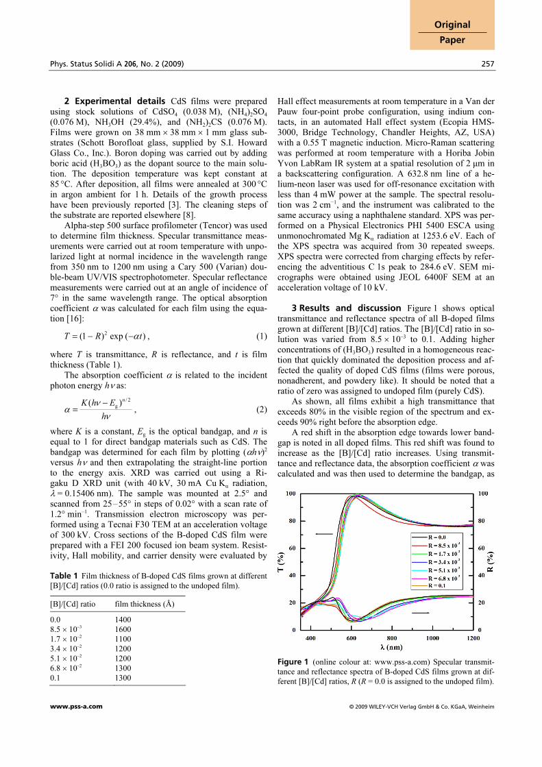
3 Results and discussion Figure 1 shows optical transmittance and reflectance spectra of all B-doped films grown at different [B]/[Cd] ratios. The [B]/[Cd] ratio in so-lution was varied from 8.5 × 10⁻³ to 0.1. Adding higher concentrations of (H3BO3) resulted in a homogeneous reac-tion that quickly dominated the deposition process and af-fected the quality of doped CdS films (films were porous, nonadherent, and powdery like). It should be noted that a ratio of zero was assigned to undoped film (purely CdS). As shown, all films exhibit a high transmittance that exceeds 80% in the visible region of the spectrum and ex-ceeds 90% right before the absorption edge. A red shift in the absorption edge towards lower band-gap is noted in all doped films. This red shift was found to increase as the [B]/[Cd] ratio increases. Using transmit-tance and reflectance data, the absorption coefficient α was calculated and was then used to determine the bandgap, as
Figure 1 (online colour at: www.pss-a.com) Specular transmit-tance and reflectance spectra of B-doped CdS films grown at dif-ferent [B]/[Cd] ratios, R (R = 0.0 is assigned to the undoped film).
258 H. Khallaf et al.: In-situ boron doping of chemical-bath deposited CdS thin films
© 2009 WILEY-VCH Verlag GmbH & Co. KGaA, Weinheim www.pss-a.com
ph
ysic
ap s sstat
us
solid
i a
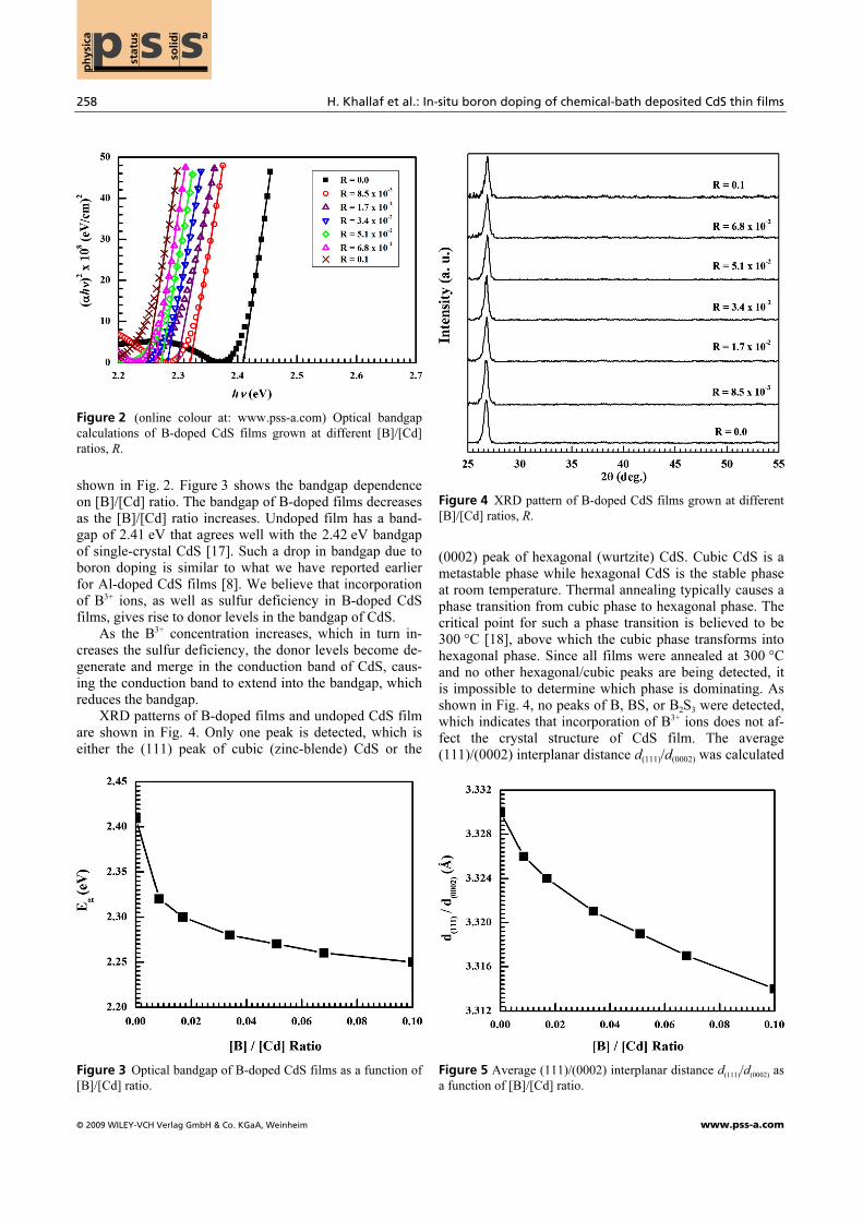
Figure 2 (online colour at: www.pss-a.com) Optical bandgap calculations of B-doped CdS films grown at different [B]/[Cd] ratios, R.
shown in Fig. 2. Figure 3 shows the bandgap dependence on [B]/[Cd] ratio. The bandgap of B-doped films decreases as the [B]/[Cd] ratio increases. Undoped film has a band-gap of 2.41 eV that agrees well with the 2.42 eV bandgap of single-crystal CdS [17]. Such a drop in bandgap due to boron doping is similar to what we have reported earlier for Al-doped CdS films [8]. We believe that incorporation of B3+ ions, as well as sulfur deficiency in B-doped CdS films, gives rise to donor levels in the bandgap of CdS. As the B3+ concentration increases, which in turn in-creases the sulfur deficiency, the donor levels become de-generate and merge in the conduction band of CdS, caus-ing the conduction band to extend into the bandgap, which reduces the bandgap. XRD patterns of B-doped films and undoped CdS film are shown in Fig. 4. Only one peak is detected, which is either the (111) peak of cubic (zinc-blende) CdS or the
Figure 3 Optical bandgap of B-doped CdS films as a function of [B]/[Cd] ratio.
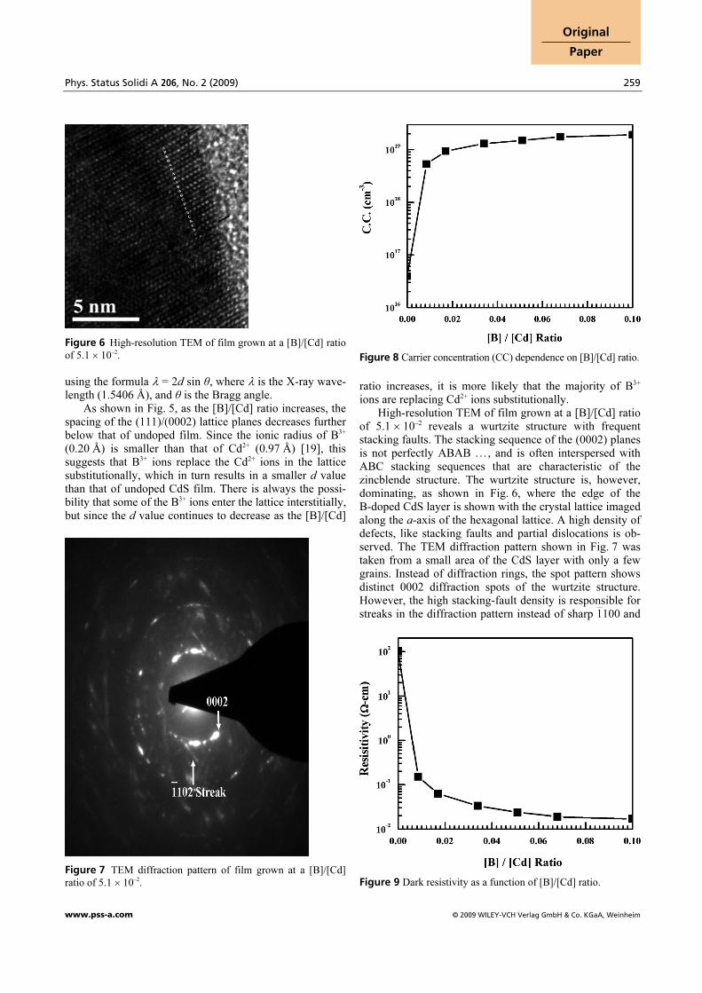
Figure 4 XRD pattern of B-doped CdS films grown at different [B]/[Cd] ratios, R.
(0002) peak of hexagonal (wurtzite) CdS. Cubic CdS is a metastable phase while hexagonal CdS is the stable phase at room temperature. Thermal annealing typically causes a phase transition from cubic phase to hexagonal phase. The critical point for such a phase transition is believed to be 300 °C [18], above which the cubic phase transforms into hexagonal phase. Since all films were annealed at 300 °C and no other hexagonal/cubic peaks are being detected, it is impossible to determine which phase is dominating. As shown in Fig. 4, no peaks of B, BS, or B2S3 were detected, which indicates that incorporation of B3+ ions does not af-fect the crystal structure of CdS film. The average (111)/(0002) interplanar distance d(111)/d(0002) was calculated
Figure 5 Average (111)/(0002) interplanar distance d(111)/d(0002) as a function of [B]/[Cd] ratio.
Phys. Status Solidi A 206, No. 2 (2009) 259
www.pss-a.com © 2009 WILEY-VCH Verlag GmbH & Co. KGaA, Weinheim
Original
Paper
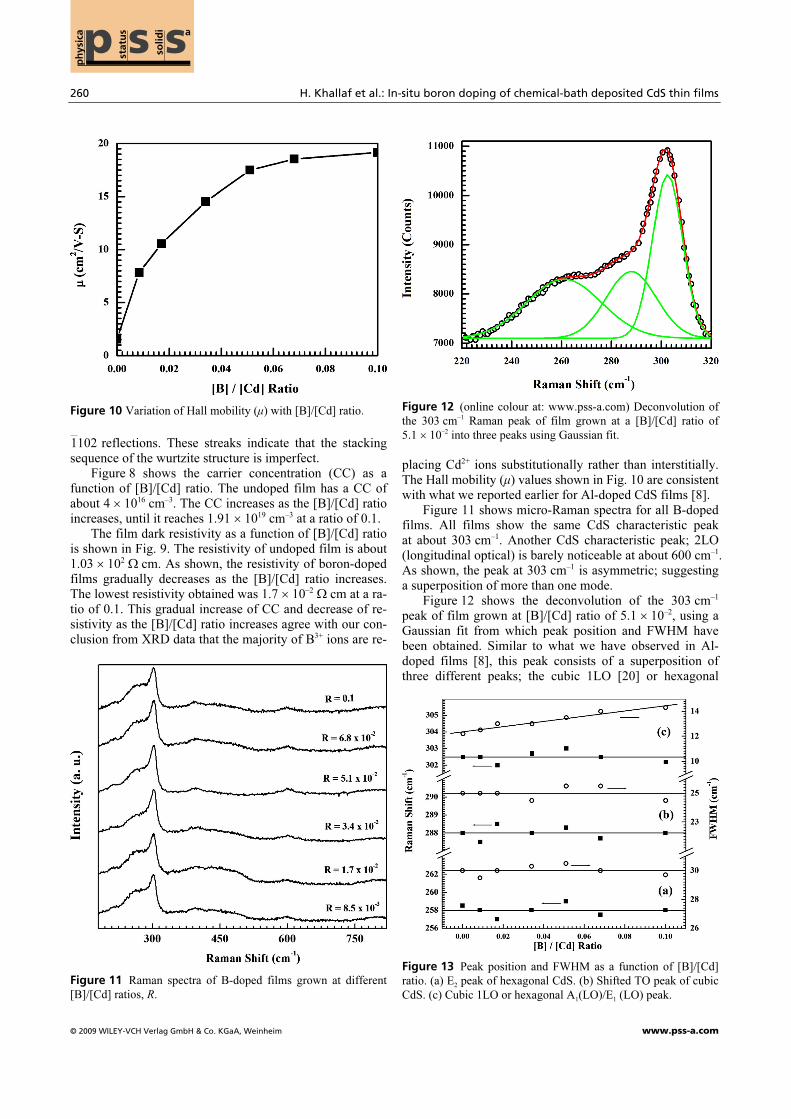
Figure 6 High-resolution TEM of film grown at a [B]/[Cd] ratio of 5.1 × 10⁻². using the formula λ = 2d sin θ, where λ is the X-ray wave-length (1.5406 Å), and θ is the Bragg angle. As shown in Fig. 5, as the [B]/[Cd] ratio increases, the spacing of the (111)/(0002) lattice planes decreases further below that of undoped film. Since the ionic radius of B3+ (0.20 Å) is smaller than that of Cd2+ (0.97 Å) [19], this suggests that B3+ ions replace the Cd2+ ions in the lattice substitutionally, which in turn results in a smaller d value than that of undoped CdS film. There is always the possi-bility that some of the B3+ ions enter the lattice interstitially, but since the d value continues to decrease as the [B]/[Cd]
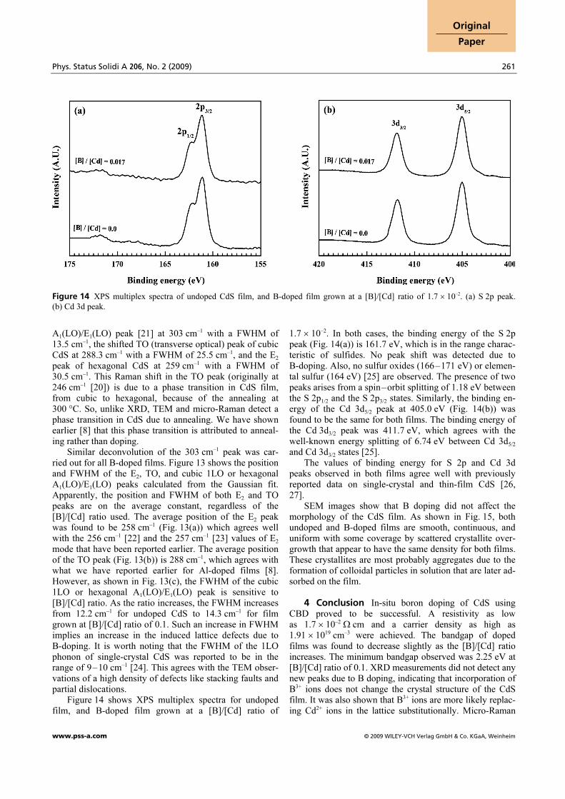
Figure 7 TEM diffraction pattern of film grown at a [B]/[Cd] ratio of 5.1 × 10⁻².
Figure 8 Carrier concentration (CC) dependence on [B]/[Cd] ratio.
ratio increases, it is more likely that the majority of B3+ ions are replacing Cd2+ ions substitutionally. High-resolution TEM of film grown at a [B]/[Cd] ratio of 5.1 × 10⁻² reveals a wurtzite structure with frequent stacking faults. The stacking sequence of the (0002) planes is not perfectly ABAB . . . , and is often interspersed with ABC stacking sequences that are characteristic of the zincblende structure. The wurtzite structure is, however, dominating, as shown in Fig. 6, where the edge of the B-doped CdS layer is shown with the crystal lattice imaged along the a-axis of the hexagonal lattice. A high density of defects, like stacking faults and partial dislocations is ob-served. The TEM diffraction pattern shown in Fig. 7 was taken from a small area of the CdS layer with only a few grains. Instead of diffraction rings, the spot pattern shows distinct 0002 diffraction spots of the wurtzite structure. However, the high stacking-fault density is responsible for streaks in the diffraction pattern instead of sharp 1100 and
Figure 9 Dark resistivity as a function of [B]/[Cd] ratio.
260 H. Khallaf et al.: In-situ boron doping of chemical-bath deposited CdS thin films
© 2009 WILEY-VCH Verlag GmbH & Co. KGaA, Weinheim www.pss-a.com
ph
ysic
ap s sstat
us
solid
i a
Figure 10 Variation of Hall mobility (µ) with [B]/[Cd] ratio.
1102 reflections. These streaks indicate that the stacking sequence of the wurtzite structure is imperfect. Figure 8 shows the carrier concentration (CC) as a function of [B]/[Cd] ratio. The undoped film has a CC of about 4 × 1016 cm–3. The CC increases as the [B]/[Cd] ratio increases, until it reaches 1.91 × 1019 cm–3 at a ratio of 0.1. The film dark resistivity as a function of [B]/[Cd] ratio is shown in Fig. 9. The resistivity of undoped film is about 1.03 × 10² Ω cm. As shown, the resistivity of boron-doped films gradually decreases as the [B]/[Cd] ratio increases. The lowest resistivity obtained was 1.7 × 10⁻² Ω cm at a ra-tio of 0.1. This gradual increase of CC and decrease of re-sistivity as the [B]/[Cd] ratio increases agree with our con-clusion from XRD data that the majority of B3+ ions are re-
Figure 11 Raman spectra of B-doped films grown at different [B]/[Cd] ratios, R.
Figure 12 (online colour at: www.pss-a.com) Deconvolution of the 303 cm–1 Raman peak of film grown at a [B]/[Cd] ratio of 5.1 × 10⁻² into three peaks using Gaussian fit. placing Cd2+ ions substitutionally rather than interstitially. The Hall mobility (μ) values shown in Fig. 10 are consistent with what we reported earlier for Al-doped CdS films [8]. Figure 11 shows micro-Raman spectra for all B-doped films. All films show the same CdS characteristic peak at about 303 cm–1. Another CdS characteristic peak; 2LO (longitudinal optical) is barely noticeable at about 600 cm–1. As shown, the peak at 303 cm–1 is asymmetric; suggesting a superposition of more than one mode. Figure 12 shows the deconvolution of the 303 cm–1 peak of film grown at [B]/[Cd] ratio of 5.1 × 10⁻², using a Gaussian fit from which peak position and FWHM have been obtained. Similar to what we have observed in Al-doped films [8], this peak consists of a superposition of three different peaks; the cubic 1LO [20] or hexagonal
Figure 13 Peak position and FWHM as a function of [B]/[Cd] ratio. (a) E2 peak of hexagonal CdS. (b) Shifted TO peak of cubic CdS. (c) Cubic 1LO or hexagonal A1(LO)/E1 (LO) peak.
Phys. Status Solidi A 206, No. 2 (2009) 261
www.pss-a.com © 2009 WILEY-VCH Verlag GmbH & Co. KGaA, Weinheim
Original
Paper
Figure 14 XPS multiplex spectra of undoped CdS film, and B-doped film grown at a [B]/[Cd] ratio of 1.7 × 10⁻². (a) S 2p peak. (b) Cd 3d peak.
A1(LO)/E1(LO) peak [21] at 303 cm–1 with a FWHM of 13.5 cm–1, the shifted TO (transverse optical) peak of cubic CdS at 288.3 cm–1 with a FWHM of 25.5 cm–1, and the E2 peak of hexagonal CdS at 259 cm–1 with a FWHM of 30.5 cm–1. This Raman shift in the TO peak (originally at 246 cm–1 [20]) is due to a phase transition in CdS film, from cubic to hexagonal, because of the annealing at 300 °C. So, unlike XRD, TEM and micro-Raman detect a phase transition in CdS due to annealing. We have shown earlier [8] that this phase transition is attributed to anneal-ing rather than doping. Similar deconvolution of the 303 cm–1 peak was car-ried out for all B-doped films. Figure 13 shows the position and FWHM of the E2, TO, and cubic 1LO or hexagonal A1(LO)/E1(LO) peaks calculated from the Gaussian fit. Apparently, the position and FWHM of both E2 and TO peaks are on the average constant, regardless of the [B]/[Cd] ratio used. The average position of the E2 peak was found to be 258 cm–1 (Fig. 13(a)) which agrees well with the 256 cm–1 [22] and the 257 cm–1 [23] values of E2 mode that have been reported earlier. The average position of the TO peak (Fig. 13(b)) is 288 cm–1, which agrees with what we have reported earlier for Al-doped films [8]. However, as shown in Fig. 13(c), the FWHM of the cubic 1LO or hexagonal A1(LO)/E1(LO) peak is sensitive to [B]/[Cd] ratio. As the ratio increases, the FWHM increases from 12.2 cm–1 for undoped CdS to 14.3 cm–1 for film grown at [B]/[Cd] ratio of 0.1. Such an increase in FWHM implies an increase in the induced lattice defects due to B-doping. It is worth noting that the FWHM of the 1LO phonon of single-crystal CdS was reported to be in the range of 9–10 cm–1 [24]. This agrees with the TEM obser-vations of a high density of defects like stacking faults and partial dislocations. Figure 14 shows XPS multiplex spectra for undoped film, and B-doped film grown at a [B]/[Cd] ratio of
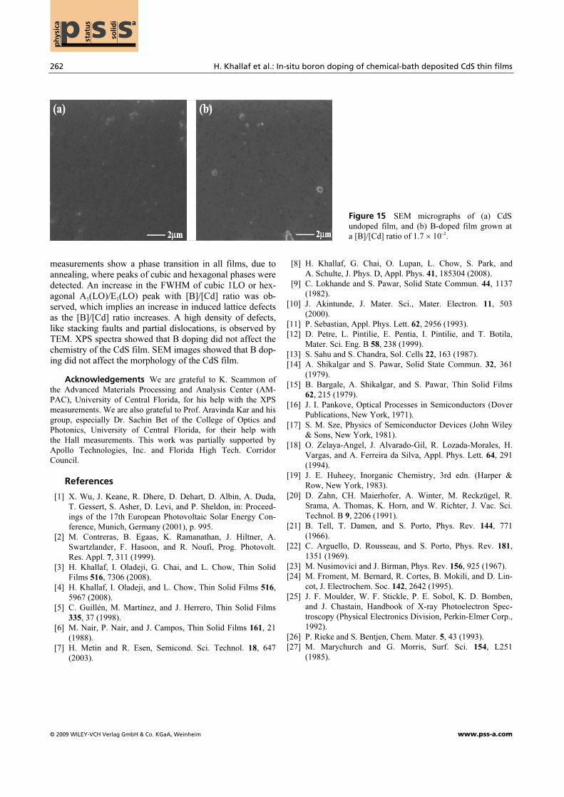
1.7 × 10⁻². In both cases, the binding energy of the S 2p peak (Fig. 14(a)) is 161.7 eV, which is in the range charac-teristic of sulfides. No peak shift was detected due to B-doping. Also, no sulfur oxides (166–171 eV) or elemen-tal sulfur (164 eV) [25] are observed. The presence of two peaks arises from a spin–orbit splitting of 1.18 eV between the S 2p1/2 and the S 2p3/2 states. Similarly, the binding en-ergy of the Cd 3d5/2 peak at 405.0 eV (Fig. 14(b)) was found to be the same for both films. The binding energy of the Cd 3d3/2 peak was 411.7 eV, which agrees with the well-known energy splitting of 6.74 eV between Cd 3d5/2 and Cd 3d3/2 states [25]. The values of binding energy for S 2p and Cd 3d peaks observed in both films agree well with previously reported data on single-crystal and thin-film CdS [26, 27]. SEM images show that B doping did not affect the morphology of the CdS film. As shown in Fig. 15, both undoped and B-doped films are smooth, continuous, and uniform with some coverage by scattered crystallite over-growth that appear to have the same density for both films. These crystallites are most probably aggregates due to the formation of colloidal particles in solution that are later ad-sorbed on the film.
4 Conclusion In-situ boron doping of CdS using CBD proved to be successful. A resistivity as low as 1.7 × 10⁻² Ω cm and a carrier density as high as 1.91 × 1019 cm–3 were achieved. The bandgap of doped films was found to decrease slightly as the [B]/[Cd] ratio increases. The minimum bandgap observed was 2.25 eV at [B]/[Cd] ratio of 0.1. XRD measurements did not detect any new peaks due to B doping, indicating that incorporation of B3+ ions does not change the crystal structure of the CdS film. It was also shown that B3+ ions are more likely replac-ing Cd2+ ions in the lattice substitutionally. Micro-Raman
262 H. Khallaf et al.: In-situ boron doping of chemical-bath deposited CdS thin films
© 2009 WILEY-VCH Verlag GmbH & Co. KGaA, Weinheim www.pss-a.com
ph
ysic
ap s sstat
us
solid
i a
measurements show a phase transition in all films, due to annealing, where peaks of cubic and hexagonal phases were detected. An increase in the FWHM of cubic 1LO or hex-agonal A1(LO)/E1(LO) peak with [B]/[Cd] ratio was ob-served, which implies an increase in induced lattice defects as the [B]/[Cd] ratio increases. A high density of defects, like stacking faults and partial dislocations, is observed by TEM. XPS spectra showed that B doping did not affect the chemistry of the CdS film. SEM images showed that B dop-ing did not affect the morphology of the CdS film.
Acknowledgements We are grateful to K. Scammon of the Advanced Materials Processing and Analysis Center (AM-PAC), University of Central Florida, for his help with the XPS measurements. We are also grateful to Prof. Aravinda Kar and his group, especially Dr. Sachin Bet of the College of Optics and Photonics, University of Central Florida, for their help with the Hall measurements. This work was partially supported by Apollo Technologies, Inc. and Florida High Tech. Corridor Council.
References
[1] X. Wu, J. Keane, R. Dhere, D. Dehart, D. Albin, A. Duda, T. Gessert, S. Asher, D. Levi, and P. Sheldon, in: Proceed-ings of the 17th European Photovoltaic Solar Energy Con-ference, Munich, Germany (2001), p. 995.
[2] M. Contreras, B. Egaas, K. Ramanathan, J. Hiltner, A. Swartzlander, F. Hasoon, and R. Noufi, Prog. Photovolt. Res. Appl. 7, 311 (1999).
[3] H. Khallaf, I. Oladeji, G. Chai, and L. Chow, Thin Solid Films 516, 7306 (2008).
[4] H. Khallaf, I. Oladeji, and L. Chow, Thin Solid Films 516, 5967 (2008).
[5] C. Guillén, M. Martínez, and J. Herrero, Thin Solid Films 335, 37 (1998).
[6] M. Nair, P. Nair, and J. Campos, Thin Solid Films 161, 21 (1988).
[7] H. Metin and R. Esen, Semicond. Sci. Technol. 18, 647 (2003).
[8] H. Khallaf, G. Chai, O. Lupan, L. Chow, S. Park, and A. Schulte, J. Phys. D, Appl. Phys. 41, 185304 (2008).
[9] C. Lokhande and S. Pawar, Solid State Commun. 44, 1137 (1982).
[10] J. Akintunde, J. Mater. Sci., Mater. Electron. 11, 503 (2000).
[11] P. Sebastian, Appl. Phys. Lett. 62, 2956 (1993). [12] D. Petre, L. Pintilie, E. Pentia, I. Pintilie, and T. Botila,
Mater. Sci. Eng. B 58, 238 (1999). [13] S. Sahu and S. Chandra, Sol. Cells 22, 163 (1987). [14] A. Shikalgar and S. Pawar, Solid State Commun. 32, 361
(1979). [15] B. Bargale, A. Shikalgar, and S. Pawar, Thin Solid Films
62, 215 (1979). [16] J. I. Pankove, Optical Processes in Semiconductors (Dover
Publications, New York, 1971). [17] S. M. Sze, Physics of Semiconductor Devices (John Wiley
& Sons, New York, 1981). [18] O. Zelaya-Angel, J. Alvarado-Gil, R. Lozada-Morales, H.
Vargas, and A. Ferreira da Silva, Appl. Phys. Lett. 64, 291 (1994).
[19] J. E. Huheey, Inorganic Chemistry, 3rd edn. (Harper & Row, New York, 1983).
[20] D. Zahn, CH. Maierhofer, A. Winter, M. Reckzügel, R. Srama, A. Thomas, K. Horn, and W. Richter, J. Vac. Sci. Technol. B 9, 2206 (1991).
[21] B. Tell, T. Damen, and S. Porto, Phys. Rev. 144, 771 (1966).
[22] C. Arguello, D. Rousseau, and S. Porto, Phys. Rev. 181, 1351 (1969).
[23] M. Nusimovici and J. Birman, Phys. Rev. 156, 925 (1967). [24] M. Froment, M. Bernard, R. Cortes, B. Mokili, and D. Lin-
cot, J. Electrochem. Soc. 142, 2642 (1995). [25] J. F. Moulder, W. F. Stickle, P. E. Sobol, K. D. Bomben,
and J. Chastain, Handbook of X-ray Photoelectron Spec-troscopy (Physical Electronics Division, Perkin-Elmer Corp., 1992).
[26] P. Rieke and S. Bentjen, Chem. Mater. 5, 43 (1993). [27] M. Marychurch and G. Morris, Surf. Sci. 154, L251
(1985).
Figure 15 SEM micrographs of (a) CdS undoped film, and (b) B-doped film grown at a [B]/[Cd] ratio of 1.7 × 10⁻².