Embed Size (px)
Citation preview


Phys. Status Solidi A 206, No. 9, 2103–2108 (2009) / DOI 10.1002/pssa.200982214 p s sapplications and materials science
a
statu
s
soli
di
www.pss-a.comph
ysi
ca
Thermoluminescence assessment of0.5, 1.0 and 4.0 �m thick HFCVD undoped diamond filmsR. Melendrez1, V. Chernov1, P. W. May2, B. Castaneda3, M. Pedroza-Montero1, and M. Barboza-Flores*,1
1 Centro de Investigacion en Fısica, Universidad de Sonora, A. P. 5-088, Hermosillo 83190, Sonora, Mexico2 School of Chemistry, University of Bristol, Bristol, BS8 1TS, UK3 Departamento de Investigacion en Fısica, Universidad de Sonora, Hermosillo 83190, Sonora, Mexico
Received 2 April 2009, revised 18 May 2009, accepted 20 May 2009Published online 21 August 2009
PACS 78.60.Kn, 81.05.Uw, 81.15.Gh
∗ Corresponding author: e-mail [email protected], Phone: 55 662259 2156, Fax: 55 662212 6649
Chemical vapor deposition (CVD) diamond has not foundextensive application as a thermoluminescence (TL) dosimeter,mainly because its TL glow curve shape is not reproducible.A slight variation in the growing conditions may result instrong changes in the morphology, microstructure, and surface-impurity-related defects, considerably affecting the TL glowcurve features. In order to study the main TL characteristicsunder controlled growing conditions, we present results on three0.5, 1.0, and 4.0 �m thick hot filament CVD (HFCVD) diamondfilms grown on Si (100) substrates. The recorded TL glow curveswere resolved into individual peaks by a home-made deconvo-lution program and the kinetic parameters of the peaks were
extracted. The best fits of the TL glow curves were obtainedusing four peaks, except for the 4.0 �m thick sample thatrequired five TL components. All samples showed three highintensity TL peaks between 180–400 ◦C and a less intense one ortwo peaks in the 100–180 ◦C low-temperature region. The low-temperature components all obey second-order kinetics whilethe high-temperature ones obey first and 1.6 order kinetics.The samples showed similar TL peaks with comparable kinet-ics parameters. It is concluded that the manufacturing of highquality HFCVD diamond may require a further improvementin the growing process in order to exploit its excellent tissue-equivalence properties in clinical and medical applications.
© 2009 WILEY-VCH Verlag GmbH & Co. KGaA, Weinheim
1 Introduction Thermoluminescence (TL) is usuallyobserved in chemical vapor deposition (CVD) diamond sam-ples that were previously exposed to ionizing radiation. Afterheating the specimen above the temperature at which the irra-diation was carried out, the light emission intensity measuredas a function of temperature provides a distinctive TL glowcurve. The glow curve gives information regarding the chargetrapping and transfer processes resulting in radiative recom-bination [1]. Localized trapping levels or traps in diamondmay be formed inside the wide (5.5 eV) band gap by impu-rities, doping materials or defects. On the other hand, theCVD diamond growing conditions may have a strong effecton the morphological properties, crystalline structure, grainboundaries and defect concentration, affecting the number,and distribution of the trap energy levels in CVD diamondfilms. Therefore, the TL glow curve shape and peak struc-ture depend strongly on the growth conditions and existingdefects in the CVD diamond, making the TL phenomenona relatively complex process to understand and replicate forTL dosimetry (TLD) applications.
TL detection and dose assessment of many types of ion-izing and non-ionizing radiation applications using syntheticdiamond grown by CVD depends on having reproducible TLproperties and dose response. Unfortunately, the CVD dia-mond films produced in different laboratories have not shownstandard TL properties [2–10], which is a serious disadvan-tage in comparison to the current TLD materials like LiF:Mg,Ti; LiF:Mg, Cu, P; and Al2O3:C. In the present work, we stud-ied the TL properties of three undoped diamond films grownby hot filament CVD by utilizing identical growth condi-tions and growth rates ≈0.5 �m/h. All films were grown onSi (100) substrates having an estimated 0.5,1.0, and 4.0 �mthicknesses for 1.5, 4.0, and 8 h growth times, respectively.They were labeled A1, A2, and A3 as depicted in Table 1.The aim of this work was to perform a TL characterizationand to determine the kinetic parameters associated with shal-low and deep traps in these CVD diamond films. TL is anexcellent method for testing the homogeneity of the CVDlayer linked to defects, impurity content, morphology, andmicrostructure.
© 2009 WILEY-VCH Verlag GmbH & Co. KGaA, Weinheim

ph
ysic
a ssp stat
us
solid
i a
2104 R. Melendrez et al.: Thermoluminescence assessment of HFCVD undoped diamond films
Table 1 Characteristics of HFCVD diamond films.
sample growth time (h) estimated thickness (�m)
A1 1.5 0.5A2 4.0 1.0A3 8.0 4.0
2 Experimental The hot filament CVD diamond filmswere grown on Si (100) boron-doped 5 × 5 mm2 (resistiv-ity 1–100 �) substrates by using a 1% CH4/H2 gas mixtureand growth rates ≈0.5 �m/h. The diamond samples wereβ-irradiated using a 90Sr–90Y source having an activity of0.04 Ci and 5 Gy/min dose rate. The CVD diamond qualityand surface morphology were assessed by Raman and scan-ning electron microscopy (SEM) techniques, respectively.The TL measurements were carried out on an automatedRisø TL/OSL reader (model TL/OSL–DA-15) and heatingrate of 2 ◦C/s.
3 Results and discussions Raman spectroscopyallows for ready identification of the typical sharp lineat 1332 cm−1 associated with the first-order phonon modefor diamond, which is characteristic of good quality dia-mond. Raman spectroscopy is known to be an ideal andnon-destructive tool to differentiate between all the formsof crystalline and amorphous carbons, either in the sp2 orsp3 configuration. The 1332 cm−1 band is depicted in Fig.1 for the three CVD diamond samples showing a system-atic intensity increase as the growth time increases. TheRaman spectra indicate the high quality of the diamondfilms. The A1 film also shows a low intensity broad absorp-tion between 1480 and 1580 cm−1, not observed in theA2 and A3 samples, indicating that there may be a smallamount of graphitic or amorphous carbon present in the film.Raman spectroscopy may provide information from phase
Figure 1 (online colour at: www.pss-a.com) Raman spectra ofCVD diamond films using 514 nm excitation. The codes A1–3 areexplained in Table 1.
purity to crystal perfection, to occurrence of impurities andextended defects, which are very important for tailoring thethermally stimulated luminescence properties of diamondfilms adequate for TLD applications. The structural defectsand impurities decrease the crystalline perfection of dia-mond films and create states within the diamond band gap,which give rise to localized trapping levels in CVD diamondfilms.
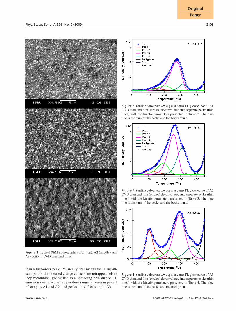
Complementary information about the diamond filmsurface morphology and the growth time was investigatedby SEM. Figure 2 shows the micrographs of the diamondfilm surfaces. The films are composed of sharp well-facetedmicro-crystallites ranging in size from about 0.1 to 2 �mwith many twinned crystallites. They have no evident prefer-ential orientation and the crystal size depended on the growthtime. Film A1 exhibited an inhomogeneous surface growthand smaller size crystallite distribution. This microstructuralcharacteristic may be associated to the observed low inten-sity 1332 cm−1 diamond Raman band and the peaks around1480–1580 cm−1. The A2 and A3 diamond samples micro-graphs shows well-faceted micro-crystallites ranging in sizefrom about 0.5 to 2 �m characteristic of a continuous filmwith well-defined facets composed mainly of diamond, asindicated by its Raman spectrum, and very little non-diamondcomponent. The growth of good quality CVD diamond filmsinvolves, first, nucleation of individual crystallites on thesubstrate surface, then three-dimensional growth of thesecrystallites, faceting and coalescence with neighboring crys-tallites, and finally growth of a continuous polycrystallinediamond layer. This growth process is very likely happeningas depicted by series of SEM micrographs showed: in theA1 sample the growth time was too short to produce a con-tinuous diamond film, whereas in A2 and A3 the films hadcoalesced.
TL characterization was carried out using a home-madedeconvolution program based on the non-linear least-squareMarquardt method from which the kinetic parameters wereextracted. The curve-fitting method, described in detailedelsewhere [10], was performed to obtain the best fit to exper-imental data, assuming a given number of general orderkinetics peaks. Therefore, the best fit provided the kineticorder and values for the activation energy E (eV) and fre-quency factor s (s−1). The best fits are shown in Figs.3–5 and the values of the kinetic parameters are shown inTables 2–4.
The TL glow curve shapes in all samples are character-ized by a dominant TL peak around 250–300 ◦C and a lessintense peak in the 100–145 ◦C low-temperature region. Thelow-temperature components all obey second-order kineticsand are located around 100–145 ◦C. The dominant TL peaksare of first-order kinetics except for sample A3 that obeyskinetics order of ∼1.6. It should be recalled that a first-orderkinetics process means negligible retrapping during the ther-mal stimulation, and is characterized by an asymmetric TLpeak being wider on the low temperature side than on the hightemperature side, a feature clearly shown in Figs. 3–5. In con-trast, a second-order TL peak is wider and more symmetric
© 2009 WILEY-VCH Verlag GmbH & Co. KGaA, Weinheim www.pss-a.com
Original
Paper
Phys. Status Solidi A 206, No. 9 (2009) 2105
Figure 2 Typical SEM micrographs of A1 (top), A2 (middle), andA3 (bottom) CVD diamond films.
than a first-order peak. Physically, this means that a signifi-cant part of the released charge carriers are retrapped beforethey recombine, giving rise to a spreading bell-shaped TLemission over a wider temperature range, as seen in peak 1of samples A1 and A2, and peaks 1 and 2 of sample A3.
Figure 3 (online colour at: www.pss-a.com) TL glow curve of A1CVD diamond film (circles) deconvoluted into separate peaks (thinlines) with the kinetic parameters presented in Table 2. The blueline is the sum of the peaks and the background.
Figure 4 (online colour at: www.pss-a.com) TL glow curve of A2CVD diamond film (circles) deconvoluted into separate peaks (thinlines) with the kinetic parameters presented in Table 3. The blueline is the sum of the peaks and the background.
Figure 5 (online colour at: www.pss-a.com) TL glow curve of A3CVD diamond film (circles) deconvoluted into separate peaks (thinlines) with the kinetic parameters presented in Table 4. The blueline is the sum of the peaks and the background.
www.pss-a.com © 2009 WILEY-VCH Verlag GmbH & Co. KGaA, Weinheim
ph
ysic
a ssp stat
us
solid
i a
2106 R. Melendrez et al.: Thermoluminescence assessment of HFCVD undoped diamond films
Table 2 Kinetic parameters for A1 CVD diamond film.
peak temperature ofmaximum (◦C)
kineticorder
activationenergy (eV)
frequencyfactor (s−1)
1 143 2 0.55 3.3 × 10⁵
2 203 1 0.53 2.2 × 10⁴
3 274 1 0.74 3.7 × 10⁵
4 315 1.6 1.61 7.2 × 10¹²
Table 3 Kinetic parameters for A2 CVD diamond film.
peak temperature ofmaximum (◦C)
kineticorder
activationenergy (eV)
frequencyfactor (s−1)
1 114 2 0.43 2.3 × 10⁴
2 192 1 0.51 1.8 × 10⁴
3 256 1 0.78 2.1 × 10⁶
4 311 1.6 1.12 3.5 × 10⁸
Table 4 Kinetic parameters for A3 CVD diamond film.
peak temperature ofmaximum (◦C)
kineticsorder
activationenergy (eV)
frequencyfactor (s−1)
1 106 2 0.78 2.9 × 10⁹
2 159 2 0.72 2.3 × 10⁷
3 232 1 0.68 3.7 × 10⁵
4 294 1.6 0.97 2.9 × 10⁷
5 374 1 0.93 8.5 × 10⁵
Several studies have shown that CVD diamond filmsexhibit very different TL glow peak structures depending ontheir growth parameters, impurities, and doping materials.Since TL is very sensitive to defects and impurity-relatedcenters, it is a difficult task to assign a TL glow peak to aparticular impurity or defect. However, the glow curve shapefor most synthetic CVD diamonds seems to be composed ofone or two main bands peaked at 50–150 and 200–350 ◦C,along with some overlapped structure of different intensitiesTL peaks [2–15]. The TLD performance of CVD diamondhas been tested in a number of diamond samples of diverseorigin. For example, a batch of 20 CVD diamond samplesfrom the same wafer, from Institute of Material Researchat Limburg University, Belgium, showed a non-reproducible30% discrepancy TL response without previous annealing[5, 8]. The TL variations and fluctuation diminished after1 h annealing at 400 ◦C before irradiation. The TL varia-tions were attributed to a non-homogeneous distribution ofdopant concentration across the CVD wafer from whichthe examined samples came. Other authors investigated theTL properties of ten CVD diamond specimens and foundaround 5% TL reproducibility and sensitivity comparable tocommercial LiF dosimeters, although no batch homogene-ity was reported [16, 17]. Six high-quality CVD diamondcut from the same wafer obtained from De Beers Industrial
Diamonds (UK) Ltd. exhibited a 2% reproducibility over tenTL measurements and an average of 6.1% for the six sam-ples [3]. A more recent comparative investigation on the TLproperties focused on clinical dosimetry, established 3% TLmeasurement reproducibility on 20 CVD diamond samplessynthesized by the Naval Research Laboratory. The samplesshowed a remarkable ±5% TL sensitivity from the meanvalue, which was five times higher than that of the commer-cially available TLD 100 dosimeter [18]. It is to be noted thatsome of the large 2–30% reproducibility differences may bedue to the TL read-out protocols used, annealing conditionsas well as local environmental disturbance. There is a generalagreement that TL glow curve features and dosimetry perfor-mance originates from the CVD diamond crystallographicdefects and centers as a result of extrinsic substitutionalimpurities or intrinsic-like interstitials introduced during thegrowth process.
The effect of nitrogen incorporation in CVD diamondfilms during growth on the TL performance has been under-taken with the expectation that this may control the trappinglevel population to improve the TL sensitivity, reproducibil-ity, and dose linearity [19–21]. Indeed, optimization of the TLintensity and dose linearity were found through incorpora-tion of 20 ppm nitrogen concentration in the gas phase [20].However, the TL glow curve had different shapes depend-ing on nitrogen concentration. The low-temperature peak,clearly observed for low or zero nitrogen incorporation,decreased for higher nitrogen concentration. In addition, thehigh-temperature peak shifted from 230 to 250 ◦C when thenitrogen concentration incorporated into the diamond filmincreased, except for a nitrogen concentration of 20 ppmwhere the peak position remained at 230 ◦C. Also, a 20 ppmnitrogen concentration increased the TL dose saturationregion form about 1 Gy (undoped) to about 40 Gy, whichis a remarkable improvement with respect to undoped dia-mond samples. Further studies in the same set of samplesusing micro-Raman spectroscopy and secondary ion massspectroscopy identified the contribution of graphitic phasesand DLC or amorphous carbon for samples with a 2%[N2/H2] concentration in the gas phase [21]. The nitrogenluminescence bands corresponding to an interstitial nitrogenatom bonded to the nearest vacancy and to the NV sys-tem (vacancy trapped at a substitutional nitrogen atom) wereidentified. A significant finding established from the samework [21] was that shallow levels, corresponding to near-room-temperature peaks, were associated with low nitrogenincorporation, while the high-temperature peak, correspond-ing to deep levels were characteristic of higher nitrogenincorporation samples.
The relative TL glow curve peak intensities and shift-ing of its temperature maxima as a function of incorporatednitrogen concentration has also been observed in nominallypure CVD samples in which no nitrogen has been incorpo-rated [19]. The films were unintentionally contaminated withnitrogen from air leaks or impurities in reactants. However,nitrogen concentrations were estimated to be in the range of5–26 ppm, producing a TL increase in the low-temperature
© 2009 WILEY-VCH Verlag GmbH & Co. KGaA, Weinheim www.pss-a.com

Original
Paper
Phys. Status Solidi A 206, No. 9 (2009) 2107
peak, optimized around 10 ppm, along with a TL inten-sity decrease in the rest of the observed TL peaks as thenitrogen concentration increased. Therefore, even traces orextremely low nitrogen doping levels, may cause strongeffects on the TL glow curve shape modifying the popu-lation and trapping-level distribution in CVD diamond films.Boron-doped CVD diamond films enhance around 25% theTL sensitivity in concentrations below 15 ppm with respectto undoped samples. However, for higher boron concentra-tions (>15 ppm) the high-temperature glow peaks decreasedrastically and low-temperature peak component appearsaround 70 ◦C [22].
It should be recalled that the main consequence of nitro-gen or boron incorporation is to change the morphology anddefect content of the films [23, 24], which are responsible forthe thermally stimulated luminescence (TL), current (TSC),and exoelectronic emission (TSEE) associated with defectformation during growing and localized levels within thegap [25, 26]. The presence of structural defects and compo-sitional impurities, which, of course, depend on the growthconditions, strongly affects the charge transport, collectionefficiency and trapping population, and causes evident effectson the TL glow curve. It is also important to stress the fact thateven traces of nitrogen or boron impurities may have a strongeffect on the morphology and defect formation on the CVDdiamond samples. Therefore, the TL glow curves shown inFigs. 3–5 may contain different nitrogen (or boron) featureslinked to nitrogen-related defects with changing morphologycharacteristics as the growth time increases.
The high-intensity TL glow peak around 250–300 ◦Cobserved in the CVD diamond samples shown in Figs. 3–5has also been observed by other authors, but peaked at around267 [2, 11, 18, 30], 247 [19, 21], and 287 ◦C [21] overlappedby a broad spectral TL 400–600 nm emission band attributedto the well-known A-band associated with donor–acceptorrecombination pairs [22], where the donor would be nitrogenand the acceptor boron [19]. The A-band has been observedin natural and synthetic diamond as a broad 590–413 nm band[27]. The glow peak components with their activation ener-gies are shown in Tables 2–4, and are in agreement withpreviously reported data. The differences may be accountedfor by the particular TL read-out protocol or the glow curvedeconvolution used. Although some TL glow peaks havebeen ascribed to the presence of nitrogen or boron, additionalinvestigation is required due to the complexity of defects andcenter formation.
The detection of defects and centers requires the useof high resolution spectroscopic techniques, like photolu-minescence (PL), cathodoluminescence (CL), or ion beaminduced luminescence (IBIL), which may provide conclu-sive identification of the luminescence from defects andcenters in CVD diamond films. At the moment, we haveno spectroscopic information about the samples investigatedhere, and work on this is in progress. However, we haveperformed a very detailed IBIL on several CVD diamondsamples that indicates the presence of different nitrogen-vacancy complexes, even in high-quality nominally undoped
CVD diamond films [27]. Nitrogen-vacancy center emissionscorresponding to [Ns-V-Ns]0, [Ns-V]0, [N-V]n, and [N-V]−
were found in HFCVD and microwave CVD (MWCVD)diamond film specimens [27–31]. The spectrally resolvedTL glow curve, i.e., the TL intensity as a function of emis-sion wavelength and temperature, may provide informationabout the impurities, defects, and radiative recombinationcenters in a CVD diamond film, although with less sensitiv-ity than IBIL [18, 21, 27]. Therefore, the standard TL glowcurve, recorded as a TL intensity-temperature curve, has astrong limitation for the identification of defects and centers.However, as the CVD growth process improves its controlon impurities and morphological features of the depositedfilms, the TL glow curve might become a genuine signatureof the quality of CVD diamond films.
4 Conclusions Synthetic diamond grown by CVD isa very attractive material for TLD applications. In spiteof the large potentialities, like having soft-tissue equiva-lence, chemical stability, and non-toxicity, the growth ofCVD diamond films with tailored TL properties for radiationdosimetry has been a difficult goal to achieve. The reason isthe great number of defects and centers created during growthby impurities materials and instabilities of the CVD reactorparameters. The presence of structural defects and compo-sitional impurities, which depend on the growth conditions,strongly affect the TL response of the CVD diamond film.We have provided evidence that the TL glow curve featureschange as a function of growth time of high-quality HFCVDdiamond films grown under the same reactor conditions. Inspite of the strict control on the growth and precursor gasconditions imposed in the present experiment, we found noobvious correlation between the growth conditions and theTL pattern. This may perhaps be due to the HFCVD methodused, which may produce a great variety of defect complexesresponsible for the irregular TL glow curve features. It isexpected that the MWCVD technique would provide CVDdiamond samples with a more systematic TL behavior. TheTL glow curve structure may be ascribed to nitrogen-vacancycomplexes caused by traces of nitrogen or other contaminantsthat modifies film morphology and crystallinity. Further high-resolution spectroscopy measurements are necessary for aconclusive assignment of the TL peaks to particular defectsor centers.
Acknowledgements The authors acknowledge financialsupport from CONACYT grants nos. 83536 and 82765.
References
[1] R. Chen and S. W. S. McKeever, Theory of Thermolumines-cence and Related Phenomena (World Scientific, Singapore,1997).
[2] M. Benabdesselam, P. Iacconi, D. Briand, and J. E. Butler,Diam. Relat. Mater. 9, 1013 (2000).
[3] S. Mazzocchi, M. Bruzzi, M. Bucciolini, G. Cuttone, S. Pini,M. G. Sabini, and S. Sciortino, Nucl. Instrum. Methods A 476,713 (2002).
www.pss-a.com © 2009 WILEY-VCH Verlag GmbH & Co. KGaA, Weinheim

ph
ysic
a ssp stat
us
solid
i a
2108 R. Melendrez et al.: Thermoluminescence assessment of HFCVD undoped diamond films
[4] B. Marczewska, P. Olko, M. Nesladek, M. P. R. Waligorski,and Y. Kerremans, Radiat. Prot. Dosim. 101, 485 (2002).
[5] B. Marczewska, P. Bilski, M. Nesladek, P. Olko, M. Rebisz,and M. P. R. Waligorski, Phys. Status Solidi A 193, 470 (2002).
[6] J. Pospısil, R. Bulır, Z. Budinska, R. Novak, B. Sopko, V.Spıvacek, T. Cechak, P. Hlıdek, P. Matejka, A. Mackova,A. Cejnarova, and J. Krasa, Phys. Status Solidi A 199, 131(2003).
[7] M. Rebisz, M. J. Guerrero, D. Tromson, M. Pomorski, B. Mar-czewska, M. Nesladek, and P. Bergonzo, Diam. Relat. Mater.13, 796 (2004).
[8] J. Krasa, B. Marczewska, V. Vorlicek, P. Olko, and L. Juha,Diam. Relat. Mater. 16, 1510 (2007).
[9] S. Preciado-Flores, M. Schreck, R. Melendrez, V. Chernov, R.Bernal, C. Cruz Vazquez, F. Brown, and M. Barboza-Flores,Phys. Status Solidi A 202, 2206 (2005).
[10] M. Barboza-Flores, M. Schreck, S. Preciado-Flores, R.Melendrez, M. Pedroza-Montero, and V. Chernov, Phys. StatusSolidi A 204, 3047 (2007).
[11] M. Benabdesselam, P. Iacconi, D. Briand, D. Lapraz, and J. E.Butler, Radiat. Prot. Dosim. 84(1–4), 257, (1999).
[12] B. Marczewska, C. Furetta, P. Bilski, and P. Olko, Phys. Stat.Sol. (A) 185, 183 (2001).
[13] J. Pospısil, R. Novak, B. Sopko, V. Spıvacek, P. Hlıdek, P.Matejka, A. Mackova, A. Cejnarova, L. Juha, and J. Krasa,Phys. Status Solidi A 185, 195 (2001).
[14] C.-C. Liu, J.-P. Lin, and T.-C. Chu, Appl. Radiat. Isot. 59, 79(2003).
[15] J. Krasa, L. Juha, V. Vorlıcek, and A. Cejnarova, Nucl. Instrum.Methods, A 524, 332 (2004).
[16] E. Borchi, M. Bruzzi, C. Leroy, and S. Sciortino, J. Phys. D,Appl. Phys. 31, 609 (1998).
[17] F. Bogani, E. Borchi, M. Bruzzi, C. Leroy, and S. Sciortino,Nucl. Instrum. Methods Phys. Res. A 388, 427 (1997).
[18] M. Benabdesselam, B. Serrano, P. Iacconi, F. Wrobel, D.Lapraz, J. Heralult, and J. E. Butler, Radiat. Prot. Dosim. 120,87 (2006).
[19] M. Benabdesselam, P. Iacconi, J. E. Butler, and D. Briand,Diam. Relat. Mater. 10, 2084 (2001).
[20] C. Descamps, D. Tromson, M. J. Guerrero, C. Mer, E. Rzepka,M. Nesladek, and P. Bergonzo, Diam. Relat. Mater. 15, 833(2006).
[21] C. Descamps, D. Tromson, C. Mer, M. Nesladek, P. Bergonzo,and M. Benabdesselam, Phys. Status Solidi A 203(12), 3161(2006).
[22] M. Benabdesselam, P. Iacconi, D. Briand, D. Lapraz, E.Gheeraert, and A. Deneuville, Diam. Relat. Mater. 9, 56(2000).
[23] A. J. Eccles, T. A. Steele, A. Afzal, C. A. Rego, W. Ahmed,P. W. May, and S. M. Leeds, Thin Solid Films 343, 620(1999).
[24] P. W. May, P. R. Burridge, C. A. Rego, R. S. Tsang, M. N.R. Ashfold, K. N. Rosser, R. E. Tanner, D. Cherns, and R.Vincent, Diam. Relat. Mater. 5, 354 (1996).
[25] D. Briand, P. Iacconi, M. Benabdesselam, D. Lapraz,P. W. May, and C. A. Rego, Diam. Relat. Mater. 9, 1245(2000).
[26] D. Briand, P. Iacconi, M. Benabdesselam, D. Lapraz, R. Bindi,P. W. May, C. A. Rego, and A. Afzal, Thin Solid Films 359,150 (2000).
[27] H. Calvo del Castillo, J. L. Ruvalcaba, E. Belmont, T.Calderon, R. Melendrez, and M. Barboza-Flores, Phys. StatusSolidi A 205, 2221 (2008).
[28] A. M. Zaitsev, Optical Properties of Diamond: A Data Hand-book (Springer, Berlin, 2001).
[29] C. Manfredotti, in: Carbon, The Future Material for AdvancedTechnology Applications, Topics in Applied Physics Vol. 100,edited by G. Messina, and S. Santangelo (Springer, Berlin,Heidelberg 2006), p. 239.
[30] M. Benabdesselam, P. Iacconi, J. E. Butler, and J. M. Nigoul,Diam. Relat. Mater. 12, 1750 (2003).
[31] E. Cruz-Zaragoza, R. Melendrez, V. Chernov, M. Barboza-Flores, and S. Gastelum, Nucl. Instrum. Methods B 248, 103(2006).
© 2009 WILEY-VCH Verlag GmbH & Co. KGaA, Weinheim www.pss-a.com


![Phys. Status Solidi B...way. But in the case of single-wall carbon nanotubes the fluorination degree isC 2F 0.5–0.4 [15] which can be related to surface fluorination of one side](https://img.pdfslide.us/doc/110x75/5f4235311197fd7d0408bc14/phys-status-solidi-b-way-but-in-the-case-of-single-wall-carbon-nanotubes-the.jpg)


![This article has been published In Physica Status Solidi : Rapid … · 2020. 1. 24. · [15] This structural analogy between amorphous and crystal does clearly not hold for PCMs,](https://img.pdfslide.us/doc/110x75/60d48a2a57d11e1ca2173511/this-article-has-been-published-in-physica-status-solidi-rapid-2020-1-24.jpg)