Embed Size (px)
Citation preview

MTL ANNUAL RESEARCH REPORT 2016 Photonics and Optoelectronics 129
Photonics and OptoelectronicsStochastic Simulation and Robust Design Optimization of Integrated Photonic Filters ............................................. 131Germanium Photodetectors on Amorphous Substrates for Electronic-Photonic Integration .................................. 132Superconducting Nanowire Single-photon Detector on Aluminum Nitride ................................................................ 133Temporally and Spatially Resolved Photon-sensing in a Slow-wave Nanowire ............................................................. 134Development of Compact and Scalable Packaging for a Fiber-Coupled Single-Photon Detector Array ........................................................................................................................................... 135Light Modulators for Holographic Video Displays ............................................................................................................ 136Lab-on-Chip Dark-Field Imaging Device with Tunable Emission Profile ...................................................................... 137Low-Loss Planar Chalcogenide Glass Photonics .............................................................................................................. 138On-chip Mid-infrared Gas Detection Using Chalcogenide Glass Waveguide ............................................................. 139Electronic and Optoelectronic Transport of Transitional Metal Dichalcogenides ........................................................ 140High-Responsivity Graphene-Boron Nitride Photodetector in a Silicon Photonic Integrated Circuit .................... 141 High-yield Creation of Diamond Defect Centers in Photonic Crystal Cavities .......................................................... 142Circular Gratings for Efficient Collection from Implanted Silicon Vacancy Centers in Diamond ............................................................................................................................................................................ 143Ultrafast Fluorescent Decay Induced by Metal-mediated Dipole-dipole Interaction in Two-dimensional Molecular Aggregates ........................................................................................................................ 144Foldable and Cytocompatible Sol-gel TiO2 Photonics ................................................................................................... 145Towards Lasing in Colloidal Quantum Dots Using Nanobeam Photonic Crystal Cavities .......................................... 146

130 Photonics and Optoelectronics MTL ANNUAL RESEARCH REPORT 2016

MTL ANNUAL RESEARCH REPORT 2016 Photonics and Optoelectronics 131
Stochastic Simulation and Robust Design Optimization of Integrated Photonic FiltersT. W. Weng, D. Melati, A. Melloni, L. Daniel Sponsorship: NSF
Photonics is rapidly emerging as a mature and promising technology, and it is evolving from a pure research topic to a market-ready player, aiming at achieving large production volumes and small fabrication costs. Pushed by these motivations, process design kits, circuit simulators, generic foundry approaches, and multi-project-wafer runs are quickly changing the way that photonic circuits are conceived and designed. On the other hand, stochastic uncertainties such as fabrication variations are unavoidable in production processes. It is well known that such uncertainties can have a dramatic impact on the functionality of fabricated circuits. In order to obtain a high quality design of a photonic circuit, it is important to include such uncertainties during the early design stages. Hence, uncertainty quantification techniques become fundamental instruments to efficiently obtain the statistical information and to ach-ieve a high-quality design.
Monte Carlo simulation is commonly exploited to evaluate the impact of fabrication uncertainties on the functionality of the designed circuits. Although effective, it suffers from a slow convergence rate and requires long computation time. Meanwhile, stochastic spectral methods have recently been regarded as a promising
alternative for statistical analysis due to their fast convergence. The key idea is to approximate the output quantity of interest (e.g., the bandwidth of a filter) with a set of orthonormal polynomial basis functions, known as generalized polynomial chaos expansion. Our goal in this work is to develop an efficient, robust design-optimization technique based on the state-of-the-art sampled-based stochastic spectral methods, which are mainly used for statistical analysis in the field of uncertainty quantification. Figure 1 shows a fifth-order directly coupled ring resonator used to demonstrate our technique. Due to fabrication process variations, the gap g and effective phase index neff of each ring resonator are uncertain, so the 3dB bandwidth varies greatly. In this example, we would like to design the nominal gap g for each ring that minimizes the mean- square-error of 3dB bandwidth. Figure 2 plots simu-lation results of the un-optimized nominal design and optimized nominal design. We show that the opti-mized circuits are more robust to fabrication process variations and achieve a reduction of 11 % to 35 % in the mean-square-errors of the 3dB bandwidth compared to un-optimized nominal designs.
Figure 1: A 5-ring coupled resonator. Figure 2: Probability density functions of 3dB. Bandwidth if the un-optimized nominal design (blue dash line) and optimized nominal design (red line).
FURTHER READING
• D. Melati, A. Alippi, and A. Melloni, “Waveguide-based Technique for Wafer-level Measurement of Phase and Group Effective Refractive Indices,” Journal of Lightwave Technology, pp. 99:1-1, 2015.
• D. Xiu and G. E. Karniadakis, “Modeling Uncertainty in Flow Simulations via Generalized Polynomial Chaos,” Journal of Computational Physics, vol. 187, pp. 137-167, 2003.

132 Photonics and Optoelectronics MTL ANNUAL RESEARCH REPORT 2016
Germanium Photodetectors on Amorphous Substrates for Electronic-Photonic IntegrationB. S. Pearson, L. C. Kimerling, J. Michel Sponsorship: ARPA-E
Silicon photonics has emerged as a leading technology to overcome the bandwidth and energy efficiency bot-tlenecks of standard metal interconnects. Integration of photonics in the back-end-of-line (BEOL) of a standard CMOS process enables the advantages of optical inter-connects while benefiting from the low-cost of mono-lithic integration. However, processing in the BEOL requires device fabrication on amorphous substrates and constrains processing to ≤450°C. A germanium pho-todetector was fabricated while adhering to these pro-cessing constraints in order to demonstrate a proof of concept for BEOL integration.
Crystalline Ge was grown on SiO2 by selective deposition in geometrically confined channels. The emerging Ge grains were coalesced to fill a lithographically defined trench, forming the active area of a photodetector. The Ge was measured to have a tensile strain of 0.5%, which was caused by thermal expansion mismatch with the substrate, and concentrated by small voids from imperfect
coalescence. The resolved shear stress was determined to be below the critical resolved shear stress, verifying that dislocation generation does not occur in this material. The strain was shown to increase the absorption of Ge at long wavelengths, allowing for implementation along the entire telecom window.
A Schottky barrier to p-type Ge was developed by the addition of a 1-nm tunneling Al2O3 layer between an Al/Ge metal contact. This de-pinned the Fermi level, creating a barrier height of 0.46eV. The Schottky contacts enabled the fabrication of metal-semiconductor-metal (MSM) photodetectors on epitaxial Ge with dark current densities of 2.1 x 10⁻² Acm−2. Gain was observed in these photodetectors, with internal quantum efficiencies (IQE) of 405%. MSM detectors were also made using Ge on SiO2, exhibiting an IQE of 370%. This is the first demonstration of IQE > 100% in a Ge MSM or pin photodetector and proves the feasibility of making high-performance active photonic devices while adhering to BEOL processing constraints.
0 1 2 3 4Voltage [V]
0
0.5
1
1.5
2
2.5
3
3.5
Resp
onsiv
ity [A
/W]
Contact Separation=0.5umContact Separation=1umContact Separation=2um
Figure 1: Plane-view SEM image of coalesced Ge grains that are grown on SiO2 at 450 °C. After planarization, this serves as the active material for BEOL-compatible MSM photodetectors.
Figure 2: Responsivity of crystalline Ge MSM photodetectors with different contact separations under 980-nm illumination. An IQE of 405% is measured at a bias of 4 V and contact separation of 0.5 µm.

MTL ANNUAL RESEARCH REPORT 2016 Photonics and Optoelectronics 133
Superconducting Nanowire Single-photon Detector on Aluminum NitrideD. Zhu, H. Choi, T.-J. Lu, Q. Zhao, A. Dane, F. Najafi, D. R. Englund, K. K. Berggren Sponsorship: DARPA, AFOSR, NSF
Superconducting nanowire single-photon detectors (SNSPDs) offer high detection efficiency, low timing jitter, low dark counts, short reset time, and broad spec-tral response. This unique combination of properties has made SNSPDs an attractive choice for quantum information processing applications. Recent advanc-es in photonic integrated single-photon sources and quantum memories have created increasing demand for on-chip integration of high performance SNSPDs, toward realizing a complete on-chip photonic quantum processor. Among various waveguide materials, alumi-num nitride (AlN) stands out as a promising candidate. It has a broad spectral window of transparency, intrin-sic electro-optic and piezoelectric properties, and a low fluorescence rate. To date, direct fabrication of high efficiency SNSPDs on AlN has not been demonstrated.
We have now successfully fabricated high-efficiency niobium nitride (NbN) SNSPDs on AlN-on-sapphire substrates. The NbN thin films were deposited using reactive DC magnetron sputtering at 840OC. The films had a thickness of ~5 nm, critical temperature of
10.6–11.4K, and sheet resistance of 500–550 Ω/square. We adopted a 2-element superconducting nanowire avalanche photodetector (2-SNAP) design with 60-nm wire width to achieve high quantum efficiency and signal-to-noise ratio. Figure 1 shows scanning electron micrographs (SEM) of fabricated devices. The devices were tested at 2.45K under 1550-nm illumination and showed saturated detection efficiency (an indication of high internal quantum efficiency), sub-60-ps jitter, and
~6 ns reset time (see Figure 2). The devices were designed for integration on AlN single mode waveguides operating at 637-nm wavelength, corresponding to the zero-photon line of nitrogen vacancy centers in diamond. Since the quantum efficiency of SNSPDs increases with photon energy, we expect more prominent saturation behavior at 637 nm. We are now working towards fabricating AlN waveguides on the detector chips and integrating single-photon sources and quantum memories to realize a full single-photon quantum circuit.
Figure 1: (a) SEM of the fabricated device. (b) The serial in-ductor region, made of 300-nm-wide meander nanowires. (c) The active region of the detector, which consists of two parallel nanowires with 60-nm width, 80-nm gap, and 22-μm length.
Figure 2: Detection efficiency and background count rate vs. bias current. The detection efficiency enters the saturation region when bias current ap-proaches the switching current. The absolute value in DE was limited by the unpolished back surface of the chip.
FURTHER READING
• G. N. Gol’tsman, O. Okunev, G. Chulkova, A. Lipatov, A. Semenov, K. Smirnov, B. Voronov, A. Dzardanov, C. Williams, and R. Sobolewski, “Picosecond Superconducting Single-photon Optical Detector,” Appl. Phys. Letters, vol. 79, pp. 705, 2001.
• C. Xiong, W. H. P. Pernice, X. Sun, C. Schuck, K. Y. Fong, and H. X. Tang, “Aluminum Nitride as a New Material for Chip-scale Optomechanics and Nonlinear Optics,” New Journal of Physics, vol. 14, no. 9, pp. 095014, 2012.
• F. Marsili, F. Bellei, F. Najafi, A. E. Dane, E. A. Dauler, R. J. Molnar, and K. K. Berggren, “Efficient Single Photon Detection from 500 nm to 5 μm Wavelength,” Nano Letters, vol. 12, pp. 4799–4804, 2012.

134 Photonics and Optoelectronics MTL ANNUAL RESEARCH REPORT 2016
Temporally and Spatially Resolved Photon-sensing in a Slow-wave NanowireQ. Zhao, D. Zhu, N. Calandri, F. Bellei, A. N. McCaughan, A. E. Dane, H. Wang, D. F. Santavicca, K. K. Berggren Sponsorship: NSF, AFOSR
We have demonstrated spatially- and time-resolved photon counting in a single superconducting nanowire, which was designed as a slow-wave transmission line. We were able to discriminate where and when photons landed along a continuous nanowire of 20-mm-long and 300 nm wide. Instead of using an array of discrete photodetectors to acquire an optical image, the slow-wave nanowire (SWN) is meandered into a 286 μm × 193 μm square and has an equivalent pixel number of over 300. In addition to this spatial resolution, the arrival time of each photon was simultaneously resolved with a timing jitter of 100 ps for photons with a wavelength of 1.5 μm.
The spatial and temporal photodetection infor-mation was read out by measuring the difference and sum of the pulse arrival times on the nanowire’s two outputs, respectively. This method was possible
because we designed our superconducting nanowire such that it behaved not only as a single-photon detector, but also as a slow-wave transmission line. When a photon is absorbed, creating a hotspot, two electrical pulses are generated and propagate towards the two ends of the nanowire. By measuring the arrival times of the two electrical pulses, we determined the location of photon absorption from the difference and the photon arrival time from the sum. Signals propagate along the nanowire at a velocity of several percent of the speed of light, tens of times slower than an identical transmission line made from normal metals because the nanowire has high kinetic inductance. Combining the slow-wave transmission line with our 3 ps electrical timing uncertainty allows us to determine the position at which the photon was observed to a precision of 30 μm.
Figure 1: SEM image of the slow-wave nanowire. We de-signed the nanowire into a coplanar waveguide. The signal line, a 300-nm-wide nanowire with a 100-nm-wide gap to the ground plan, is made from the same NbN film. The total length of the slow-wave nanowire (SWN) is 20 mm.
Figure 2: An optical image taken by the slow-wave nanowire. The wavelength of the light used is 780 nm. A metal mesh with a period of 75 μm was put on top of the imager to create this pattern.
FURTHER READING
• Q. Zhao, A. McCaughan, F. Bellei, F. Najafi, D. De Fazio, A. Dane, Y. Ivry, and K. K. Berggren, “Superconducting-nanowire Single-photon-detector Linear Array,” Appl. Phys. Letters, vol. 103, no. 14, pp. 142602, 2013.
• H. T. Su, Y. Wang, F. Huang, and M. J. Lancaster, “Superconducting Delay Lines,” Journal of Supercond. Nov. Magn., vol. 21, pp. 7–16, 2008.

MTL ANNUAL RESEARCH REPORT 2016 Photonics and Optoelectronics 135
Development of Compact and Scalable Packaging for a Fiber-Coupled Single-Photon Detector ArrayF. Bellei, D. Zhu, H. Choi, L. Archer, J. Mower, D. Englund, K. K. Berggren Sponsorship: ONR, DARPA, AFOSR
Superconducting nanowire single-photon detectors (SNSPDs) combine high speed, low timing jitter, and high detection efficiency, making them suitable for quantum-secured communications. We are developing a package to couple an array of single-mode 1550-nm-wave-length optical fibers to an array of SNSPDs. Unlike previ-ous coupling methods, our design uses the high density of single-mode fiber arrays to integrate eight detectors, coupled one-to-one, to optical fibers within an area < 1 cm × 1 cm. Figure 1(a) shows the CAD design of the package. The fiber array was glued to the SNSPD chip and attached to a copper mount with a clamp. The chip was wire-bonded to an eight-channel PCB for read-out. The copper mount was designed to mount in a closed-cy-cle cryostat. Figure 1(b) shows a schematic of the align-ment method. The detectors were spaced on the chip to match the pitch of the fiber array.
The SNSPD chip and the fiber array were aligned using an IR imaging system. After gluing we dipped the chip and array in liquid helium and verified that the glue resisted the thermal cycling. We fabricated a 32-element series-2-superconducting nanowire avalanche photodetector) array with 250-µm pitch matching the 32-element fiber array spacing. The fiber array was controlled on two rotational axes and one translational axis. The chip was controlled on the two orthogonal translational axes for a total control on five axes. We are currently integrating the detector chip in a cryostat with base temperature of 2.9 K, which will become the eight-channel single-photon receiver. We will use this system in flood-light quantum key distribution experiment.
Figure 1. (a) CAD design of the package holding the SNSPD chip and fiber array. (b) Schematic of three detectors of the SNSPD array aligned to three elements of the fiber array. We use the high precision of micro-fabrication techniques to match the detectors’ spacing to the fibers’ pitch.
FURTHER READING
• G. N. Gol’tsman, O. Okunev, G. Chulkova, A. Lipatov, A. Semenov, K. Smirnov, B. Voronov, A. Dzardanov, C. Williams, and R. Sobolewski, “Picosecond Superconducting Single-photon Optical Detector,” Appl. Phys. Letters, vol. 79, no. 6, pp. 705, 2001.
• F. Bellei, A. P. Cartwright, A. N. McCaughan, A. E. Dane, F. Najafi, Q. Zhao, and K. K. Berggren, “Free-space-coupled Superconducting Nanowire Single-photon Detectors for Infrared Optical Communications,” Opt. Express, vol. 24, no. 4, pp. 3248, February 2016.

136 Photonics and Optoelectronics MTL ANNUAL RESEARCH REPORT 2016
Light Modulators for Holographic Video DisplaysV. M. Bove, Jr., S. Jolly, N. Savidis, B. Datta Sponsorship: MIT Media Lab Research Consortium, Center for Terrestrial Sensing, AFRL
In this research (a collaboration with Dr. Daniel Smalley of Brigham Young University), we design and fabricate acousto-optic, guided-wave modulators in proton-ex-changed lithium niobate for use in holographic and oth-er high-bandwidth displays. Guided-wave techniques make possible the fabrication of modulators that are higher in bandwidth and lower in cost than analogous bulk-wave acousto-optic devices or other spatial light modulators used for diffractive displays; these tech-niques enable simultaneous modulation of red, green, and blue light. In particular, we are investigating mul-
tichannel variants of these devices with an emphasis on maximizing the number of modulating channels to achieve large total bandwidths. To date, we have demon-strated multichannel full-color modulators capable of displaying holographic light fields at standard-defini-tion television resolution and at video frame rates. Fig-ures 1 and 2 show a schematic diagram of our device and an image displayed using it, respectively. Our current work explores a variant of this technology that is suitable for wearable holographic displays, fabricated using femtosecond laser micromachining.
Figure 1: Diagram of our modulator (one channel). Figure 2: Color holographic image displayed using our modulator.
FURTHER READING
• D. E. Smalley, Q. Y. J. Smithwick, V. M. Bove, Jr., J. Barabas, and S. Jolly, “Anisotropic Leaky-mode Modulator for Holographic Video Displays,” Nature, vol. 498, pp. 313-317, 2013.
• N. Savidis, S. Jolly, B. Datta, T. Karydis, and V. M. Bove, Jr., “Fabrication of Waveguide Spatial Light Modulators via Femtosecond Laser Micromachining,” SPIE Advanced Fabrication Technologies for Micro/Nano Optics and Photonics IX, pp. 9759, 2016.
• S. Jolly, N. Savidis, B. Datta, V. M. Bove, Jr., and D. Smalley, “Progress in Off-plane Computer-generated Waveguide Holography for Near-to-eye 3D Display,” SPIE Practical Holography XXX: Materials and Applications, pp. 9771, 2016.

MTL ANNUAL RESEARCH REPORT 2016 Photonics and Optoelectronics 137
Lab-on-Chip Dark-Field Imaging Device with Tunable Emission ProfileC. Chazot, Y. Kim, I. Coropceanu, M. Bawendi, M. Kolle Sponsorship: MTL, MISTI
Dark-field microscopy is a well-known imaging technique used to enhance the contrast in unstained samples by suppressing low spatial frequency contributions (areas of uniform intensity), thereby emphasizing high spatial frequency components (for instance edges) in the image. The sample is illuminated with light incident on the sample at a high angle that is not collected by the objective lens, unless it is scattered by the imaged object. Even though it is a simple method that provides high-quality images, it usually requires a classic bulky optical microscope, with dedicated objectives and filtering cubes. Here, we present research aimed at creating a lab-on-chip dark-field imaging device, which can provide dark-field imaging capabilities without the need for sophisticated equipment. We produce a micro-patterned fluorescent surface with a spatially tunable light emission profile, consisting of quantum dots in a polymer matrix sandwiched between a Bragg reflector on the top and semi-spherical micro-concavities at the bottom. While the quantum dots emit light in all directions, the confinement between the Bragg mirror and the semi-spherical cavities allow light to exit from
the surface only in a limited angle range. The color of the emitted light is determined by the quantum dots’ emission spectrum, while directionality is imposed by the stop band of the Bragg reflector. Tuning of the Bragg reflector band-gap, or the combination of Bragg reflectors with different band-gaps, allows for the creation of a rich variety of light emission profiles. To maximize light emission in the desired limited angle range, an array of bioinspired, hexagonally arranged semi-spherical gold micro-reflectors is used. Each patterned surface measures 1” x 1”, and more than 10 Bragg reflectors can be assembled on it, providing the same number of dark-field imaging ring profiles. A sample placed on top of the surface will be illuminated with light of the desired angular distribution only, which for dark-field imaging would be at angles larger than the numerical aperture of the imaging objective. This surface with tailorable light emission profiles constitutes a highly compact, simple, tunable solution for dark-field imaging, and it could for instance find application in miniaturized imaging devices for microbiology.
Figure 1: a) Schematic of the design. From bottom to top: semispherical gold reflector, quantum dots in PMMA, and Bragg reflector. b) Scheme of principle for the amplification of the ring of light with the patterned surface. c) Angle dependence of the reflectivity of a Bragg reflector centered at 585 nm in oil (n=1.5). The blue and the red-hatched regions represent the absorption and emission, respectively, of the quantum dots.
Figure 2: a) SEM cross-sectional view of the device. b) Top view of the device. c), d) Comparison of the c) Modelled ring profile with the d) experimental one for a Bragg reflector centered at 585 nm in oil. e), f) Comparison of the e) modelled ring profile with the f) experimental one for a Bragg reflector centered at 643 nm in oil. g), h) Imaging of a scale of the Papilio Blumei butterfly with g) bright field imaging and h) surface-enabled dark-field imaging.
FURTHER READING
• M. Kolle, P. M. Salgard-Cunha, M. R. J. Scherer, F. Huang, P. Vukusic, S. Mahajan, J. J. Baumberg, and U. Steiner, “Mimicking the Colourful Wing Scale Structure of the Papilio Butterfly,” Nature Nanotechnology, vol. 5, no. 7, pp. 511-515, 2010.

138 Photonics and Optoelectronics MTL ANNUAL RESEARCH REPORT 2016
Low-Loss Planar Chalcogenide Glass PhotonicsQ. Du, Y. Huang, J. Li, D. Kita, J. Michon, H. Lin, L. Li, C. Smith, K. Richardson, W. Zhang, J. Hu Sponsorship: NSF, DOE
Chalcogenide glasses (ChGs) are widely recognized as the material of choice for sensing, flexible substrate in-tegration and all-optical signal processing due to their broad transparency window in the infrared region, low processing temperature, and high Kerr nonlinearity. In addition, their high refractive indices enable small optical mode volume without suffering from excessive radiative loss. Nevertheless, unlike standard integrated photonic materials with well-established processing protocols such as silicon and silica, planar processing of ChGs remains much less mature despite their excep-tional optical properties.
The ChG devices were fabricated on 6” silicon wafers with 3-µm thermally grown oxide coating. A piranha clean was performed prior to film deposition to ensure pristine wafer surface quality. Subsequently, Ge23Sb7S70 (GSS) bulk glass was thermally evaporated
onto the wafer to form a 450-nm-thick ChG film. A 400-nm-thick ZEP resist was then spun onto the glass film and exposed on an Elionix ELS-F125 e-beam system. The resist was then developed by rinsing in ZED-N50 to reveal the patterns. Reactive-ion etching was then carried out on a PlasmaTherm RIE etcher with fluorine chemistry. Channel waveguides were fabricated by etching through the entire GSS layer. After etching, remaining resists were stripped by soaking the sample in N-Methyl-2-pyrrolidone. The fluorine-etched samples underwent an additional oxygen plasma treatment step to remove the fluorocarbon polymer deposited on the waveguide sidewalls formed during the plasma process. SEM images of the waveguide are shown in Figures a and and the transmission of the waveguide resonator is provided in Figure c. We successfully demonstrated a record high Q on chip ChG resonator of 1.2 × 10⁶.
Figure 1: a) SEM top view of GSS waveguide. b) cross- sectional view, and c) transmission spectrum of the waveguide resonator.
FURTHER READING
• L. Li, H. Lin, S. Qiao, Y. Zou, S. Danto, K. Richardson, J. D. Musgraves, N. Lu, and J. Hu, “Integrated Flexible Chalcogenide Glass Photonic Devices,” Nat. Photonics, vol. 8, pp. 643-649, 2014.
• J. Hu, L. Li, H. Lin, Y. Zou, Q. Du, C. Smith, S. Novak, K. Richardson, and J. D. Musgraves, “Chalcogenide Glass Microphotonics: Stepping into the Spotlight,” Am. Ceram. Soc. Bull. vol. 94, pp. 24-29, 2015.
• Y. Chen, H. Lin, J. Hu, and M. Li, “Heterogeneously Integrated Silicon Photonics for the Mid-infrared and Spectroscopic Sensing,” ACS Nano, vol. 8, pp. 6955-6961, 2014.
a) b) c)

MTL ANNUAL RESEARCH REPORT 2016 Photonics and Optoelectronics 139
On-chip Mid-infrared Gas Detection Using Chalcogenide Glass WaveguideZ. Han, P. Lin, V. Singh, L. C. Kimerling, J. Hu, K. Richardson, A. Agarwal, D. T. H. Tan Sponsorship: Ministry of Defense, Singapore
We demonstrate an on-chip sensor for room-tempera-ture detection of methane gas using a broadband spiral chalcogenide glass waveguide coupled with an off-chip laser and detector. The waveguide is fabricated using UV lithography patterning and lift-off after thermal evaporation. We measure the intensity change due to the presence and concentration of methane gas in the mid-infrared (MIR) range.
The GeSbS waveguide is fabricated by thermal evaporation and patterned by contact mask and UV lithography in MTL’s Exploratory Materials Laboratory (EML). A polydimethylsiloxane (PDMS) chamber is
placed on top of the waveguide that holds the gas. We use a spiral-structure design to increase the interaction length, and we use tapered waveguide structures to avoid high absorption loss at the intersection of the polymer chamber sidewall with the chalcogenide glass waveguide. The methane absorption peak at 3310 nm is used to quantify methane concentration in nitrogen down to 2.5 vol. %. At 3310 nm the calculated absorbance per centimeter of methane calculated from the experimental data is 1.9, which matches the value from the NIST spectral database. This work provides an approach for broadband planar MIR gas sensing.
WFigure 1: (a) Top view SEM image of a 2-µm-wide single-mode spiral waveguide. (b) A schematic representation of the waveguide design. At the juncture where light crosses the PDMS gas chamber sidewall, the waveguide is 15 µm wide to better con-fine the light within the waveguide and decrease the absorption loss from PDMS. Within the chamber, the waveguide is tapered down to a single-mode width of 2 µm to enhance evanescence, which leads to enhanced gas-photon interaction.
Figure 2: Transmittance with different methane concentrations. Y-axis is shown in log scale. At 3310 nm, optical transmission for different methane concentrations is measured, showing a responsivity of 0.77.
FURTHER READING
• Z. Han, P. Lin, V. Singh, L. C. Kimerling, J. Hu, K. Richardson, A. Agarwal, and D. T. H. Tan, “On-chip Mid-infrared Gas Detection Using Chalcogenide Glass Waveguide,” Applied Physics Letters, Cambridge: Cambridge University Press, vol. 108, pp. 141106, 2016.
• P. T. Lin, V. Singh, J. Wang, H. Lin, J. Hu, K. Richardson, J. D. Musgraves, I. Luzinov, J. Hensley and L. C. Kimerling, “Si-CMOS Compatible Materials and Devices for Mid-IR Microphotonics,” Optical Materials Express, vol. 3, no. 9, pp. 1474-1487, 2013.
• Y. Chen, H. Lin, J. Hu, and M. Li, “Heterogeneously Integrated Silicon Photonics for the Mid-infrared and Spectroscopic Sensing,” ACS Nano, vol. 8, no. 7, pp. 6955-6961, 2014.

140 Photonics and Optoelectronics MTL ANNUAL RESEARCH REPORT 2016
Electronic and Optoelectronic Transport of Transitional Metal DichalcogenidesY. Yang, Q. Ma, J. I. J. Wang, Y.-A. Cheng, K. Watanabe, T. Taniguchi, H. O. H. Churchill, P. Jarillo-Herrero Sponsorship: ONR, AFOSR, DOE
We are investigating electronic and optoelectronic devic-es based on atomically thin two-dimensional semicon-ductors such as the transistion metal dichalcogenides MoS2 and WSe2. These materials are interesting because they may display new basic physical phenomena not presenting in other materials. Only three atoms thick, they are inherently flexible and transparent materials. We characterize their electronic transport properties and potential for optoelectronic applications. To mea-sure the transport properties of dichalcogenide devices as a function of temperature, we must make low-resis-tance electrical contacts to the material. To achieve this, we encapsulate few-layer WSe22 in hexagonal boron
nitride that has been patterned to allow ionic liquid doping of the contact region (Figure 1). This technique simultaneously protects the WSe2 surface above and below, resulting in the highest mobility few-layer WSe2 devices reported to date.
In addition, due to the ultrathin nature of the devices, interlayer transport across different two-dimensional materials becomes very efficient and reveals unique properties. For instance, the vertical MoS2-BN-graphene van der Waals heterostructure exclusively allows hole transport (after optical excitation) across the BN barrier based on the band alignment, which could lead to novel functionalities (Figure 2).
Figure 2: MoS2-BN-graphene verti-cal photocurrent. (a) Schematic of the measurement. (b) Vertical photocur-rent as a function of the interlayer volt-age and excitation photon energy.
Figure 1: WSe2 electronic transport. (a) Contact resistance and (b) Hall mobility at 220 K. (c) Schematic and (d) Optical image of the device.
FURTHER READING
• J. I. Wang, Y. Yang, Y. Chen, K. Watanabe, T. Taniguchi, H. O. H. Churchill, and P. Jarillo-Herrero, “Electronic Transport of Encapsulated Graphene and WSe2 Devices Fabricated by Pick-up of Pre-patterned hBN,” Nano Letters, vol. 15, no. 3, pp 1898–1903, 2015.

MTL ANNUAL RESEARCH REPORT 2016 Photonics and Optoelectronics 141
High-Responsivity Graphene-Boron Nitride Photodetector in a Silicon Photonic Integrated CircuitR.-J. Shiue, Y. Gao, C. Peng, J. Goldstein, D. K. Efetov, D. R. Englund Sponsorship: EFRC Center for Excitonics
The remarkable electrical and optical properties of graphene are promising for efficient optoelectronic de-vices. However, a long-lasting issue in graphene-based devices is a relatively low absorption coefficient, which is 2.3% due to its ultra-thin thickness. To enhance the light-matter interaction in this single atomic layer ma-terial, graphene has been integrated into optical wave-guides and cavities. By coupling graphene to the guided mode in a silicon waveguide, previously demonstrated graphene photodetectors can exhibit a maximum ab-sorption of 60% of the input light with a maximum of responsivity of 0.1 A/W.
In this work, we demonstrate a graphene-hexagonal boron nitride (hBN) photodetector integrated with a silicon waveguide. In addition to the enhanced absorption of graphene on top of a waveguide, an extra gate terminal serves to manipulate the Fermi energy (EF) in graphene to assist the separation of photo-excited carriers. The maximum responsivity of the device is 0.36 A/W, corresponding to an internal quantum efficiency of 15% at zero source-drain bias voltage (VDS). At high
frequencies, the device exhibits a 3dB cut-off frequency at 42 GHz.
Figure 1 shows the schematic of the graphene-hBN photodetector. Encapsulated single-layer graphene was transferred onto a silicon waveguide using a van der Waals (vdW) assembly technique. Two metal contacts (source and drain) were deposited on graphene to extract photocurrent. An extra gate metal electrode was deposited 50 μm away from the graphene channel. We then coated a layer of polymer electrolyte (Poly(ethylene oxide) plus LiClO4) on the entire sample to control the carrier densities in graphene via the gate electrode. Tuning VGS and VDS can adjust the potential profile of the metal-graphene junction to achieve different internal quantum efficiencies of the photodetector. We measured a maximum responsivity of 0.36 A/W at VGS = 2 V and VDS = 1.2 V, as shown in Figure 2. The six-fold pattern of the photocurrent mapping indicates a strong photothermoelectric (PTE) effect for the photocurrent generation.
Figure 1: Schematic of a waveguide-integrated graphene-bo-ron nitride photodetector. Single layer graphene (SLG) is encap-sulated by top and bottom hexagonal boron nitride (hBN) layers.
Figure 2: Photocurrent mapping of the waveguide-in-tegrated graphene photodetector as a function of gate-souce (VGS) and drain-source (VDS) voltages.
FURTHER READING
• R.-J. Shiue, Y. Gao, Y. Wang, C. Peng, A. Robertson, D. K. Efetov, S. Assefa, F. Koppens, J. Hone, and D. Englund, “High-Responsivity Graphene-Boron Nitride Photodetector and Autocorrelator in a Silicon Photonic Integrated Circuit,” Nano Letters, vol. 15, pp. 7288-7293, 2015.
• Y. Gao, R.-J. Shiue, X. Gan, L. Li, C. Peng, I. Meric, L. Wang, A. Szep, D. Walker Jr., J. Hone, and D. Englund, “High-Speed Electro-Optic Modulator Integrated with Graphene Boron-Nitride Heterostructure and Photonic Crystal Nanocavity,” Nano Letters, vol. 15, pp. 2001-2005, 2015.
• X. Gan, R.-J. Shiue, Y. Gao, I. Meric, T. F. Heinz, K. Shepard, J. Hone, S. Assefa, and D. Englund, “Chip-Integrated Ultrafast Graphene Photodetector with High Responsivity,” Nature Photonics, vol. 7, pp. 883-887, 2013.

142 Photonics and Optoelectronics MTL ANNUAL RESEARCH REPORT 2016
High-yield Creation of Diamond Defect Centers in Photonic Crystal CavitiesT. Schröder, L. Li, M. Walsh, M. E. Trusheim, I. Bayn, J. Zheng, S. Mouradian, H. Bakhru*, D. R. Englund *SUNY Polytechnic InstituteSponsorship: AFOSR PECASE, AFOSR Quantum Memories MURI, ARL CDQI, Sandia National Lab., Brookhaven National Lab
The negatively charged nitrogen vacancy defect center (NV) in diamond is a promising solid-state spin sys-tem for the implementation of quantum information processes. It has excellent electron spin coherence times of up to 600 ms in bulk and has been applied as a spin qubit in a two-node quantum network for quantum entanglement and teleportation. These first proof-of-principle experiments indicate the potential for networks with large scale entanglement and clus-ter state generation. However, entanglement success rates are presently several orders of magnitude smaller than the NV spin coherence times, limiting entangle-ment to two nodes. Optical cavities, on the other hand, could increase these rates by Purcell-enhancing the NV zero phonon line (ZPL) spontaneous emission rate.
Here, we report on the scalable creation of NV-cavity and -photonic systems where the NV is located within 30 nm from the device mode maximum. For an exemplary sample, we determine 1.1(+/- 0.2) NVs per cavity and exactly one single NV in every third cavity. In addition, we show 20-fold Purcell enhancement of multiple single NV-cavity systems. This targeted generation of coupled NV-cavity systems represents a crucial step towards the fabrication of scalable solid-state quantum networks. Furthermore, we show that our method can be applied to a variety of nano-structured diamond and solid-state samples such as µ-waveguides and grating structures for enhanced photon collection where the exact positioning of an NV is crucial for the performance of the photonic device.
Figure 1: a, Scanning electron micrograph of 1d photonic crystal cavities in diamond; Enhanced ZPL of single NV at 18 K with life-time reduction and rate enhancement <50. Illustration of PIC with µ-waveguides containing single NVs; collection properties.
FURTHER READING
• L. Li, T. Schröder, E. H. Chen, M. Walsh, I. Bayn, J. Goldstein, O. Gaathon, M. E. Trusheim, M. Lu, J. Mower, M. Cotlet, M. L. Markham, D. J. Twitchen, and D. Englund, “Coherent Spin Control of a Nanocavity-enhanced Qubit in Diamond,” Nature Communications, vol. 6, pp. 6173, 2015.
• S. L. Mouradian, T. Schröder, C. B. Poitras, L. Li, J. Goldstein, E. H. Chen, J. Cardenas, M. L. Markham, D. J. Twitchen, M. Lipson, and D. Englund, “The Scalable Integration of Long-lived Quantum Memories into a Photonic Circuit,” Phys. Rev. X, vol. 5, pp. 031009, 2015.
• T. Schröder, E. Chen, L. Li, M. Walsh, M. E. Trusheim, I. Bayn, and D. Englund, “Targeted Creation and Purcell Enhancement of NV Centers within Photonic Crystal Cavities in Single-crystal Diamond,” CLEO: 2014. FW1B.6 (Optical Society of America), 2016.

MTL ANNUAL RESEARCH REPORT 2016 Photonics and Optoelectronics 143
Circular Gratings for Efficient Collection from Implanted Silicon Vacancy Centers in DiamondJ. Zheng, M. E. Trusheim, T. Schröder, M. Walsh, C. Stavrakas, B. Pingault, M. Gündoğan, C. Hepp, J. L. Pacheco, E. Bielejec, M. Atatüre, D. R. Englund
The fluorescence of silicon vacancy centers (SiV), in contrast to the most extensively studied nitrogen va-cancy centers, exhibits a sharp and spectrally almost lifetime-limited emission with approximately 80% emitting into its zero photon line at 737 nm. This trait greatly benefits their use as qubits for quantum infor-mation systems and as probes for precision measure-ment. For both applications, the efficient detection of the fluorescence from SiV is of essential importance. Here, we report the efficient fluorescence collection from implanted SiV in bulk diamond located in a nano-fabricated chirped circular grating structure, as Figure 1b shows (perspective view).
The proposed and demonstrated circular grating structure consists of a series of concentric air slits in diamond with the emitter located at the concentric center. The grating structure has a red dot indicating the SiV. The chirped circular grating structure is obtained through a numerical optimization process with the collection efficiency for a low numerical aperture (NA) of only 0.4 as the figure of merit. Figure 1d indicates
that the electromagnetic field is confined in the lateral direction and the dipole emits mainly downwards. The predicted collection efficiency with an NA of 0.4 is 41.4% for collection from the bottom (Figure 1c) and 1.4% for collection from the top (Figure 1a), resulting in a directionality of 30: we expect to collect about 30x more photons from the bottom. Sample fabrication is performed using transferred mask lithography followed by focused Si ion implantation to create SiV. The fabricated sample is shown in Figure 1f. Our recent optical measurements show that the emission from the SiV preferentially goes to the bottom in the presence of the circular grating. The total collected number of photons from the bottom is about 4.9 times greater than that from the top of the sample (Figure 1e). We expect to further improve the collection efficiency by adding additional reflective layers and performing the measurement on tens of micrometer-thick diamond samples where higher NA optics are accessible and less aberration is induced.
Figure 1: Simulated far field profile for (a) top and (c) bottom side collection. (b) Illustration of the grating structure. (d) Simulated intensity distribution in the cross-sectional view. (e) The measured spectrally-resolved fluorescence intensity. The inset shows the sim-ulated collection efficiency for top and bottom collection. (f) Scanning electron micrograph of the fabricated device.
FURTHER READING
• L. Li, E. H. Chen, J. Zheng, S. L. Mouradian, F. Dolde, T. Schröder, S. Karaveli, M. L. Markham, D. J. Twitchen, and D. Englund, “Efficient Photon Collection From a Nitrogen Vacancy Center in a Circular Bullseye Grating,” Nano Letters, vol. 15, no. 3, pp. 1493-1497, 2015.

144 Photonics and Optoelectronics MTL ANNUAL RESEARCH REPORT 2016
Ultrafast Fluorescent Decay Induced by Metal-mediated Dipole-dipole Interaction in Two-dimensional Molecular AggregatesQ. Hu, D. Jin, S. H. Nam, J. Xiao, Y. Liu, X. Zhang, N. X. FangSponsorship: NSF, AFOSR
A two-dimensional molecular aggregate (2DMA), a thin sheet of strongly interacting dipole molecules self-as-sembled at a close distance on an ordered lattice, is a fascinating fluorescent material. It is distinctively dif-ferent from the single or colloidal dye molecules or quantum dots in most previous research.
In the paper, we verify that when a 2DMA is placed at a nanometric distance from a metallic substrate, the strong and coherent interaction between the dipoles inside the 2DMA dominates its fluorescent decay at picosecond timescale. We fabricate the 2DMA samples with different distances from the Ag substrate and
measure the lifetime and photoluminescence intensity using a streak camera (Figure 1). Our interacting lattice-dipole calculation reveals that the metal-mediated dipole-dipole interaction shortens the fluorescent lifetime to about one half (Figure 2(A)) and increases the energy dissipation rate by ten times more than expected from the non-interacting single-dipole picture (Figure 2(B)). Our finding can enrich our understanding of nanoscale energy transfer in molecular excitonic systems and may designate a new direction for developing fast and efficient optoelectronic devices.
n = 1n = 2n = 3n = 4n = 5n = 6
n = 1n = 2n = 3n = 4n = 5n = 6
2.1 ps2.6 ps
4.8 ps4.0 ps
3.5 ps3.2 ps
n = 1n = 2n = 3n = 4n = 5n = 6
425664
d (nm)
τ (p
s)
B
C
d (nm)
425664
Ene
rgy
Dis
sipa
tion
Rat
io ζ
A
D
Figure 1: (a) Schematic of the fabricated molecular multilayer structure. The layers are formed one by one via the adsorption between positively and negatively charged molecules. (b) Schematic of the measurement setup. From bottom to top, it consists of 100-nm Ag, MUA bonding layer, (PDDA/PolyArc)n spacer layer, and (PDDA/TDBC/PDDA) cyanine layer encapsulated in PDDA.
Figure 2: (a) Time-resolved photon counts (marks) and exponential fitting curves (solid lines). (B) Photoluminescence intensity of the sample with different numbers of spacer layers n. (C) Calculated lifetime based on the single-dipole model (yellow) and lattice-dipole model (green) as a function of distance d from the substrate. The measured lifetime from Fig. 2(A) is plotted with circles. (D) Calculated energy dissipation ratio based on the single-dipole model (yellow) and lattice-dipole model (green) as a function of distance d.
FURTHER READING
• T. Kobayashi, “Chapters 2 and 3,” J-Aggregates, World Scientific Publishing Co. Pte. Ltd. Singapore, 1996.• P. Anger, P. Bharadwaj, and L. Novotny, “Enhancement and Quenching of Single-molecule Fluorescence,” Phys Rev Letters, vol. 96, pp. 113002, 2006.• M. R. Philpott and P. G. Sherman, “Excitons and Polaritons in Monomolecular Layers,” Phys Rev vol. 12, pp. 5381-5394, 1975.

MTL ANNUAL RESEARCH REPORT 2016 Photonics and Optoelectronics 145
Foldable and Cytocompatible Sol-gel TiO2 Photonics L. Li, P. Zhang, H. Lin, S. Geiger, A. Zerdoum, O. Ogbuu, Q. Du, X. Jia, J. Hu
Flexible integrated photonics, a new technology that has started to burgeon only in the past few years, en-ables a wide cross-section of emerging applications ranging from flexible optical interconnects to confor-mal sensors on biological tissues. TiO2, a typically bio-compatible material, works as a good candidate for the fabrication of biocompatible and flexible integrated photonics. Using a sol-gel method, we deposited amor-phous TiO2 films at a low temperature (< 250 °C), and they exhibited a low optical loss of 3 dB/cm. Structural and optical properties of the films were characterized by FT-IR, Uv-vis, Refractometry, etc. Further, we fabri-
cated and tested TiO2 optical waveguides and resona-tors monolithically integrated on flexible polymer sub-strates and resonator quality factors as high as 20,000 were measured. Despite the inherent mechanical rigid-ity of the TiO2 material, we experimentally demonstrat-ed repeated folding of the devices down to < 0.3 mm radius without degrading their optical performance by using the developed multi-neutral-axis mechanical de-sign. Finally, we showed through in-vitro tests that the TiO2 devices are non-cytotoxic. These results indicate that sol-gel TiO2 can serve as a promising material plat-form for novel biophotonic devices.
Figure 1: Sol-gel TiO2 thin film and photonic devices charac-terization. (a) Optical microscope top-view image of a TiO2 rib racetrack resonator. The inset shows the cross-sectional SEM image of the bus waveguide; (b) Normalized optical transmission spectra of a TiO2 rib racetrack resonator with a loaded Q-factor of (1.07 ± 0.05) × 104.
Figure 2: Mechanical and biocompatible test. (a) Photos of the fiber butt coupling testing set-up for in-situ mea-surement of optical transmission characteristics at a bend-ing radius of 0.25 mm; (b) Normalized optical transmission spectra of a flexible TiO2 waveguide after bending at differ-ent radii; (c) Proliferation of hMSCs in indirect contact with sensor materials; (d) Confocal images of live/dead stained day 10 hMSCs cultured in direct contact with TiO2.
FURTHER READING
• L. Li, P. Zhang, W. Wang, H. Lin, A. Zerdoum, S. Geiger, Y. Liu, N. Xiao, Y. Zou, O. Ogbuu, Q. Du, X. Jia, J. Li, and J. Hu, “Foldable and Cytocompatible Sol-gel TiO2 Photonics,” Sci. Rep., vol. 5, p. 13832, 2015.
• L. Li, H. Lin, S. Qiao, Y. Zou, S. Danto, K. Richardson, J. D. Musgraves, N. Lu, and J. Hu, “Integrated Flexible Chalcogenide Glass Photonic Devices,” Nat. Photonics, vol. 8, pp. 643-649, 2014.
146 Photonics and Optoelectronics MTL ANNUAL RESEARCH REPORT 2016
Towards Lasing in Colloidal Quantum Dots Using Nanobeam Photonic Crystal CavitiesT. S. Mahony, P. B. Deotare, V. Bulović Sponsorship: NSF, EFRC Center for Excitonics
Techniques in biology and medicine such as imaging, sensing, and other lab-on-chip applications require the use of visible lasers. Currently, there exist no tun-able, compact, visible lasers that are well suited to this purpose. We propose the use of CdSe/CdZnS core-shell colloidal quantum dots, which are solution-processed nanocrystals with high brightness that are size-tunable and therefore spectrally tunable sources, to be used as gain for such lasers. We have identified nanobeam pho-tonic crystal cavities as resonators that have high qual-ity factors and low mode volumes and are well suited for integrated applications due to their waveguide ge-ometry. By coupling the light emission from colloidal quantum dots into a single mode nanobeam photonic crystal cavity, we will demonstrate low-threshold, com-pact, tunable lasers.
To create our nanobeam cavities, we mix colloidal quantum dots into poly methyl methacrylate (PMMA) in solution. We spin coat the resulting solution, forming a composite film of colloidal quantum dots embedded into a PMMA polymer matrix. Since PMMA is used as an ebeam resist, we are able to nanopattern the films
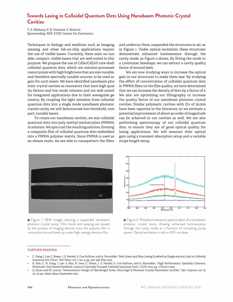
and undercut them, suspended the structures in air, as in Figure 1. Under optical excitation, these structures demonstrate enhanced luminescence through the cavity mode, as Figure 2 shows. By fitting the mode to a Lorentzian lineshape, we can extract a cavity quality factor of around 3000.
We are now studying ways to increase the optical gain in our structures to make them lase. By studying the effect of concentration of colloidal quantum dots in PMMA films on the film quality, we have determined that we can increase the density of dots by a factor of 5. We also are optimizing our lithography to increase the quality factor of our nanobeam photonic crystal cavities. Similar polymeric cavities with Q’s of 36,000 have been reported in the literature, so we estimate a potential improvement of about an order of magnitude can be achieved in our cavities as well. We are also performing spectroscopy of our colloidal quantum dots, to ensure they are of good optical quality for lasing applications. We will measure their optical gain using a transient absorption setup and a variable stripe length setup.
580 585 590 595 600 605 610 615 620 6250
50
100
150
200
250
300
350
Wavelength (nm)
Inte
nsity
(A.U
.)
Increasing Pump Power
Figure 1: SEM images showing a suspended nanobeam photonic crystal cavity. Film cracks and warping are caused by the process of imaging devices since the polymer film is nonconductive and heats up under high-energy electron flux.
Figure 2: Photoluminescence spectra taken of a nanobeam photonic crystal cavity showing enhanced luminescence through the cavity mode as a function of increasing pump power. Optical excitation is with a 400-nm laser.
FURTHER READING
• C. Dang, J. Lee, C. Breen, J. S. Steckel, S. Coe-Sullivan, and A. Nurmikko, “Red, Green and Blue Lasing Enabled by Single-exciton Gain in Colloidal Quantum Dot Films,” Nat Nano, vol. 7, no. 5, pp. 335–339, May 2012.
• K. Roh, C. H. Dang, J. Lee, S. Ahn, H. Jeon, C. Breen, J. S. Steckel, S. Coe-Sullivan, and A. Nurmikko, “High Performance, Spatially Coherent, Multicolor Distributed Feedback Lasers in Optically Pumped Colloidal Quantum Dots,” CLEO: 2013, pp. CTh4G.7, 2013.
• Q. Quan and M. Loncar, “Deterministic Design of Wavelength Scale, Ultra-high Q Photonic Crystal Nanobeam Cavities,” Opt. Express, vol. 19, no. 19, pp. 18529–18542, September 2011.