Embed Size (px)
Citation preview
PHOTONIC SYNTHESIS AND HARDWARE CORRELATIONS OF
ULTRABROADBAND RADIO-FREQUENCY WAVEFORMS AND POWER
SPECTRA VIA OPTICAL PULSE SHAPING
A Dissertation
Submitted to the Faculty
of
Purdue University
by
Ingrid Shihting Lin
In Partial Fulfillment of the
Requirements for the Degree
of
Doctor of Philosophy
August 2008
Purdue University
West Lafayette, Indiana
ii
This thesis is dedicated to my Father Tsing-Fa Lin who taught me the beauty of knowledge
iii
ACKNOWLEDGEMENT
Special thanks to Prof. A.M. Weiner who provides the best research guidance and most patience throughout my direct Ph. D study at Purdue. This research work would not be possible without his advices and support. I also like to thank the group members in Ultrafast Optics and Optical Fiber Communication Laboratory, especially Jason McKinney, Dan Leaird, Zhi Jiang and F.S. Toong. Many thanks to Hsiao-Kuan Yuan and my other friends from Purdue who always love and support me under any circumstances over these years. Finally, I sincerely appreciate the sponsorship from U.S. Department of Education for a three year fellowship of Graduate Assistance in Areas of National Need (GAANN) during my study at Purdue from 2003-2006.
iv
TABLE OF CONTENTS Page LIST OF TABLES......................................................................................................vi LIST OF FIGURES ...................................................................................................vii LIST OF ABBREVIATIONS...................................................................................xiii ABSTRACT............................................................................................................... xv 1. INTRODUCTION .............................................................................................. 1 2. PHOTONIC SYNTHESIS OF ARBITRARY RF WAVEFORMS AND INTRODUCTION TO ULTRAWIDE BANDWIDTH COMMUNICATION.4 2.1 Fourier-Transform Pulse Shaping................................................. 5 2.1.1 Transmissive Geometry FT Pulse Shaper...................... 5 2.1.2 Reflective Geometry FT Pulse Shaper........................... 5 2.1.3 Discussion on Practical Design and Calibration............ 6 2.2 Arbitrary Waveform Generation................................................... 7 2.2.1 Experimental apparatus.................................................. 8 2.2.2 Direct Mapping from Wavelength to Time ................... 9 2.3 Bandwidth Engineering Concept ................................................ 10 2.4 Ultra-Wide Bandwidth Communication ..................................... 10 2.4.1 Introduction to Ultra-Wide Bandwidth Impulse Radio ............................................................................ 10 2.4.2 UWB Impulse Radio Signaling and Modulation ......... 14 3. MEASUREMENTS AND RESULTS.............................................................. 16 3.1 Arbitrary Waveform Generation................................................. 16 3.1.1 Sinusoidal RF Waveforms ........................................... 16 3.1.2 Broadband RF Waveforms .......................................... 18 3.1.3 Equalized RF Waveforms ............................................ 23 3.2 Power Spectra Design and Generation ....................................... 25 3.2.1 Modified Gerchberg-Saxton Algorithm....................... 25 3.2.2 Optimized Spectrum Generation.................................. 27
v
Page
3.3 UWB Spectrum Generation ........................................................ 31 4. CORRELATION DETECTION PROCESS THEORY ................................... 32
4.1 Correlation Detection Experiment configurations...................... 32 4.1.1 Introduction to Mixers ................................................. 32 4.1.2 AWG Transmitter and Heterodyne Receiver............... 35
4.1.3 Characterization of Correlation system- Orthonormal signals..................................................... 36 4.2 Concept of UWB-CDMA Transmission and detection .............. 39
5. EXPERIMENTAL MEASUREMENTS OF ULTRA-WIDEBAND CORRELATION DETECTION PROCESS.................................................... 43
5.1 Hardware Correlation Detection of Ultra-wideband RF Signals Generated via Optical Pulse Shaping......................................... 44
5.1.1 Mixer-based Ultra-wideband Correlator Apparatus .... 45 5.1.2 Correlation Measurements over RF cable ................... 46 5.2 Correlation Detection over Wireless link ................................... 57 5.2.1 Antenna Overview, Simulations, and Frequency Responses..................................................................... 58 5.2.2 Dispersion Pre-compensation of Broadband Waveforms................................................................... 62 5.2.3 Wireless Correlation Measurements ............................ 64 5.3 Discussion of Waveform dc Pedestal Removal .......................... 67 6. CONCLUSIONS............................................................................................... 71 LIST OF REFERENCES........................................................................................... 73 APPENDICES A Modified Gerchberg-Saxtan Algorithm............................................................ 79 B Analysis of Horn Antenna................................................................................. 83 C Design of Ultrawideband High-Passed filter .................................................... 89 D Commercial Progress on Electronic based UWB System ................................ 93 VITA.......................................................................................................................... 97

vi
LIST OF TABLES Table Page 2.1 Average Emission Limits Applicable to UWB Operation.............................. 12 A.1 Parameters of Matlab optimization options ................................................... 81
vii
LIST OF FIGURES Figure Page 2.1 Schematic of femtosecond pulse shaping ......................................................... 4 2.2 Transmissive geometry Fourier-Transform pulse shaper ................................. 5 2.3 Reflective geometry Fourier-Transform pulse shaper ...................................... 6 2.4 Apparatus for arbitrary waveform Generation.................................................. 8 2.5 Wall chart of United-State frequency allocation (3 GHz to 6.42 GHz) ......... 11 2.6 UWB power emission limits ........................................................................... 12 2.7 Schematic of UWB transmission .................................................................... 13 2.8 Example of AIRMA modulation scheme ....................................................... 14 2.9 Example of DIRMA modulation scheme, 1bit/symbol .................................. 15 2.10 Example of DIRMA modulation scheme, 3bits/symbol ............................... 15 3.1 (a) Sinusoidal patterned optical spectrum (b) Sinusoidal RF waveform........ 16 3.2 (a) Sinusoidal patterned optical spectrum (b) Sinusoidal RF (2.5 GHz) (c) RF power spectrum.......................................................................................... 17 3.3 Frequency modulated (a) optical spectrum (b) RF waveform (1.25/2.5/5 GHz) (c) RF power spectrum................................................................................... 18 3.4 (a) UWB monocycles RF waveform (b) RF power spectrum ........................ 19 3.5 (a) Impulsive RF waveform with (b) super-Gaussian target RF spectrum..... 20 3.6 Simulated chirped spectrum with different chirp parameters ......................... 21 3.7 Simulated chirped waveform for C = 1.5e-19 ................................................ 22
viii
Figure Page 3.8 (a) Chirped waveform for C = 1.5e-19 (b) RF power spectrum ..................... 23 3.9 Equalized sinusoidal (a) optical spectrum (b) temporal waveform ................ 24 3.10 Modified Gerchberg-Saxton algorithm ......................................................... 25 3.11 (a) direct-specified design with apodization (b) optimized spectrum design26 3.12 (a) bandpass spectrum and its (b) associated temporal waveform................ 28 3.13 (a) bandstop spectrum and its (b) associated temporal waveform................ 29 3.14 (a) upstairs spectrum and its (b) associated temporal waveform.................. 30 3.15 (a) downstairs spectrum and its (b) associated temporal waveform............. 31 3.16 (a) UWB 3.1-10.6 flat spectrum and its (b) associated temporal waveform 31 4.1 mixer operation: down-conversion ................................................................. 33 4.2 mixer operation: up-conversion ...................................................................... 33 4.3 AWG transmitter apparatus ............................................................................ 35 4.4 Heterodyne receiver apparatus........................................................................ 36 4.5 AWG transmitter with orthonormal transmitted signal Wtr(t) ....................... 38 4.6 Heterodyne receiver with orthonormal template {Wn(t)}.............................. 39 4.7 Concept of spread-time CDMA transmitted signal generation ...................... 40 4.8 Concept of spread-time CDMA receiver ........................................................ 40 4.9 Generation of transmitted signal of UWB spread-time CDMA with PAM modulation scheme ........................................................................................ 40 4.10 Generation of transmitted signal of UWB spread-time/time-hopping CDMA with PPM modulation scheme ....................................................................... 41 5.1 Conceptual illustration of RF mixer-based UWB correlator .......................... 44
ix
Figure Page 5.2 Setup of photonic processing UWB RF correlator with optical pulse shapers and optical tunable delay line ........................................................................ 46 5.3 M-sequence of 7 bits (a) generated RF waveforms, solid: shaper #1 dashed: shaper #2; (b) correlation measurement......................................................... 47 5.4 Uniform distributed random sequence (a) Generated RF waveforms, solid : sequence #1 from shaper #1, dash: sequence #1 from shaper #2 (b) solid : sequence #2 from shaper #1, dash: sequence #2 from shaper #2; (c) Correlation traces of random sequence, solid: autocorrelation with sequence #1, dash: crosscorrelation between sequence #1 and #2 (d) solid: autocorrelation with sequence #2, dash: cross-correlation between sequence #1 and #2 ........................................................................................ 49 5.5 Ultrawideband impulsive signals (a) Generated RF waveforms, solid : shaper #1, dash: shaper #2 (b) RF power spectrum measurement; (c) Autocorrelation measurement (d) Simulated autocorrelation........................ 50 5.6 Measurement of (a) pixel-time mapping, blue circles: shaper #1, red line: shaper #1 - fitting, green circles: shaper #2, pink line: shaper #2 - fitting; (b) pixel-time deviation between fitted curve of shaper #1 and #2 pixel-time mapping.......................................................................................................... 51 5.7 Temporal waveforms of UWB linear chirped signals (a) WF1: down- chirped waveforms, inset: RF spectrum (b) WF2: up-chirped waveforms; Measured correlation traces (c) bold solid: matched WF1-WF1, dashed: un-matched: WF1-WF2, (d) bold solid: matched WF2-WF2, dashed: un- matched: WF2-WF1....................................................................................... 52 5.8 Simulation of linear chirped waveform correlation traces. WF1 denotes up-chirped signal, WF2 denotes down-chirped signal. (a) simulation using ideal waveforms - solid: matched WF1-1, dashed: un-matched WF1-2, (b) simulation using ideal waveforms - solid: matched WF2-2, dashed: un- matched WF2-1, (c) simulation using actual measured waveforms - solid: matched WF1-1, dashed: un-matched WF1-2, (d) simulation using actual measured waveforms - solid: matched WF2-2, dashed: un-matched WF2- 1...................................................................................................................... 53 5.9 Linear chirped scope traces of mixer output (a) solid: matched WF1-WF1, dashed: un-matched WF1-WF2 (b) solid: matched WF2-WF2, dashed: un- matched WF2-WF1........................................................................................ 55
x
Figure Page 5.10 Temporal waveforms of user-defined orthogonal signals (a) WF1: sequence #1 (b) WF2: sequence #2; Correlation traces (c) solid: matched WF1-WF1, dashed: un-matched WF1-WF2 (d) solid: matched WF2-WF2, dashed: un-matched WF2-WF1 ..................................................................... 56 5.11 Typical electromagnetic horn antenna configurations (a) E-plane (b) H- plane (c) Pyramidal (d) Conical..................................................................... 58 5.12 Picture of commercial UWB Horn antenna .................................................. 59 5.13 Simulations of commercial horn antenna in E-plane and H-plane ............... 59 5.14 Short pulse response measurement (a) transmitted pulse (b) received signal ............................................................................................................ 60 5.15 Frequency response via short pulse excitation in light of sight (a) horn pair (b) bowtie to horn ........................................................................................ 61 5.16 Liner chirped waveform (a) at transmitted antenna without highpass filter (b) at received antenna without highpass filter, late time ripples ~5 ns (c) at transmitted antenna with highpass filter (d) at received antenna with highpass filter, late time ripples ~2ns .......................................................... 62 5.17 Schematics of antenna link compensation .................................................... 63 5.18 Wireless transmission of linear chirped signals (a) antenna received signal (b) antenna received pre-compensated signal .............................................. 64 5.19 Ultra-wideband wireless correlation detection setup (a) RF Transmitter (b) Heterodyne receiver with local oscillator; Purple lines indicate RF cables, and black lines are optical fibers. The femtosecond pulses are produced from one fiber laser and sent into the same fiber stretcher (smf). The pulses are then split by a 3dB optical splitter prior to the pulse shapers ......................................................................................................... 64 5.20 Measurement of wireless correlation detection of linear chirped signals (a- b)without any waveform compensation, (c-d) with RF waveform pre- compensation. WF1 denotes up-chirped signal, WF2 denotes down- chirped signal ............................................................................................... 66 5.21 Measurement of wireless correlation detection of orthogonalized linear
xi
Figure Page chirped signals with RF waveform pre-compensation. WF1 denotes up- chirped signal, WF2 denotes down-chirped signal. (a) WF1-1 vs WF1-2 (b) WF2-2 vs WF2-1 ......................................................................................... 67 5.22 (left) Schematic of 3dB RF coupler operation (Right) Combination of RF coupler and inverting transformer................................................................ 68 5.23 (a) Sinusoidal signal prior to inverting transformer (b) Sinusoidal signal after inverting transformer ................................................................................... 68 5.24 Signal dc pedestal removal setup and associated waveforms....................... 69 5.25 Simulation of combination of RF coupler and inverting transformer .......... 70 A.1 Modified Gerchberg-Saxton algorithm.......................................................... 79 B.1 (a) Schematic of highpass constant-k filter section in π form with inductors and capacitor (b) schematic of associated ADS simulation........... 83 B.2 Schematic of ADS simulation with various component packages................. 84 B.3 Simulation results with various component packages ................................... 85 B.4 Measurements of fabricated highpassed filters with vector network analyzer (a) magnitude response of HPF #1 (b) phase response of HPF #1 (c) magnitude response of HPF #2 (d) phase response of HPF #2 ................ 85 B.5 Short pulse response measurement of fabricated highpassed filters (a) short pulse in time domain (b) RF power spectrum of associated short pulse (c) highpass-filtered short pulse in time domain (d) RF power spectrum of associated highpass filtered short pulse ..................................... 86 B.6 Picture of physical highpass filter implementation with SMA connectors ...................................................................................................... 87 B.7 Broadband linear chirped signal (a) temporal waveform prior to highpass filter (b) temporal waveform after highpass filtering (c) RF linear chirped spectrum prior to highpass filter (d) RF linear chirped spectrum after highpass filtering............................................................................................ 88 C.1 Pyramidal horn and coordinate system (a) pyramidal horn (b) E-plane
xii
Figure Page view (c) H-plane view.................................................................................... 91 C.2 Simulations of commercial horn antenna in E-plane and H-plane ................ 92 D.1 Freescale XS110 Ultrawideband solution system architecture...................... 94 D.2 The WiMCA specification allows multiple applications to coexist and share a single UWB radio platform (top) and its multiband frequency band plan (bottom).................................................................................................. 95
xiii
LIST OF ABBREVIATIONS A/D Analog-to-digital AIRMA Analog impulse radio multiple access AWG Arbitrary waveform generator BFSK Binary frequency shift keying BW Bandwidth CDMA Code division multiple access CFR Code of Federal Regulation DC Direct current DIRMA Digital impulse radio multiple access DST Direct space to time EDFA Erbium doped fiber amplifier EIRP Effective isotropic radiated power ER Extinction ratio FBG Fiber Bragg grating FCC Federal Communications Commission FT Fourier Transform GPR Ground penetrating radar GS Gram-Schmidts GS Gerchberg-Saxton HPF High passed filter IF Intermediate frequency IFT Inverse Fourier transform LCM Liquid crystal modulator LO Local oscillator LOS Light of sight LPD Low probability of detection LPF Low passed filter LPI Low probability of interception MA Multiple access MAC Media access control MB Multiband O/E optical-to-electrical OFDM Frequency division multiplexing OOK On off keying OSA Optical spectrum analyzer PAM Pulse amplitude modulation PBS Polarization beam splitter
xiv
PN Pseudorandom noise PPM Pulse position modulation PSK Phase shift keying PSD Power spectral density RF Radio Frequency SAW Surface acoustic wave SMA SubMiniature version A SMF Single mode fiber THSS Time hopping spread spectrum UWB Ultrawideband VNA Vector Network Analyzer
xv
ABSTRACT
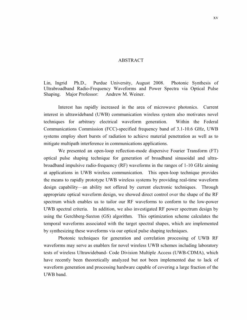
Lin, Ingrid Ph.D., Purdue University, August 2008. Photonic Synthesis of Ultrabroadband Radio-Frequency Waveforms and Power Spectra via Optical Pulse Shaping. Major Professor: Andrew M. Weiner.
Interest has rapidly increased in the area of microwave photonics. Current interest in ultrawideband (UWB) communication wireless system also motivates novel techniques for arbitrary electrical waveform generation. Within the Federal Communications Commission (FCC)-specified frequency band of 3.1-10.6 GHz, UWB systems employ short bursts of radiation to achieve material penetration as well as to mitigate multipath interference in communications applications.
We presented an open-loop reflection-mode dispersive Fourier Transform (FT) optical pulse shaping technique for generation of broadband sinusoidal and ultra-broadband impulsive radio-frequency (RF) waveforms in the ranges of 1-10 GHz aiming at applications in UWB wireless communication. This open-loop technique provides the means to rapidly prototype UWB wireless systems by providing real-time waveform design capability—an ability not offered by current electronic techniques. Through appropriate optical waveform design, we showed direct control over the shape of the RF spectrum which enables us to tailor our RF waveforms to conform to the low-power UWB spectral criteria. In addition, we also investigated RF power spectrum design by using the Gerchberg-Saxton (GS) algorithm. This optimization scheme calculates the temporal waveforms associated with the target spectral shapes, which are implemented by synthesizing these waveforms via our optical pulse shaping techniques.
Photonic techniques for generation and correlation processing of UWB RF waveforms may serve as enablers for novel wireless UWB schemes including laboratory tests of wireless Ultrawideband- Code Division Multiple Access (UWB-CDMA), which have recently been theoretically analyzed but not been implemented due to lack of waveform generation and processing hardware capable of covering a large fraction of the UWB band.
xvi
To illustrate the capability of ultrawideband correlation detection, we demonstrate hardware auto/cross- correlation measurements of photonically generated ultrawideband RF burst waveforms in the 3-10 GHz range. Full delay dependent correlation studies with matched waveform pairs reveal correlation peaks ~ 15dB above those obtained with non-matching sets of waveforms. The possibility of real-time correlation detection is also explored, as are correlation measurements of waveforms that are transmitted over a short line-of-sight wireless link. With waveforms modified to precompensate for antenna dispersion, 7 dB correlation contrast between matched and non-matched waveform pairs is obtained. Our results suggest hardware correlation detection as a possibility for processing of arbitrary waveforms in an UWB receiver.
1
1. INTRODUCTION
Interest has rapidly increased in the area of microwave photonics—the realm
where optical and radio-frequency (RF) signals as well as operations are combined to increase RF system performance. Specifically, optical analog-to-digital (A/D) conversion [1], [2] and microwave-photonic links [3] have garnered significant research interest. The former has been demonstrated to enable 130 GS/s (Giga-sample per second) A/Ds [2] and the latter has found application in data transmission as well as remote local-oscillator operations [3]. Pulsed radar and high-frequency wireless systems applications have motivated substantial research in the area of photonic arbitrary waveform generation systems, where optical signals are used to generate arbitrary electrical waveforms. Pure narrowband microwave/millimeter electromagnetic signals have been generated (12.4 and 37.2 GHz) through heterodyning different longitudinal modes of a modelocked semiconductor laser [4].
Current interest in ultrawideband (UWB) wireless systems for communications [5], ground penetrating radar (GPR), and imaging systems also motivates novel techniques for arbitrary electrical waveform generation. Within the Federal Communications Commission specified frequency band of 3.1–10.6 GHz, UWB systems employ short bursts [6] of radiation to achieve material penetration (imaging, GPR) as well as to mitigate multipath interference in communications applications.
In the previous work in our group, we used optical pulse sequences from a direct space-to time (DST) pulse shaper to generate mm-wave arbitrary waveforms in the > 15 GHz range [7]. Another group [8] has previously demonstrated the use of a Fourier Transform (FT) shaper and dispersive stretcher for arbitrary waveform generation (AWG) in range below 10 GHz. Their work used a computer-learning algorithm to iteratively modify the pulse shaper settings until the desired microwave waveform was obtained. The FT pulse shaper fundamentally has a lower optical loss of ~ 5dB. In addition, a few groups work on the fiber Bragg gratings (FBG) as spectral shaping elements for UWB waveform generation by tuning two FBG-based variable optical filters [9-10].
2
Here, we demonstrate the first open-loop reflective geometry Fourier Transform (FT) pulse shaper for generation of RF waveforms at center frequencies of 1-10 GHz. By using a more efficient open-loop control approach, we are capable of generating arbitrary waveforms immediately (without iteration) once we apply the masking pattern onto the programmable liquid crystal modulator (LCM). This is made possible through careful characterization studies, which give us precise knowledge of the phase delay of the stretcher and the optical spectral response laws for our shaper. In addition to more rapid waveform generation, the design of our reflective FT pulse shaper demonstrates lower insertion loss (~ 5 dB) than the transmissive FT pulse shaper (~ 8 dB). In this work, our FT pulse shaping technique generates broadband sinusoidal and ultra-broadband impulsive RF waveforms [11] aimed at applications in UWB wireless communication. In addition to the extremely flat RF power spectra that fill the UWB band we obtained via impulsive RF time-domain waveforms [12-13], we also exploit an optimization approach with RF spectral phase as a variable and demonstrate innovative flat RF power spectra in the UWB frequency band via arbitrarily shaped RF waveforms [14].
We have reported studies demonstrating the use of optical pulse shaping followed by optical-to-electrical conversion for generation of arbitrary burst electrical waveforms with instantaneous bandwidths (BW) spanning (or in some cases significantly exceeding) the UWB frequency band (3.1 – 10.6 GHz). Recently commercial electronic arbitrary waveform technology has also advanced to > 5 GHz instantaneous bandwidth [15], which is sufficient, if appropriately upconverted, to cover much of the UWB band. Optical techniques retain advantages such as possibility of reaching much higher instantaneous bandwidth and compatibility with remoting applications. The advent of UWB arbitrary waveform generation, using either photonic or electronic solutions, allows new capabilities, such as antenna dispersion precompensation, to be applied on the transmitter end for UWB wireless studies [16]. However, to fully exploit arbitrary RF waveforms for UWB, new processing approaches are needed at the receiver, since conventional analog-to-digital conversion and digital signal processing are inadequate to handle the full UWB band.
We demonstrate hardware auto/cross-correlation measurements of photonically generated ultrawideband (UWB) RF burst waveforms in the 3-10 GHz range. Full delay dependent correlation studies with matched waveform pairs reveal correlation peaks ~ 15 dB above those obtained with non-matching sets of waveforms. The possibility of real-time correlation detection is also explored, as are correlation
3
measurements of waveforms that are transmitted over a short line-of-sight wireless link. With waveforms modified to precompensate for antenna dispersion, 7 dB correlation contrast between matched and non-matched waveform pairs is obtained. Our results suggest novel photonics enabled hardware correlation detection as a possibility for processing of arbitrary waveforms in an Ultra-wideband (UWB) receiver.
The remainder of this thesis is structured as follows. In chapter 2, the technology of Fourier Transform optical pulse shaping and arbitrary waveform generation techniques are elaborated. The concept of the bandwidth engineering and ultrawide bandwidth communication is also introduced. Chapter 3 presents the experimental results of RF waveform and power spectra generation. In chapter 4, we elaborate the correlation detection process theory. Chapter 5 demonstrates the hardware correlation detection experimental measurements and associated discussions. Chapter 6 concludes our work.
4
2. PHOTONIC SYNTHESIS OF ARBITRARY RF WAVEFORMS AND INTRODUCTION TO ULTRAWIDE BANDWIDTH
COMMUNICATION
The femtosecond optical pulse shaping [17] is now a well established technology
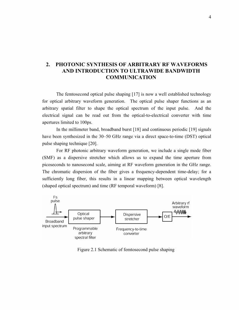
for optical arbitrary waveform generation. The optical pulse shaper functions as an arbitrary spatial filter to shape the optical spectrum of the input pulse. And the electrical signal can be read out from the optical-to-electrical converter with time apertures limited to 100ps.
In the millimeter band, broadband burst [18] and continuous periodic [19] signals have been synthesized in the 30–50 GHz range via a direct space-to-time (DST) optical pulse shaping technique [20].
For RF photonic arbitrary waveform generation, we include a single mode fiber (SMF) as a dispersive stretcher which allows us to expand the time aperture from picoseconds to nanosecond scale, aiming at RF waveform generation in the GHz range. The chromatic dispersion of the fiber gives a frequency-dependent time-delay; for a sufficiently long fiber, this results in a linear mapping between optical wavelength (shaped optical spectrum) and time (RF temporal waveform) [8].
Figure 2.1 Schematic of femtosecond pulse shaping
5
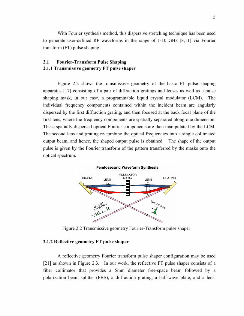
With Fourier synthesis method, this dispersive stretching technique has been used to generate user-defined RF waveforms in the range of 1-10 GHz [8,11] via Fourier transform (FT) pulse shaping. 2.1 Fourier-Transform Pulse Shaping 2.1.1 Transmissive geometry FT pulse shaper
Figure 2.2 shows the transmissive geometry of the basic FT pulse shaping apparatus [17] consisting of a pair of diffraction gratings and lenses as well as a pulse shaping mask, in our case, a programmable liquid crystal modulator (LCM). The individual frequency components contained within the incident beam are angularly dispersed by the first diffraction grating, and then focused at the back focal plane of the first lens, where the frequency components are spatially separated along one dimension. These spatially dispersed optical Fourier components are then manipulated by the LCM. The second lens and grating re-combine the optical frequencies into a single collimated output beam, and hence, the shaped output pulse is obtained. The shape of the output pulse is given by the Fourier transform of the pattern transferred by the masks onto the optical spectrum.
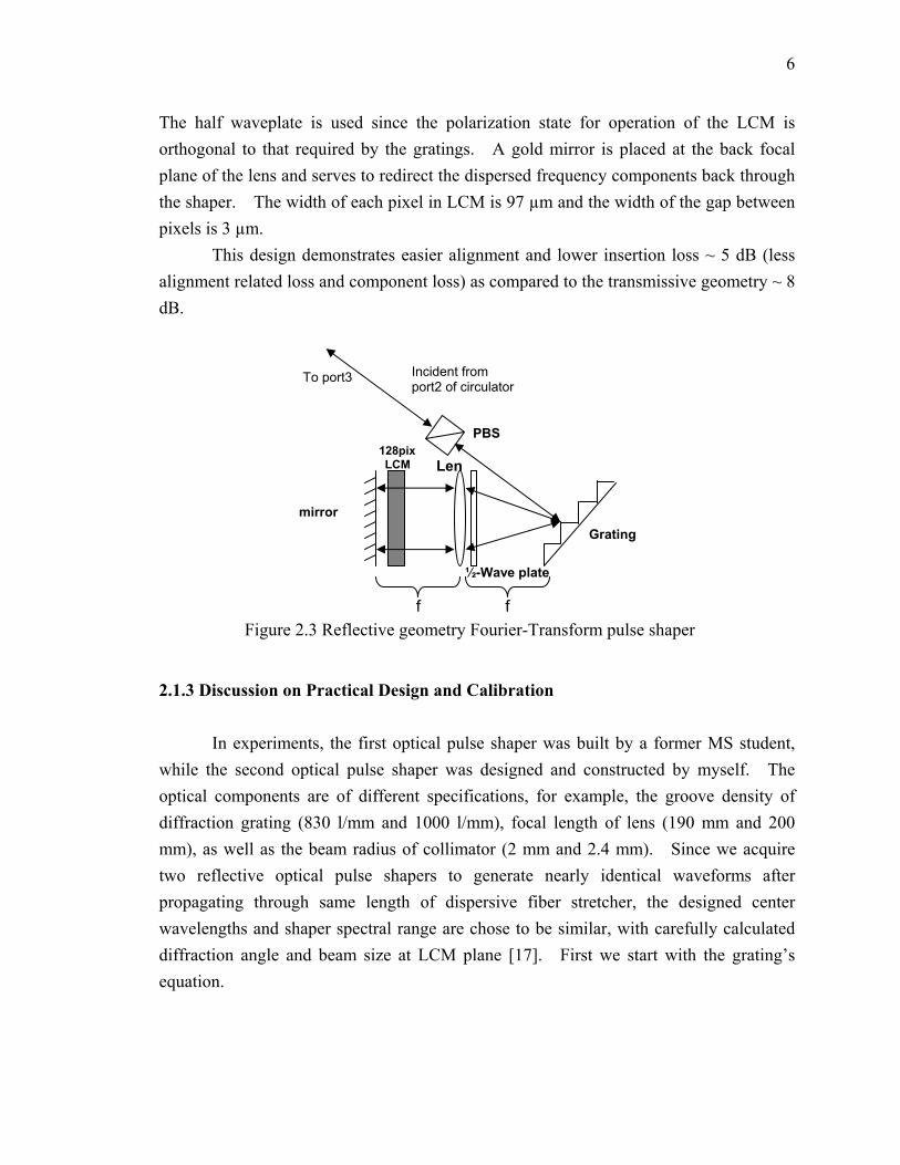
2.1.2 Reflective geometry FT pulse shaper
A reflective geometry Fourier transform pulse shaper configuration may be used [21] as shown in Figure 2.3. In our work, the reflective FT pulse shaper consists of a fiber collimator that provides a 5mm diameter free-space beam followed by a polarization beam splitter (PBS), a diffraction grating, a half-wave plate, and a lens.
Figure 2.2 Transmissive geometry Fourier-Transform pulse shaper
6
The half waveplate is used since the polarization state for operation of the LCM is orthogonal to that required by the gratings. A gold mirror is placed at the back focal plane of the lens and serves to redirect the dispersed frequency components back through the shaper. The width of each pixel in LCM is 97 µm and the width of the gap between pixels is 3 µm.
This design demonstrates easier alignment and lower insertion loss ~ 5 dB (less alignment related loss and component loss) as compared to the transmissive geometry ~ 8 dB.
2.1.3 Discussion on Practical Design and Calibration In experiments, the first optical pulse shaper was built by a former MS student,
while the second optical pulse shaper was designed and constructed by myself. The optical components are of different specifications, for example, the groove density of diffraction grating (830 l/mm and 1000 l/mm), focal length of lens (190 mm and 200 mm), as well as the beam radius of collimator (2 mm and 2.4 mm). Since we acquire two reflective optical pulse shapers to generate nearly identical waveforms after propagating through same length of dispersive fiber stretcher, the designed center wavelengths and shaper spectral range are chose to be similar, with carefully calculated diffraction angle and beam size at LCM plane [17]. First we start with the grating’s equation.
f f
mirror
128pix LCM Len
½-Wave plate
Grating
PBS
Incident from port2 of circulator
To port3
Figure 2.3 Reflective geometry Fourier-Transform pulse shaper
7
λθθ md di =+ )sin(sin (2.1)
where d is grating constant, di θθ , are grating incident and diffraction angle, λ is
wavelength and m is diffraction order (in our case, m is taken as -1). Once we specified a certain incident angle (recommended to be less than 70 degrees), diffraction order, and the center wavelength, we could obtain the diffraction angle value for the center wavelength. Then, the spectral range can be derived as
cos ddx f
θλ∆=
∆ (2.2)
where f is lens focal length, is spectral range and x is LCM pixel aperture. For our LCM, x = 12.8mm. The beam size at the LCM plane can be calculated from the following,
0coscos
i
i d
fwwλ θπ θ
=
(2.3)
where wi is collimator beam radius. For convenience, we define the beam diameter at LCM layer as resolution (2w0), assuming difference of the beam diameter between focal plane and LCM layer is neglected. As the LCM layer and reflective mirror cannot be placed in the same plane at lens back focal plane, the beam diameter at LCM layer is usually larger than the calculated value and resulting in a degraded resolution. In the current optical pulse shapers for this thesis, the resolution is ~180µm (or, 2-pixel resolution), using old type of CRI LCM. For new type of LCM, where the LCM layers are placed at one surface of the apparatus and positioned closer to the reflective mirror, can achieve an one-pixel resolution. Also there is a trade-off between high resolution and low loss.
For carefully calibrating an optical pulse shaper, a polarizer is used to avoid polarization fluctuation. A beam splitter separates reference and signal path, where the reference beam is detected by a photodiode to monitor input power fluctuation while the signal beam is sent through a testing pixel of the LCM and reflected back by mirror, then detected by another photodetector. Both reference and signal are recorded via two lock-in amplifiers. When we obtain this calibration curve, one very important point here is that be sure to use the exact look-up mapping from the measured curve, instead of fitting
8
it with linear approximation. This would serve as an essential key to accurately control the LCM and thus generate precise user-defined waveforms. 2.2 Arbitrary Waveform Generation 2.2.1 Experimental apparatus
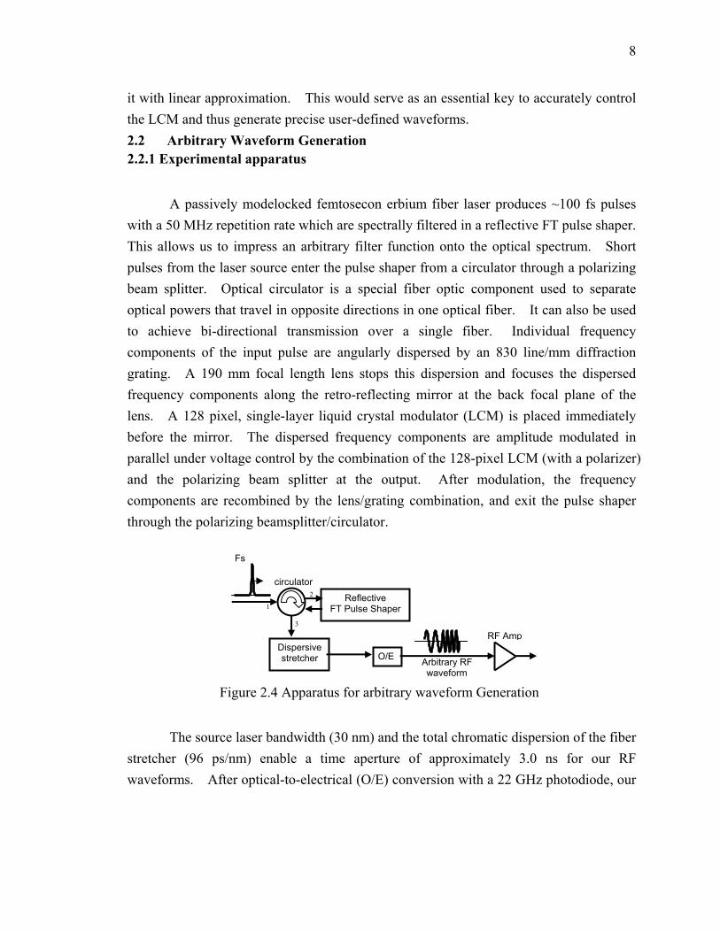
A passively modelocked femtosecon erbium fiber laser produces ~100 fs pulses
with a 50 MHz repetition rate which are spectrally filtered in a reflective FT pulse shaper. This allows us to impress an arbitrary filter function onto the optical spectrum. Short pulses from the laser source enter the pulse shaper from a circulator through a polarizing beam splitter. Optical circulator is a special fiber optic component used to separate optical powers that travel in opposite directions in one optical fiber. It can also be used to achieve bi-directional transmission over a single fiber. Individual frequency components of the input pulse are angularly dispersed by an 830 line/mm diffraction grating. A 190 mm focal length lens stops this dispersion and focuses the dispersed frequency components along the retro-reflecting mirror at the back focal plane of the lens. A 128 pixel, single-layer liquid crystal modulator (LCM) is placed immediately before the mirror. The dispersed frequency components are amplitude modulated in parallel under voltage control by the combination of the 128-pixel LCM (with a polarizer) and the polarizing beam splitter at the output. After modulation, the frequency components are recombined by the lens/grating combination, and exit the pulse shaper through the polarizing beamsplitter/circulator.
The source laser bandwidth (30 nm) and the total chromatic dispersion of the fiber
stretcher (96 ps/nm) enable a time aperture of approximately 3.0 ns for our RF waveforms. After optical-to-electrical (O/E) conversion with a 22 GHz photodiode, our
Reflective FT Pulse Shaper
Dispersive stretcher O/E
1
3
circulator 2
Fs
Arbitrary RF waveform
RF Amp
Figure 2.4 Apparatus for arbitrary waveform Generation
9
temporal RF waveforms are measured with a 50 GHz sampling oscilloscope and the RF spectra of these waveforms are measured with a 50 GHz RF spectrum analyzer.
Our pulse shaper operates in amplitude-modulation mode. The spectral pattern applied to the LCM is mapped directly to time by the 5.5km single mode fiber (SMF) stretcher. By manipulating the masking pattern of the LCM, we directly modulate the optical spectrum and, hence, the time-domain optical and electrical waveforms after the stretcher. The key difference between our work and previous demonstrations of this technique [8] is that our system operates in an open-loop configuration. Thorough characterization of our pulse shaper and dispersive stretcher enable real-time arbitrary RF waveform realization, without the need for iteration. 2.2.2 Direct Mapping from Wavelength to Time
We use a 5.5km Corning SMF-28 single mode fiber with dispersion parameter D = 17 ps/nm/km as a dispersive stretcher. We exploit this dispersive nature of the optical fibers to stretch the optical pulses. A dispersive system adds spectral phase ψ(ω) to the input short pulse. The output pulse is given by [22],
∫= )()(21 ωψωωωπ
jtjinout eeEde
(2.4)
where ein(t) is the input pulse with spectrum Ein(ω). In term of Taylor series expression, the spectral phase ψ(ω) comes from the dispersive system can be written as
...)(61)(
21)()()( 3
03
32
02
2
00 +−∂∂
+−∂∂
+−∂∂
+= ωωωψωω
ωψωω
ωψωψωψ
(2.5)
By looking at the concept of group velocity using Fourier transform identities, the Fourier transform of a delayed pulse a(t-τ) is given by A(ω)e-jωτ, therefore the frequency-dependent delay is
ωωψωτ
∂∂
−=)()(
(2.6)
10
In our experiment, when the pulses are extremely dispersed by 5.5km of single mode fiber, the quadratic spectral phase dominates the higher order Taylor series terms which leads to linear variation in delay with frequency. This allows us to have the direct wavelength-to-time mapping. As a result, lower frequency components will emerge first. Thus the desired optical waveform can be obtained by passing an optical pulse through the optical fiber to produce a stretched pulse with its optical spectrum shaped to the desired shape by the LCM.
The time aperture of the waveform ∆τ is related to the length of optical fiber L, the optical bandwidth ∆λ and the dispersion parameter D by
LD ⋅∆⋅=∆ λτ (2.7)
In our case, the time aperture ∆τ ≈ 3.27ns = 17(ps/nm/km)·35(nm)·5.5(km). 2.3 Bandwidth Engineering Concept
With careful waveform design, we can further tailor the RF spectrum of the
signals or generate very broadband signals which conform to the power emission limits of UWB and other communication applications. The associated waveforms can then be synthesized via the pulse shaping technique mentioned above. This enables the possibility of arbitrary RF power spectra generation as well. More details of spectrum design and generation results can be found in Section 3.2 and 3.3. 2.4 Ultra-Wide Bandwidth Communication 2.4.1 Introduction to Ultra-Wide Bandwidth Impulse Radio
The concept of Ultra-Wide Bandwidth (UWB) communication system was
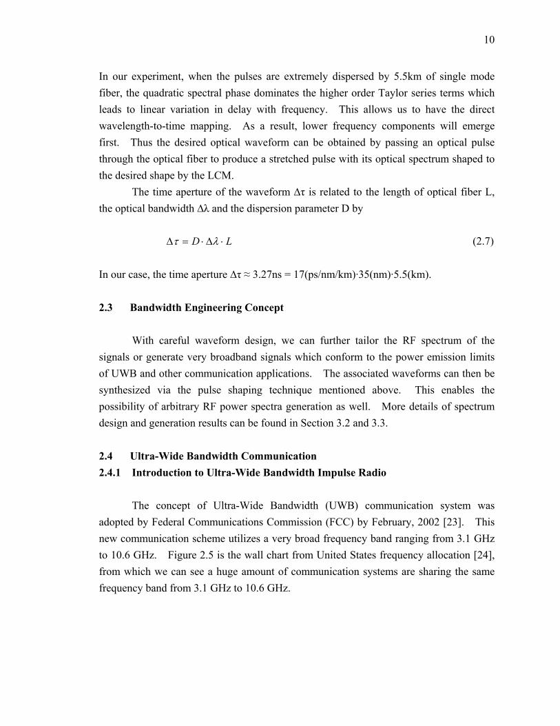
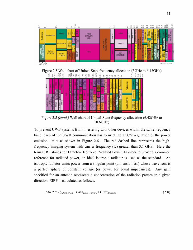
adopted by Federal Communications Commission (FCC) by February, 2002 [23]. This new communication scheme utilizes a very broad frequency band ranging from 3.1 GHz to 10.6 GHz. Figure 2.5 is the wall chart from United States frequency allocation [24], from which we can see a huge amount of communication systems are sharing the same frequency band from 3.1 GHz to 10.6 GHz.
11
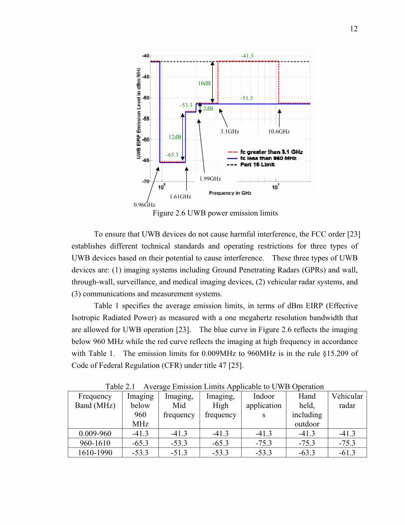
To prevent UWB systems from interfering with other devices within the same frequency band, each of the UWB communication has to meet the FCC’s regulation of the power emission limits as shown in Figure 2.6. The red dashed line represents the high-frequency imaging system with carrier-frequency (fc) greater than 3.1 GHz. Here the term EIRP stands for Effective Isotropic Radiated Power. In order to provide a common reference for radiated power, an ideal isotropic radiator is used as the standard. An isotropic radiator emits power from a singular point (dimensionless) whose wavefront is a perfect sphere of constant voltage (or power for equal impedances). Any gain specified for an antenna represents a concentration of the radiation pattern in a given direction. EIRP is calculated as follows, EIRP = Poutput of TX –LossTX to Antenna+GainAntenna . (2.8)
Figure 2.5 Wall chart of United-State frequency allocation (3GHz to 6.42GHz)
Figure 2.5 (conti.) Wall chart of United-State frequency allocation (6.42GHz to 10.6GHz)
12
To ensure that UWB devices do not cause harmful interference, the FCC order [23]
establishes different technical standards and operating restrictions for three types of UWB devices based on their potential to cause interference. These three types of UWB devices are: (1) imaging systems including Ground Penetrating Radars (GPRs) and wall, through-wall, surveillance, and medical imaging devices, (2) vehicular radar systems, and (3) communications and measurement systems.
Table 1 specifies the average emission limits, in terms of dBm EIRP (Effective Isotropic Radiated Power) as measured with a one megahertz resolution bandwidth that are allowed for UWB operation [23]. The blue curve in Figure 2.6 reflects the imaging below 960 MHz while the red curve reflects the imaging at high frequency in accordance with Table 1. The emission limits for 0.009MHz to 960MHz is in the rule §15.209 of Code of Federal Regulation (CFR) under title 47 [25].
Table 2.1 Average Emission Limits Applicable to UWB Operation Frequency
Band (MHz) Imaging below 960
MHz
Imaging, Mid
frequency
Imaging, High
frequency
Indoor application
s
Hand held,
including outdoor
Vehicular radar
0.009-960 -41.3 -41.3 -41.3 -41.3 -41.3 -41.3 960-1610 -65.3 -53.3 -65.3 -75.3 -75.3 -75.3 1610-1990 -53.3 -51.3 -53.3 -53.3 -63.3 -61.3
0.96GHz 1.61GHz
1.99GHz
3.1GHz 10.6GHz
-65.3
-53.3 -51.3
-41.3
10dB
12dB
2dB
Figure 2.6 UWB power emission limits
13
1990-3100 -51.3 -41.3 -51.3 -51.3 -61.3 -61.3 3100-10600 -51.3 -41.3 -41.3 -41.3 -41.3 -61.3 10600-22000 -51.3 -51.3 -51.3 -51.3 -61.3 -61.3 22000-29000 -51.3 -51.3 -51.3 -51.3 -61.3 -41.3 Above 29000 -51.3 -51.3 -51.3 -51.3 -61.3 -51.3
Mid-frequency imaging, consisting of through-wall imaging systems and surveillance systems, must operate with the –10 dB bandwidth within the frequency band 1990-10,600 MHz. High frequency imaging systems, equipment that will be operated exclusively indoors, and hand held UWB devices that may operate anywhere, including outdoors and for peer-to-peer applications, must operate with the –10 dB bandwidth within the frequency band 3100-10,600 MHz. All other imaging systems must operate with the –10 dB bandwidth below 960 MHz. Definition of UWB can also be expressed as that the ratio of the bandwidth to the center frequency is greater than 0.25.
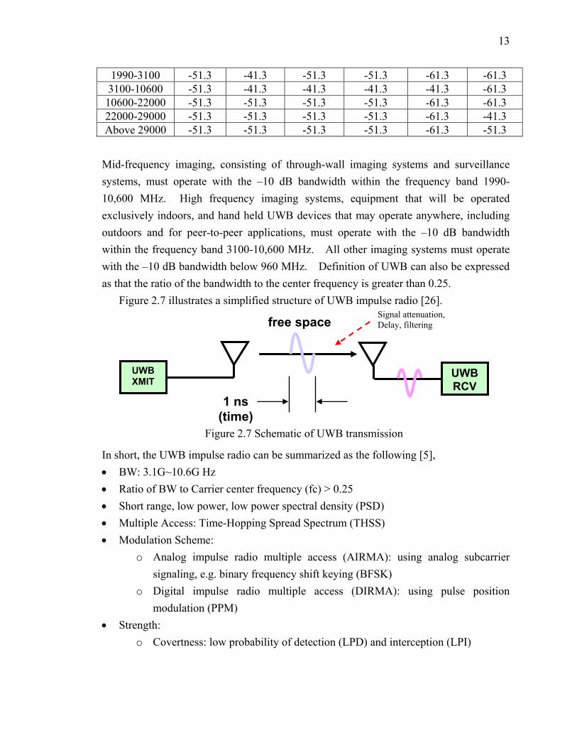
Figure 2.7 illustrates a simplified structure of UWB impulse radio [26].
In short, the UWB impulse radio can be summarized as the following [5], • BW: 3.1G~10.6G Hz • Ratio of BW to Carrier center frequency (fc) > 0.25 • Short range, low power, low power spectral density (PSD) • Multiple Access: Time-Hopping Spread Spectrum (THSS) • Modulation Scheme:
o Analog impulse radio multiple access (AIRMA): using analog subcarrier signaling, e.g. binary frequency shift keying (BFSK)
o Digital impulse radio multiple access (DIRMA): using pulse position modulation (PPM)
• Strength: o Covertness: low probability of detection (LPD) and interception (LPI)
UWBRCV
UWB XMIT
1 ns (time)
free spaceSignal attenuation, Delay, filtering
Figure 2.7 Schematic of UWB transmission
14
o No need of carrier recovery o Fine time resolution
• Weakness: o Long acquisition time o Timing jitter
2.4.2 UWB Impulse Radio Signaling and Modulation
For UWB signal representation, here we use Wtr(t,u) to represent a transmitted
pulse for user u [5], then the kth transmitted signal can be written as (2.9)
where Tf is the uniform spacing time period, Cj(k)(u) is the time hopping sequence of
pulse shift pattern, and dj(k)(u) is the modulation scheme, e.g. in pulse position
modulation a ‘0’ means no additional time shift for the time shopping sequence while a ‘1’ means a δ additional time shift. Tf is divided into Nh slots with width Tc. The product of Cj
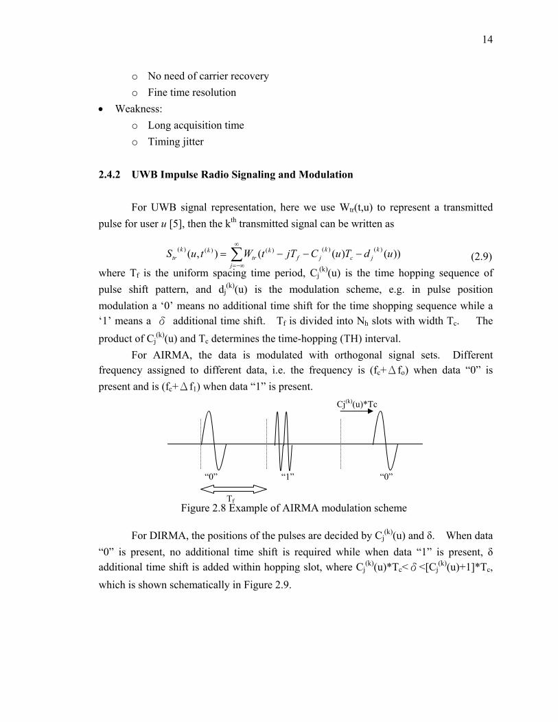
(k)(u) and Tc determines the time-hopping (TH) interval. For AIRMA, the data is modulated with orthogonal signal sets. Different
frequency assigned to different data, i.e. the frequency is (fc+Δfo) when data “0” is present and is (fc+Δf1) when data “1” is present.
For DIRMA, the positions of the pulses are decided by Cj
(k)(u) and δ. When data “0” is present, no additional time shift is required while when data “1” is present, δ additional time shift is added within hopping slot, where Cj
(k)(u)*Tc<δ<[Cj(k)(u)+1]*Tc,
which is shown schematically in Figure 2.9.
∑∞
−∞=
−−−=j
kjc
kjf
ktr
kktr udTuCjTtWtuS ))()((),( )()()()()(
Tf
Cj(k)(u)*Tc
“0” “1” “0”
Figure 2.8 Example of AIRMA modulation scheme
15
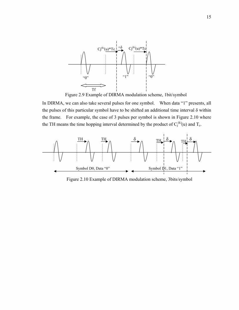
In DIRMA, we can also take several pulses for one symbol. When data “1” presents, all the pulses of this particular symbol have to be shifted an additional time interval δ within the frame. For example, the case of 3 pulses per symbol is shown in Figure 2.10 where the TH means the time hopping interval determined by the product of Cj
(k)(u) and Tc.
δ δ δ TH TH TH TH
Symbol D0, Data “0” Symbol D1, Data “1”
Tf
Cj(k)(u)*Tc
“0” “1” “0”
Cj(k)(u)*Tc +δ
Figure 2.9 Example of DIRMA modulation scheme, 1bit/symbol
Figure 2.10 Example of DIRMA modulation scheme, 3bits/symbol
16
3. MEASUREMENTS AND RESULTS
This chapter presents several representative waveforms generated in our system. In addition, the results of photonic synthesis of RF power spectra are also demonstrated.
3.1 Arbitrary Waveform Generation 3.1.1 Sinusoidal RF Waveforms
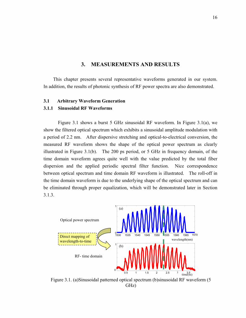
Figure 3.1 shows a burst 5 GHz sinusoidal RF waveform. In Figure 3.1(a), we
show the filtered optical spectrum which exhibits a sinusoidal amplitude modulation with a period of 2.2 nm. After dispersive stretching and optical-to-electrical conversion, the measured RF waveform shows the shape of the optical power spectrum as clearly illustrated in Figure 3.1(b). The 200 ps period, or 5 GHz in frequency domain, of the time domain waveform agrees quite well with the value predicted by the total fiber dispersion and the applied periodic spectral filter function. Nice correspondence between optical spectrum and time domain RF waveform is illustrated. The roll-off in the time domain waveform is due to the underlying shape of the optical spectrum and can be eliminated through proper equalization, which will be demonstrated later in Section 3.1.3.
1530 1535 1540 1545 1550 1555 1560 1565 0
1
wavelength(nm)
0.5 1 1.5 2 2.5 3 3.5 0
1
Optical power spectrum
RF- time domain
Direct mapping of wavelength-to-time
(a)
(b)
time(ns)
1570
Figure 3.1. (a)Sinusoidal patterned optical spectrum (b)sinusoidal RF waveform (5 GHz)
17
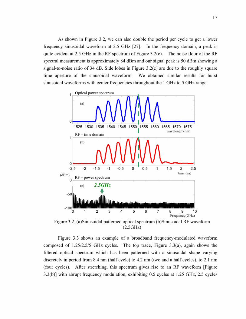
As shown in Figure 3.2, we can also double the period per cycle to get a lower
frequency sinusoidal waveform at 2.5 GHz [27]. In the frequency domain, a peak is quite evident at 2.5 GHz in the RF spectrum of Figure 3.2(c). The noise floor of the RF spectral measurement is approximately 84 dBm and our signal peak is 50 dBm showing a signal-to-noise ratio of 34 dB. Side lobes in Figure 3.2(c) are due to the roughly square time aperture of the sinusoidal waveform. We obtained similar results for burst sinusoidal waveforms with center frequencies throughout the 1 GHz to 5 GHz range.
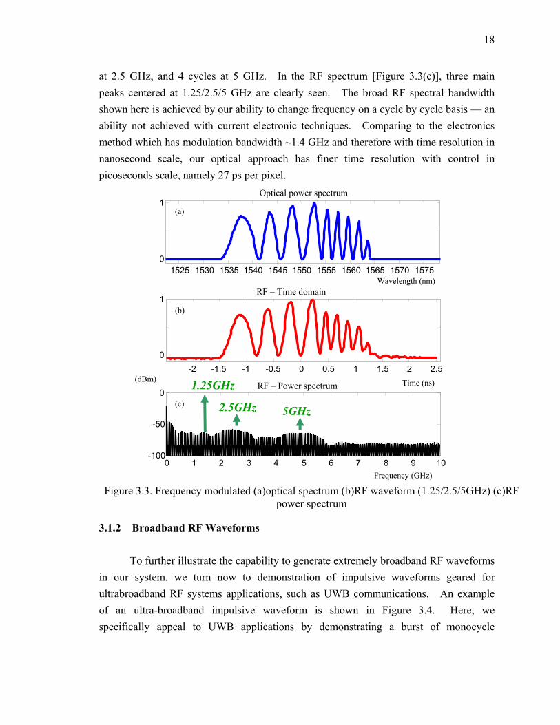
Figure 3.3 shows an example of a broadband frequency-modulated waveform
composed of 1.25/2.5/5 GHz cycles. The top trace, Figure 3.3(a), again shows the filtered optical spectrum which has been patterned with a sinusoidal shape varying discretely in period from 8.4 nm (half cycle) to 4.2 nm (two and a half cycles), to 2.1 nm (four cycles). After stretching, this spectrum gives rise to an RF waveform [Figure 3.3(b)] with abrupt frequency modulation, exhibiting 0.5 cycles at 1.25 GHz, 2.5 cycles
-2.5 -2 -1.5 -1 -0.5 0 0.5 1 1.5 2 2.5 0
1
1525 1530 1535 1540 1545 1550 1555 1560 1565 1570 1575 0
1
wavelength(nm)
time (ns)
0 1 2 3 4 5 6 7 8 9 10 -100
-50
0 (dBm)
2.5GHz
RF – time domain
RF – power spectrum
(a)
(b)
(c)
Optical power spectrum
Frequency(GHz)
Figure 3.2. (a)Sinusoidal patterned optical spectrum (b)Sinusoidal RF waveform (2.5GHz)
18
at 2.5 GHz, and 4 cycles at 5 GHz. In the RF spectrum [Figure 3.3(c)], three main peaks centered at 1.25/2.5/5 GHz are clearly seen. The broad RF spectral bandwidth shown here is achieved by our ability to change frequency on a cycle by cycle basis — an ability not achieved with current electronic techniques. Comparing to the electronics method which has modulation bandwidth ~1.4 GHz and therefore with time resolution in nanosecond scale, our optical approach has finer time resolution with control in picoseconds scale, namely 27 ps per pixel.
3.1.2 Broadband RF Waveforms To further illustrate the capability to generate extremely broadband RF waveforms
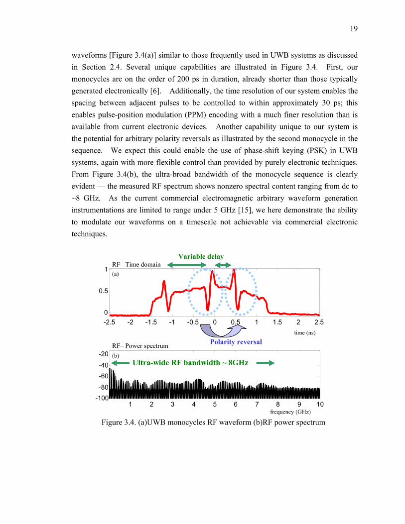
in our system, we turn now to demonstration of impulsive waveforms geared for ultrabroadband RF systems applications, such as UWB communications. An example of an ultra-broadband impulsive waveform is shown in Figure 3.4. Here, we specifically appeal to UWB applications by demonstrating a burst of monocycle
1525 1530 1535 1540 1545 1550 1555 1560 1565 1570 1575 0
1
0 1 2 3 4 5 6 7 8 9 10 -100
-50
0
Wavelength (nm)
Time (ns)
-2 -1.5 -1 -0.5 0 0.5 1 1.5 2 2.5 0
1
(dBm) 1.25GHz
2.5GHz 5GHz
RF – Time domain
RF – Power spectrum
Frequency (GHz)
(a)
(b)
(c)
Optical power spectrum
Figure 3.3. Frequency modulated (a)optical spectrum (b)RF waveform (1.25/2.5/5GHz) (c)RF power spectrum
19
waveforms [Figure 3.4(a)] similar to those frequently used in UWB systems as discussed in Section 2.4. Several unique capabilities are illustrated in Figure 3.4. First, our monocycles are on the order of 200 ps in duration, already shorter than those typically generated electronically [6]. Additionally, the time resolution of our system enables the spacing between adjacent pulses to be controlled to within approximately 30 ps; this enables pulse-position modulation (PPM) encoding with a much finer resolution than is available from current electronic devices. Another capability unique to our system is the potential for arbitrary polarity reversals as illustrated by the second monocycle in the sequence. We expect this could enable the use of phase-shift keying (PSK) in UWB systems, again with more flexible control than provided by purely electronic techniques. From Figure 3.4(b), the ultra-broad bandwidth of the monocycle sequence is clearly evident — the measured RF spectrum shows nonzero spectral content ranging from dc to ~8 GHz. As the current commercial electromagnetic arbitrary waveform generation instrumentations are limited to range under 5 GHz [15], we here demonstrate the ability to modulate our waveforms on a timescale not achievable via commercial electronic techniques.
1 2 3 4 5 6 7 8 9 10 -100 -80 -60 -40 -20
frequency (GHz)
Ultra-wide RF bandwidth ~ 8GHz
-2.5 -2 -1.5 -1 -0.5 0 0.5 1 1.5 2 2.5 0
0.5
1
time (ns)
Variable delay
Polarity reversal
RF– Time domain
RF– Power spectrum
(a)
(b)
Figure 3.4. (a)UWB monocycles RF waveform (b)RF power spectrum
20
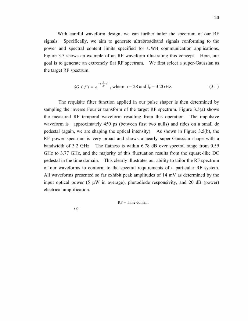
With careful waveform design, we can further tailor the spectrum of our RF signals. Specifically, we aim to generate ultrabroadband signals conforming to the power and spectral content limits specified for UWB communication applications. Figure 3.5 shows an example of an RF waveform illustrating this concept. Here, our goal is to generate an extremely flat RF spectrum. We first select a super-Gaussian as the target RF spectrum.
n
fpf
efSG)(
)(−
= , where n = 28 and fp = 3.2GHz. (3.1)
The requisite filter function applied in our pulse shaper is then determined by
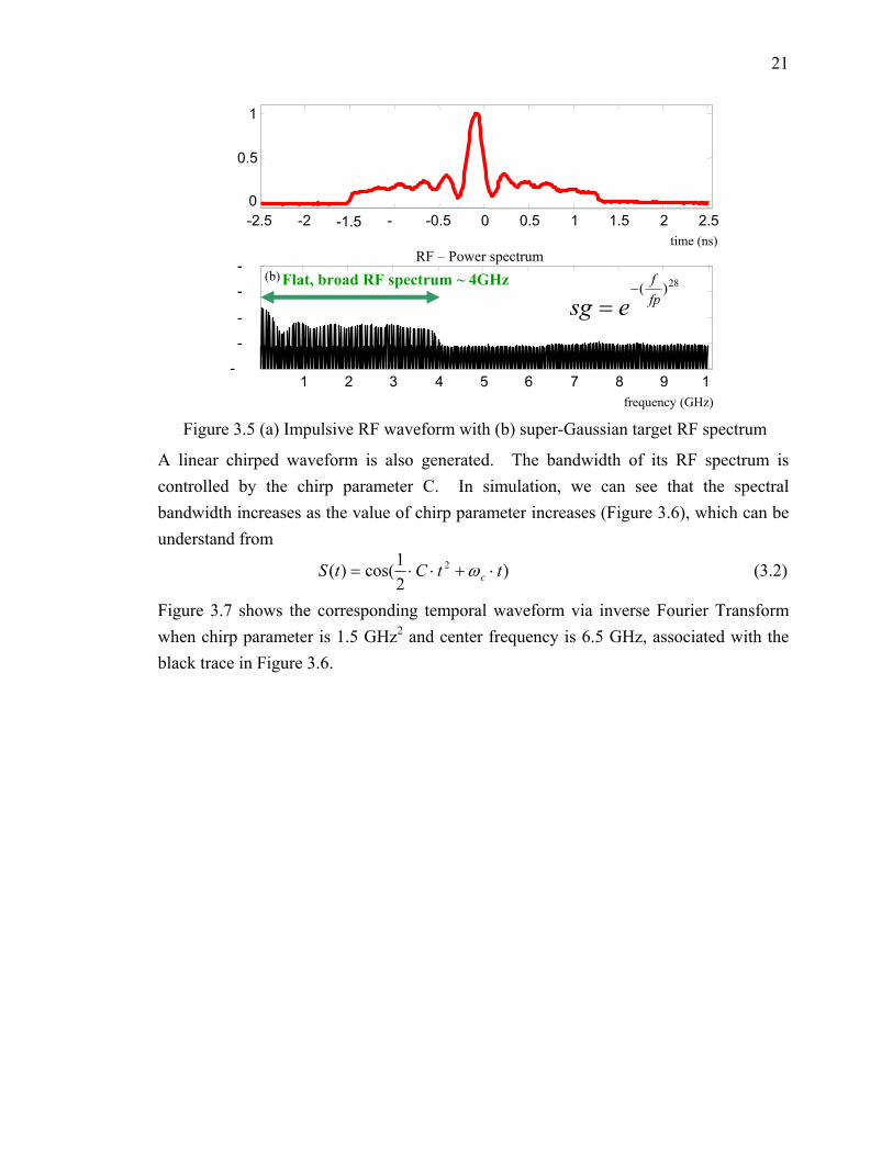
sampling the inverse Fourier transform of the target RF spectrum. Figure 3.5(a) shows the measured RF temporal waveform resulting from this operation. The impulsive waveform is approximately 450 ps (between first two nulls) and rides on a small dc pedestal (again, we are shaping the optical intensity). As shown in Figure 3.5(b), the RF power spectrum is very broad and shows a nearly super-Gaussian shape with a bandwidth of 3.2 GHz. The flatness is within 6.78 dB over spectral range from 0.59 GHz to 3.77 GHz, and the majority of this fluctuation results from the square-like DC pedestal in the time domain. This clearly illustrates our ability to tailor the RF spectrum of our waveforms to conform to the spectral requirements of a particular RF system. All waveforms presented so far exhibit peak amplitudes of 14 mV as determined by the input optical power (5 µW in average), photodiode responsivity, and 20 dB (power) electrical amplification.
RF – Time domain
(a)
21
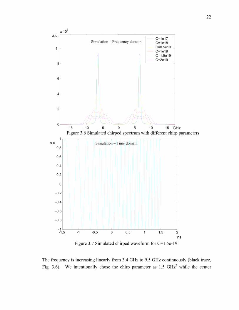
A linear chirped waveform is also generated. The bandwidth of its RF spectrum is controlled by the chirp parameter C. In simulation, we can see that the spectral bandwidth increases as the value of chirp parameter increases (Figure 3.6), which can be understand from
)21cos()( 2 ttCtS c ⋅+⋅⋅= ω
(3.2)
Figure 3.7 shows the corresponding temporal waveform via inverse Fourier Transform when chirp parameter is 1.5 GHz2 and center frequency is 6.5 GHz, associated with the black trace in Figure 3.6.
-2.5 -2 -1.5 - -0.5 0 0.5 1 1.5 2 2.50
0.5
1
1 2 3 4 5 6 7 8 9 1-
-
-
-
-
time (ns)
frequency (GHz)
Flat, broad RF spectrum ~ 4GHz 28)(fpf
esg−
=
RF – Power spectrum(b)
Figure 3.5 (a) Impulsive RF waveform with (b) super-Gaussian target RF spectrum
22
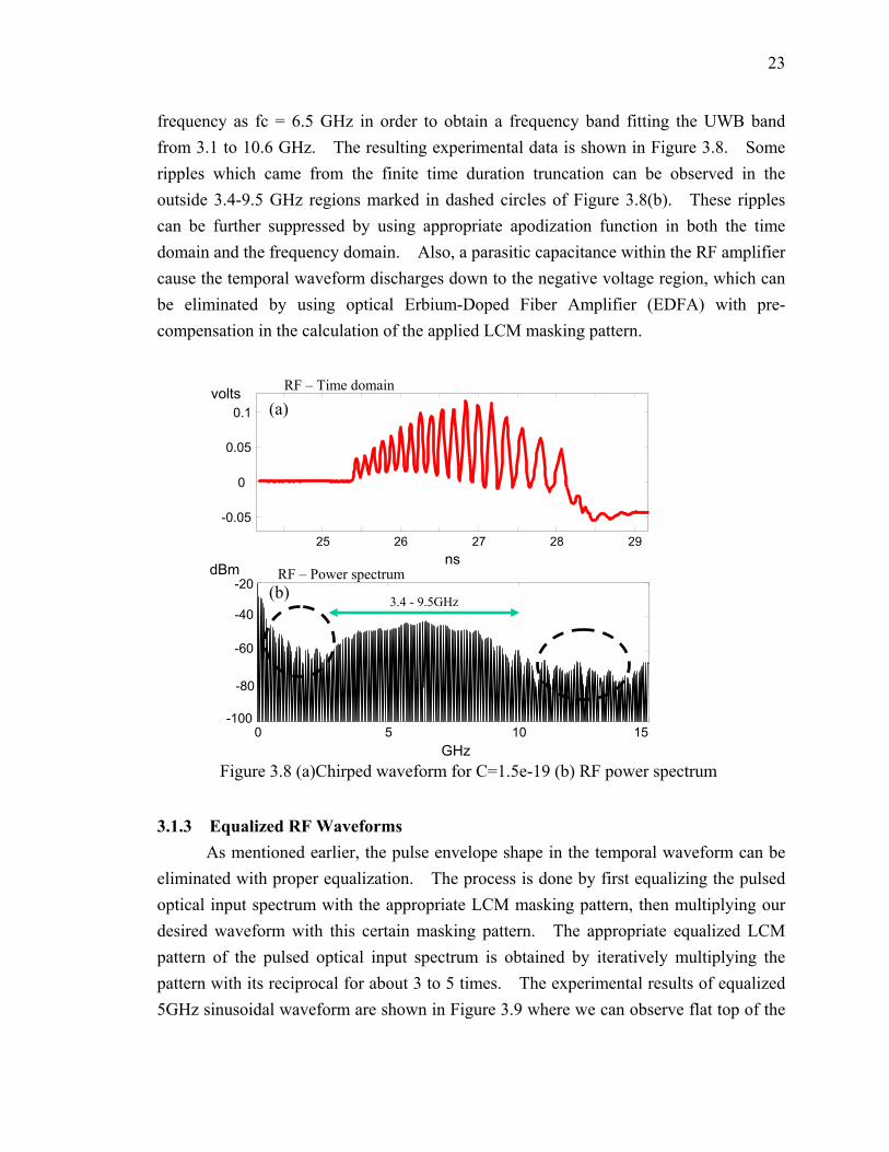
The frequency is increasing linearly from 3.4 GHz to 9.5 GHz continuously (black trace, Fig. 3.6). We intentionally chose the chirp parameter as 1.5 GHz2 while the center
-1.5 -1 -0.5 0 0.5 1 1.5 2 -1
-0.8
-0.6
-0.4
-0.2
0
0.2
0.4
0.6
0.8
1 Simulation – Time domain
-15 -10 -5 0 5 10 15 0
2
4
6
8
1
x 10 7 C=1e17 C=1e18 C=0.5e19 C=1e19 C=1.5e19 C=2e19
Simulation – Frequency domain a.u.
GHz
Figure 3.7 Simulated chirped waveform for C=1.5e-19
Figure 3.6 Simulated chirped spectrum with different chirp parameters
a.u.
ns
23
frequency as fc = 6.5 GHz in order to obtain a frequency band fitting the UWB band from 3.1 to 10.6 GHz. The resulting experimental data is shown in Figure 3.8. Some ripples which came from the finite time duration truncation can be observed in the outside 3.4-9.5 GHz regions marked in dashed circles of Figure 3.8(b). These ripples can be further suppressed by using appropriate apodization function in both the time domain and the frequency domain. Also, a parasitic capacitance within the RF amplifier cause the temporal waveform discharges down to the negative voltage region, which can be eliminated by using optical Erbium-Doped Fiber Amplifier (EDFA) with pre-compensation in the calculation of the applied LCM masking pattern.
3.1.3 Equalized RF Waveforms
As mentioned earlier, the pulse envelope shape in the temporal waveform can be eliminated with proper equalization. The process is done by first equalizing the pulsed optical input spectrum with the appropriate LCM masking pattern, then multiplying our desired waveform with this certain masking pattern. The appropriate equalized LCM pattern of the pulsed optical input spectrum is obtained by iteratively multiplying the pattern with its reciprocal for about 3 to 5 times. The experimental results of equalized 5GHz sinusoidal waveform are shown in Figure 3.9 where we can observe flat top of the
3.3-
25 26 27 28 29 -0.05
0
0.05
0.1
ns
0 5 10 15 -100
-80
-60
-40
-20
GHz
dBm
3.4 - 9.5GHz
(a)
(b) RF – Power spectrum
Figure 3.8 (a)Chirped waveform for C=1.5e-19 (b) RF power spectrum
volts RF – Time domain
24
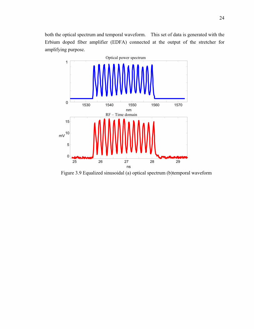
both the optical spectrum and temporal waveform. This set of data is generated with the Erbium doped fiber amplifier (EDFA) connected at the output of the stretcher for amplifying purpose.
25 26 27 28 29 0
5
10
15
ns
mV
1530 1540 1550 1560 1570 nm
RF – Time domain
0
Optical power spectrum 1
Figure 3.9 Equalized sinusoidal (a) optical spectrum (b)temporal waveform
25
3.2 Power Spectra Design and Generation
We exploit the RF spectral phase as a variable and demonstrate flat RF power
spectra in the UWB frequency band via arbitrarily shaped RF waveforms.
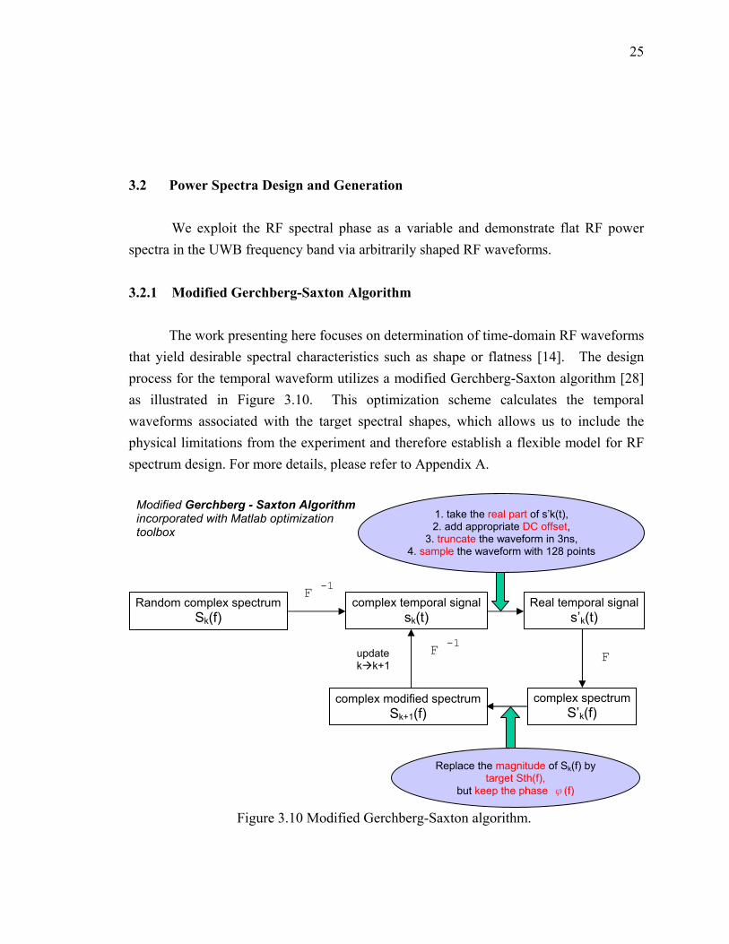
3.2.1 Modified Gerchberg-Saxton Algorithm The work presenting here focuses on determination of time-domain RF waveforms
that yield desirable spectral characteristics such as shape or flatness [14]. The design process for the temporal waveform utilizes a modified Gerchberg-Saxton algorithm [28] as illustrated in Figure 3.10. This optimization scheme calculates the temporal waveforms associated with the target spectral shapes, which allows us to include the physical limitations from the experiment and therefore establish a flexible model for RF spectrum design. For more details, please refer to Appendix A.
Modified Gerchberg - Saxton Algorithmincorporated with Matlab optimization toolbox
Replace the magnitude of Sk(f) by target Sth(f),
but keep the phase φ(f)
Random complex spectrum Sk(f)
complex spectrumS’k(f)
complex modified spectrumSk+1(f)
Real temporal signals’k(t)
1. take the real part of s’k(t), 2. add appropriate DC offset,
3. truncate the waveform in 3ns, 4. sample the waveform with 128 points
F -1 Fupdate k k+1
F -1complex temporal signal
sk(t)
Figure 3.10 Modified Gerchberg-Saxton algorithm.
26
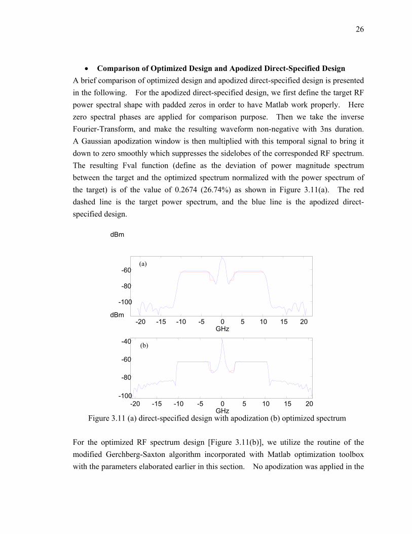
• Comparison of Optimized Design and Apodized Direct-Specified Design
A brief comparison of optimized design and apodized direct-specified design is presented in the following. For the apodized direct-specified design, we first define the target RF power spectral shape with padded zeros in order to have Matlab work properly. Here zero spectral phases are applied for comparison purpose. Then we take the inverse Fourier-Transform, and make the resulting waveform non-negative with 3ns duration. A Gaussian apodization window is then multiplied with this temporal signal to bring it down to zero smoothly which suppresses the sidelobes of the corresponded RF spectrum. The resulting Fval function (define as the deviation of power magnitude spectrum between the target and the optimized spectrum normalized with the power spectrum of the target) is of the value of 0.2674 (26.74%) as shown in Figure 3.11(a). The red dashed line is the target power spectrum, and the blue line is the apodized direct-specified design.
For the optimized RF spectrum design [Figure 3.11(b)], we utilize the routine of the modified Gerchberg-Saxton algorithm incorporated with Matlab optimization toolbox with the parameters elaborated earlier in this section. No apodization was applied in the
-20 -15 -10 -5 0 5 10 15 20
-100
-80
-60
GHz
dBm
-20 -15 -10 -5 0 5 10 15 20 -100
-80
-60
-40
GHz
dBm
(b)
(a)
Figure 3.11 (a) direct-specified design with apodization (b) optimized spectrum
27
optimization process. The resulting optimized RF spectrum came out after 6632 iterations with Fval equals 0.0528 (5.28%) as shown in Figure 3.11(b). In comparison, we have a level of improvement from 26.74% to 5.28% in error deviation. However, the computation time of this particular optimized design is around 1.54 minutes which is longer comparing to the direct specified method, 0.047 seconds. Please note that in both cases, the target spectrum is normalized in order to get more reliable estimates of Fval.
• Discussion of Optimization Approach In general, the optimization approach gives us a flexible model to calculate user-
defined spectrum provided existing constraints and seek for the optimized solution during the numerical process. The remaining challenge and problem of this optimization topic is to formulate an effective metric of energy efficiency control. The current results we have so far can only offer us the optimized spectrum but not the optimized energy performance yet. A couple of proposed solutions to the energy efficiency control will be introduced in Section 5.1.
3.2.2 Optimized Spectrum Generation
With this optimization method, we can generate RF spectrum with RF filter
features showing in the following. Figure 3.12 is an example of bandpass spectrum with a bandwidth of 3 GHz. In Figure 3.12(a), the purple dashed line is the target spectrum while the green curve is the optimized spectrum from simulation. The power spectrum in Figure 3.12(a) is the actual experimental data while Figure 3.12(b) is data of the associated temporal waveform.
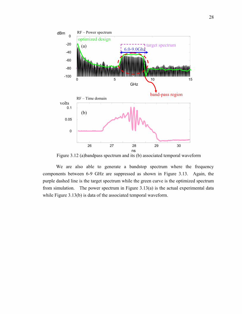
28
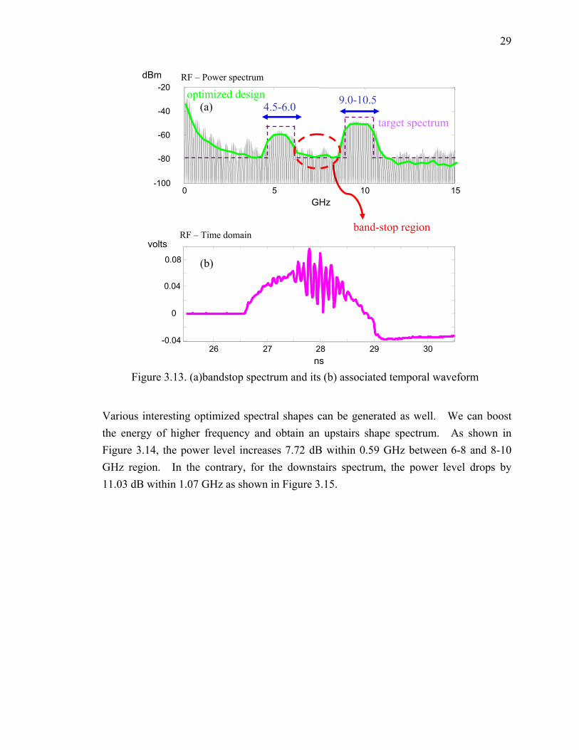
We are also able to generate a bandstop spectrum where the frequency
components between 6-9 GHz are suppressed as shown in Figure 3.13. Again, the purple dashed line is the target spectrum while the green curve is the optimized spectrum from simulation. The power spectrum in Figure 3.13(a) is the actual experimental data while Figure 3.13(b) is data of the associated temporal waveform.
26 27 28 29 30
0
0.05
0.1
ns
RF – Time domain band-pass region
dBm
15 0 5 10 -100
-80
-60
-40
-20
0
GHz
6.0-9.0Ghz
RF – Power spectrum
target spectrum optimized design
volts
(a)
(b)
Figure 3.12 (a)bandpass spectrum and its (b) associated temporal waveform
29
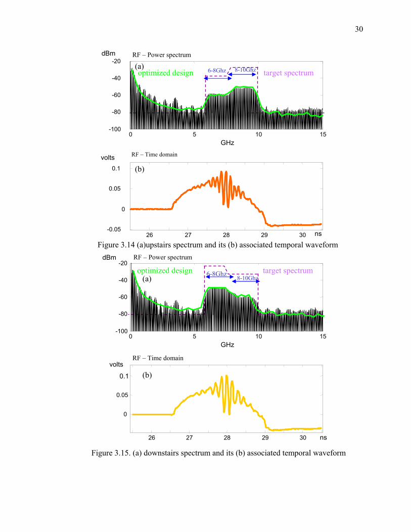
Various interesting optimized spectral shapes can be generated as well. We can boost the energy of higher frequency and obtain an upstairs shape spectrum. As shown in Figure 3.14, the power level increases 7.72 dB within 0.59 GHz between 6-8 and 8-10 GHz region. In the contrary, for the downstairs spectrum, the power level drops by 11.03 dB within 1.07 GHz as shown in Figure 3.15.
26 27 28 29 30 -0.04
0
0.04
0.08
ns
RF – Time domain band-stop region
0 5 10 15 -100
-80
-60
-40
-20
GHz
4.5-6.0 9.0-10.5
RF – Power spectrum
target spectrum
optimized design
volts
dBm
(a)
(b)
Figure 3.13. (a)bandstop spectrum and its (b) associated temporal waveform
30
0 5 10 15 -100
-80
-60
-40
-20
GHz
RF – Power spectrum
6-8Ghz 8-10Ghz
target spectrum optimized design
26 27 28 29 30
0
0.05
0.1
ns
volts RF – Time domain
dBm
(a)
(b)
0 5 10 15 -100
-80
-60
-40
-20
GHz
dBm RF – Power spectrum
6-8Ghz 8-10Ghz target spectrum optimized design
26 27 28 29 30 -0.05
0
0.05
0.1
ns
volts RF – Time domain
(a)
(b)
Figure 3.14 (a)upstairs spectrum and its (b) associated temporal waveform
Figure 3.15. (a) downstairs spectrum and its (b) associated temporal waveform
31
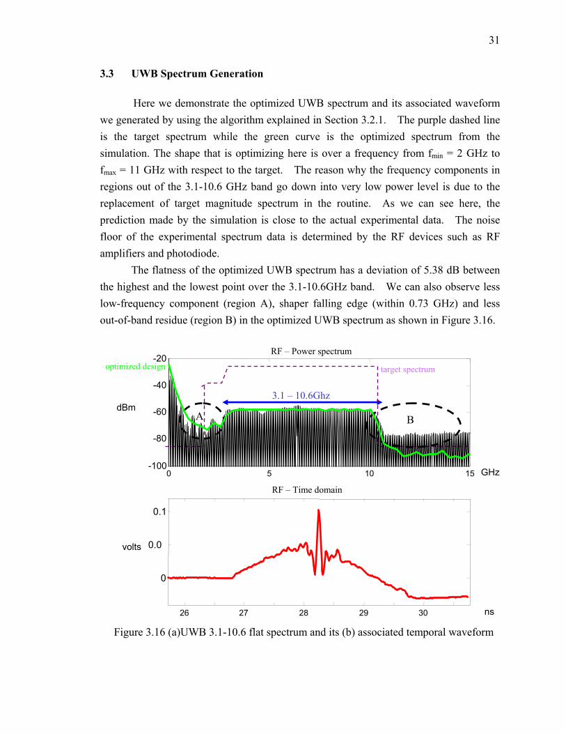
3.3 UWB Spectrum Generation
Here we demonstrate the optimized UWB spectrum and its associated waveform we generated by using the algorithm explained in Section 3.2.1. The purple dashed line is the target spectrum while the green curve is the optimized spectrum from the simulation. The shape that is optimizing here is over a frequency from fmin = 2 GHz to fmax = 11 GHz with respect to the target. The reason why the frequency components in regions out of the 3.1-10.6 GHz band go down into very low power level is due to the replacement of target magnitude spectrum in the routine. As we can see here, the prediction made by the simulation is close to the actual experimental data. The noise floor of the experimental spectrum data is determined by the RF devices such as RF amplifiers and photodiode.
The flatness of the optimized UWB spectrum has a deviation of 5.38 dB between the highest and the lowest point over the 3.1-10.6GHz band. We can also observe less low-frequency component (region A), shaper falling edge (within 0.73 GHz) and less out-of-band residue (region B) in the optimized UWB spectrum as shown in Figure 3.16.
0 5 10 15-100
-80
-60
-40
-20
GHz
dBm 3.1 – 10.6Ghz
RF – Power spectrum
target spectrum optimized design
26 27 28 29 30
0
0.0
0.1
ns
volts
RF – Time domain
A B
Figure 3.16 (a)UWB 3.1-10.6 flat spectrum and its (b) associated temporal waveform
32
4. CORRELATION DETECTION PROCESS THEORY In this chapter, we discuss theory of correlation detection process, some possible
experimental setups, and also its potential applications in UWB-CDMA transmission and detection.
4.1 Correlation Detection Experiential Configurations
It is very difficult to accomplish the ultrabroadband RF waveform processing using A/D (analog-to-digital) conversion and digital signal processing approaches for waveforms with instantaneous bandwidths reaching tens of GHz. As a result, it is highly desirable to realize analog methods allowing correlation processing of ultrabroadband RF waveforms.
In the previous work of our group, we have demonstrated optical correlation processing using a variety of techniques including FT pulse shapers [29-32], spectral holography [33], and nonlinear optics [34-35]. Here we proposed the RF photonics correlation processing using the Heterodyne receiver, which will be elaborated in the following.
4.1.1 Introduction to Mixers
Mixers use a nonlinear device to achieve frequency conversion of an input signal
[36]. A mixer uses the nonlinearity of a diode to generate an output spectrum consisting of the sum and difference frequencies of two input signals.
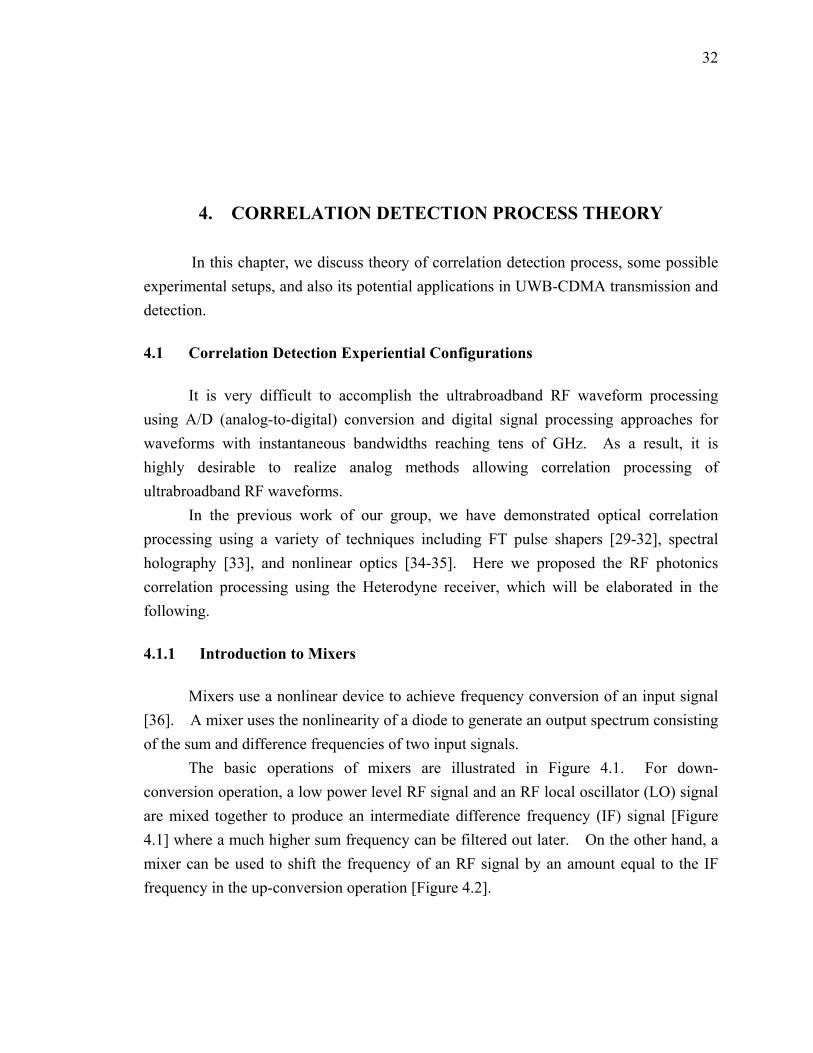
The basic operations of mixers are illustrated in Figure 4.1. For down-conversion operation, a low power level RF signal and an RF local oscillator (LO) signal are mixed together to produce an intermediate difference frequency (IF) signal [Figure 4.1] where a much higher sum frequency can be filtered out later. On the other hand, a mixer can be used to shift the frequency of an RF signal by an amount equal to the IF frequency in the up-conversion operation [Figure 4.2].
33
Some parameters of a practical mixer (Advanced Microwave Model #M3301) are given here. The bandwidth of the RF and LO port is around 18 GHz (from 4 to 22 GHz), and the bandwidth of IF port is around 3 GHz (from 0 to 3 GHz). 7 dBm average power is required for the LO level in order to ensure the mixer is in linear operating range. The typical conversion loss is 6 dB. The isolation between LO and RF is typically 30 dB and the isolation between LO and IF is typically 25 dB. Further explanation of these parameters can be found in the following.
• Conversion loss and Isolation
An important figure of merit for a mixer is the conversion loss, defined as
IF
RF
PP
Lc log10= (dB) (4.1)
where the PRF represents the available RF input power while the PIF represents the IF output power. In general, the conversion loss of practical mixers is between 4 and 7 dB. Minimum conversion loss usually occurs for LO powers between 0 and 10 dBm [37].
The leakage power level can be determined by using the Isolation parameter from the specification offered by the vendor. From LO port to IF port, the leakage level is PLO - Isolation(LO-IF) . Also, the leakage level from LO to RF port is PLO - Isolation(LO-RF) .
In addition to the conversion loss and isolation mentioned above, the impedance matching at the RF and LO inputs is important for signal sensitivity and noise figure.
I R
L
fLO
fIF fLO + fIF (= fRF) fLO - fIF
R I
L
fLO
fRF fRF - fLO (= fIF) fRF + fLO
Up-converter:
Figure 4.2 mixer operation: up-conversion
Down-converter:
Figure 4.1 mixer operation: down-conversion
34
Also, the suppression of higher-order harmonics is also an important characteristic that describes mixer performance.
• Image response For a given LO frequency, there will be two RF frequencies that mix down to the
same IF frequency. Assume the RF frequency is fRF = fLO+fIF, then the mixed output frequencies would be fRF + fLO and fRF - fLO , which are (2fLO+fIF) and (fIF) . Now, if we let the RF frequency be fRF = fIM = fLO-fIF, then the output frequencies of the mixer would be fRF + fLO and fRF - fLO , which are (2fLO-fIF) and (–fIF) . The latter output is the “image response” of the mixer which is indistinguishable from the direct response. This can be eliminated by filtering out the fIM component at the input of the mixer. For a broadband signal, this effect has to be carefully handled by confining all the fRF components to the frequency ranges greater than fLO, or by confining all the fRF components to the frequency ranges less than fLO.
• Intermodulation products
The nonlinearity of the mixer not only makes the frequency conversion possible, but also gives rise to a number of undesired harmonics and mixer products, which increase the conversion loss of a mixer and lead to a signal distortion. In general, a system using a nonlinear device has a voltage transfer function written as
...3
32
210 ++++= inininout VaVaVaaV (4.2)
For a mixer, the a0 term corresponds to the DC bias voltage, while the desired mixed output is part of the Vin
2 term. If the input to the system consists of a single frequency (or tone), Vin=cos(ω1t), then the output voltage will consist of all harmonics, mω1, of the input signal. In a mixer application, these single-tone distortion products are generally eliminated by filtering.
More serious problems arise when the input to the system consists of two relatively closely spaced frequencies (two-tone), Vin=cos(ω1t)+cos(ω2t). Then the output spectrum will consist of all harmonics, mω1+nω2, where m and n may be positive or negative integers. The Vin
2 will produce harmonics at the frequencies 2ω1, 2ω2, ω1-ω2, ω1+ω2. Usually ω1-ω2 is the desired result for a mixer while the rest frequency components can be filtered. The Vin
3 will produce harmonics at the frequencies 3ω1, 3ω2, 2ω1+ω2, ω1+2ω2, which can be filtered, and 2ω1-ω2, 2ω2-ω1, which generally cannot be
35
filtered as they may not be far away from the desired result ω1-ω2. Such products are called intermodulation distortion. The third-order two-tone intermodulation products 2ω1-ω2, 2ω2-ω1 are especially important because they may set the dynamic range or bandwidth of the system.
4.1.2 AWG Transmitter and Heterodyne Receiver
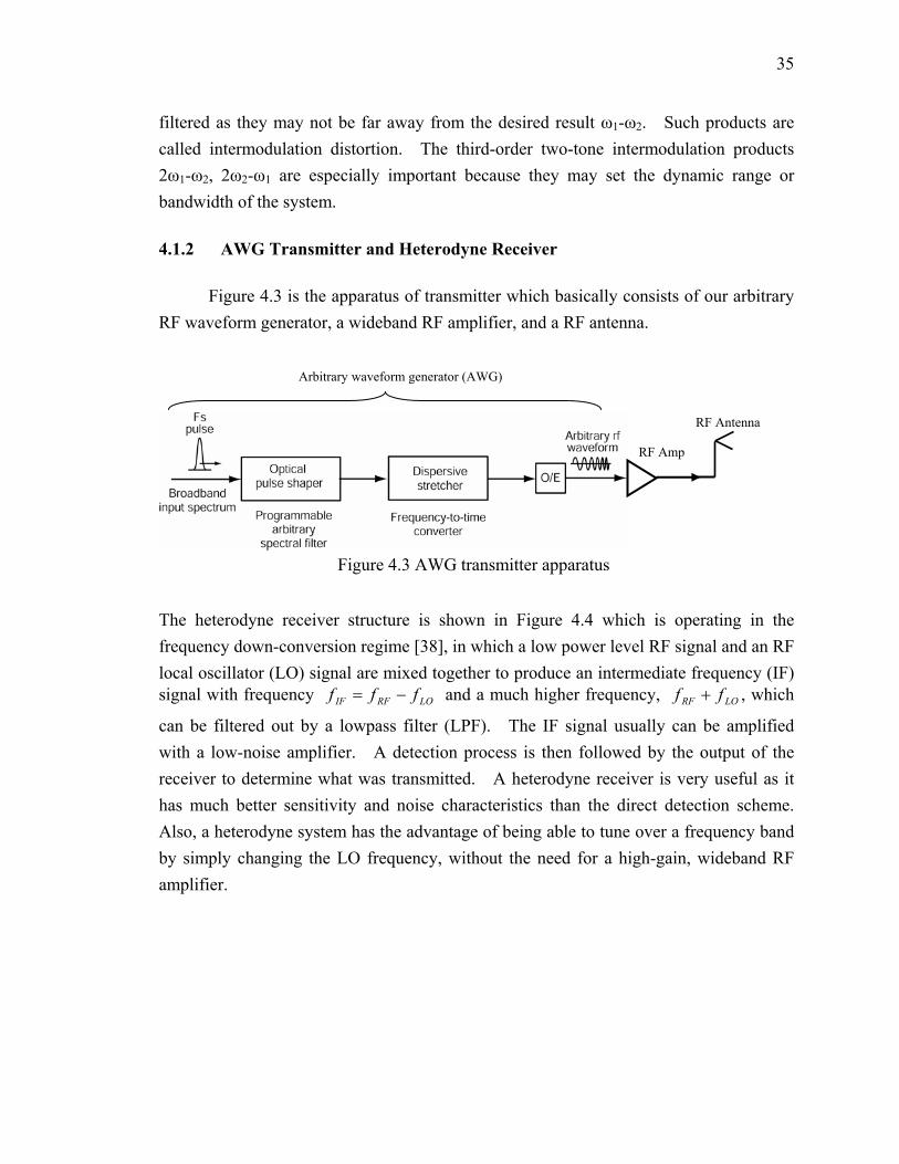
Figure 4.3 is the apparatus of transmitter which basically consists of our arbitrary
RF waveform generator, a wideband RF amplifier, and a RF antenna.
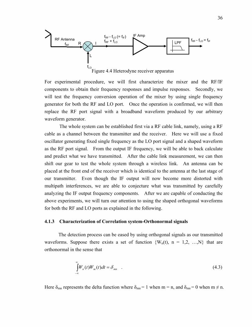
The heterodyne receiver structure is shown in Figure 4.4 which is operating in the frequency down-conversion regime [38], in which a low power level RF signal and an RF local oscillator (LO) signal are mixed together to produce an intermediate frequency (IF) signal with frequency LORFIF fff −= and a much higher frequency, LORF ff + , which
can be filtered out by a lowpass filter (LPF). The IF signal usually can be amplified with a low-noise amplifier. A detection process is then followed by the output of the receiver to determine what was transmitted. A heterodyne receiver is very useful as it has much better sensitivity and noise characteristics than the direct detection scheme. Also, a heterodyne system has the advantage of being able to tune over a frequency band by simply changing the LO frequency, without the need for a high-gain, wideband RF amplifier.
RF Amp
RF Antenna
Arbitrary waveform generator (AWG)
Figure 4.3 AWG transmitter apparatus
36
For experimental procedure, we will first characterize the mixer and the RF/IF components to obtain their frequency responses and impulse responses. Secondly, we will test the frequency conversion operation of the mixer by using single frequency generator for both the RF and LO port. Once the operation is confirmed, we will then replace the RF port signal with a broadband waveform produced by our arbitrary waveform generator.
The whole system can be established first via a RF cable link, namely, using a RF cable as a channel between the transmitter and the receiver. Here we will use a fixed oscillator generating fixed single frequency as the LO port signal and a shaped waveform as the RF port signal. From the output IF frequency, we will be able to back calculate and predict what we have transmitted. After the cable link measurement, we can then shift our gear to test the whole system through a wireless link. An antenna can be placed at the front end of the receiver which is identical to the antenna at the last stage of our transmitter. Even though the IF output will now become more distorted with multipath interferences, we are able to conjecture what was transmitted by carefully analyzing the IF output frequency components. After we are capable of conducting the above experiments, we will turn our attention to using the shaped orthogonal waveforms for both the RF and LO ports as explained in the following. 4.1.3 Characterization of Correlation system-Orthonormal signals
The detection process can be eased by using orthogonal signals as our transmitted
waveforms. Suppose there exists a set of function {Wn(t), n = 1,2, …,N} that are orthonormal in the sense that
∫∞
∞−
= mnmn dttWtW δ)()( . (4.3)
Here δmn represents the delta function where δmn = 1 when m = n, and δmn = 0 when m ≠ n.
R I
L
fRF
fRF - fLO (= fIF) fRF + fLO
LPF
fRF - fLO = fIF
IF Amp RF Antenna
fLO Figure 4.4 Heterodyne receiver apparatus
37
• Orthonormal Expansions of Signal The Gram-Schmidt procedure [39] allows us to calculate, and therefore, construct a
set of orthonormal waveforms. Assume we have a set of signal waveforms {si(t), i = 1,2, …,M} which are deterministic, real-valued signal with finite energy. The energy of the first waveform s1(t) is
∫∞
∞−
= dtts 211 )]([ε . (4.4)
The first orthonormal waveform W1(t) is simply constructed as s1(t) normalized to unit energy, which is
1
11
)()(εtstW = . (4.5)
The second waveform is constructed from s2(t) by first computing the projection of W1(t) onto s2(t)
∫∞
∞−
= dttWtsc )()( 1212 . (4.6)
Then a waveform W’
2(t) that is orthogonal to W1(t) can be obtained
)()()(' 11222 tWctstW −= . (4.7)
Let ε2 denotes the energy of W’
2(t), the normalized waveform that is orthogonal to W1(t) becomes
2
22
)(')(
εtW
tW =
(4.8)
In general, the orthogonalization of the kth function leads to
k
kk
tWtW
ε)('
)( =
(4.9)
38
where
∑−
=
−=1
1)()()('
k
iiikkk tWctstW
(4.10)
and
∫∞
∞−
= dttWtsc ikik )()( , i = 1,2,…,k-1 (4.11)
This orthogonalization process is continued until all the M signal waveforms {si(t)} have been exhausted and N (≤M) orthonormal waveforms {Wn(t)} have been constructed. The dimensionality N of the signal space will be equal to M if all the signal waveforms are linearly independent.
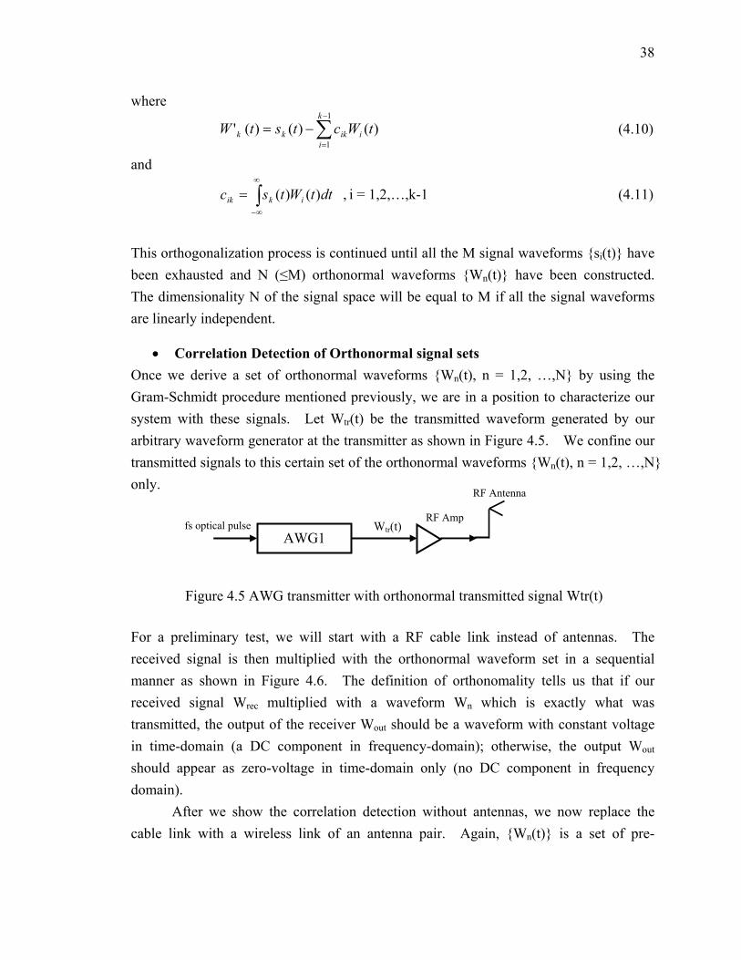
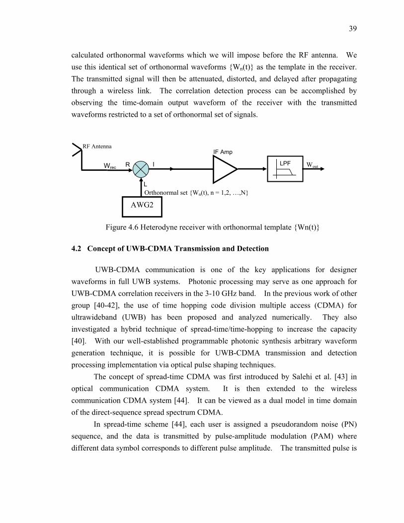
• Correlation Detection of Orthonormal signal sets Once we derive a set of orthonormal waveforms {Wn(t), n = 1,2, …,N} by using the Gram-Schmidt procedure mentioned previously, we are in a position to characterize our system with these signals. Let Wtr(t) be the transmitted waveform generated by our arbitrary waveform generator at the transmitter as shown in Figure 4.5. We confine our transmitted signals to this certain set of the orthonormal waveforms {Wn(t), n = 1,2, …,N} only. For a preliminary test, we will start with a RF cable link instead of antennas. The received signal is then multiplied with the orthonormal waveform set in a sequential manner as shown in Figure 4.6. The definition of orthonomality tells us that if our received signal Wrec multiplied with a waveform Wn which is exactly what was transmitted, the output of the receiver Wout should be a waveform with constant voltage in time-domain (a DC component in frequency-domain); otherwise, the output Wout
should appear as zero-voltage in time-domain only (no DC component in frequency domain).
After we show the correlation detection without antennas, we now replace the cable link with a wireless link of an antenna pair. Again, {Wn(t)} is a set of pre-
RF Amp
RF Antenna
AWG1 fs optical pulse Wtr(t)
Figure 4.5 AWG transmitter with orthonormal transmitted signal Wtr(t)
39
calculated orthonormal waveforms which we will impose before the RF antenna. We use this identical set of orthonormal waveforms {Wn(t)} as the template in the receiver. The transmitted signal will then be attenuated, distorted, and delayed after propagating through a wireless link. The correlation detection process can be accomplished by observing the time-domain output waveform of the receiver with the transmitted waveforms restricted to a set of orthonormal set of signals.
4.2 Concept of UWB-CDMA Transmission and Detection
UWB-CDMA communication is one of the key applications for designer
waveforms in full UWB systems. Photonic processing may serve as one approach for UWB-CDMA correlation receivers in the 3-10 GHz band. In the previous work of other group [40-42], the use of time hopping code division multiple access (CDMA) for ultrawideband (UWB) has been proposed and analyzed numerically. They also investigated a hybrid technique of spread-time/time-hopping to increase the capacity [40]. With our well-established programmable photonic synthesis arbitrary waveform generation technique, it is possible for UWB-CDMA transmission and detection processing implementation via optical pulse shaping techniques.
The concept of spread-time CDMA was first introduced by Salehi et al. [43] in optical communication CDMA system. It is then extended to the wireless communication CDMA system [44]. It can be viewed as a dual model in time domain of the direct-sequence spread spectrum CDMA.
In spread-time scheme [44], each user is assigned a pseudorandom noise (PN) sequence, and the data is transmitted by pulse-amplitude modulation (PAM) where different data symbol corresponds to different pulse amplitude. The transmitted pulse is
R I
L
Wrec
LPF Wout
IF Amp
Orthonormal set {Wn(t), n = 1,2, …,N}
RF Antenna
AWG2
Figure 4.6 Heterodyne receiver with orthonormal template {Wn(t)}
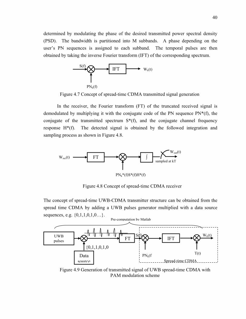
40
determined by modulating the phase of the desired transmitted power spectral density (PSD). The bandwidth is partitioned into M subbands. A phase depending on the user’s PN sequences is assigned to each subband. The temporal pulses are then obtained by taking the inverse Fourier transform (IFT) of the corresponding spectrum.
In the receiver, the Fourier transform (FT) of the truncated received signal is
demodulated by multiplying it with the conjugate code of the PN sequence PN*(f), the conjugate of the transmitted spectrum S*(f), and the conjugate channel frequency response H*(f). The detected signal is obtained by the followed integration and sampling process as shown in Figure 4.8.
The concept of spread-time UWB-CDMA transmitter structure can be obtained from the spread time CDMA by adding a UWB pulses generator multiplied with a data source sequences, e.g. {0,1,1,0,1,0…}.
IFT S(f)
Wk(t)
PNk(f)
Figure 4.7 Concept of spread-time CDMA transmitted signal generation
FT Wrec(t) Wout(t)
PNk*(f)S*(f)H*(f)
∫ sampled at kT
Figure 4.8 Concept of spread-time CDMA receiver
FT
PNk(f
UWB pulses IFT
Data source
T(t)
Wk(t)S(f)
Spread-time CDMA
Figure 4.9 Generation of transmitted signal of UWB spread-time CDMA with PAM modulation scheme
Pre-computation by Matlab
{0,1,1,0,1,0
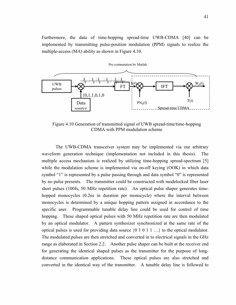
41
Furthermore, the data of time-hopping spread-time UWB-CDMA [40] can be implemented by transmitting pulse-position modulation (PPM) signals to realize the multiple-access (MA) ability as shown in Figure 4.10.
The UWB-CDMA transceiver system may be implemented via our arbitrary
waveform generation technique (implementation not included in this thesis). The multiple access mechanism is realized by utilizing time-hopping spread-spectrum [5] while the modulation scheme is implemented via on-off keying (OOK) in which data symbol “1” is represented by a pulse passing through and data symbol “0” is represented by no pulse presents. The transmitter could be constructed with modelocked fiber laser short pulses (100fs, 50 MHz repetition rate). An optical pulse shaper generates time-hopped monocycles (0.2ns in duration per monocycle) where the interval between monocycles is determined by a unique hopping pattern assigned in accordance to the specific user. Programmable tunable delay line could be used for control of time hopping. These shaped optical pulses with 50 MHz repetition rate are then modulated by an optical modulator. A pattern synthesizer synchronized at the same rate of the optical pulses is used for providing data source {0 1 0 1 1 …} to the optical modulator. The modulated pulses are then stretched and converted in to electrical signals in the GHz range as elaborated in Section 2.2. Another pulse shaper can be built at the receiver end for generating the identical shaped pulses as the transmitter for the purpose of long-distance communication applications. These optical pulses are also stretched and converted in the identical way of the transmitter. A tunable delay line is followed to
Figure 4.10 Generation of transmitted signal of UWB spread-time/time-hopping CDMA with PPM modulation scheme
FT
PNk(f)
UWB pulses IFT
Data source
T(t)
Wk(t)S(f)
Spread-time CDMA
Pre-computation by Matlab
{0,1,1,0,1,0
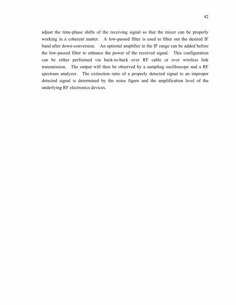
42
adjust the time-phase shifts of the receiving signal so that the mixer can be properly working in a coherent matter. A low-passed filter is used to filter out the desired IF band after down-conversion. An optional amplifier in the IF range can be added before the low-passed filter to enhance the power of the received signal. This configuration can be either performed via back-to-back over RF cable or over wireless link transmission. The output will then be observed by a sampling oscilloscope and a RF spectrum analyzer. The extinction ratio of a properly detected signal to an improper detected signal is determined by the noise figure and the amplification level of the underlying RF electronics devices.
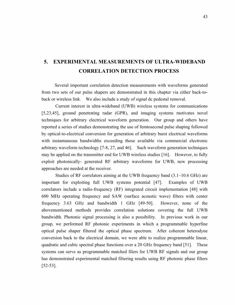
43
5. EXPERIMENTAL MEASUREMENTS OF ULTRA-WIDEBAND
CORRELATION DETECTION PROCESS Several important correlation detection measurements with waveforms generated
from two sets of our pulse shapers are demonstrated in this chapter via either back-to-back or wireless link. We also include a study of signal dc pedestal removal. Current interest in ultra-wideband (UWB) wireless systems for communications [5,23,45], ground penetrating radar (GPR), and imaging systems motivates novel techniques for arbitrary electrical waveform generation. Our group and others have reported a series of studies demonstrating the use of femtosecond pulse shaping followed by optical-to-electrical conversion for generation of arbitrary burst electrical waveforms with instantaneous bandwidths exceeding those available via commercial electronic arbitrary waveform technology [7-8, 27, and 46]. Such waveform generation techniques may be applied on the transmitter end for UWB wireless studies [16]. However, to fully exploit photonically- generated RF arbitrary waveforms for UWB, new processing approaches are needed at the receiver. Studies of RF correlators aiming at the UWB frequency band (3.1–10.6 GHz) are important for exploiting full UWB systems potential [47]. Examples of UWB correlators include a radio-frequency (RF) integrated circuit implementation [48] with 600 MHz operating frequency and SAW (surface acoustic wave) filters with center frequency 3.63 GHz and bandwidth 1 GHz [49-50]. However, none of the abovementioned methods provides correlation solutions covering the full UWB bandwidth. Photonic signal processing is also a possibility. In previous work in our group, we performed RF photonic experiments in which a programmable hyperfine optical pulse shaper filtered the optical phase spectrum. After coherent heterodyne conversion back to the electrical domain, we were able to realize programmable linear, quadratic and cubic spectral phase functions over a 20 GHz frequency band [51]. These systems can serve as programmable matched filers for UWB RF signals and our group has demonstrated experimental matched filtering results using RF photonic phase filters [52-53].
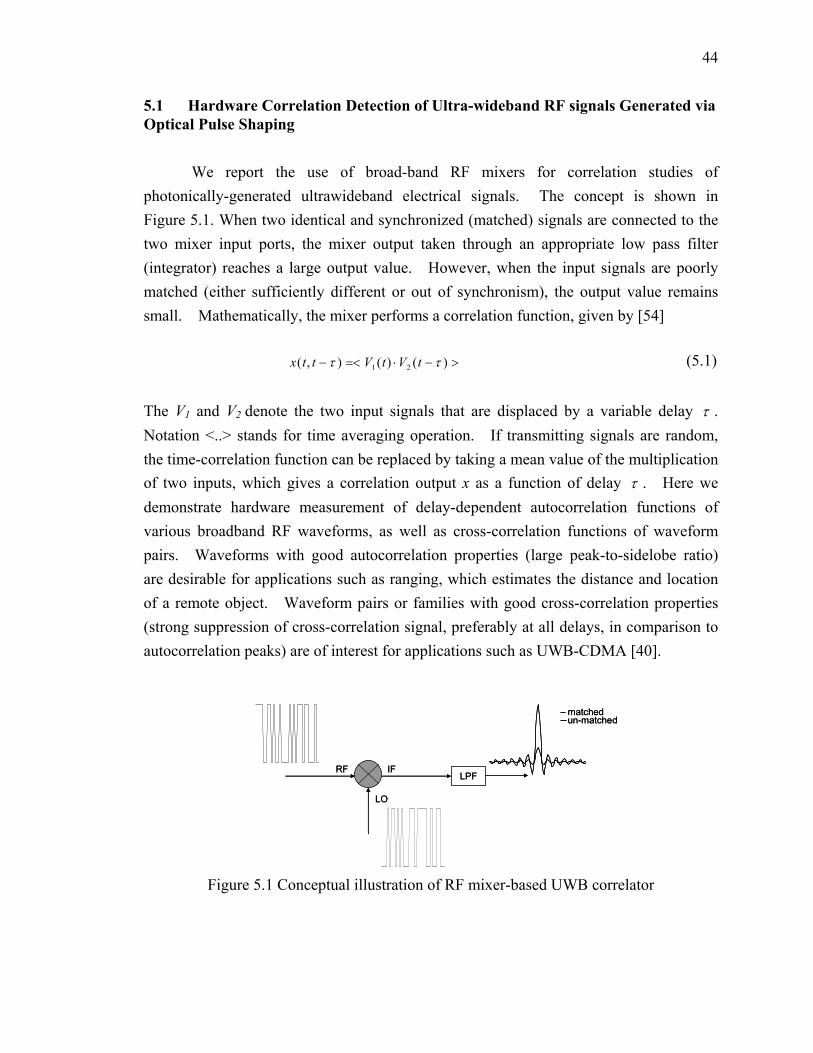
44
5.1 Hardware Correlation Detection of Ultra-wideband RF signals Generated via Optical Pulse Shaping We report the use of broad-band RF mixers for correlation studies of photonically-generated ultrawideband electrical signals. The concept is shown in Figure 5.1. When two identical and synchronized (matched) signals are connected to the two mixer input ports, the mixer output taken through an appropriate low pass filter (integrator) reaches a large output value. However, when the input signals are poorly matched (either sufficiently different or out of synchronism), the output value remains small. Mathematically, the mixer performs a correlation function, given by [54]
>−⋅=<− )()(),( 21 ττ tVtVttx (5.1)
The V1 and V2 denote the two input signals that are displaced by a variable delay τ . Notation <..> stands for time averaging operation. If transmitting signals are random, the time-correlation function can be replaced by taking a mean value of the multiplication of two inputs, which gives a correlation output x as a function of delay τ . Here we demonstrate hardware measurement of delay-dependent autocorrelation functions of various broadband RF waveforms, as well as cross-correlation functions of waveform pairs. Waveforms with good autocorrelation properties (large peak-to-sidelobe ratio) are desirable for applications such as ranging, which estimates the distance and location of a remote object. Waveform pairs or families with good cross-correlation properties (strong suppression of cross-correlation signal, preferably at all delays, in comparison to autocorrelation peaks) are of interest for applications such as UWB-CDMA [40].
RF IF
LO
LPF
matchedun-matched
RF IF
LO
LPF
matchedun-matched
Figure 5.1 Conceptual illustration of RF mixer-based UWB correlator
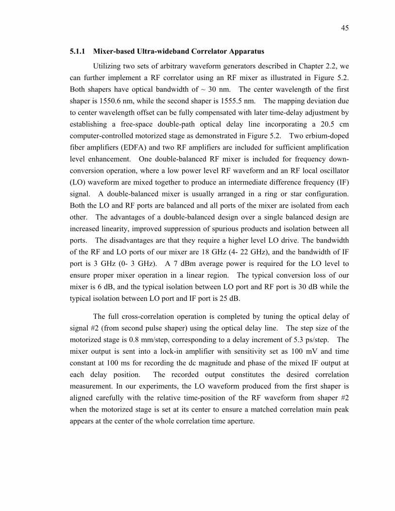
45
5.1.1 Mixer-based Ultra-wideband Correlator Apparatus
Utilizing two sets of arbitrary waveform generators described in Chapter 2.2, we can further implement a RF correlator using an RF mixer as illustrated in Figure 5.2. Both shapers have optical bandwidth of ~ 30 nm. The center wavelength of the first shaper is 1550.6 nm, while the second shaper is 1555.5 nm. The mapping deviation due to center wavelength offset can be fully compensated with later time-delay adjustment by establishing a free-space double-path optical delay line incorporating a 20.5 cm computer-controlled motorized stage as demonstrated in Figure 5.2. Two erbium-doped fiber amplifiers (EDFA) and two RF amplifiers are included for sufficient amplification level enhancement. One double-balanced RF mixer is included for frequency down-conversion operation, where a low power level RF waveform and an RF local oscillator (LO) waveform are mixed together to produce an intermediate difference frequency (IF) signal. A double-balanced mixer is usually arranged in a ring or star configuration. Both the LO and RF ports are balanced and all ports of the mixer are isolated from each other. The advantages of a double-balanced design over a single balanced design are increased linearity, improved suppression of spurious products and isolation between all ports. The disadvantages are that they require a higher level LO drive. The bandwidth of the RF and LO ports of our mixer are 18 GHz (4- 22 GHz), and the bandwidth of IF port is 3 GHz (0- 3 GHz). A 7 dBm average power is required for the LO level to ensure proper mixer operation in a linear region. The typical conversion loss of our mixer is 6 dB, and the typical isolation between LO port and RF port is 30 dB while the typical isolation between LO port and IF port is 25 dB.
The full cross-correlation operation is completed by tuning the optical delay of signal #2 (from second pulse shaper) using the optical delay line. The step size of the motorized stage is 0.8 mm/step, corresponding to a delay increment of 5.3 ps/step. The mixer output is sent into a lock-in amplifier with sensitivity set as 100 mV and time constant at 100 ms for recording the dc magnitude and phase of the mixed IF output at each delay position. The recorded output constitutes the desired correlation measurement. In our experiments, the LO waveform produced from the first shaper is aligned carefully with the relative time-position of the RF waveform from shaper #2 when the motorized stage is set at its center to ensure a matched correlation main peak appears at the center of the whole correlation time aperture.
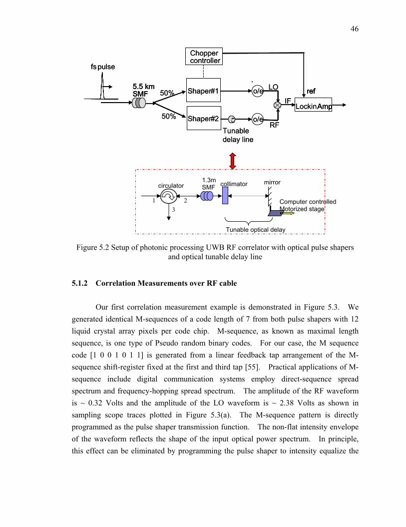
46
Figure 5.2 Setup of photonic processing UWB RF correlator with optical pulse shapers
and optical tunable delay line
5.1.2 Correlation Measurements over RF cable Our first correlation measurement example is demonstrated in Figure 5.3. We generated identical M-sequences of a code length of 7 from both pulse shapers with 12 liquid crystal array pixels per code chip. M-sequence, as known as maximal length sequence, is one type of Pseudo random binary codes. For our case, the M sequence code [1 0 0 1 0 1 1] is generated from a linear feedback tap arrangement of the M-sequence shift-register fixed at the first and third tap [55]. Practical applications of M-sequence include digital communication systems employ direct-sequence spread spectrum and frequency-hopping spread spectrum. The amplitude of the RF waveform is ~ 0.32 Volts and the amplitude of the LO waveform is ~ 2.38 Volts as shown in sampling scope traces plotted in Figure 5.3(a). The M-sequence pattern is directly programmed as the pulse shaper transmission function. The non-flat intensity envelope of the waveform reflects the shape of the input optical power spectrum. In principle, this effect can be eliminated by programming the pulse shaper to intensity equalize the
1.3mSMF collimator
1 3
circulator
2
mirror
Computer controlledMotorized stage
Tunable optical delay
5.5 km SMF
Lockin Amp
LO
IF 50%
50%
fs pulse
Chopper controller
ref .
RF
Shaper#15.5 km SMF
Amp
ح
Tunable delay line
ref .
Shaper#2
o/e
o/e
5.5 km SMF
Lockin Amp
LO
IF 50%
50%
fs pulse
Chopper controller
ref .
RF
Shaper#15.5 km SMF
Amp
ح
Tunable delay line
ref .
Shaper#2
o/e
o/e
47
optical spectrum; however, such equalization is not included in the current experiments as it induces ripples in RF spectrum and also lower the signal energy. The decay at the trailing edge of the temporal waveforms is attributed to the response of the RF amplifiers that we used.
-0.6 -0.4 -0.2 0 0.2 0.4 0.6
-40
-20
0
20
40
60
Time(ns)
mV
-2.5 -2 -1.5 -1 -0.5 0 0.5 1 1.5 2 2.5
0
1
2
3
Time(ns)
Vol
ts
M7 -LOM7 -RF
a
b
-0.6 -0.4 -0.2 0 0.2 0.4 0.6
-40
-20
0
20
40
60
Time(ns)
mV
-2.5 -2 -1.5 -1 -0.5 0 0.5 1 1.5 2 2.5
0
1
2
3
Time(ns)
Vol
ts
M7 -LOM7 -RF
a
b
Figure 5.3 M-sequence of 7 bits (a) generated RF waveforms, solid: shaper #1 dashed:
shaper #2; (b) correlation measurement Figure 5.3(b) shows the autocorrelation measurement [56] obtained with these nominally identical M-sequences of code length 7. A nice peak can be observed at the zero relative delay position, while only small side-lobes are observed at other delay positions. Note that although the input waveforms are both positive definite, the correlation signal is bipolar and centered at zero voltage. This occurs because of the band pass filtering effect of the mixer on the input RF and LO signals. To evaluate the performance of the correlation function, we define an extinction ratio (ER) for matched (autocorrelation) case as the ratio of the signal main peak to its maximum side-lobe. Assuming perfect correlation operation, this is really a property of the tested waveform. For these M-sequences of length 7, we obtain an extinction ratio as ~ 5.81 dB. The width of the correlation peak is 96 ps. The inverse of the peak width is of order 10 GHz, which shows that the bandwidth of our waveform generation and processing system is comparable to the bandwidth of the full UWB band. To explore the versatility of our setup, we also designed uniform distributed random sequences. A pair of random sequence of length 7 is selected by the following method via software calculation. First, we self-correlated the sequence generated
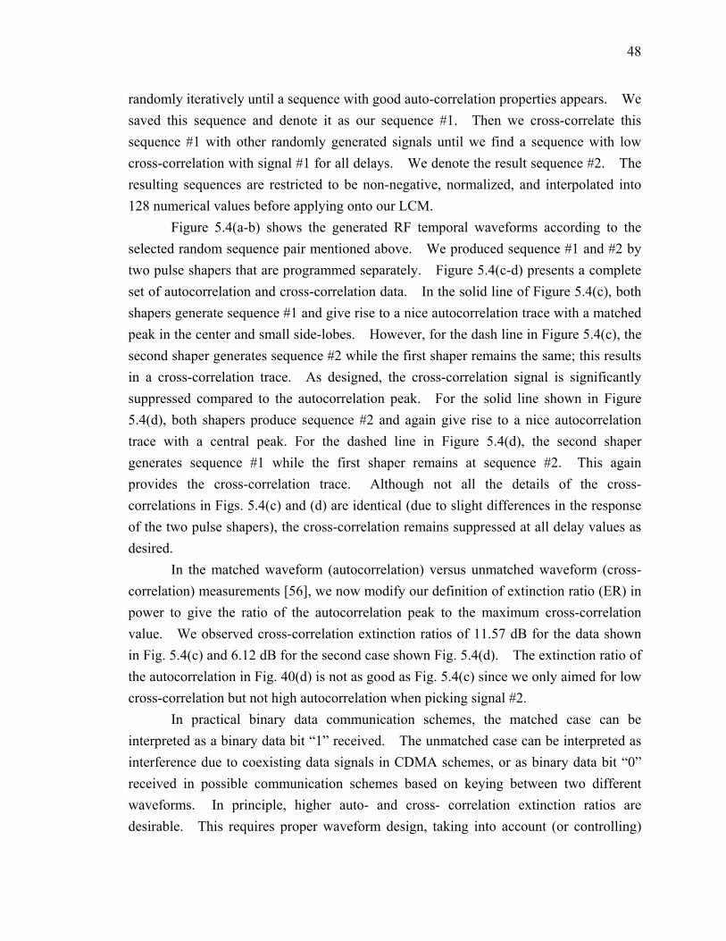
48
randomly iteratively until a sequence with good auto-correlation properties appears. We saved this sequence and denote it as our sequence #1. Then we cross-correlate this sequence #1 with other randomly generated signals until we find a sequence with low cross-correlation with signal #1 for all delays. We denote the result sequence #2. The resulting sequences are restricted to be non-negative, normalized, and interpolated into 128 numerical values before applying onto our LCM. Figure 5.4(a-b) shows the generated RF temporal waveforms according to the selected random sequence pair mentioned above. We produced sequence #1 and #2 by two pulse shapers that are programmed separately. Figure 5.4(c-d) presents a complete set of autocorrelation and cross-correlation data. In the solid line of Figure 5.4(c), both shapers generate sequence #1 and give rise to a nice autocorrelation trace with a matched peak in the center and small side-lobes. However, for the dash line in Figure 5.4(c), the second shaper generates sequence #2 while the first shaper remains the same; this results in a cross-correlation trace. As designed, the cross-correlation signal is significantly suppressed compared to the autocorrelation peak. For the solid line shown in Figure 5.4(d), both shapers produce sequence #2 and again give rise to a nice autocorrelation trace with a central peak. For the dashed line in Figure 5.4(d), the second shaper generates sequence #1 while the first shaper remains at sequence #2. This again provides the cross-correlation trace. Although not all the details of the cross-correlations in Figs. 5.4(c) and (d) are identical (due to slight differences in the response of the two pulse shapers), the cross-correlation remains suppressed at all delay values as desired. In the matched waveform (autocorrelation) versus unmatched waveform (cross-correlation) measurements [56], we now modify our definition of extinction ratio (ER) in power to give the ratio of the autocorrelation peak to the maximum cross-correlation value. We observed cross-correlation extinction ratios of 11.57 dB for the data shown in Fig. 5.4(c) and 6.12 dB for the second case shown Fig. 5.4(d). The extinction ratio of the autocorrelation in Fig. 40(d) is not as good as Fig. 5.4(c) since we only aimed for low cross-correlation but not high autocorrelation when picking signal #2. In practical binary data communication schemes, the matched case can be interpreted as a binary data bit “1” received. The unmatched case can be interpreted as interference due to coexisting data signals in CDMA schemes, or as binary data bit “0” received in possible communication schemes based on keying between two different waveforms. In principle, higher auto- and cross- correlation extinction ratios are desirable. This requires proper waveform design, taking into account (or controlling)
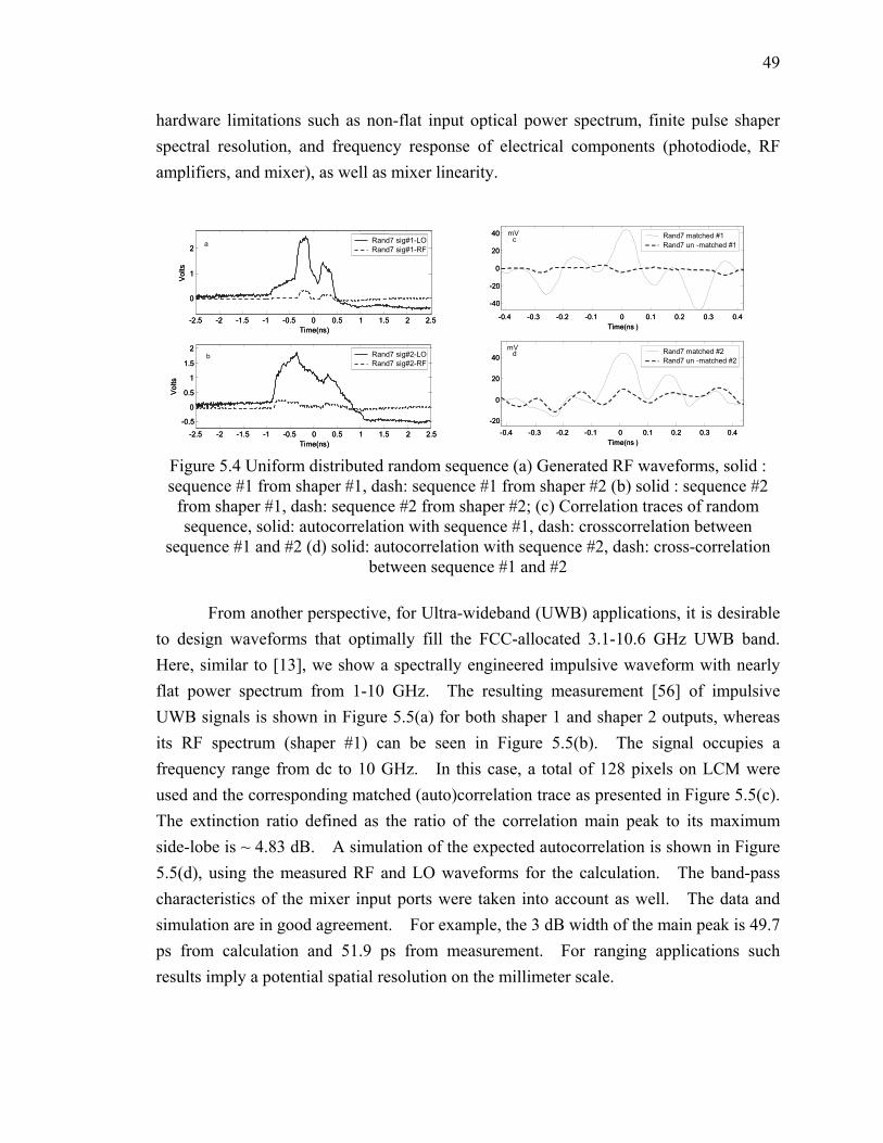
49
hardware limitations such as non-flat input optical power spectrum, finite pulse shaper spectral resolution, and frequency response of electrical components (photodiode, RF amplifiers, and mixer), as well as mixer linearity.
-2.5 -2 -1.5 -1 -0.5 0 0.5 1 1.5 2 2.5
0
1
2
Time(ns)
Vol
ts
Rand7 sig#1-LORand7 sig#1-RF
-2.5 -2 -1.5 -1 -0.5 0 0.5 1 1.5 2 2.5
-0.5
0
0.5
1
1.5
2
Time(ns)
Vol
ts
Rand7 sig#2-LORand7 sig#2-RF
a
b
-2.5 -2 -1.5 -1 -0.5 0 0.5 1 1.5 2 2.5
0
1
2
Time(ns)
Vol
ts
Rand7 sig#1-LORand7 sig#1-RF
-2.5 -2 -1.5 -1 -0.5 0 0.5 1 1.5 2 2.5
-0.5
0
0.5
1
1.5
2
Time(ns)
Vol
ts
Rand7 sig#2-LORand7 sig#2-RF
a
b
Figure 5.4 Uniform distributed random sequence (a) Generated RF waveforms, solid : sequence #1 from shaper #1, dash: sequence #1 from shaper #2 (b) solid : sequence #2
from shaper #1, dash: sequence #2 from shaper #2; (c) Correlation traces of random sequence, solid: autocorrelation with sequence #1, dash: crosscorrelation between
sequence #1 and #2 (d) solid: autocorrelation with sequence #2, dash: cross-correlation between sequence #1 and #2
From another perspective, for Ultra-wideband (UWB) applications, it is desirable to design waveforms that optimally fill the FCC-allocated 3.1-10.6 GHz UWB band. Here, similar to [13], we show a spectrally engineered impulsive waveform with nearly flat power spectrum from 1-10 GHz. The resulting measurement [56] of impulsive UWB signals is shown in Figure 5.5(a) for both shaper 1 and shaper 2 outputs, whereas its RF spectrum (shaper #1) can be seen in Figure 5.5(b). The signal occupies a frequency range from dc to 10 GHz. In this case, a total of 128 pixels on LCM were used and the corresponding matched (auto)correlation trace as presented in Figure 5.5(c). The extinction ratio defined as the ratio of the correlation main peak to its maximum side-lobe is ~ 4.83 dB. A simulation of the expected autocorrelation is shown in Figure 5.5(d), using the measured RF and LO waveforms for the calculation. The band-pass characteristics of the mixer input ports were taken into account as well. The data and simulation are in good agreement. For example, the 3 dB width of the main peak is 49.7 ps from calculation and 51.9 ps from measurement. For ranging applications such results imply a potential spatial resolution on the millimeter scale.
-0.4 -0.3 -0.2 -0.1 0 0.1 0.2 0.3 0.4
-40
-20
0
20
40
Time(ns )
mV Rand7 matched #1Rand7 un - matched #1
-0.4 -0.3 -0.2 -0.1 0 0.1 0.2 0.3 0.4-20
0
20
40
Time(ns )
mVRand7 matched #2Rand7 un - matched #2
a
b
-0.4 -0.3 -0.2 -0.1 0 0.1 0.2 0.3 0.4
-40
-20
0
20
40
Time(ns )
mV Rand7 matched #1Rand7 un - matched #1
-0.4 -0.3 -0.2 -0.1 0 0.1 0.2 0.3 0.4-20
0
20
40
Time(ns )
mV Rand7 matched #2Rand7 un - matched #2
c
d
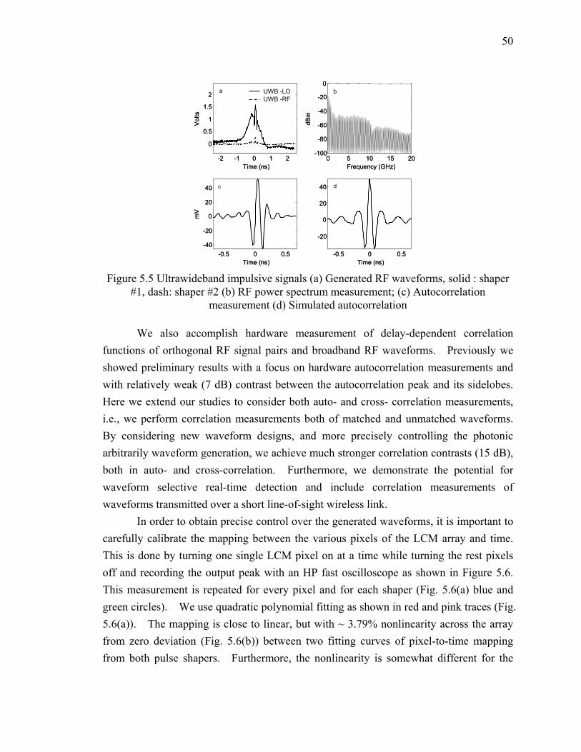
50
-0.5 0 0.5-40
-20
0
20
40
Time (ns)
mV
-2 -1 0 1 2
0
0.5
1
1.5
2
Time (ns)
Vol
ts
UWB -LOUWB -RF
0 5 10 15 20-100
-80
-60
-40
-20
0
Frequency (GHz)
dBm
-0.5 0 0.5
-20
0
20
40
Time (ns)
a b
c d
-0.5 0 0.5-40
-20
0
20
40
Time (ns)
mV
-2 -1 0 1 2
0
0.5
1
1.5
2
Time (ns)
Vol
ts
UWB -LOUWB -RF
0 5 10 15 20-100
-80
-60
-40
-20
0
Frequency (GHz)
dBm
-0.5 0 0.5
-20
0
20
40
Time (ns)
a b
c d
Figure 5.5 Ultrawideband impulsive signals (a) Generated RF waveforms, solid : shaper
#1, dash: shaper #2 (b) RF power spectrum measurement; (c) Autocorrelation measurement (d) Simulated autocorrelation
We also accomplish hardware measurement of delay-dependent correlation functions of orthogonal RF signal pairs and broadband RF waveforms. Previously we showed preliminary results with a focus on hardware autocorrelation measurements and with relatively weak (7 dB) contrast between the autocorrelation peak and its sidelobes. Here we extend our studies to consider both auto- and cross- correlation measurements, i.e., we perform correlation measurements both of matched and unmatched waveforms. By considering new waveform designs, and more precisely controlling the photonic arbitrarily waveform generation, we achieve much stronger correlation contrasts (15 dB), both in auto- and cross-correlation. Furthermore, we demonstrate the potential for waveform selective real-time detection and include correlation measurements of waveforms transmitted over a short line-of-sight wireless link. In order to obtain precise control over the generated waveforms, it is important to carefully calibrate the mapping between the various pixels of the LCM array and time. This is done by turning one single LCM pixel on at a time while turning the rest pixels off and recording the output peak with an HP fast oscilloscope as shown in Figure 5.6. This measurement is repeated for every pixel and for each shaper (Fig. 5.6(a) blue and green circles). We use quadratic polynomial fitting as shown in red and pink traces (Fig. 5.6(a)). The mapping is close to linear, but with ~ 3.79% nonlinearity across the array from zero deviation (Fig. 5.6(b)) between two fitting curves of pixel-to-time mapping from both pulse shapers. Furthermore, the nonlinearity is somewhat different for the
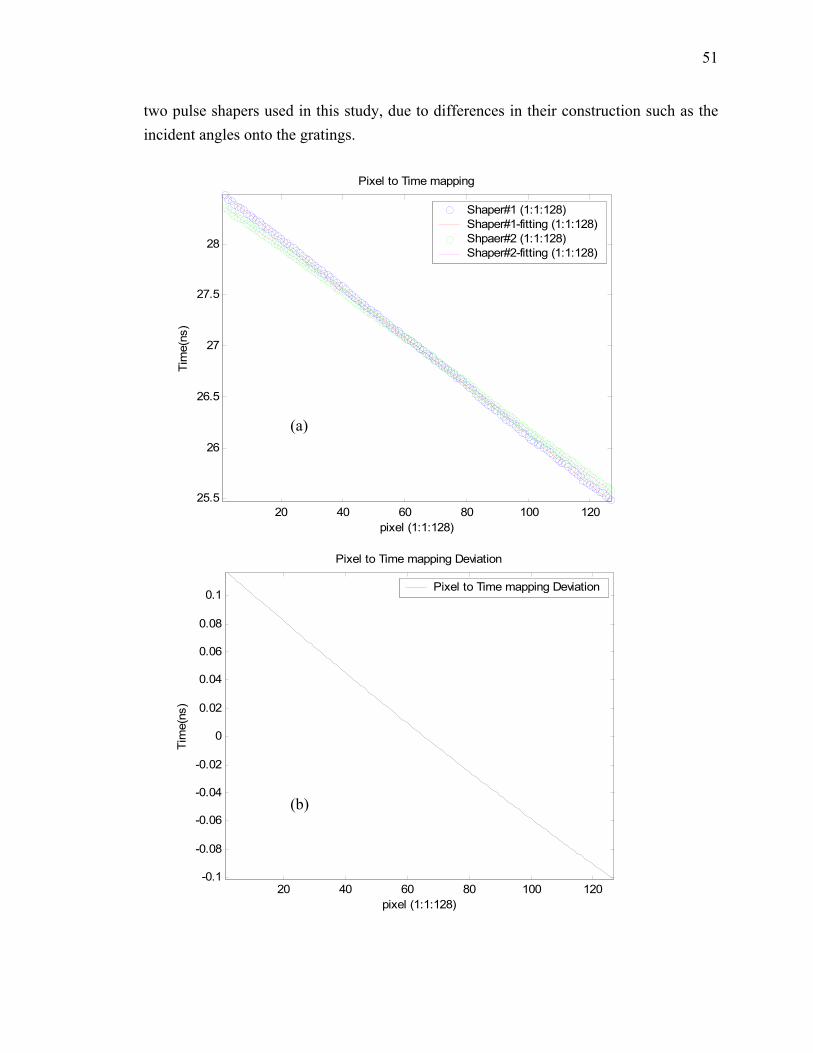
51
two pulse shapers used in this study, due to differences in their construction such as the incident angles onto the gratings.
20 40 60 80 100 12025.5
26
26.5
27
27.5
28
pixel (1:1:128)
Tim
e(ns
)Pixel to Time mapping
Shaper#1 (1:1:128)Shaper#1-fitting (1:1:128)Shpaer#2 (1:1:128)Shaper#2-fitting (1:1:128)
20 40 60 80 100 120-0.1
-0.08
-0.06
-0.04
-0.02
0
0.02
0.04
0.06
0.08
0.1
pixel (1:1:128)
Tim
e(ns
)
Pixel to Time mapping Deviation
Pixel to Time mapping Deviation
(a)
(b)
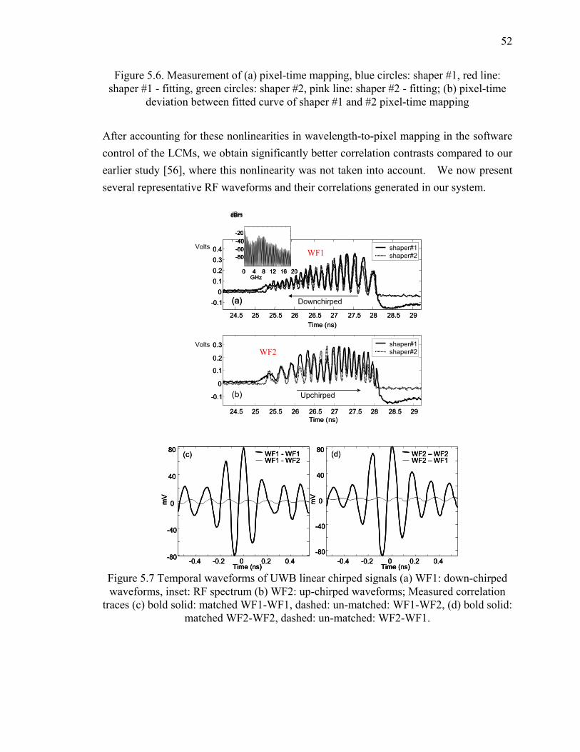
52
Figure 5.6. Measurement of (a) pixel-time mapping, blue circles: shaper #1, red line: shaper #1 - fitting, green circles: shaper #2, pink line: shaper #2 - fitting; (b) pixel-time
deviation between fitted curve of shaper #1 and #2 pixel-time mapping
After accounting for these nonlinearities in wavelength-to-pixel mapping in the software control of the LCMs, we obtain significantly better correlation contrasts compared to our earlier study [56], where this nonlinearity was not taken into account. We now present several representative RF waveforms and their correlations generated in our system.
-0.4 -0.2 0 0.2 0.4-80
-40
0
40
80
Time (ns)
mV
-0.4 -0.2 0 0.2 0.4-80
-40
0
40
80
Time (ns)
mV
WF1 - WF1WF1 - WF2
WF2 – WF2WF2 – WF1
(c) (d)
-0.4 -0.2 0 0.2 0.4-80
-40
0
40
80
Time (ns)
mV
-0.4 -0.2 0 0.2 0.4-80
-40
0
40
80
Time (ns)
mV
WF1 - WF1WF1 - WF2
WF2 – WF2WF2 – WF1
-0.4 -0.2 0 0.2 0.4-80
-40
0
40
80
Time (ns)
mV
-0.4 -0.2 0 0.2 0.4-80
-40
0
40
80
Time (ns)
mV
WF1 - WF1WF1 - WF2
WF2 – WF2WF2 – WF1
(c) (d)
Figure 5.7 Temporal waveforms of UWB linear chirped signals (a) WF1: down-chirped waveforms, inset: RF spectrum (b) WF2: up-chirped waveforms; Measured correlation
traces (c) bold solid: matched WF1-WF1, dashed: un-matched: WF1-WF2, (d) bold solid: matched WF2-WF2, dashed: un-matched: WF2-WF1.
24.5 25 25.5 26 26.5 27 27.5 28 28.5 29 - 0.1
0 0.1 0.2 0.3 0.4
24.5 25 25.5 26 26.5 27 27.5 28 28.5 29 - 0.1
0 0.1 0.2 0.3
Time (ns)
shaper#1 shaper#2
shaper#1 shaper#2
3.29 to 9.83 GHz
(a)
(b)
Time (ns)
GHz0 4 8 12 16 20
-80-60-40-20
dBm
24.5 25 25.5 26 26.5 27 27.5 28 28.5 29 - 0.1
0 0.1 0.2 0.3 0.4 Volts
24.5 25 25.5 26 26.5 27 27.5 28 28.5 29 - 0.1
0 0.1 0.2 0.3
Time (ns)
Volts
shaper#1 shaper#2
shaper#1 shaper#2
Downchirped
Upchirped
(a)
(b)
Time (ns)
GHz0 4 8 12 16 20
-80-60-40-20
dBm
0 4 8 12 16 20
-80-60-40-20
dBm
WF1
WF2
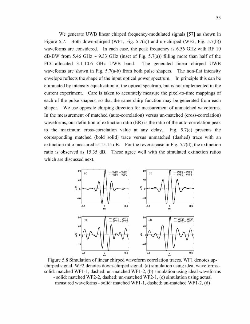
53
We generate UWB linear chirped frequency-modulated signals [57] as shown in Figure 5.7. Both down-chirped (WF1, Fig. 5.7(a)) and up-chirped (WF2, Fig. 5.7(b)) waveforms are considered. In each case, the peak frequency is 6.56 GHz with RF 10 dB-BW from 5.46 GHz ~ 9.33 GHz (inset of Fig. 5.7(a)) filling more than half of the FCC-allocated 3.1-10.6 GHz UWB band. The generated linear chirped UWB waveforms are shown in Fig. 5.7(a-b) from both pulse shapers. The non-flat intensity envelope reflects the shape of the input optical power spectrum. In principle this can be eliminated by intensity equalization of the optical spectrum, but is not implemented in the current experiment. Care is taken to accurately measure the pixel-to-time mappings of each of the pulse shapers, so that the same chirp function may be generated from each shaper. We use opposite chirping direction for measurement of unmatched waveforms. In the measurement of matched (auto-correlation) versus un-matched (cross-correlation) waveforms, our definition of extinction ratio (ER) is the ratio of the auto-correlation peak to the maximum cross-correlation value at any delay. Fig. 5.7(c) presents the corresponding matched (bold solid) trace versus unmatched (dashed) trace with an extinction ratio measured as 15.15 dB. For the reverse case in Fig. 5.7(d), the extinction ratio is observed as 15.35 dB. These agree well with the simulated extinction ratios which are discussed next.
-0.5 0 0.5
-40
0
40
80
ns
WF1 – WF1WF1 – WF2
-0.5 0 0.5
-40
0
40
80
ns
-0.5 0 0.5
-40
0
40
80
ns-0.5 0 0.5
-40
0
40
80
ns
WF2 – WF2WF2 – WF1
WF1 – WF1WF1 – WF2
WF2 – WF2WF2 – WF1
mV
mV
mV
mV
(a) (b)
(c) (d)
-0.5 0 0.5
-40
0
40
80
ns
WF1 – WF1WF1 – WF2
-0.5 0 0.5
-40
0
40
80
ns
-0.5 0 0.5
-40
0
40
80
ns-0.5 0 0.5
-40
0
40
80
ns
WF2 – WF2WF2 – WF1
WF1 – WF1WF1 – WF2
WF2 – WF2WF2 – WF1
mV
mV
mV
mV
(a) (b)
(c) (d)
Figure 5.8 Simulation of linear chirped waveform correlation traces. WF1 denotes up-
chirped signal, WF2 denotes down-chirped signal. (a) simulation using ideal waveforms - solid: matched WF1-1, dashed: un-matched WF1-2, (b) simulation using ideal waveforms
- solid: matched WF2-2, dashed: un-matched WF2-1, (c) simulation using actual measured waveforms - solid: matched WF1-1, dashed: un-matched WF1-2, (d)
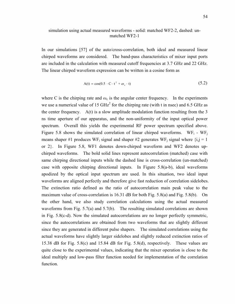
54
simulation using actual measured waveforms - solid: matched WF2-2, dashed: un-matched WF2-1
In our simulations [57] of the auto/cross-correlation, both ideal and measured linear chirped waveforms are considered. The band-pass characteristics of mixer input ports are included in the calculation with measured cutoff frequencies at 3.7 GHz and 22 GHz. The linear chirped waveform expression can be written in a cosine form as
t)+tCcos(0.5A(t) c2 ⋅⋅⋅= ω (5.2)
where C is the chirping rate and ωc is the angular center frequency. In the experiments we use a numerical value of 15 GHz2 for the chirping rate (with t in nsec) and 6.5 GHz as the center frequency. A(t) is a slow amplitude modulation function resulting from the 3 ns time aperture of our apparatus, and the non-uniformity of the input optical power spectrum. Overall this yields the experimental RF power spectrum specified above. Figure 5.8 shows the simulated correlation of linear chirped waveforms. WFi - WFj means shaper #1 produces WFi signal and shaper #2 generates WFj signal where {i,j = 1 or 2}. In Figure 5.8, WF1 denotes down-chirped waveform and WF2 denotes up-chirped waveforms. The bold solid lines represent autocorrelation (matched) case with same chirping directional inputs while the dashed line is cross-correlation (un-matched) case with opposite chirping directional inputs. In Figure 5.8(a-b), ideal waveforms apodized by the optical input spectrum are used. In this situation, two ideal input waveforms are aligned perfectly and therefore give fast reduction of correlation sidelobes. The extinction ratio defined as the ratio of autocorrelation main peak value to the maximum value of cross-correlation is 16.31 dB for both Fig. 5.8(a) and Fig. 5.8(b). On the other hand, we also study correlation calculations using the actual measured waveforms from Fig. 5.7(a) and 5.7(b). The resulting simulated correlations are shown in Fig. 5.8(c-d). Now the simulated autocorrelations are no longer perfectly symmetric, since the autocorrelations are obtained from two waveforms that are slightly different since they are generated in different pulse shapers. The simulated correlations using the actual waveforms have slightly larger sidelobes and slightly reduced extinction ratios of 15.38 dB for Fig. 5.8(c) and 15.84 dB for Fig. 5.8(d), respectively. These values are quite close to the experimental values, indicating that the mixer operation is close to the ideal multiply and low-pass filter function needed for implementation of the correlation function.
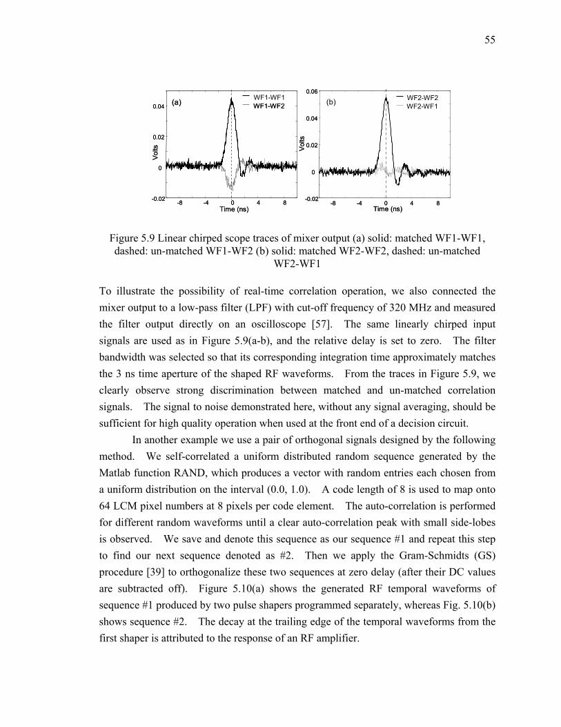
55
-8 -4 0 4 8-0.02
0
0.02
0.04
Time (ns)
WF1-WF1WF1-WF2
-8 -4 0 4 8-0.02
0
0.02
0.04
0.06WF2-WF2WF2-WF1(a) (b)
Time (ns)
Vol
ts Vol
ts
-8 -4 0 4 8-0.02
0
0.02
0.04
Time (ns)
WF1-WF1WF1-WF2
-8 -4 0 4 8-0.02
0
0.02
0.04
0.06WF2-WF2WF2-WF1(a) (b)
Time (ns)
Vol
ts Vol
ts
Figure 5.9 Linear chirped scope traces of mixer output (a) solid: matched WF1-WF1, dashed: un-matched WF1-WF2 (b) solid: matched WF2-WF2, dashed: un-matched
WF2-WF1
To illustrate the possibility of real-time correlation operation, we also connected the mixer output to a low-pass filter (LPF) with cut-off frequency of 320 MHz and measured the filter output directly on an oscilloscope [57]. The same linearly chirped input signals are used as in Figure 5.9(a-b), and the relative delay is set to zero. The filter bandwidth was selected so that its corresponding integration time approximately matches the 3 ns time aperture of the shaped RF waveforms. From the traces in Figure 5.9, we clearly observe strong discrimination between matched and un-matched correlation signals. The signal to noise demonstrated here, without any signal averaging, should be sufficient for high quality operation when used at the front end of a decision circuit. In another example we use a pair of orthogonal signals designed by the following method. We self-correlated a uniform distributed random sequence generated by the Matlab function RAND, which produces a vector with random entries each chosen from a uniform distribution on the interval (0.0, 1.0). A code length of 8 is used to map onto 64 LCM pixel numbers at 8 pixels per code element. The auto-correlation is performed for different random waveforms until a clear auto-correlation peak with small side-lobes is observed. We save and denote this sequence as our sequence #1 and repeat this step to find our next sequence denoted as #2. Then we apply the Gram-Schmidts (GS) procedure [39] to orthogonalize these two sequences at zero delay (after their DC values are subtracted off). Figure 5.10(a) shows the generated RF temporal waveforms of sequence #1 produced by two pulse shapers programmed separately, whereas Fig. 5.10(b) shows sequence #2. The decay at the trailing edge of the temporal waveforms from the first shaper is attributed to the response of an RF amplifier.
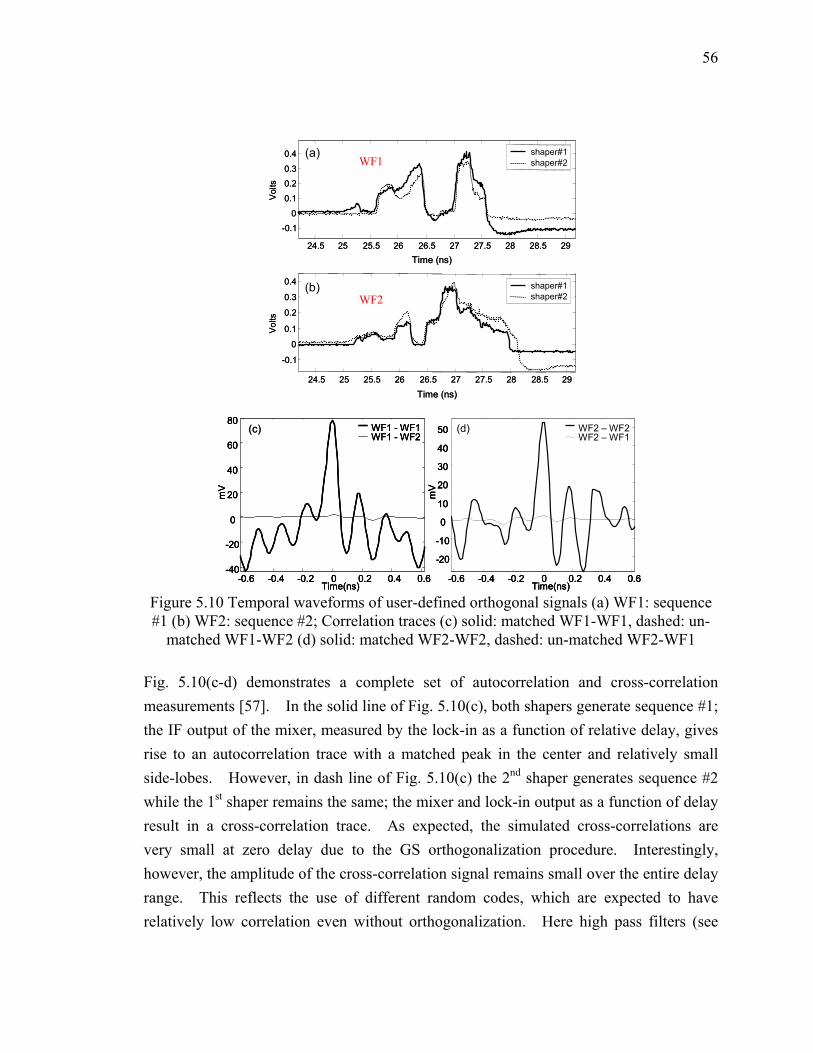
56
24.5 25 25.5 26 26.5 27 27.5 28 28.5 29
-0.1
0
0.1
0.2
0.3
0.4
Vol
ts
shaper#1shaper#2
24.5 25 25.5 26 26.5 27 27.5 28 28.5 29
-0.1
0
0.1
0.2
0.3
0.4V
olts
shaper#1shaper#2
(a)
(b)
Time (ns)
Time (ns)
24.5 25 25.5 26 26.5 27 27.5 28 28.5 29
-0.1
0
0.1
0.2
0.3
0.4
Vol
ts
shaper#1shaper#2
24.5 25 25.5 26 26.5 27 27.5 28 28.5 29
-0.1
0
0.1
0.2
0.3
0.4V
olts
shaper#1shaper#2
(a)
(b)
Time (ns)
Time (ns)
-0.6 -0.4 -0.2 0 0.2 0.4 0.6-40
-20
0
20
40
60
80
Time(ns)
mV
WF1 - WF1WF1 - WF2
-0.6 -0.4 -0.2 0 0.2 0.4 0.6
-20
-10
0
10
20
30
40
50
Time(ns)
mV
WF2 – WF2WF2 – WF1
(c) (d)
-0.6 -0.4 -0.2 0 0.2 0.4 0.6-40
-20
0
20
40
60
80
Time(ns)
mV
WF1 - WF1WF1 - WF2
-0.6 -0.4 -0.2 0 0.2 0.4 0.6
-20
-10
0
10
20
30
40
50
Time(ns)
mV
WF2 – WF2WF2 – WF1
-0.6 -0.4 -0.2 0 0.2 0.4 0.6-40
-20
0
20
40
60
80
Time(ns)
mV
WF1 - WF1WF1 - WF2
-0.6 -0.4 -0.2 0 0.2 0.4 0.6
-20
-10
0
10
20
30
40
50
Time(ns)
mV
WF2 – WF2WF2 – WF1
(c) (d)
Figure 5.10 Temporal waveforms of user-defined orthogonal signals (a) WF1: sequence #1 (b) WF2: sequence #2; Correlation traces (c) solid: matched WF1-WF1, dashed: un-
matched WF1-WF2 (d) solid: matched WF2-WF2, dashed: un-matched WF2-WF1 Fig. 5.10(c-d) demonstrates a complete set of autocorrelation and cross-correlation measurements [57]. In the solid line of Fig. 5.10(c), both shapers generate sequence #1; the IF output of the mixer, measured by the lock-in as a function of relative delay, gives rise to an autocorrelation trace with a matched peak in the center and relatively small side-lobes. However, in dash line of Fig. 5.10(c) the 2nd shaper generates sequence #2 while the 1st shaper remains the same; the mixer and lock-in output as a function of delay result in a cross-correlation trace. As expected, the simulated cross-correlations are very small at zero delay due to the GS orthogonalization procedure. Interestingly, however, the amplitude of the cross-correlation signal remains small over the entire delay range. This reflects the use of different random codes, which are expected to have relatively low correlation even without orthogonalization. Here high pass filters (see
WF1
WF2
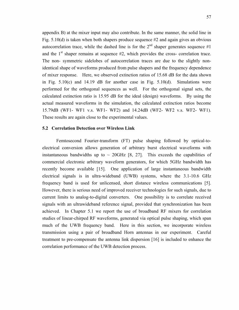
57
appendix B) at the mixer input may also contribute. In the same manner, the solid line in Fig. 5.10(d) is taken when both shapers produce sequence #2 and again gives an obvious autocorrelation trace, while the dashed line is for the 2nd shaper generates sequence #1 and the 1st shaper remains at sequence #2, which provides the cross- correlation trace. The non- symmetric sidelobes of autocorrelation traces are due to the slightly non-identical shape of waveforms produced from pulse shapers and the frequency dependence of mixer response. Here, we observed extinction ratios of 15.68 dB for the data shown in Fig. 5.10(c) and 14.19 dB for another case in Fig. 5.10(d). Simulations were performed for the orthogonal sequences as well. For the orthogonal signal sets, the calculated extinction ratio is 15.95 dB for the ideal (design) waveforms. By using the actual measured waveforms in the simulation, the calculated extinction ratios become 15.79dB (WF1- WF1 v.s. WF1- WF2) and 14.24dB (WF2- WF2 v.s. WF2- WF1). These results are again close to the experimental values. 5.2 Correlation Detection over Wireless Link
Femtosecond Fourier-transform (FT) pulse shaping followed by optical-to-electrical conversion allows generation of arbitrary burst electrical waveforms with instantaneous bandwidths up to ~ 20GHz [8, 27]. This exceeds the capabilities of commercial electronic arbitrary waveform generators, for which 5GHz bandwidth has recently become available [15]. One application of large instantaneous bandwidth electrical signals is in ultra-wideband (UWB) systems, where the 3.1-10.6 GHz frequency band is used for unlicensed, short distance wireless communications [5]. However, there is serious need of improved receiver technologies for such signals, due to current limits to analog-to-digital converters. One possibility is to correlate received signals with an ultrawideband reference signal, provided that synchronization has been achieved. In Chapter 5.1 we report the use of broadband RF mixers for correlation studies of linear-chirped RF waveforms, generated via optical pulse shaping, which span much of the UWB frequency band. Here in this section, we incorporate wireless transmission using a pair of broadband Horn antennas in our experiment. Careful treatment to pre-compensate the antenna link dispersion [16] is included to enhance the correlation performance of the UWB detection process.
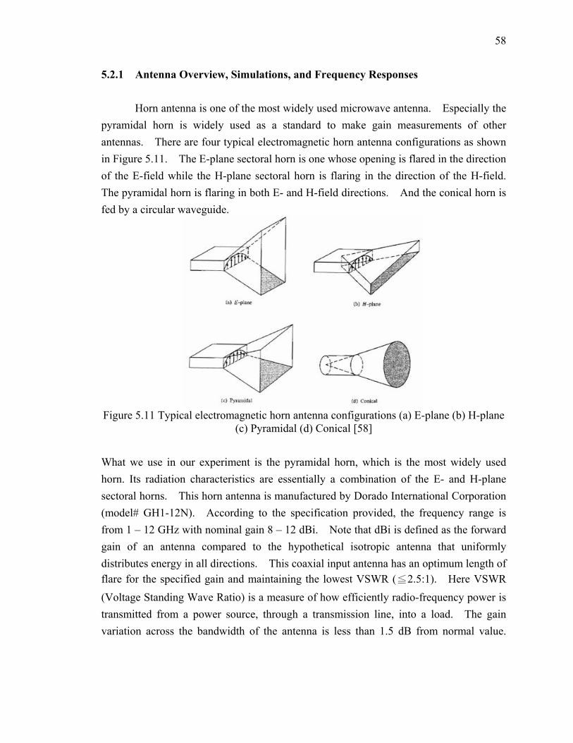
58
5.2.1 Antenna Overview, Simulations, and Frequency Responses Horn antenna is one of the most widely used microwave antenna. Especially the pyramidal horn is widely used as a standard to make gain measurements of other antennas. There are four typical electromagnetic horn antenna configurations as shown in Figure 5.11. The E-plane sectoral horn is one whose opening is flared in the direction of the E-field while the H-plane sectoral horn is flaring in the direction of the H-field. The pyramidal horn is flaring in both E- and H-field directions. And the conical horn is fed by a circular waveguide.
Figure 5.11 Typical electromagnetic horn antenna configurations (a) E-plane (b) H-plane
(c) Pyramidal (d) Conical [58]
What we use in our experiment is the pyramidal horn, which is the most widely used horn. Its radiation characteristics are essentially a combination of the E- and H-plane sectoral horns. This horn antenna is manufactured by Dorado International Corporation (model# GH1-12N). According to the specification provided, the frequency range is from 1 – 12 GHz with nominal gain 8 – 12 dBi. Note that dBi is defined as the forward gain of an antenna compared to the hypothetical isotropic antenna that uniformly distributes energy in all directions. This coaxial input antenna has an optimum length of flare for the specified gain and maintaining the lowest VSWR (≦2.5:1). Here VSWR (Voltage Standing Wave Ratio) is a measure of how efficiently radio-frequency power is transmitted from a power source, through a transmission line, into a load. The gain variation across the bandwidth of the antenna is less than 1.5 dB from normal value.
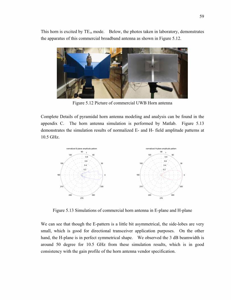
59
This horn is excited by TE10 mode. Below, the photos taken in laboratory, demonstrates the apparatus of this commercial broadband antenna as shown in Figure 5.12.
Figure 5.12 Picture of commercial UWB Horn antenna
Complete Details of pyramidal horn antenna modeling and analysis can be found in the appendix C. The horn antenna simulation is performed by Matlab. Figure 5.13 demonstrates the simulation results of normalized E- and H- field amplitude patterns at 10.5 GHz.
0.2
0.4
0.6
0.8
1
30
210
60
240
90
270
120
300
150
330
180 0
normalized E-plane amplitude pattern
0.2
0.4
0.6
0.8
1
30
210
60
240
90
270
120
300
150
330
180 0
normalized H-plane amplitude pattern
Figure 5.13 Simulations of commercial horn antenna in E-plane and H-plane
We can see that though the E-pattern is a little bit asymmetrical, the side-lobes are very small, which is good for directional transceiver application purposes. On the other hand, the H-plane is in perfect symmetrical shape. We observed the 3 dB beamwidth is around 50 degree for 10.5 GHz from these simulation results, which is in good consistency with the gain profile of the horn antenna vendor specification.
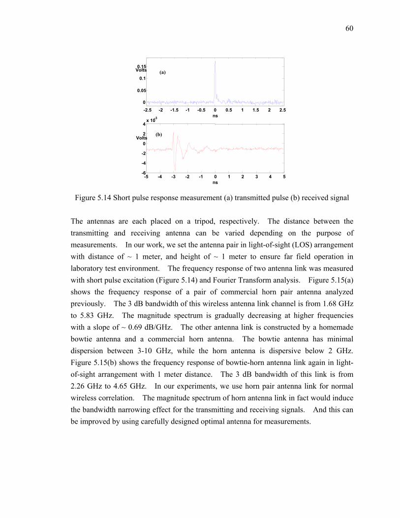
60
Figure 5.14 Short pulse response measurement (a) transmitted pulse (b) received signal
The antennas are each placed on a tripod, respectively. The distance between the transmitting and receiving antenna can be varied depending on the purpose of measurements. In our work, we set the antenna pair in light-of-sight (LOS) arrangement with distance of ~ 1 meter, and height of ~ 1 meter to ensure far field operation in laboratory test environment. The frequency response of two antenna link was measured with short pulse excitation (Figure 5.14) and Fourier Transform analysis. Figure 5.15(a) shows the frequency response of a pair of commercial horn pair antenna analyzed previously. The 3 dB bandwidth of this wireless antenna link channel is from 1.68 GHz to 5.83 GHz. The magnitude spectrum is gradually decreasing at higher frequencies with a slope of ~ 0.69 dB/GHz. The other antenna link is constructed by a homemade bowtie antenna and a commercial horn antenna. The bowtie antenna has minimal dispersion between 3-10 GHz, while the horn antenna is dispersive below 2 GHz. Figure 5.15(b) shows the frequency response of bowtie-horn antenna link again in light-of-sight arrangement with 1 meter distance. The 3 dB bandwidth of this link is from 2.26 GHz to 4.65 GHz. In our experiments, we use horn pair antenna link for normal wireless correlation. The magnitude spectrum of horn antenna link in fact would induce the bandwidth narrowing effect for the transmitting and receiving signals. And this can be improved by using carefully designed optimal antenna for measurements.
-5 -4 -3 -2 -1 0 1 2 3 4 5 -6 -4 -2 0 2 4 x 10 -3
ns
Volts
-2.5 -2 -1.5 -1 -0.5 0 0.5 1 1.5 2 2.5 0
0.05 0.1
0.15
ns
Volts (a)
(b)
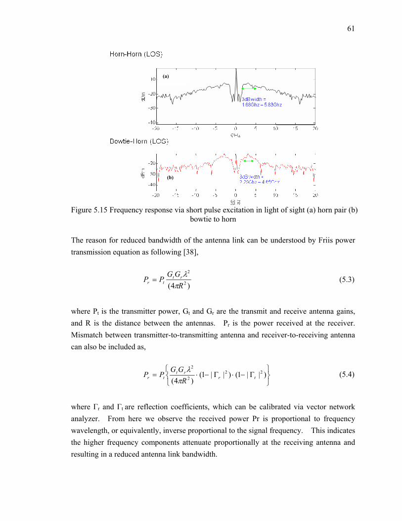
61
Figure 5.15 Frequency response via short pulse excitation in light of sight (a) horn pair (b)
bowtie to horn The reason for reduced bandwidth of the antenna link can be understood by Friis power transmission equation as following [38],
)4( 2
2
RGG
PP rttr π
λ=
(5.3)
where Pt is the transmitter power, Gt and Gr are the transmit and receive antenna gains, and R is the distance between the antennas. Pr is the power received at the receiver. Mismatch between transmitter-to-transmitting antenna and receiver-to-receiving antenna can also be included as,
Γ−⋅Γ−⋅= )||1()||1()4(
222
2
trrt
tr RGG
PPπ
λ (5.4)
where Γr and Γt are reflection coefficients, which can be calibrated via vector network analyzer. From here we observe the received power Pr is proportional to frequency wavelength, or equivalently, inverse proportional to the signal frequency. This indicates the higher frequency components attenuate proportionally at the receiving antenna and resulting in a reduced antenna link bandwidth.
(a)
(b)
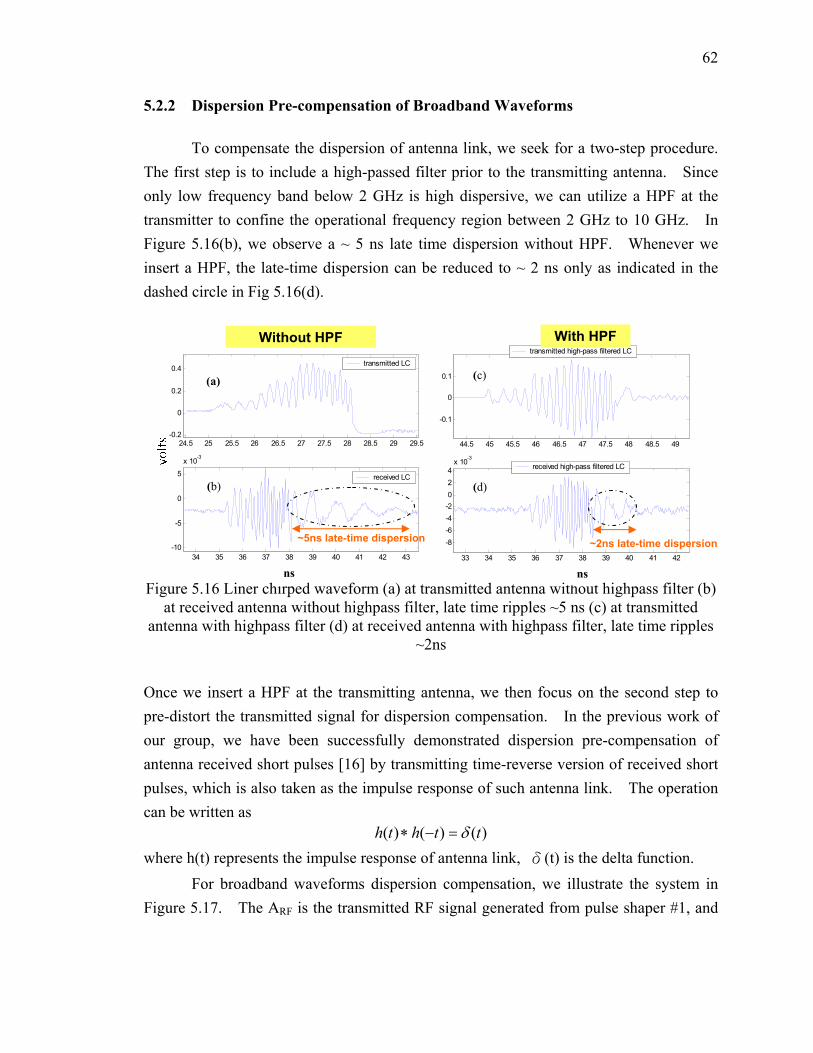
62
5.2.2 Dispersion Pre-compensation of Broadband Waveforms To compensate the dispersion of antenna link, we seek for a two-step procedure. The first step is to include a high-passed filter prior to the transmitting antenna. Since only low frequency band below 2 GHz is high dispersive, we can utilize a HPF at the transmitter to confine the operational frequency region between 2 GHz to 10 GHz. In Figure 5.16(b), we observe a ~ 5 ns late time dispersion without HPF. Whenever we insert a HPF, the late-time dispersion can be reduced to ~ 2 ns only as indicated in the dashed circle in Fig 5.16(d).
Figure 5.16 Liner chirped waveform (a) at transmitted antenna without highpass filter (b)
at received antenna without highpass filter, late time ripples ~5 ns (c) at transmitted antenna with highpass filter (d) at received antenna with highpass filter, late time ripples
~2ns Once we insert a HPF at the transmitting antenna, we then focus on the second step to pre-distort the transmitted signal for dispersion compensation. In the previous work of our group, we have been successfully demonstrated dispersion pre-compensation of antenna received short pulses [16] by transmitting time-reverse version of received short pulses, which is also taken as the impulse response of such antenna link. The operation can be written as
)()()( tthth δ=−∗ where h(t) represents the impulse response of antenna link, δ(t) is the delta function. For broadband waveforms dispersion compensation, we illustrate the system in Figure 5.17. The ARF is the transmitted RF signal generated from pulse shaper #1, and
24.5 25 25.5 26 26.5 27 27.5 28 28.5 29 29.5-0.2
0
0.2
0.4
34 35 36 37 38 39 40 41 42 43-10
-5
0
5
x 10-3
received LC
transmitted LC
44.5 45 45.5 46 46.5 47 47.5 48 48.5 49
-0.1
0
0.1
33 34 35 36 37 38 39 40 41 42
-8-6-4-2024
x 10-3
received high-pass filtered LC
transmitted high-pass filtered LC
~5ns late-time dispersion ~2ns late-time dispersion
Without HPF With HPF
(a) (a)
(b)
(c)
(d)
ns ns
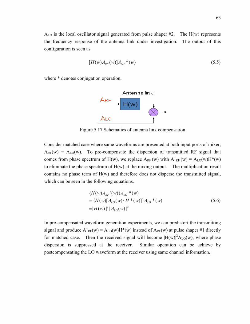
63
ALO is the local oscillator signal generated from pulse shaper #2. The H(w) represents the frequency response of the antenna link under investigation. The output of this configuration is seen as
)(*)]()([ wAwAwH LORF (5.5)
where * denotes conjugation operation.
Figure 5.17 Schematics of antenna link compensation
Consider matched case where same waveforms are presented at both input ports of mixer, ARF(w) = ALO(w). To pre-compensate the dispersion of transmitted RF signal that comes from phase spectrum of H(w), we replace ARF (w) with A’RF (w) = ALO(w)H*(w) to eliminate the phase spectrum of H(w) at the mixing output. The multiplication result contains no phase term of H(w) and therefore does not disperse the transmitted signal, which can be seen in the following equations.
22 |)(||)(|
)(*)]}(*)()[({)(*)}(')({
wAwH
wAwHwAwHwAwAwH
LO
LOLO
LORF
=
⋅=
(5.6)
In pre-compensated waveform generation experiments, we can predistort the transmitting signal and produce A’RF(w) = ALO(w)H*(w) instead of ARF(w) at pulse shaper #1 directly for matched case. Then the received signal will become |H(w)|2ALO(w), where phase dispersion is suppressed at the receiver. Similar operation can be achieve by postcompensating the LO waveform at the receiver using same channel information.
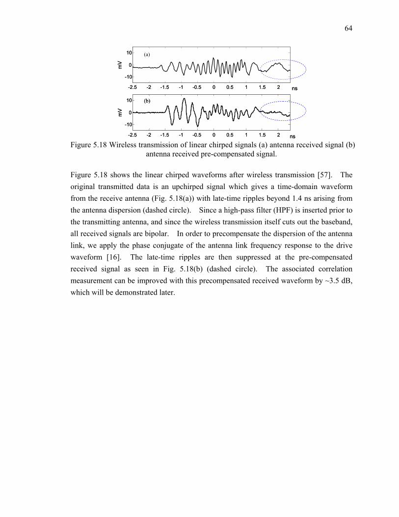
64
-2.5 -2 -1.5 -1 -0.5 0 0.5 1 1.5 2
-10
0
10
ns
mV
-2.5 -2 -1.5 -1 -0.5 0 0.5 1 1.5 2
-10
0
10
ns
mV
(b)
(a)
-2.5 -2 -1.5 -1 -0.5 0 0.5 1 1.5 2
-10
0
10
ns
mV
-2.5 -2 -1.5 -1 -0.5 0 0.5 1 1.5 2
-10
0
10
ns
mV
(b)
(a)
Figure 5.18 Wireless transmission of linear chirped signals (a) antenna received signal (b)
antenna received pre-compensated signal. Figure 5.18 shows the linear chirped waveforms after wireless transmission [57]. The original transmitted data is an upchirped signal which gives a time-domain waveform from the receive antenna (Fig. 5.18(a)) with late-time ripples beyond 1.4 ns arising from the antenna dispersion (dashed circle). Since a high-pass filter (HPF) is inserted prior to the transmitting antenna, and since the wireless transmission itself cuts out the baseband, all received signals are bipolar. In order to precompensate the dispersion of the antenna link, we apply the phase conjugate of the antenna link frequency response to the drive waveform [16]. The late-time ripples are then suppressed at the pre-compensated received signal as seen in Fig. 5.18(b) (dashed circle). The associated correlation measurement can be improved with this precompensated received waveform by ~3.5 dB, which will be demonstrated later.
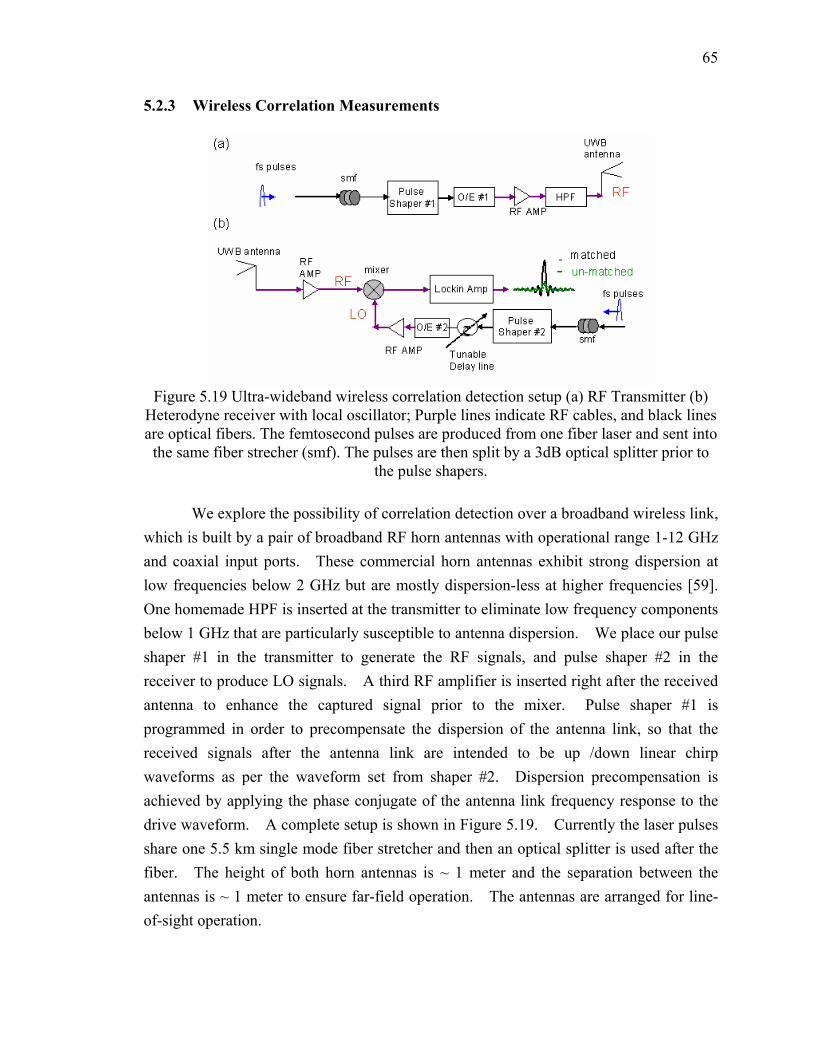
65
5.2.3 Wireless Correlation Measurements
Figure 5.19 Ultra-wideband wireless correlation detection setup (a) RF Transmitter (b)
Heterodyne receiver with local oscillator; Purple lines indicate RF cables, and black lines are optical fibers. The femtosecond pulses are produced from one fiber laser and sent into
the same fiber strecher (smf). The pulses are then split by a 3dB optical splitter prior to the pulse shapers.
We explore the possibility of correlation detection over a broadband wireless link, which is built by a pair of broadband RF horn antennas with operational range 1-12 GHz and coaxial input ports. These commercial horn antennas exhibit strong dispersion at low frequencies below 2 GHz but are mostly dispersion-less at higher frequencies [59]. One homemade HPF is inserted at the transmitter to eliminate low frequency components below 1 GHz that are particularly susceptible to antenna dispersion. We place our pulse shaper #1 in the transmitter to generate the RF signals, and pulse shaper #2 in the receiver to produce LO signals. A third RF amplifier is inserted right after the received antenna to enhance the captured signal prior to the mixer. Pulse shaper #1 is programmed in order to precompensate the dispersion of the antenna link, so that the received signals after the antenna link are intended to be up /down linear chirp waveforms as per the waveform set from shaper #2. Dispersion precompensation is achieved by applying the phase conjugate of the antenna link frequency response to the drive waveform. A complete setup is shown in Figure 5.19. Currently the laser pulses share one 5.5 km single mode fiber stretcher and then an optical splitter is used after the fiber. The height of both horn antennas is ~ 1 meter and the separation between the antennas is ~ 1 meter to ensure far-field operation. The antennas are arranged for line-of-sight operation.
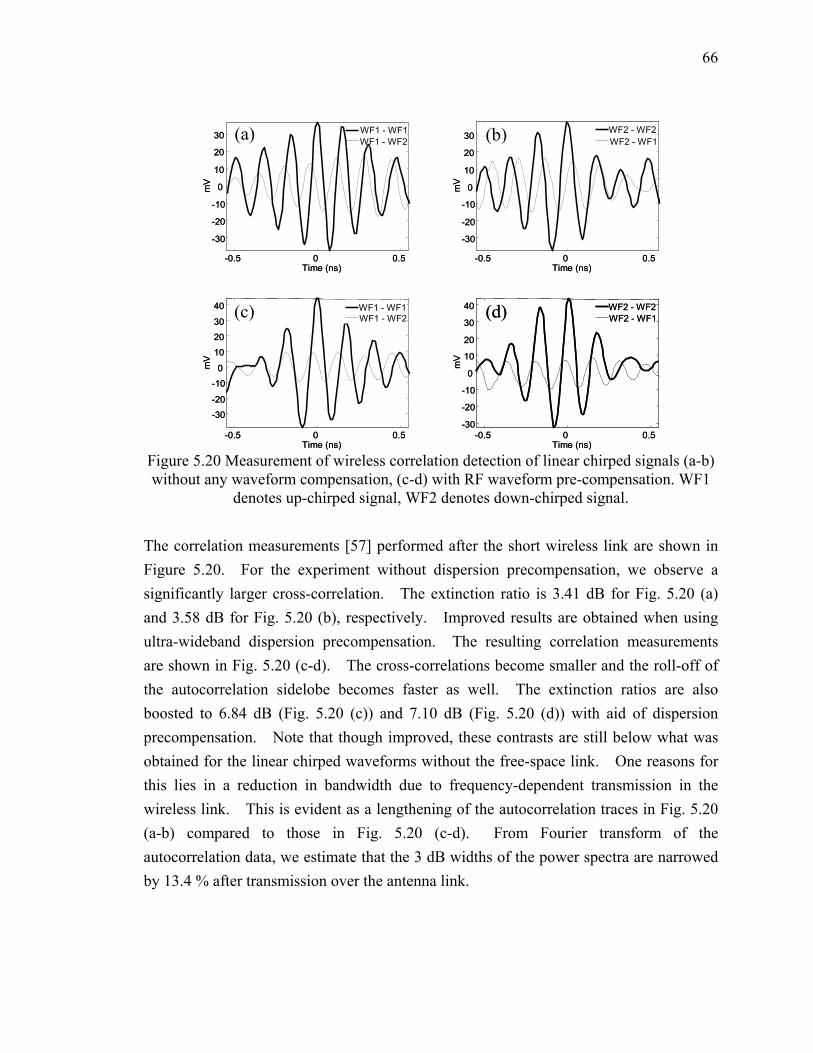
66
-0.5 0 0.5
-30
-20
-10
0
10
20
30
Time (ns)
mV
WF1 - WF1WF1 - WF2
-0.5 0 0.5
-30
-20
-10
0
10
20
30
Time (ns)
mV
WF2 - WF2WF2 - WF1
-0.5 0 0.5
-30
-20
-10
0
10
20
30
40
Time (ns)
mV
WF1 - WF1WF1 - WF2
-0.5 0 0.5-30
-20
-10
0
10
20
30
40
Time (ns)m
V
WF2 - WF2WF2 - WF1
(b)(a)
(c) (d)
-0.5 0 0.5
-30
-20
-10
0
10
20
30
Time (ns)
mV
WF1 - WF1WF1 - WF2
-0.5 0 0.5
-30
-20
-10
0
10
20
30
Time (ns)
mV
WF2 - WF2WF2 - WF1
-0.5 0 0.5
-30
-20
-10
0
10
20
30
40
Time (ns)
mV
WF1 - WF1WF1 - WF2
-0.5 0 0.5-30
-20
-10
0
10
20
30
40
Time (ns)m
V
WF2 - WF2WF2 - WF1
(b)(a)
(c) (d)
Figure 5.20 Measurement of wireless correlation detection of linear chirped signals (a-b) without any waveform compensation, (c-d) with RF waveform pre-compensation. WF1
denotes up-chirped signal, WF2 denotes down-chirped signal. The correlation measurements [57] performed after the short wireless link are shown in Figure 5.20. For the experiment without dispersion precompensation, we observe a significantly larger cross-correlation. The extinction ratio is 3.41 dB for Fig. 5.20 (a) and 3.58 dB for Fig. 5.20 (b), respectively. Improved results are obtained when using ultra-wideband dispersion precompensation. The resulting correlation measurements are shown in Fig. 5.20 (c-d). The cross-correlations become smaller and the roll-off of the autocorrelation sidelobe becomes faster as well. The extinction ratios are also boosted to 6.84 dB (Fig. 5.20 (c)) and 7.10 dB (Fig. 5.20 (d)) with aid of dispersion precompensation. Note that though improved, these contrasts are still below what was obtained for the linear chirped waveforms without the free-space link. One reasons for this lies in a reduction in bandwidth due to frequency-dependent transmission in the wireless link. This is evident as a lengthening of the autocorrelation traces in Fig. 5.20 (a-b) compared to those in Fig. 5.20 (c-d). From Fourier transform of the autocorrelation data, we estimate that the 3 dB widths of the power spectra are narrowed by 13.4 % after transmission over the antenna link.
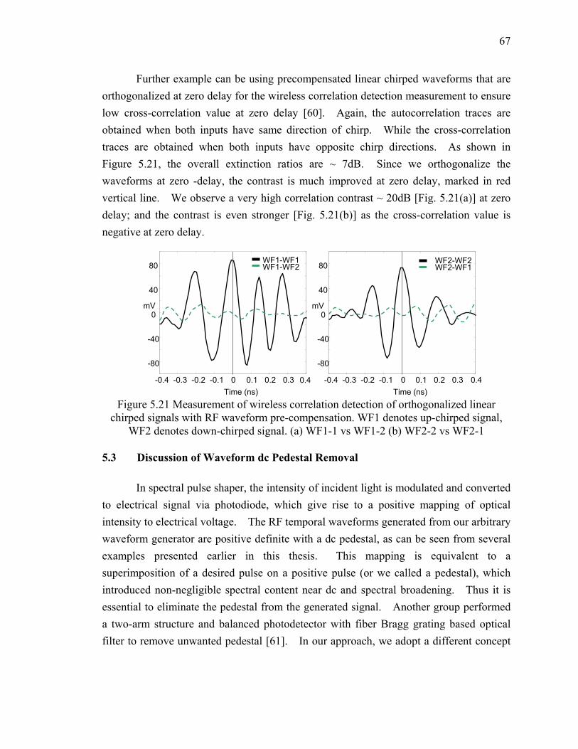
67
Further example can be using precompensated linear chirped waveforms that are orthogonalized at zero delay for the wireless correlation detection measurement to ensure low cross-correlation value at zero delay [60]. Again, the autocorrelation traces are obtained when both inputs have same direction of chirp. While the cross-correlation traces are obtained when both inputs have opposite chirp directions. As shown in Figure 5.21, the overall extinction ratios are ~ 7dB. Since we orthogonalize the waveforms at zero -delay, the contrast is much improved at zero delay, marked in red vertical line. We observe a very high correlation contrast ~ 20dB [Fig. 5.21(a)] at zero delay; and the contrast is even stronger [Fig. 5.21(b)] as the cross-correlation value is negative at zero delay.
Figure 5.21 Measurement of wireless correlation detection of orthogonalized linear
chirped signals with RF waveform pre-compensation. WF1 denotes up-chirped signal, WF2 denotes down-chirped signal. (a) WF1-1 vs WF1-2 (b) WF2-2 vs WF2-1
5.3 Discussion of Waveform dc Pedestal Removal In spectral pulse shaper, the intensity of incident light is modulated and converted to electrical signal via photodiode, which give rise to a positive mapping of optical intensity to electrical voltage. The RF temporal waveforms generated from our arbitrary waveform generator are positive definite with a dc pedestal, as can be seen from several examples presented earlier in this thesis. This mapping is equivalent to a superimposition of a desired pulse on a positive pulse (or we called a pedestal), which introduced non-negligible spectral content near dc and spectral broadening. Thus it is essential to eliminate the pedestal from the generated signal. Another group performed a two-arm structure and balanced photodetector with fiber Bragg grating based optical filter to remove unwanted pedestal [61]. In our approach, we adopt a different concept
0.4-0.4 -0.3 -0.2 -0.1 0 0.1 0.2 0.3
-80
-40
0
40
80
Time (ns)
WF1-WF1WF1-WF2
-0.4 -0.3 -0.2 -0.1 0 0.1 0.2 0.3 0.4
-80
-40
0
40
80
Time (ns)
mV
WF2-WF2WF2-WF1
mV
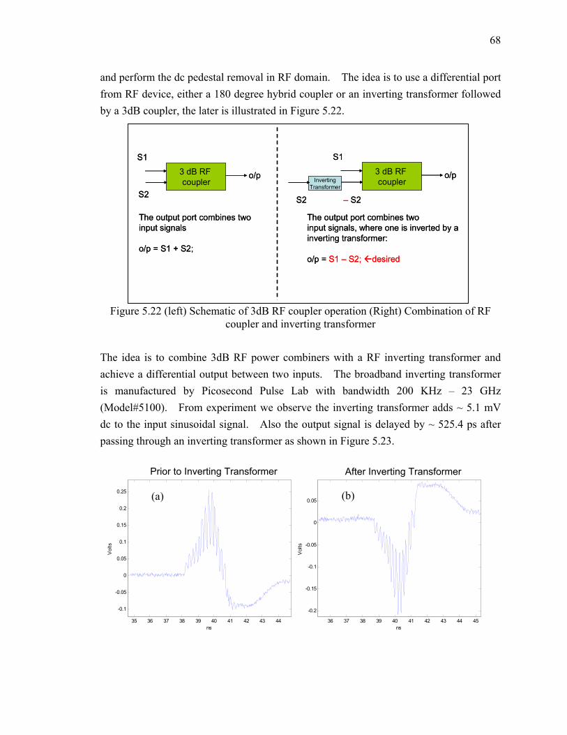
68
and perform the dc pedestal removal in RF domain. The idea is to use a differential port from RF device, either a 180 degree hybrid coupler or an inverting transformer followed by a 3dB coupler, the later is illustrated in Figure 5.22.
Figure 5.22 (left) Schematic of 3dB RF coupler operation (Right) Combination of RF
coupler and inverting transformer The idea is to combine 3dB RF power combiners with a RF inverting transformer and achieve a differential output between two inputs. The broadband inverting transformer is manufactured by Picosecond Pulse Lab with bandwidth 200 KHz – 23 GHz (Model#5100). From experiment we observe the inverting transformer adds ~ 5.1 mV dc to the input sinusoidal signal. Also the output signal is delayed by ~ 525.4 ps after passing through an inverting transformer as shown in Figure 5.23.
35 36 37 38 39 40 41 42 43 44
-0.1
-0.05
0
0.05
0.1
0.15
0.2
0.25
ns
Vol
ts
Prior to Inverting Transformer After Inverting Transformer
36 37 38 39 40 41 42 43 44 45
-0.2
-0.15
-0.1
-0.05
0
0.05
ns
Vol
ts
(a) (b)
3 dB RF coupler
S1
S2
o/p
The output port combines two input signals
o/p = S1 + S2;
3 dB RF coupler
S1
– S2
o/pInverting
Transformer
S2
The output port combines two input signals, where one is inverted by ainverting transformer:
o/p = S1 – S2; desired
3 dB RF coupler
S1
S2
o/p
The output port combines two input signals
o/p = S1 + S2;
3 dB RF coupler
S1
– S2
o/pInverting
Transformer
S2
The output port combines two input signals, where one is inverted by ainverting transformer:
o/p = S1 – S2; desired
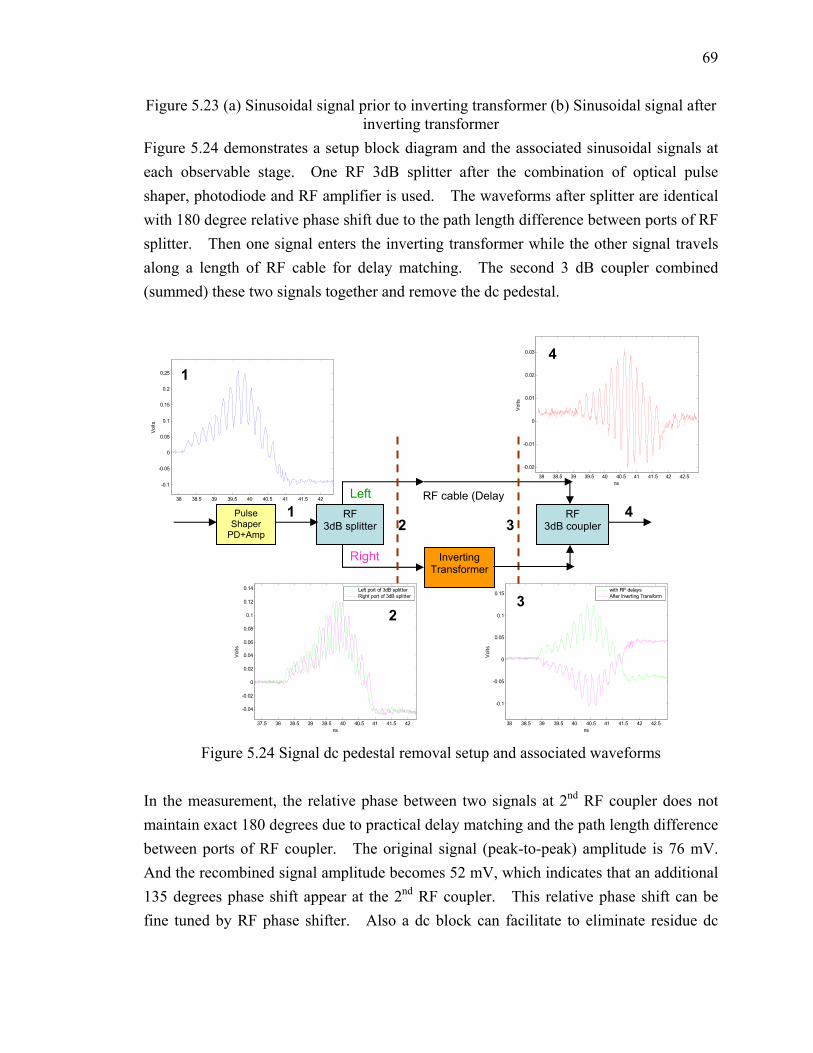
69
Figure 5.23 (a) Sinusoidal signal prior to inverting transformer (b) Sinusoidal signal after inverting transformer
Figure 5.24 demonstrates a setup block diagram and the associated sinusoidal signals at each observable stage. One RF 3dB splitter after the combination of optical pulse shaper, photodiode and RF amplifier is used. The waveforms after splitter are identical with 180 degree relative phase shift due to the path length difference between ports of RF splitter. Then one signal enters the inverting transformer while the other signal travels along a length of RF cable for delay matching. The second 3 dB coupler combined (summed) these two signals together and remove the dc pedestal.
Figure 5.24 Signal dc pedestal removal setup and associated waveforms
In the measurement, the relative phase between two signals at 2nd RF coupler does not maintain exact 180 degrees due to practical delay matching and the path length difference between ports of RF coupler. The original signal (peak-to-peak) amplitude is 76 mV. And the recombined signal amplitude becomes 52 mV, which indicates that an additional 135 degrees phase shift appear at the 2nd RF coupler. This relative phase shift can be fine tuned by RF phase shifter. Also a dc block can facilitate to eliminate residue dc
38 38.5 39 39.5 40 40.5 41 41.5 42
-0.1
-0.05
0
0.05
0.1
0.15
0.2
0.25
ns
Vol
ts
Pulse Shaper
PD+Amp
RF 3dB splitter
RF 3dB coupler
Inverting Transformer
RF cable (Delay
38 38.5 39 39.5 40 40.5 41 41.5 42 42.5
-0.02
-0.01
0
0.01
0.02
0.03
ns
Vol
ts
37.5 38 38.5 39 39.5 40 40.5 41 41.5 42
-0.04
-0.02
0
0.02
0.04
0.06
0.08
0.1
0.12
0.14
ns
Vol
ts
Left port of 3dB splitterRight port of 3dB splitter
38 38.5 39 39.5 40 40.5 41 41.5 42 42.5
-0.1
-0.05
0
0.05
0.1
0.15
ns
Vol
ts
with RF delaysAfter Inverting Transform
1 2 3
4
1
23
4
Left
Right
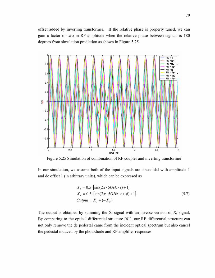
70
offset added by inverting transformer. If the relative phase is properly tuned, we can gain a factor of two in RF amplitude when the relative phase between signals is 180 degrees from simulation prediction as shown in Figure 5.25.
Figure 5.25 Simulation of combination of RF coupler and inverting transformer
In our simulation, we assume both of the input signals are sinusoidal with amplitude 1 and dc offset 1 (in arbitrary units), which can be expressed as
[ ][ ]
)(1)52sin(5.0
1)52sin(5.0
rl
r
l
XXOutputtGHzXtGHzX
−+=++⋅⋅⋅=
+⋅⋅⋅=φπ
π (5.7)
The output is obtained by summing the Xl signal with an inverse version of Xr signal. By comparing to the optical differential structure [61], our RF differential structure can not only remove the dc pedestal came from the incident optical spectrum but also cancel the pedestal induced by the photodiode and RF amplifier responses.
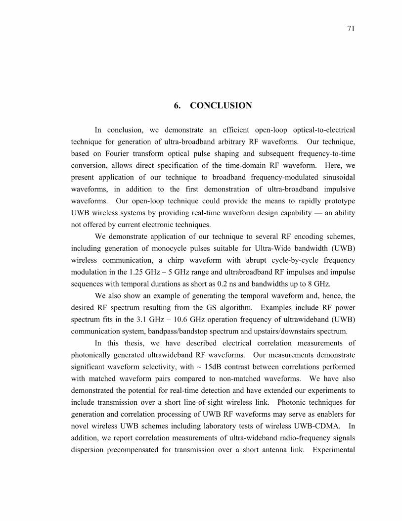
71
6. CONCLUSION In conclusion, we demonstrate an efficient open-loop optical-to-electrical
technique for generation of ultra-broadband arbitrary RF waveforms. Our technique, based on Fourier transform optical pulse shaping and subsequent frequency-to-time conversion, allows direct specification of the time-domain RF waveform. Here, we present application of our technique to broadband frequency-modulated sinusoidal waveforms, in addition to the first demonstration of ultra-broadband impulsive waveforms. Our open-loop technique could provide the means to rapidly prototype UWB wireless systems by providing real-time waveform design capability — an ability not offered by current electronic techniques.
We demonstrate application of our technique to several RF encoding schemes, including generation of monocycle pulses suitable for Ultra-Wide bandwidth (UWB) wireless communication, a chirp waveform with abrupt cycle-by-cycle frequency modulation in the 1.25 GHz – 5 GHz range and ultrabroadband RF impulses and impulse sequences with temporal durations as short as 0.2 ns and bandwidths up to 8 GHz.
We also show an example of generating the temporal waveform and, hence, the desired RF spectrum resulting from the GS algorithm. Examples include RF power spectrum fits in the 3.1 GHz – 10.6 GHz operation frequency of ultrawideband (UWB) communication system, bandpass/bandstop spectrum and upstairs/downstairs spectrum.
In this thesis, we have described electrical correlation measurements of photonically generated ultrawideband RF waveforms. Our measurements demonstrate significant waveform selectivity, with ~ 15dB contrast between correlations performed with matched waveform pairs compared to non-matched waveforms. We have also demonstrated the potential for real-time detection and have extended our experiments to include transmission over a short line-of-sight wireless link. Photonic techniques for generation and correlation processing of UWB RF waveforms may serve as enablers for novel wireless UWB schemes including laboratory tests of wireless UWB-CDMA. In addition, we report correlation measurements of ultra-wideband radio-frequency signals dispersion precompensated for transmission over a short antenna link. Experimental

72
auto-correlation and cross-correlations of upchirped and down-chirped electrical waveforms demonstrate an overall high contrast ~ 7 dB over wireless link.

LIST OF REFERENCES
73
LIST OF REFERENCES [1] J. C. Twichell, J. L. Wasserman, P. W. Juodawlkis, G. E. Betts, and R.C.Williamson,
“High linearity 208-ms/s photonic analog-to-digital converter using 1-to-4 optical time division demultiplexers,” IEEE Photon.Technol. Lett., vol. 13, no. 7, pp. 714–716, Jul. 2001.
[2] A. S. Bhushan, P. V. Kelkar, B. Jalali, O. Boyraz, and M. Islam, “130-gsa/s photonic
analog-to-digital converter with time stretch preprocessor,” IEEE Photon. Technol. Lett., vol. 14, no. 5, pp. 684–686, May 2002.
[3] C. Lim, A. Nirmalathas, D. Novak, R. Waterhouse, and G. Yoffe, “Millimeter-wave
broad-band fiber-wireless system incorporating baseband data transmission over fiber and remote LO delivery,” J. Lightwave Technol., vol. 18, pp. 1355–1363, 2000.
[4] T. Yilmaz, C. M. DePriest, T. Turpin, J. H. Abeles, and P. J. Delfyett, “Toward a
photonic arbitrary waveform generator using a modelocked external cavity semiconductor laser,” IEEE Photon. Technol. Lett., vol.14, no. 11, pp. 1608–1610, Nov. 2002.
[5] M. Z. Win and R. A. Scholtz, “Ultra-wide bandwidth time-hopping spread-spectrum
impulse radio for wireless multiple-access communications,” IEEE Trans. Commun., vol. 48, no. 4, pp. 679–691, Apr. 2000.
[6] J. Han and C. Nguyen, “A new ultra-wideband, ultra-short monocycle pulse
generator with reduced ringing,” IEEE Microw. Wireless Compon. Lett., vol. 12, no. 6, pp. 206–208, Jun. 2002.
[7] J.D. McKinney, D.S. Seo, and A.M.Weiner, “Photonically assisted generation of
continuous arbitrary millimeter electromagnetic waveforms,” Electronics Letters, 39(3), 2003
[8] J. Chou, Y Han, and B. Jalali, “Adaptive RF-photonic arbitrary waveform
generator,” IEEE Photonics Technology Letters, 15(4), p.581-583, 2003 [9] C. Wang, F. Zeng, and J. Yao, “All-Fiber Ultrawideband Pulse Generation Based on
Spectral Shaping and Dispersion-Induced Frequency-to-Time Conversion”, IEEE Photonic Technology Letter, 19, 3, 2007
[10] M. Abtahi, M. Mirshafiei, J. Magne, L. A. Rusch, and S. LaRochelle, “Ultra-Wideband Waveform Generator Based on Optical Pulse-Shaping and FBG Tuning”, IEEE Photonics Technology Letters, pp. 135 – 137, Vol.20, No.2 , 2008
74
[11] I.S. Lin, J.D. McKinney, F.S. Toong, D.E. Leaird, and A.M. Weiner, “Microwave
arbitrary waveform generation via open-loop reflective geometry Fourier transform pulse shaper,” IEEE Conference on Lasers and Electro-Optics (CLEO), 16-21 May 2004. [vol. 96 of OSA Trends in Optics and Photonics, 427–429]
[12] J.D. McKinney, I.S. Lin, and A.M. Weiner, “Engineering of the radiofrequency
spectra of ultrawideband electromagnetic waveforms via optical pulse shaping techniques,” in MWP 2004, International Topical Meeting on Microwave Photonics, Ogunquit, ME, 2004.
[13] J. D. McKinney, I. S. Lin, and A. M. Weiner, “Tailoring of the Power Spectral
Density of Ultra-wideband RF and Microwave Signals,” IEEE/LEOS Summer Topical Meetings, San Diego, CA, July 25-27, 2005.
[14] I.S. Lin, J.D. McKinney, and A.M. Weiner,"Optimization Approach to
Ultrawideband Spectrum design via Optical Pulse Shaping," Frontier in Optics, the 89th OSA annual meeting, 16-20 Oct. 2005
[15] http://www.tek.com/products/signal_sources/awg7000/index.html [16] J. D. McKinney, A. M. Weiner, “Compensation of the effects of antenna dispersion
on UWB waveforms via optical pulse-shaping techniques” IEEE Tranc. Microwave Theory and Techniques. pp. 1681-1686, vol 54, no 4, Part 2, June 2006
[17] A. M. Weiner, “Femtosecond pulse shaping using spatial light modulators,” Rev. Sci.
Instrum., Vol. 71, p. 1929, 2000. [18] J. D. McKinney, D. E. Leaird, and A. M. Weiner, “Millimeter-wave arbitrary
waveform generation with a direct space-to-time pulse shaper,” Opt. Lett., vol. 27, pp. 1345–1347, 2002.
[19] J. D. McKinney, D. S. Seo, D. E. Leaird, and A. M. Weiner, “Photonically assisted
generation of arbitrary millimeter-wave and microwave electromagnetic waveforms via direct space-to-time optical pulse shaping,” J. Lightwave Technol., vol. 21, pp. 3020–3028, 2003.
[20] S. Xiao, J.D.McKinney, A.M.Weiner, “Photonic microwave arbitrary waveform
generation using a virtually imaged phased-array (VIPA) direct space-to-time pulse shaper,” IEEE Photonic Technology Letters, vol.16, pp.1936-1938, 2004
[21] R.D. Nelson, D.E. Leaird, and A.M. Weiner, "Programmable polarization-
independent spectral phase compensation and pulse shaping," Optics Express, Vol. 11, No. 15, 1763-1769, July 2003.
75
[22] A.M.Weiner, ECE616 “Ultrafast Optics” classnote, p157-159, 2004 [23] FCC 02-48, First report and order “Revision of Part 15 of the Commission’s Rules
Regarding Ultra-Wideband Transmission Systems” ET Docket 98-153 [24] Office of Spectrum Management, National Telecommunications and Information
Administration (NTIA), http://www.ntia.doc.gov/osmhome/allochrt.pdf [25] 47CFR15.209,http://www.gpoaccess.gov/cfr/retrieve.html [26] Ultra Lab at University of Southern California, http://ultra.usc.edu/New_Site/ [27] I.S. Lin, J.D. McKinney, and A.M. Weiner, ”Microwave arbitrary waveform
generation with applications in Ultra-Wideband communication,” IEEE Microwave and wireless components Letters, p. 226-228, Vol. 15, No. 4, April 2005
[28] A. Rundquist, A. Efimov, and D. H. Reitze, “Pulse shaping with the Gerchberg-
Saxton algorithm,” J. Opt. Soc. Am. B, Vol.19, No.10, 2002 [29] H.P. Sardesai, C.-C. Chang, and A.M.Weiner, "A Femtosecond Code-Division
Multiple-Access Communication System Testbed," Journal of Lightwave Technology 16, 1953-1964 (1998).
[30] S. Shen and A.M. Weiner, "Suppression of WDM Interference for Error-Free
Detection of Ultrashort-Pulse CDMA Signals in Spectrally Overlaid Hybrid WDM-CDMA Operation," IEEE Phot. Tech. Lett. 13, 82-84 (2001).
[31] S. Shen, A.M. Weiner, G. Sucha, and M. Stock, "Bit-Error-Rate Performance of
Ultrashort-Pulse Optical CDMA Detection under Multi-Access Interference," Electron. Lett. 36, 1795-1797 (2000).
[32] A.M. Weiner, J.P. Heritage, and E.M. Kirschner, "High-Resolution Femtosecond
Pulse Shaping," J. Opt. Soc. Amer. B 5, 1563-1572 (1988). [33] A.M. Weiner, D.E. Leaird, D.H. Reitze, and E.G. Paek, "Femtosecond Spectral
Holography," IEEE J. Quantum Electron. 28, 2251-2261 (1992). [34] Z. Zheng and A.M. Weiner, "Spectral Phase Correlation of Coded Femtosecond
Phase Codes by Second Harmonic Generation in Thick Nonlinear Crystals," Opt. Lett. 25, 984-986 (2000).
[35] Z. Zheng, A.M. Weiner, K.R. Parameswaran, M.H. Chou, and M.M. Fejer, "Low
Power Spectral Phase Correlator Using Periodically Poled Linbo3 Waveguides," IEEE Phot. Tech. Lett. 13, 376-378 (2001).
76
[36] M.E. Hines, “The Virtues of Nonlinearity – Detection, Frequency Conversion,
Parametric Amplification and Harmonic Generation,” IEEE Trans. Microwave Theory and Techniques, vol.MTT-32, pp.1097-1104, 1984
[37] S.A. Maas, Microwave Mixers, Artech House, Dedham, Mass, 1986 [38] D. M. Pozar, Microwave Engineering, 2nd ed , Wiley, pp.559-576, 1998 [39] J.G. Proakis, Digital Communications, 4th ed, McGraw Hill, pp.158-168,2000 [40] M. Farhang,J.A.Salehi,“Spread-Time/Time-Hopping UWB CDMA
Communication,” International Symposium on Communication and Information Technologies, 2004
[41] A.R. Forouzan, M.N-Kenari, J.A. Salehi, “Performance Analysis of Ultrawideband
Time-Hopping Code Division Multiple Access Systems: Uncoded and Coded Schemes,” IEEE International Conference on Communications, vol 10, pp.3017-3021, 2001
[42] H. Bahramgiri,J.A. Salehi, “Multiple-Shift Acquisitoin Algorithm in Ultra-wide
Bandwidth Frame Time-Hopping Wireless CDMA Systems,” The 13th IEEE International Symposium on Personal, Indoor and Mobile Radio Communications, vol 4, pp.1824-1828, 2002
[43] J.A. Salehi, A.M. Weiner, J.P. Heritage, “Coherent Ultrashort Light Pulse Code-
Division Multiple Access Communication Systems,” IEEE Journal of Lightwave Technology, vol.8, no.3, pp.478-491, 1990
[44] P.M. Crespo, M.L. Honig, J.A. Salehi, “Spread-Time Code Division Multiple Access,” IEEE Transactions on Comm., vol 43, no.6, pp.2139-2148, 1995
[45] M. Z. Win and R. A. Scholtz, “Characterization of Ultra-wide bandwidth wireless
indoor channels: A Communication-Theoretic View,” IEEE selected area of Trans. Commun., vol. 20, no. 9, pp. 1613–1627, Dec. 2002.
[46] J. D. McKinney, I. S. Lin, and A. M. Weiner,"Shaping the Power Spectrum of Ultra-
Wideband Radio-Frequency Signals," IEEE Tranc. Microwave Theory and Techniques, pp. 4247-4255, vol. 54, no. 12, Dec. 2006
[47] D. R. Gallagher, D. C. Malocha, “Orthogonal Frequency Coding for Use in Ultra
Wide Band Communications and Correlators”, International Frequency Control Symposium and Exposition, 2006 IEEE
77
[48] S. Y. Ng, Bahar Jalali, P. Zhang, J. Wilson, I. Mohammad, “A low-voltage CMOS 5-bit 600 MHz 30 mW SAR ADC for UWB wireless receivers”, Circuits and Systems, 2005. 48th Midwest Symposium on
[49] R. Brocato, J. Skinner, G. Wouters,J. Wendt, E. Heller, J. Blaich, “Ultra-Wideband
SAW Correlator,” IEEE Trans. Ultrasonic, Ferroelectric and Frequency control, vol. 53, no. 9, pp. 1554–1556, Sep. 2006.
[50] R. Brocato, E. Heller, J. Wendt, J. Blaich, G. Wouters, E. Gurule,G. Omdahl, D. Palmer “UWB communication using SAW correlators,” IEEE Radio and Wireless Conference, pp. 267 – 270, Sep. 2004
[51] S. Xiao, and A.M.Weiner, ”Programmable Photonic Microwave Filters With
Arbitrary Ultra-Wideband phase response,” IEEE Tranc. Microwave Theory and Technique, pp. 4002-4008, vol. 54, no.11, Nov. 2006
[52] E. Hamidi, I. S. Lin, A. M. Weiner, "Compression of Ultra-wideband Microwave
Arbitrary Waveforms via Optical Pulse Shaping", IEEE Conference on Lasers and Electro-Optics (CLEO), San Jose, CA, 6-8 May 2008
[53] E. Hamidi, A. M. Weiner, “Phase-Only Matched Filtering of Ultra-Wideband
Arbitrary Microwave Waveforms via Optical Pulse Shaping”, accepted by joint Special Issue of IEEE Journal of Lightwave Technology and Transactions on Microwave Theory and Techniques, August, 2008
[54] S. Haykin, Communication Systems, 4th ed, Wiley, 2001 [55] S. Lin and D. J. Costello, Error control coding: fundamentals and applications,
Prentice Hall, 1982 [56] I. S. Lin, A. M. Weiner, “Hardware Correlation of Ultra-Wideband RF Signals
Generated via Optical Pulse Shaping”, IEEE International Topical Meeting on Microwave Photonics, Victoria, Canada, Oct. 2007
[57] I. S. Lin, A. M. Weiner, "Selective Correlation Detection of Photonically-Generated
Ultra-Wideband RF signals", accepted by joint Special Issue of IEEE Journal of Lightwave Technology and Transactions on Microwave Theory and Techniques, August, 2008.
[58] Balanis, Antenna Theory –analysis and design. 2nd ed.
78
[59] J. D. McKinney, D. Peroulis, and A. M. Weiner, “Time-Domain Measurement of the Frequency-Dependent delay of Broadband Antennas” IEEE Tranc. Antennas and Propagation, pp. 39-47, vol 56, no 1, Part 2, Jan. 2008
[60] I. S. Lin, A. M. Weiner, "Correlation Detection of Photonically-Generated Ultra-
Wideband Radio-Frequency Waveforms over Wireless Link", CThR3, IEEE Conference on Lasers and Electro-Optics (CLEO), San Jose, CA, 6-8 May 2008.
[61] M. Abtahi, M. Mirshafiei, J. Magne, L. A. Rusch, S. LaRochelle, “Ultra-wideband
waveform generator based on Optical pulse shaping and FBG tunning,” Photonics Technology Letters, vol. 20, no.2, Jan. 2008
[62] D. M. Pozar, Microwave Engineering, 2nd edition, p.436 [63] Robert E. Collin, Antennas and radiowave propagation [64] Liu, K., C.A. Balanis, C.R. Birtcher, G.C. Barber, “Analysis of Pyramidal Horn
Antennas Using Moment Methods", IEEE Trans. on Antennas and Propagation, vol. 41, No. 10, 1379, October 1993.
[65] “DS-UWB enables convergence,” Network World Tech Update, 2004 [66] Rafael Kolic, “Ultra Wideband—the Next-Generation Wireless Connection,”
Technology at Intel Magazine [67] http://www.wisair.com/products/development-kit/dv9110-2/

APPENDICES
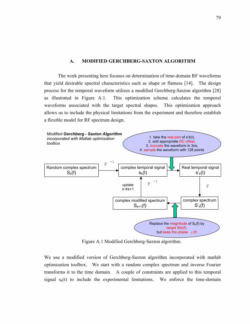
79
A. MODIFIED GERCHBERG-SAXTON ALGORITHM The work presenting here focuses on determination of time-domain RF waveforms
that yield desirable spectral characteristics such as shape or flatness [14]. The design process for the temporal waveform utilizes a modified Gerchberg-Saxton algorithm [28] as illustrated in Figure A.1. This optimization scheme calculates the temporal waveforms associated with the target spectral shapes. This optimization approach allows us to include the physical limitations from the experiment and therefore establish a flexible model for RF spectrum design.
We use a modified version of Gerchberg-Saxton algorithm incorporated with matlab optimization toolbox. We start with a random complex spectrum and inverse Fourier transforms it to the time domain. A couple of constraints are applied to this temporal signal sk(t) to include the experimental limitations. We enforce the time-domain
Modified Gerchberg - Saxton Algorithmincorporated with Matlab optimization toolbox
Replace the magnitude of Sk(f) by target Sth(f),
but keep the phase φ(f)
Random complex spectrum Sk(f)
complex spectrumS’k(f)
complex modified spectrumSk+1(f)
Real temporal signals’k(t)
1. take the real part of s’k(t), 2. add appropriate DC offset,
3. truncate the waveform in 3ns, 4. sample the waveform with 128 points
F -1 Fupdate k k+1
F -1complex temporal signal
sk(t)
Figure A.1 Modified Gerchberg-Saxton algorithm.
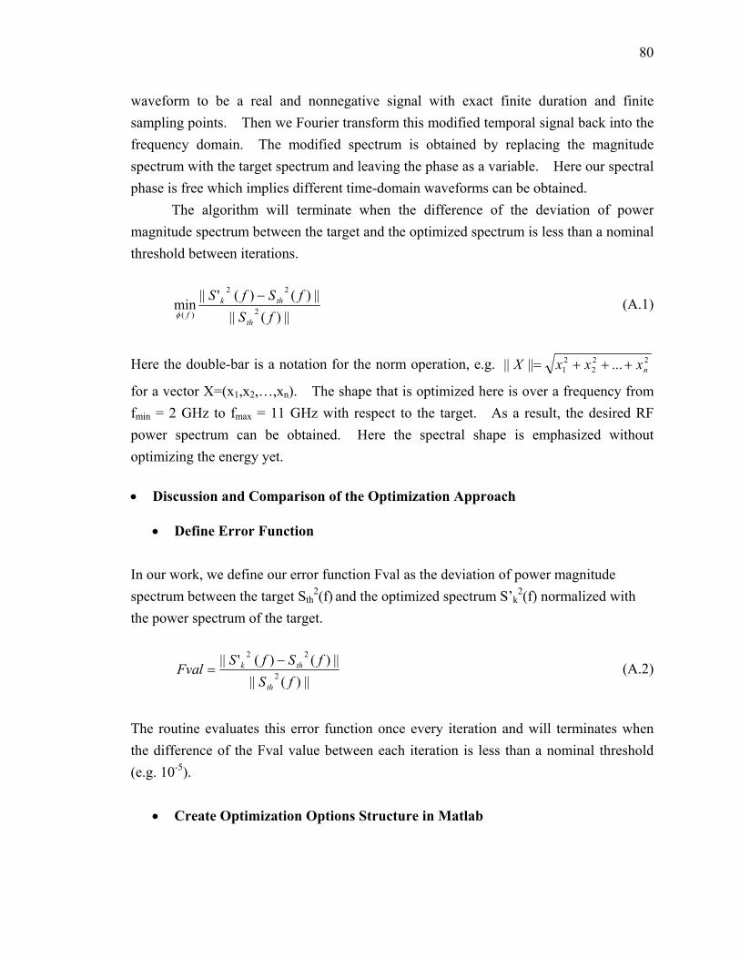
80
waveform to be a real and nonnegative signal with exact finite duration and finite sampling points. Then we Fourier transform this modified temporal signal back into the frequency domain. The modified spectrum is obtained by replacing the magnitude spectrum with the target spectrum and leaving the phase as a variable. Here our spectral phase is free which implies different time-domain waveforms can be obtained.
The algorithm will terminate when the difference of the deviation of power magnitude spectrum between the target and the optimized spectrum is less than a nominal threshold between iterations.
||)(||||)()('||
min 2
22
)( fSfSfS
th
thk
f
−φ
(A.1)
Here the double-bar is a notation for the norm operation, e.g. 22
221 ...|||| nxxxX +++=
for a vector X=(x1,x2,…,xn). The shape that is optimized here is over a frequency from fmin = 2 GHz to fmax = 11 GHz with respect to the target. As a result, the desired RF power spectrum can be obtained. Here the spectral shape is emphasized without optimizing the energy yet. • Discussion and Comparison of the Optimization Approach
• Define Error Function
In our work, we define our error function Fval as the deviation of power magnitude spectrum between the target Sth
2(f) and the optimized spectrum S’k2(f) normalized with
the power spectrum of the target.
||)(||||)()('||
2
22
fSfSfS
Fvalth
thk −=
(A.2)
The routine evaluates this error function once every iteration and will terminates when the difference of the Fval value between each iteration is less than a nominal threshold (e.g. 10-5).
• Create Optimization Options Structure in Matlab
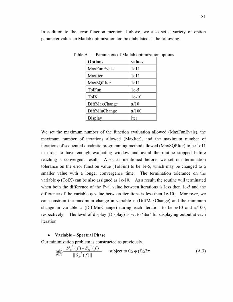
81
In addition to the error function mentioned above, we also set a variety of option parameter values in Matlab optimization toolbox tabulated as the following.
Table A.1 Parameters of Matlab optimization options Options values MaxFunEvals 1e11 MaxIter 1e11 MaxSQPIter 1e11 TolFun 1e-5 TolX 1e-10 DiffMaxChange π/10 DiffMinChange π/100 Display iter
We set the maximum number of the function evaluation allowed (MaxFunEvals), the maximum number of iterations allowed (MaxIter), and the maximum number of iterations of sequential quadratic programming method allowed (MaxSQPIter) to be 1e11 in order to have enough evaluating window and avoid the routine stopped before reaching a convergent result. Also, as mentioned before, we set our termination tolerance on the error function value (TolFun) to be 1e-5, which may be changed to a smaller value with a longer convergence time. The termination tolerance on the variable φ (TolX) can be also assigned as 1e-10. As a result, the routine will terminated when both the difference of the Fval value between iterations is less then 1e-5 and the difference of the variable φ value between iterations is less then 1e-10. Moreover, we can constrain the maximum change in variable φ (DiffMaxChange) and the minimum change in variable φ (DiffMinChange) during each iteration to be π/10 and π/100, respectively. The level of display (Display) is set to ‘iter’ for displaying output at each iteration.
• Variable – Spectral Phase Our minimization problem is constructed as previously,
||)(||
||)()('||min 2
22
)( fSfSfS
th
thk
f
−φ
subject to 0≤ φ (f)≤2π (A.3)
82
where the φ(f) is the spectral phase. In our case, we sampled the spectral phase into 128 phases as a function of frequency {φ(fi), i = 1,2,...128}. The initial values of the variables φ(fi) is 128 random phases limited between 0 and 2π. The Matlab optimization comment we used is called fmincon, which is formatted as
[φ,fval] = fmincon(@myfun,φ0,A,b,Aeq,beq,lb,ub,nonlcon,options) (A.4)
where φ0 is the initial value of the variable. The operation of fmincon is to find a constrained minimum of a scalar function of several variables starting at an initial estimate. The lower bound (lb) is 0 and the upper bound (ub) of the variable is 2π in our case. The input argument ‘@myfun’ is the function to be minimized specified as a function handle for an M-file function. In our case, we plug in our target magnitude spectrum and the procedure of modified Gerchberg-Saxton algorithm (Section 3.2.1) along with the error function Fval into this M-file. The last argument ‘options’ is just the optimization options provided by Matlab mentioned before. We set all the rest input arguments as empty brackets since no constraints of A·x<b, Aeq·x = beq, or nonlinear equations exist in our case. When the routine is completed, the value of the variables φ(fi) and its corresponding evaluated error function value will be returned.
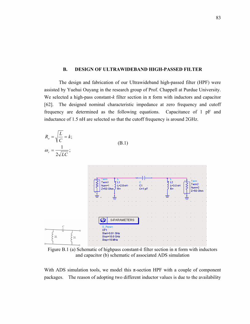
83
B. DESIGN OF ULTRAWIDEBAND HIGH-PASSED FILTER The design and fabrication of our Ultrawideband high-passed filter (HPF) were assisted by Yuehui Ouyang in the research group of Prof. Chappell at Purdue University. We selected a high-pass constant-k filter section in π form with inductors and capacitor [62]. The designed nominal characteristic impedance at zero frequency and cutoff frequency are determined as the following equations. Capacitance of 1 pF and inductance of 1.5 nH are selected so that the cutoff frequency is around 2GHz.
;2
1
;
LC
kCLR
c
o
=
==
ω (B.1)
Figure B.1 (a) Schematic of highpass constant-k filter section in π form with inductors
and capacitor (b) schematic of associated ADS simulation With ADS simulation tools, we model this π-section HPF with a couple of component packages. The reason of adopting two different inductor values is due to the availability
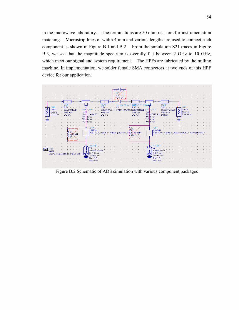
84
in the microwave laboratory. The terminations are 50 ohm resistors for instrumentation matching. Microstrip lines of width 4 mm and various lengths are used to connect each component as shown in Figure B.1 and B.2. From the simulation S21 traces in Figure B.3, we see that the magnitude spectrum is overally flat between 2 GHz to 10 GHz, which meet our signal and system requirement. The HPFs are fabricated by the milling machine. In implementation, we solder female SMA connectors at two ends of this HPF device for our application.
Figure B.2 Schematic of ADS simulation with various component packages
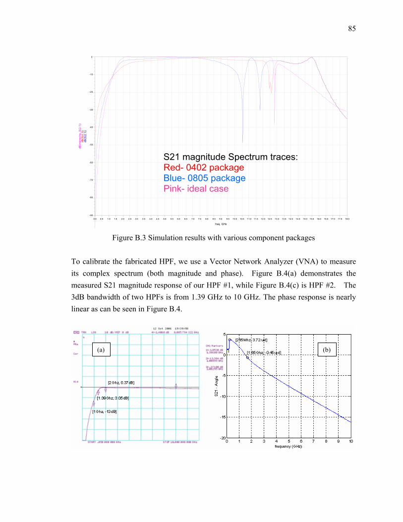
85
Figure B.3 Simulation results with various component packages
To calibrate the fabricated HPF, we use a Vector Network Analyzer (VNA) to measure its complex spectrum (both magnitude and phase). Figure B.4(a) demonstrates the measured S21 magnitude response of our HPF #1, while Figure B.4(c) is HPF #2. The 3dB bandwidth of two HPFs is from 1.39 GHz to 10 GHz. The phase response is nearly linear as can be seen in Figure B.4.
0.5 1.0 1.5 2.0 2.5 3.0 3.5 4.0 4.5 5.0 5.5 6.0 6.5 7.0 7.5 8.0 8.5 9.0 9.5 10.0 10.5 11.0 11.5 12.0 12.5 13.0 13.5 14.0 14.5 15.0 15.5 16.0 16.5 17.0 17.50.0 18.0
-80
-70
-60
-50
-40
-30
-20
-10
-90
0
freq, GHz
dB(S
(2,1
))dB
(S(4
,3))
dB(m
icro
strip
..S(2
,1))
S21 magnitude Spectrum traces: Red- 0402 package Blue- 0805 package Pink- ideal case
(a) (b)
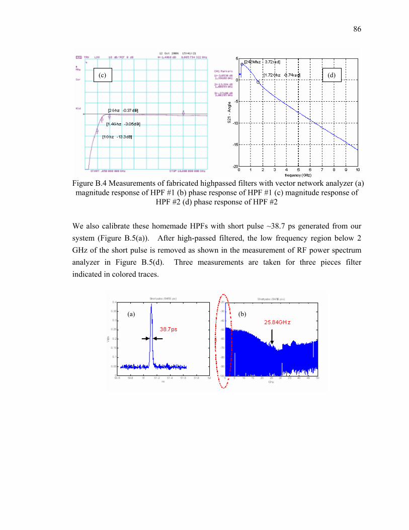
86
Figure B.4 Measurements of fabricated highpassed filters with vector network analyzer (a) magnitude response of HPF #1 (b) phase response of HPF #1 (c) magnitude response of
HPF #2 (d) phase response of HPF #2 We also calibrate these homemade HPFs with short pulse ~38.7 ps generated from our system (Figure B.5(a)). After high-passed filtered, the low frequency region below 2 GHz of the short pulse is removed as shown in the measurement of RF power spectrum analyzer in Figure B.5(d). Three measurements are taken for three pieces filter indicated in colored traces.
(c) (d)
(a) (b)
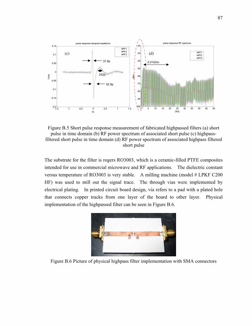
87
Figure B.5 Short pulse response measurement of fabricated highpassed filters (a) short
pulse in time domain (b) RF power spectrum of associated short pulse (c) highpass-filtered short pulse in time domain (d) RF power spectrum of associated highpass filtered
short pulse The substrate for the filter is rogers RO3003, which is a ceramic-filled PTFE composites intended for use in commercial microwave and RF applications. The dielectric constant versus temperature of RO3003 is very stable. A milling machine (model # LPKF C200 HF) was used to mill out the signal trace. The through vias were implemented by electrical plating. In printed circuit board design, via refers to a pad with a plated hole that connects copper tracks from one layer of the board to other layer. Physical implementation of the highpassed filter can be seen in Figure B.6.
Figure B.6 Picture of physical highpass filter implementation with SMA connectors
-1.5 -1 -0.5 0 0.5 1 1.5-0.2
-0.15
-0.1
-0.05
0
0.05
0.1
0.15
ns
Vol
ts
pulse response temporal waveforms
HPF1HPF2HPF3
37.8p
52.9p
242p
0 5 10 15 20 25 30 35 40 45 50-100
-90
-80
-70
-60
-50
-40
-30
-20
GHz
dBm
pulse response RF spectrum
HPF1HPF2HPF3
2.01GHz-
(d)(c)
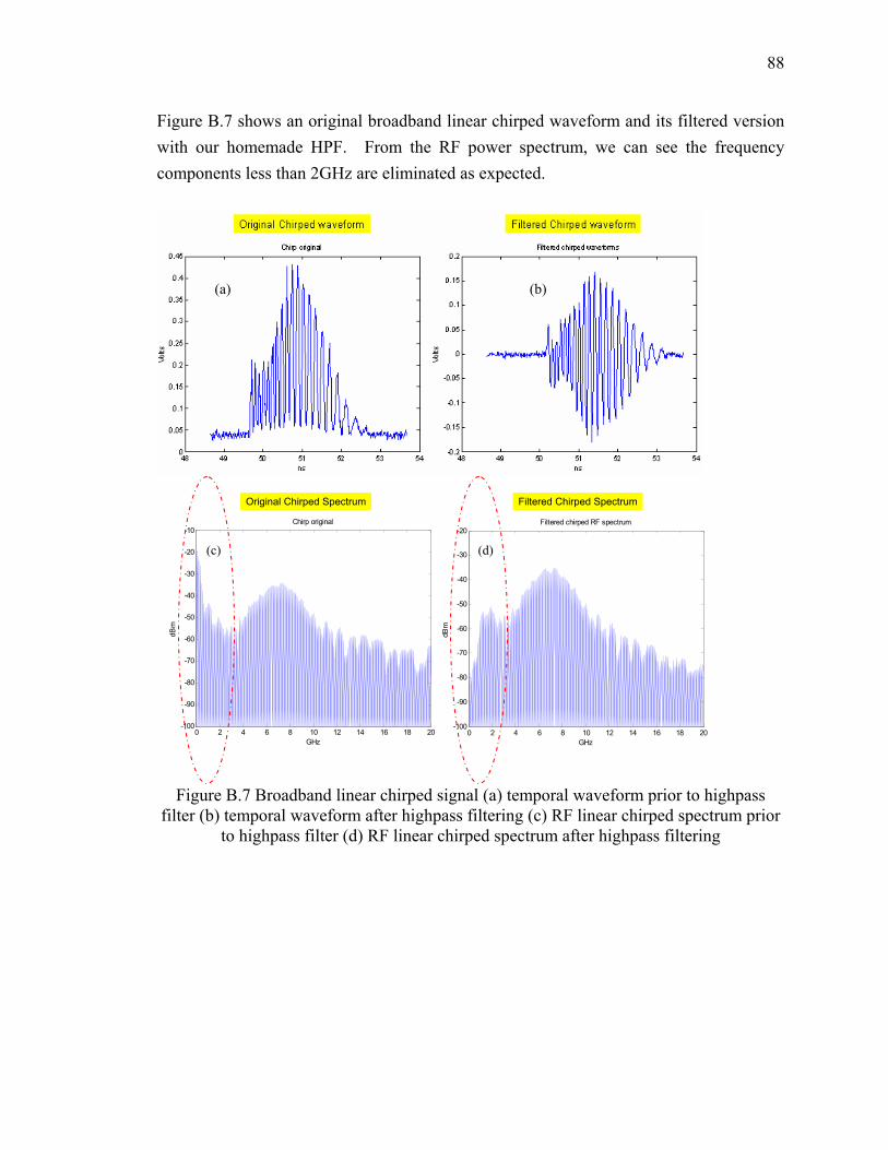
88
Figure B.7 shows an original broadband linear chirped waveform and its filtered version with our homemade HPF. From the RF power spectrum, we can see the frequency components less than 2GHz are eliminated as expected.
Figure B.7 Broadband linear chirped signal (a) temporal waveform prior to highpass
filter (b) temporal waveform after highpass filtering (c) RF linear chirped spectrum prior to highpass filter (d) RF linear chirped spectrum after highpass filtering
0 2 4 6 8 10 12 14 16 18 20-100
-90
-80
-70
-60
-50
-40
-30
-20
GHz
dBm
Filtered chirped RF spectrum
0 2 4 6 8 10 12 14 16 18 20-100
-90
-80
-70
-60
-50
-40
-30
-20
-10
GHz
dBm
Chirp original
Original Chirped Spectrum Filtered Chirped Spectrum
(c) (d)
(a) (b)
89
C. ANALYSIS OF HORN ANTENNA
For modeling a pyramidal horn antenna, the derivation starts from the tangential components of the electrical and magnetic fields and the equivalent current densities over the aperture of the horn antenna, approximated by [58, 63-64]
]2/)/'/'([
1
]2/)/'/'([
1
]2/)/'/'([
1
]2/)/'/'([
1
12
22
12
22
12
22
12
22
)'cos()','(
)'cos()','(
)'cos()','('
)'cos()','('
ρρ
ρρ
ρρ
ρρ
π
πη
πη
π
yxkj
yxkj
yxkj
yxkj
exa
EoyxMx
exa
EoyxJy
exa
EoyxHx
exa
EoyxEy
+−
+−
+−
+−
=
−=
−=
=
(C.1)
The amplitude distribution in the x’ direction is cosinusoidal while the phase variation is quadratic in both x’ and y’ directions. The fields are radiated by sources Js and Ms in the model of aperture antennas, in which the actual radiating sources are replaced by equivalent sources at certain imaginary surface S. And to find the fields radiated by the horn, only the tangential components of the E- and H-fields over a closed surface must be known. The closed surface is chosen to coincide with an infinite plane passing through the mouth of the horn. In the far-zone, only the θ and φ components of the E- and H- field are dominant:
)(4
)(4
0
φθφ
θφθ
ηπ
ηπ
NLr
kejE
NLr
kejE
E
jkr
jkrr
−≅
+−≅
≅
−
−
)(4
)(4
0
ηπ
ηπ
φθφ
θφθ
LN
rkejH
LNr
kejH
H
jkr
jkrr
+−≅
−≅
≅
−
−
21
21
21
21
sincoscos
cos
sincos
IIEoLIIEoL
IIEoN
IIEoN
φφθ
η
φθη
φ
θ
φ
θ
−==
−=
−=
(C.2)
Therefore we can reduce the far-zone E-field as following:
90
])1(cos[cos
4
])cos1([sin4
0
21
21
IIr
kEoejE
IIr
kEoejE
E
jkr
jkrr
+=
+=
=
−
−
θφπ
θφπ
φ
θ
(C.3)
The I1 and I2 are expressed as:
)]})'()'([)]()({[(
)]})''()''([)]''()''({[)]}'()'([)]'()'({[(21
1212)2/'(1
2
1212)2/''(
1212)2/'(2
1
12
22
12
tStSjtCtCek
I
tStSjtCtCetStSjtCtCek
I
kkyj
kkxjkkxj
−−−=
−−−+−−−=
ρ
ρρ
πρ
πρ
where
1
21
22
21
21
cossin'
)'2
(1'
)'2
(1'
akkx
kxkak
t
kxkak
t
πφθ
ρρπ
ρρπ
+=
−=
−−=
1
21
22
21
21
cossin''
)''2
(1''
)''2
(1''
akkx
kxkak
t
kxkak
t
πφθ
ρρπ
ρρπ
−=
−=
−−=
)2
(1
)2
(1
sinsin
11
12
11
11
ρρπ
ρρπ
φθ
kykbk
t
kykbk
t
kky
−=
−−=
=
(C.4)
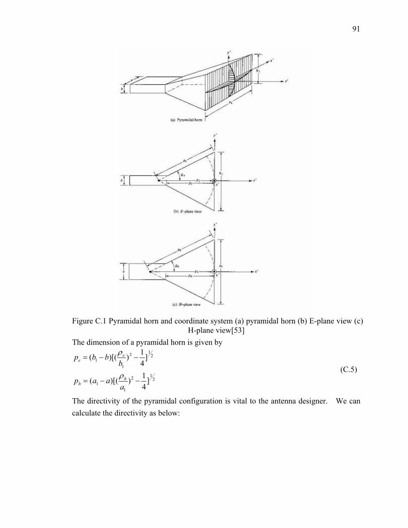
91
Figure C.1 Pyramidal horn and coordinate system (a) pyramidal horn (b) E-plane view (c)
H-plane view[53] The dimension of a pyramidal horn is given by
212
11
212
11
]41))[((
]41))[((
−−=
−−=
aaap
bbbp
hh
ee
ρ
ρ
(C.5)
The directivity of the pyramidal configuration is vital to the antenna designer. We can calculate the directivity as below:
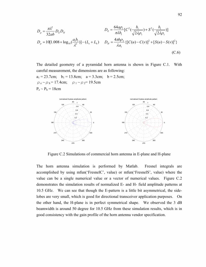
92
)()](log008.1[10
32
211
10
2
hep
HEp
LLbaD
DDab
D
+−+=
=
λ
πλ
})]()([)]()({[4
)]2
()2
([64
22
1
2
1
12
1
12
1
1
vSuSvCuCabD
bSbCb
aD
H
E
−+−=
+=
λρπ
λρλρπλρ
(C.6) The detailed geometry of a pyramidal horn antenna is shown in Figure C.1. With careful measurement, the dimensions are as following: a1 = 23.7cm; b1 = 13.8cm; a = 3.3cm; b = 2.5cm; ρe ~ρh = 17.4cm; ρ1 ~ρ2= 19.5cm Pe ~ Ph = 18cm
0.2
0.4
0.6
0.8
1
30
210
60
240
90
270
120
300
150
330
180 0
normalized E-plane amplitude pattern
0.2
0.4
0.6
0.8
1
30
210
60
240
90
270
120
300
150
330
180 0
normalized H-plane amplitude pattern
Figure C.2 Simulations of commercial horn antenna in E-plane and H-plane
The horn antenna simulation is performed by Matlab. Fresnel integrals are accomplished by using mfun(‘FresnelC’, value) or mfun(‘FresnelS’, value) where the value can be a single numerical value or a vector of numerical values. Figure C.2 demonstrates the simulation results of normalized E- and H- field amplitude patterns at 10.5 GHz. We can see that though the E-pattern is a little bit asymmetrical, the side-lobes are very small, which is good for directional transceiver application purposes. On the other hand, the H-plane is in perfect symmetrical shape. We observed the 3 dB beamwidth is around 50 degree for 10.5 GHz from these simulation results, which is in good consistency with the gain profile of the horn antenna vendor specification.
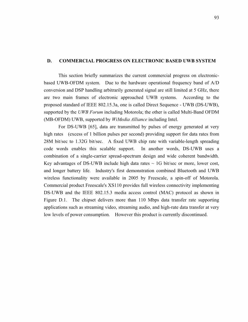
93
D. COMMERCIAL PROGRESS ON ELECTRONIC BASED UWB SYSTEM
This section briefly summarizes the current commercial progress on electronic-based UWB-OFDM system. Due to the hardware operational frequency band of A/D conversion and DSP handling arbitrarily generated signal are still limited at 5 GHz, there are two main frames of electronic approached UWB systems. According to the proposed standard of IEEE 802.15.3a, one is called Direct Sequence - UWB (DS-UWB), supported by the UWB Forum including Motorola; the other is called Multi-Band OFDM (MB-OFDM) UWB, supported by WiMedia Alliance including Intel. For DS-UWB [65], data are transmitted by pulses of energy generated at very high rates (excess of 1 billion pulses per second) providing support for data rates from 28M bit/sec to 1.32G bit/sec. A fixed UWB chip rate with variable-length spreading code words enables this scalable support. In another words, DS-UWB uses a combination of a single-carrier spread-spectrum design and wide coherent bandwidth. Key advantages of DS-UWB include high data rates ~ 1G bit/sec or more, lower cost, and longer battery life. Industry's first demonstration combined Bluetooth and UWB wireless functionality were available in 2005 by Freescale, a spin-off of Motorola. Commercial product Freescale's XS110 provides full wireless connectivity implementing DS-UWB and the IEEE 802.15.3 media access control (MAC) protocol as shown in Figure D.1. The chipset delivers more than 110 Mbps data transfer rate supporting applications such as streaming video, streaming audio, and high-rate data transfer at very low levels of power consumption. However this product is currently discontinued.
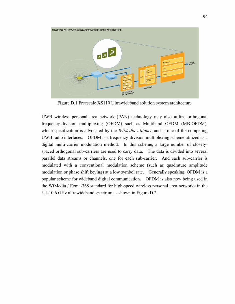
94
Figure D.1 Freescale XS110 Ultrawideband solution system architecture
UWB wireless personal area network (PAN) technology may also utilize orthogonal frequency-division multiplexing (OFDM) such as Multiband OFDM (MB-OFDM), which specification is advocated by the WiMedia Alliance and is one of the competing UWB radio interfaces. OFDM is a frequency-division multiplexing scheme utilized as a digital multi-carrier modulation method. In this scheme, a large number of closely-spaced orthogonal sub-carriers are used to carry data. The data is divided into several parallel data streams or channels, one for each sub-carrier. And each sub-carrier is modulated with a conventional modulation scheme (such as quadrature amplitude modulation or phase shift keying) at a low symbol rate. Generally speaking, OFDM is a popular scheme for wideband digital communication. OFDM is also now being used in the WiMedia / Ecma-368 standard for high-speed wireless personal area networks in the 3.1-10.6 GHz ultrawideband spectrum as shown in Figure D.2.
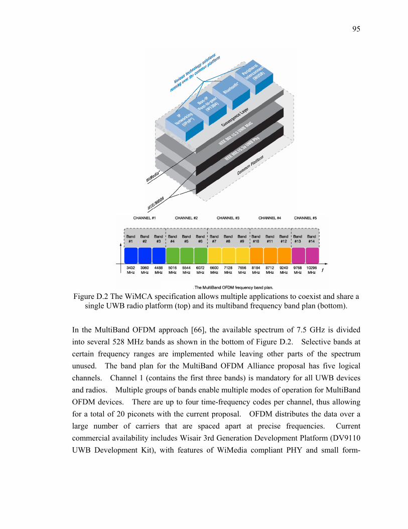
95
Figure D.2 The WiMCA specification allows multiple applications to coexist and share a
single UWB radio platform (top) and its multiband frequency band plan (bottom). In the MultiBand OFDM approach [66], the available spectrum of 7.5 GHz is divided into several 528 MHz bands as shown in the bottom of Figure D.2. Selective bands at certain frequency ranges are implemented while leaving other parts of the spectrum unused. The band plan for the MultiBand OFDM Alliance proposal has five logical channels. Channel 1 (contains the first three bands) is mandatory for all UWB devices and radios. Multiple groups of bands enable multiple modes of operation for MultiBand OFDM devices. There are up to four time-frequency codes per channel, thus allowing for a total of 20 piconets with the current proposal. OFDM distributes the data over a large number of carriers that are spaced apart at precise frequencies. Current commercial availability includes Wisair 3rd Generation Development Platform (DV9110 UWB Development Kit), with features of WiMedia compliant PHY and small form-
96
factor of 4 x 6cm. It is designed for data rates up to 480 Mbps and frequency range of 3.1 to 4.8 GHz, supporting three 528 MHz sub-bands under MB-OFDM modulation [67]. Abundant industrial interests imply UWB system is one of the prominent wireless communication schemes. Comparing to the abovementioned electronic approach products, our photonically-assisted UWB communication system can handle larger instantaneous bandwidth with a real-time detection capability.

VITA
97
VITA
Ingrid S. Lin received the B.S. degree (with highest honors) in Communication Engineering from National Chiao-Tung University, Hsinchu, Taiwan in 2002, and is currently working toward the Ph.D. degree at Purdue University, West Lafayette, IN. She received a Graduate Fellowship (supported by General Electric) from Purdue University, where she is currently a Research Assistant with the School of Electrical and Computer Engineering. Her current research interest is in ultrafast optics focusing on optical pulse shaping, arbitrary waveform generation, and RF photonics with applications in Ultra-wide bandwidth communication. She has authored or coauthored 3 journal papers and 12 conference papers. Ms. Lin is a member of the IEEE Lasers and Electro-Optics Society. She was listed in the National Science Foundation (NSF) Graduate Fellowship Honorable Mentions in 2003. She was also a recipient of the Graduate Assistance in Areas of National Need (GAANN) Fellowship (2003–2006).


![Silicon-Based Integrated Microwave Photonicsjpyao/mprg/reprints/JQE_SiP-MWP-final.pdf · Among the applications, photonic generation of arbitrary microwave waveforms [7] and photonic](https://img.pdfslide.us/doc/110x75/5edc4175ad6a402d6666d914/silicon-based-integrated-microwave-jpyaomprgreprintsjqesip-mwp-finalpdf-among.jpg)