Embed Size (px)
Citation preview
1
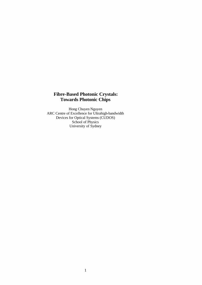
Fibre-Based Photonic Crystals:
Towards Photonic Chips
Hong Chuyen Nguyen ARC Centre of Excellence for Ultrahigh-bandwidth
Devices for Optical Systems (CUDOS) School of Physics
University of Sydney
Abstract
Photonic crystals are a sought-after materia l for photonic chip applications. Existing fabrication methods are not entirely suitable for such an application either because they are time consuming, expensive, and/or lack the ability to insert controlled defects. In this thesis we introduce microstructured optical fibres (MOFs) in a completely new context, as a novel photonic crystal geometry. For the first time, we use MOFs not as a “light-pipe”, but in the transverse geometry to manipulate the light propagating across the fibre. This concept was motivated by its simple and mature fabrication methods and the possibility of arbitrary hole structures, as well as its ability to be tuned with microfluidics. Fundamental and higher-order partial bandgaps were observed along the symmetry axes of the fibre microstructure, using Fourier Transform Infrared spectroscopy in the 1.4 - 4 µm wavelength range and an optical spectrum analyzer in the 0.8 – 1.7 µm range. Measured spectra were compared with band structure and Finite-Difference Time Domain simulations, and showed compelling evidence that the spectral features are indeed a result of the periodic nature of the microstructure. A simple but tuneable device application was also demonstrated, by the displacement of fluids into the holes of the fibre and observing the change in spectra.
3
Acknowledgements
I would first like to thank my supervisor, Ben Eggleton, and co-supervisor, Maryanne Large, for their constant and often overwhelming enthusiasm and support for this project. They have both contributed significantly to the knowledge and skills that I have acquired, both in and outside the lab. There are many people who needs to be thanked for their contribution to the experimental component of this thesis. I would like to thank Jeremy Bolger for his advice and help in the familiarization with generic skills required in an optics lab; Peter Domachuk for his conceptual contribution in setting up the imaging system used to observe the fibre orientation, and also for the development of the fluid-insertion method which I used to demonstrate the tuneable device concept; Martin Straub and Min Gu at the Centre for Micro-Photonics, Swinburne University of Technology, for their assistance in the FTIR spectroscopy during my visit; Vahid Ta’eed and Ian Kaplin for their assistance in the scanning electron microscopy of the fibre; and Whayne Padden and Barry Reed at the Optical Fibre Technology Centre for the fabrication of the “superprism” fibre (shown in Chapter 7), the specification of which I submitted. A special thanks to Mike Steel for his assistance in learning, and the initial setting up of the simulation geometry in, FullWAVE™ FDTD simulation package. Also thanks to Mike and Paul Steinvurzel for their initial contributions in the familiarization with the BandSOLVE™ software. I would also like to thank Martijn de Sterke, Ross McPhedran, David Fussell and Nicolae Nicorovici for their contribution to my understanding of the background theories, in particular with band structures. I would also like to thank Dick Collins and Susan Eggleton for the editing of sections of this thesis; Ross McKerracher for his occasional assistance with Matlab commands; and Sydney Vislab for the software tools used to generate animation as part of this project. This year would certainly have not been as enjoyable as it has, without the great company of the Physics Honours class. In particular, my office-mates Jackie, Sam, and Trina have been a great source of entertainment, ridicule, embarrassment, knowledge and sugar, all of which were invaluable. Also thanks to Al, Fitz, Jock, Kat and Shelley for being great class mates. I must also thank my family – Mum, Dad and Hong Dao – for their unlimited support throughout the year. In particular, I thank Mum for the constant supply of nutrition that would keep me going from the wee hours of morning to the wee hours of the evening. Thanks must also go to my cousin Teruaki for his support, and also to his family and pet dog Chiruta for food and general entertainment. I would also like to thank Fiona Phan, Vu Lam and their families, for without their generous and mind-calming hospitality, my visit to Melbourne for the FTIR measurements would otherwise have been extremely stressful. Further, I would like to thank the students, staff and volunteers from the 2003 Professor Harry Messel International Science School, and members of the Young Scientists of Australia, Sydney Chapter; St. John Ambulance, Sydney Uni Division; and the Sydney Uni Judo Club, for being my contacts to the outside world. Their activities have certainly been pleasant (and occasionally painful) and necessary distractions from work. On that note, thanks also to Anna Hi, Candy Fung, Flora Chiu and Hai Ho for being great friends and offering their time over lunch breaks. Also thanks to the many 1st Year students I have met and the “disciples” I have acquired, especially to those who contributed to Hong’s Hunger-Management Fund. Finally, a very special thanks to Nicole Mealing and Bridget Honan for being invaluable friends and holding me together emotionally on many occasions. Their support and friendship have certainly reduced the amount of unnecessary blood, sweat and tears that has flowed this year.
I certify that this Thesis contains work carried out by myself except where otherwise acknowledged.
Signed _________________
October 26, 2003
4
Contents
1 Introduction........................................................................................................................... 1
1.1 The Need for Photonic Chips ..............................................................................................5 1.2 Photonic Crystals ...............................................................................................................5 1.3 Microstructured Optical Fibres............................................................................................5 1.4 Thesis Aim and Motivation.................................................................................................5
2 Survey of the Field.................................................................................................................. 7
2.1 History – From the Study of 1D Photonic Crystals ...............................................................7 2.2 Solid State Physics and the Generalisation to Higher Dimensions ..........................................8 2.3 The Impact of Photonic Crystals .........................................................................................9
2.3.1 Photonic Chip Concepts – Controlling the Flow of Light.............................................9 2.4 Fabrication of PCs and MOFs ...........................................................................................11
2.4.1 The Challenge ........................................................................................................11 2.4.2 Naturally Occurring Photonic Crystals .....................................................................12 2.4.3 Current Fabrication Methods ...................................................................................12
3 Fibre Structure & Background Theory ................................................................................ 15
3.1 Fibre Geometry................................................................................................................15 3.1.1 Light Propagation Through the Fibre .......................................................................16
3.2 Theoretical Background....................................................................................................16 3.2.1 2D Approximation ..................................................................................................16 3.2.2 Band Structure........................................................................................................17 3.2.3 Finite-Difference Time Domain ...............................................................................18
4 Fundamental Bandgap ......................................................................................................... 20
4.1 Experimental Method .......................................................................................................20 4.1.1 Instrument..............................................................................................................20 4.1.2 Specimen Preparation .............................................................................................20 4.1.3 Measurement Procedure..........................................................................................20
4.2 Results and Analysis ........................................................................................................21
5 Higher-Order Bandgap ........................................................................................................ 24
5.1 Experimental Method .......................................................................................................24 5.1.1 Fibre Orientation and Alignment .............................................................................24 5.1.2 Polarisation ............................................................................................................25 5.1.3 Measurements ........................................................................................................26
5.2 Experimental Results & Band Structure.............................................................................26 5.3 Experimental Results and FDTD Simulation ......................................................................27 5.4 Analysis of Calculated Spectra..........................................................................................28 5.5 Discussion .......................................................................................................................30
6 Tuneable Device Concept ..................................................................................................... 32
6.1 Fluid Insertion .................................................................................................................32 6.2 Effect on the Fundamental Bandgap ..................................................................................32 6.3 Effect on the Higher-Order Bandgap .................................................................................34
7 Conclusion and Further Work ............................................................................................. 36
5
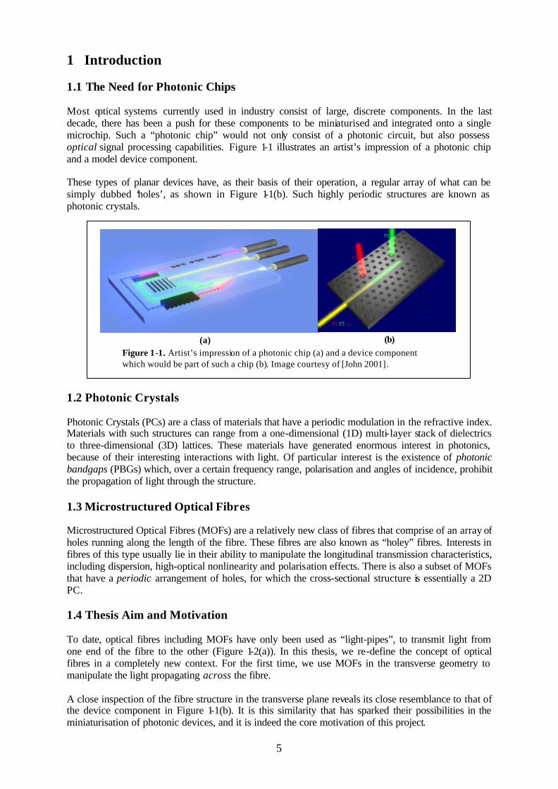
1 Introduction 1.1 The Need for Photonic Chips Most optical systems currently used in industry consist of large, discrete components. In the last decade, there has been a push for these components to be miniaturised and integrated onto a single microchip. Such a “photonic chip” would not only consist of a photonic circuit, but also possess optical signal processing capabilities. Figure 1-1 illustrates an artist’s impression of a photonic chip and a model device component. These types of planar devices have, as their basis of their operation, a regular array of what can be simply dubbed ‘holes’, as shown in Figure 1-1(b). Such highly periodic structures are known as photonic crystals.
1.2 Photonic Crystals Photonic Crystals (PCs) are a class of materials that have a periodic modulation in the refractive index. Materials with such structures can range from a one-dimensional (1D) multi-layer stack of dielectrics to three-dimensional (3D) lattices. These materials have generated enormous interest in photonics, because of their interesting interactions with light. Of particular interest is the existence of photonic bandgaps (PBGs) which, over a certain frequency range, polarisation and angles of incidence, prohibit the propagation of light through the structure. 1.3 Microstructured Optical Fibres Microstructured Optical Fibres (MOFs) are a relatively new class of fibres that comprise of an array of holes running along the length of the fibre. These fibres are also known as “holey” fibres. Interests in fibres of this type usually lie in their ability to manipulate the longitudinal transmission characteristics, including dispersion, high-optical nonlinearity and polarisation effects. There is also a subset of MOFs that have a periodic arrangement of holes, for which the cross-sectional structure is essentially a 2D PC. 1.4 Thesis Aim and Motivation To date, optical fibres including MOFs have only been used as “light-pipes”, to transmit light from one end of the fibre to the other (Figure 1-2(a)). In this thesis, we re-define the concept of optical fibres in a completely new context. For the first time, we use MOFs in the transverse geometry to manipulate the light propagating across the fibre. A close inspection of the fibre structure in the transverse plane reveals its close resemblance to that of the device component in Figure 1-1(b). It is this similarity that has sparked their possibilities in the miniaturisation of photonic devices, and it is indeed the core motivation of this project.
(a) (b) Figure 1-1. Artist’s impression of a photonic chip (a) and a device component which would be part of such a chip (b). Image courtesy of [John 2001].
6
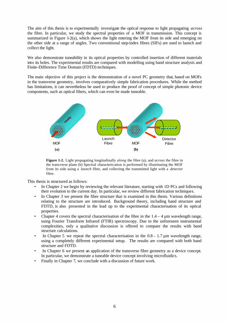
The aim of this thesis is to experimentally investigate the optical response to light propagating across the fibre. In particular, we study the spectral properties of a MOF in transmission. This concept is summarized in Figure 1-2(a), which shows the light entering the MOF from its side and emerging on the other side at a range of angles. Two conventional step-index fibres (SIFs) are used to launch and collect the light. We also demonstrate tuneability in its optical properties by controlled insertion of different materials into its holes. The experimental results are compared with modelling using band structure analysis and Finite-Difference Time Domain (FDTD) techniques. The main objective of this project is the demonstration of a novel PC geometry that, based on MOFs in the transverse geometry, involves comparatively simple fabrication procedures. While the method has limitations, it can nevertheless be used to produce the proof of concept of simple photonic device components, such as optical filters, which can even be made tuneable.
This thesis is structured as follows: • In Chapter 2 we begin by reviewing the relevant literature, starting with 1D PCs and following
their evolution to the current day. In particular, we review different fabrication techniques. • In Chapter 3 we present the fibre structure that is examined in this thesis. Various definitions
relating to the structure are introduced. Background theory, including band structure and FDTD, is also presented in the lead up to the experimental characterisation of its optical properties.
• Chapter 4 covers the spectral characterisation of the fibre in the 1.4 – 4 µm wavelength range, using Fourier Transform Infrared (FTIR) spectroscopy. Due to the unforeseen instrumental complexities, only a qualitative discussion is offered to compare the results with band structure calculations.
• In Chapter 5 we repeat the spectral characterisation in the 0.8 – 1.7 µm wavelength range, using a completely different experimental setup. The results are compared with both band structure and FDTD.
• In Chapter 6 we present an application of the transverse fibre geometry as a device concept. In particular, we demonstrate a tuneable device concept involving microfluidics.
• Finally in Chapter 7, we conclude with a discussion of future work.
Launch Fibre
Figure 1-2. Light propagating longitudinally along the fibre (a), and across the fibre in the transverse plane (b) Spectral characteris ation is performed by illuminating the MOF from its side using a launch fibre, and collecting the transmitted light with a detector fibre.
MOF
(b)
MOF
(a)
Detector Fibre
7
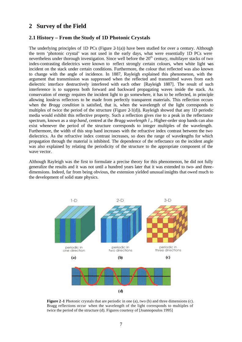
2 Survey of the Field 2.1 History – From the Study of 1D Photonic Crystals The underlying principles of 1D PCs (Figure 2-1(a)) have been studied for over a century. Although the term ‘photonic crystal’ was not used in the early days, what were essentially 1D PCs were nevertheless under thorough investigation. Since well before the 20th century, multilayer stacks of two index-contrasting dielectrics were known to reflect strongly certain colours, when white light was incident on the stack under certain conditions. Furthermore, the colour that reflected was also known to change with the angle of incidence. In 1887, Rayleigh explained this phenomenon, with the argument that transmission was suppressed when the reflected and transmitted waves from each dielectric interface destructively interfered with each other [Rayleigh 1887]. The result of such interference is to suppress both forward and backward propagating waves inside the stack. As conservation of energy requires the incident light to go somewhere, it has to be reflected, in principle allowing lossless reflectors to be made from perfectly transparent materials. This reflection occurs when the Bragg condition is satisfied, that is, when the wavelength of the light corresponds to multiples of twice the period of the structure (Figure 2-1(d)). Rayleigh showed that any 1D periodic media would exhibit this reflective property. Such a reflection gives rise to a peak in the reflectance spectrum, known as a stop band, centred at the Bragg wavelength λ0. Higher-order stop bands can also exist whenever the period of the structure corresponds to integer multiples of the wavelength. Furthermore, the width of this stop band increases with the refractive index contrast between the two dielectrics. As the refractive index contrast increases, so does the range of wavelengths for which propagation through the material is inhibited. The dependence of the reflectance on the incident angle was also explained by relating the periodicity of the structure to the appropriate component of the wave vector. Although Rayleigh was the first to formulate a precise theory for this phenomenon, he did not fully generalize the results and it was not until a hundred years later that it was extended to two- and three-dimensions. Indeed, far from being obvious, the extension yielded unusual insights that owed much to the development of solid state physics.
(a)
(b)
(c)
(d)
Figure 2 -1 Photonic crystals that are periodic in one (a), two (b) and three dimensions (c). Bragg reflections occur when the wavelength of the light corresponds to multiples of twice the period of the structure (d). Figures courtesy of [Joannopoulos 1995]
8
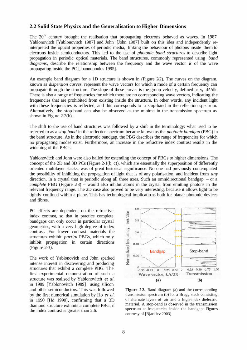
2.2 Solid State Physics and the Generalisation to Higher Dimensions The 20th century brought the realisation that propagating electrons behaved as waves. In 1987 Yablonovitch [Yablonovitch 1987] and John [John 1987] built on this idea and independently re-interpreted the optical properties of periodic media, linking the behaviour of photons inside them to electrons inside semiconductors. This led to the use of photonic band structures to describe light propagation in periodic optical materials. The band structures, commonly represented using band diagrams, describe the relationship between the frequency and the wave vector k of the wave propagating inside the PC [Joannopoulos 1995]. An example band diagram for a 1D structure is shown in (Figure 2-2). The curves on the diagram, known as dispersion curves, represent the wave vectors for which a mode of a certain frequency can propagate through the structure. The slope of these curves is the group velocity, defined as vg=d? /dk. There is also a range of frequencies for which there are no corresponding wave vectors, indicating the frequencies that are prohibited from existing inside the structure. In other words, any incident light with these frequencies is reflected, and this corresponds to a stop-band in the reflection spectrum. Alternatively, the stop-band can also be observed as the minima in the transmission spectrum as shown in Figure 2-2(b). The shift to the use of band structures was followed by a shift in the terminology: what used to be referred to as a stop-band in the reflection spectrum became known as the photonic bandgap (PBG) in the band structure. As in the electronic bandgap, the PBG describes the range of frequencies for which no propagating modes exist. Furthermore, an increase in the refractive index contrast results in the widening of the PBGs. Yablonovitch and John were also hailed for extending the concept of PBGs to higher dimensions. The concept of the 2D and 3D PCs (Figure 2-1(b, c)), which are essentially the superposition of differently oriented multilayer stacks, was of great historical significance. No one had previously contemplated the possibility of inhibiting the propagation of light that is of any polarisation, and incident from any direction, in a crystal that is periodic along all three axes. Such an omnidirectional bandgap – or a complete PBG (Figure 2-3) – would also inhibit atoms in the crystal from emitting photons in the relevant frequency range. The 2D case also proved to be very interesting, because it allows light to be tightly confined within a plane. This has technological implications both for planar photonic devices and fibres. PC effects are dependent on the refractive index contrast, so that in practice complete bandgaps can only occur in particular crystal geometries, with a very high degree of index contrast. For lower contrast materials the structures exhibit partial PBGs, which only inhibit propagation in certain directions (Figure 2-3). The work of Yablonovich and John sparked intense interest in discovering and producing structures that exhibit a complete PBG. The first experimental demonstration of such a structure was realised by Yablonovitch et al. in 1989 [Yablonovitch 1989] , using silicon and other semiconductors. This was followed by the first numerical simulation by Ho et al. in 1990 [Ho 1990], confirming that a 3D diamond structure exhibits a complete PBG, if the index contrast is greater than 2.6.
Bandgap
(b)
(a)
Figure 2-2. Band diagram (a) and the corresponding transmission spectrum (b) for a Bragg stack consisting of alternate layers of air and a high-index dielectric material. A stop-band is observed in the transmission spectrum at frequencies inside the bandgap. Figures courtesy of [Bjarklev 2003]
Stop-band
9
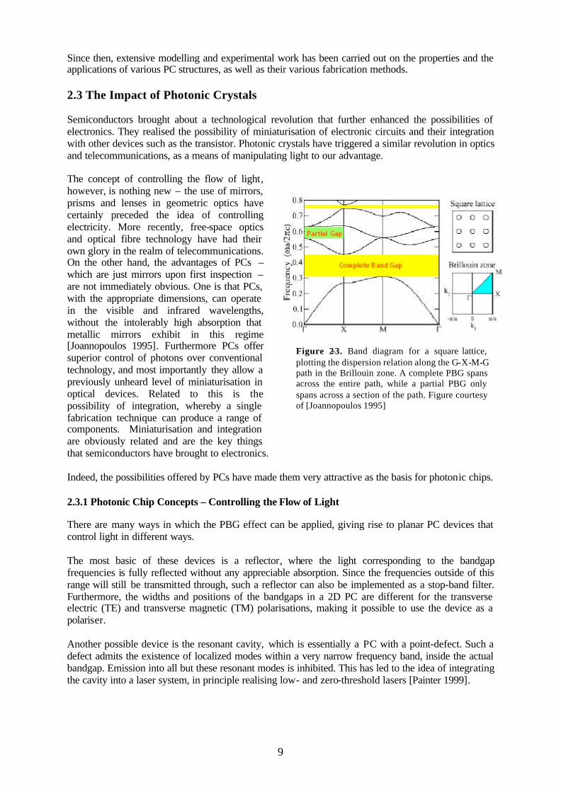
Figure 2-3. Band diagram for a square lattice, plotting the dispersion relation along the G-X-M-G path in the Brillouin zone. A complete PBG spans across the entire path, while a partial PBG only spans across a section of the path. Figure courtesy of [Joannopoulos 1995]
Since then, extensive modelling and experimental work has been carried out on the properties and the applications of various PC structures, as well as their various fabrication methods. 2.3 The Impact of Photonic Crystals Semiconductors brought about a technological revolution that further enhanced the possibilities of electronics. They realised the possibility of miniaturisation of electronic circuits and their integration with other devices such as the transistor. Photonic crystals have triggered a similar revolution in optics and telecommunications, as a means of manipulating light to our advantage. The concept of controlling the flow of light, however, is nothing new – the use of mirrors, prisms and lenses in geometric optics have certainly preceded the idea of controlling electricity. More recently, free-space optics and optical fibre technology have had their own glory in the realm of telecommunications. On the other hand, the advantages of PCs – which are just mirrors upon first inspection – are not immediately obvious. One is that PCs, with the appropriate dimensions, can operate in the visible and infrared wavelengths, without the intolerably high absorption that metallic mirrors exhibit in this regime [Joannopoulos 1995]. Furthermore PCs offer superior control of photons over conventional technology, and most importantly they allow a previously unheard level of miniaturisation in optical devices. Related to this is the possibility of integration, whereby a single fabrication technique can produce a range of components. Miniaturisation and integration are obviously related and are the key things that semiconductors have brought to electronics. Indeed, the possibilities offered by PCs have made them very attractive as the basis for photonic chips. 2.3.1 Photonic Chip Concepts – Controlling the Flow of Light There are many ways in which the PBG effect can be applied, giving rise to planar PC devices that control light in different ways. The most basic of these devices is a reflector, where the light corresponding to the bandgap frequencies is fully reflected without any appreciable absorption. Since the frequencies outside of this range will still be transmitted through, such a reflector can also be implemented as a stop-band filter. Furthermore, the widths and positions of the bandgaps in a 2D PC are different for the transverse electric (TE) and transverse magnetic (TM) polarisations, making it possible to use the device as a polariser. Another possible device is the resonant cavity, which is essentially a PC with a point-defect. Such a defect admits the existence of localized modes within a very narrow frequency band, inside the actual bandgap. Emission into all but these resonant modes is inhibited. This has led to the idea of integrating the cavity into a laser system, in principle realising low- and zero-threshold lasers [Painter 1999].
10
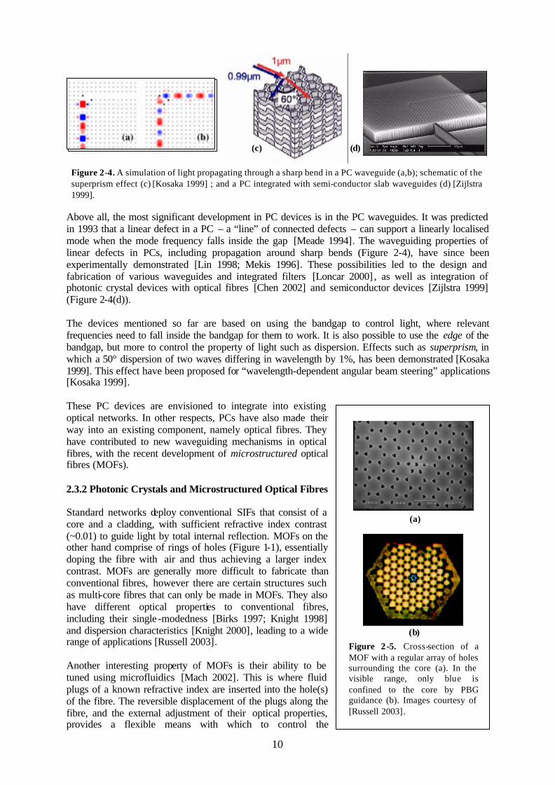
Above all, the most significant development in PC devices is in the PC waveguides. It was predicted in 1993 that a linear defect in a PC – a “line” of connected defects – can support a linearly localised mode when the mode frequency falls inside the gap [Meade 1994]. The waveguiding properties of linear defects in PCs, including propagation around sharp bends (Figure 2-4), have since been experimentally demonstrated [Lin 1998; Mekis 1996]. These possibilities led to the design and fabrication of various waveguides and integrated filters [Loncar 2000] , as well as integration of photonic crystal devices with optical fibres [Chen 2002] and semiconductor devices [Zijlstra 1999] (Figure 2-4(d)). The devices mentioned so far are based on using the bandgap to control light, where relevant frequencies need to fall inside the bandgap for them to work. It is also possible to use the edge of the bandgap, but more to control the property of light such as dispersion. Effects such as superprism, in which a 50° dispersion of two waves differing in wavelength by 1%, has been demonstrated [Kosaka 1999]. This effect have been proposed for “wavelength-dependent angular beam steering” applications [Kosaka 1999]. These PC devices are envisioned to integrate into existing optical networks. In other respects, PCs have also made their way into an existing component, namely optical fibres. They have contributed to new waveguiding mechanisms in optical fibres, with the recent development of microstructured optical fibres (MOFs). 2.3.2 Photonic Crystals and Microstructured Optical Fibres Standard networks deploy conventional SIFs that consist of a core and a cladding, with sufficient refractive index contrast (~0.01) to guide light by total internal reflection. MOFs on the other hand comprise of rings of holes (Figure 1-1), essentially doping the fibre with air and thus achieving a larger index contrast. MOFs are generally more difficult to fabricate than conventional fibres, however there are certain structures such as multi-core fibres that can only be made in MOFs. They also have different optical properties to conventional fibres, including their single -modedness [Birks 1997; Knight 1998] and dispersion characteristics [Knight 2000], leading to a wide range of applications [Russell 2003]. Another interesting property of MOFs is their ability to be tuned using microfluidics [Mach 2002]. This is where fluid plugs of a known refractive index are inserted into the hole(s) of the fibre. The reversible displacement of the plugs along the fibre, and the external adjustment of their optical properties, provides a flexible means with which to control the
(c)
Figure 2-4. A simulation of light propagating through a sharp bend in a PC waveguide (a,b); schematic of the superprism effect (c) [Kosaka 1999] ; and a PC integrated with semi-conductor slab waveguides (d) [Zijlstra 1999].
(d)
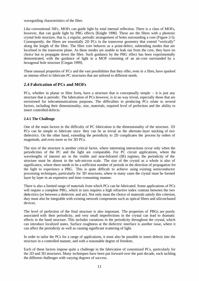
Figure 2 -5. Cross-section of a MOF with a regular array of holes surrounding the core (a). In the visible range, only blue is confined to the core by PBG guidance (b). Images courtesy of [Russell 2003].
(a)
(b)
11
waveguiding characteristics of the fibre. Like conventional SIFs , MOFs can guide light by total internal reflection. There is a class of MOFs, however, that can guide light by PBG effects [Knight 1998]. These are the fibres with a photonic crystal hole structure, that is, a regular, periodic arrangement of holes surrounding a core (Figure 2-5). Consequently, the fibres are essentially 2D PCs in the transverse geometry that extend “vertically” along the length of the fibre. The fibre core behaves as a point-defect, subtending modes that are localised in the transverse plane. As these modes are unable to leak out from the core, they have no choice but to propagate down the fibre. Such guidance by the PBG effect has been experimentally demonstrated, with the guidance of light in a MOF consisting of an air-core surrounded by a hexagonal hole structure [Cregan 1999]. These unusual properties of PCs and the vast possibilities that they offer, even in a fibre, have sparked an intense effort to fabricate PC structures that are tailored to different needs. 2.4 Fabrication of PCs and MOFs PCs, whether in planar or fibre form, have a structure that is conceptually simple – it is just any structure that is periodic. The fabrication of PCs however, is in no way trivial, especially those that are envisioned for telecommunications purposes. The difficulties in producing PCs relate to several factors, including their dimensionality, size, materials, required level of perfection and the ability to insert controlled defects. 2.4.1 The Challenge One of the main factors in the difficulty of PC fabrication is the dimensionality of the structure. 1D PCs can be simple to fabricate since they can be as trivial as the alternate-layer stacking of two dielectrics. On the other hand, extending the periodicity to 2D complicates the process by orders of magnitude, and even more so for 3D PCs. The size of the structure is another critical factor, where interesting interactions occur only when the periodicities of the PC and the light are comparable. For PC circuit applications, where the wavelengths of interest are in the visible and near-Infrared (IR) regimes, the periodicity of the structure must be almost in the sub-micron scale. The size of the crystal as a whole is also of significance, where there needs to be a sufficient number of periods in the direction of propagation for the light to experience a PBG. This is quite difficult to achieve using existing semiconductor processing techniques, particularly for 3D structures, where in many cases the crystal must be formed layer by layer in an expensive and time-consuming manner. There is also a limited range of materials from which PCs can be fabricated. Some applications of PCs will require a complete PBG, which in turn requires a high refractive index contrast between the two dielectrics (or between a dielectric and air). Not only must the choice of materials satisfy this criterion, they must also be integrable with existing network components such as optical fibres and silicon-based devices. The level of perfection of the final structure is also important. The properties of PBGs are purely associated with their periodicity, and very small imperfections in the crystal can lead to dramatic effects in the band structure. This includes variations in the periodicity throughout the crystal, which can introduce localized states. Surface roughness at the dielectric interface is another issue, where it can affect the periodicity as well as causing significant scattering of light. In order to tailor the PCs for a range of applications, it must also be possible to insert defects into the structure in a controlled manner, and with a reasonable degree of freedom. Each of these factors impose quite a challenge in the fabrication of customized PCs, particularly for the 2D and 3D structures. Many techniques have been put forward over the past decade, each tackling the different challenges with varying degrees of success.
12
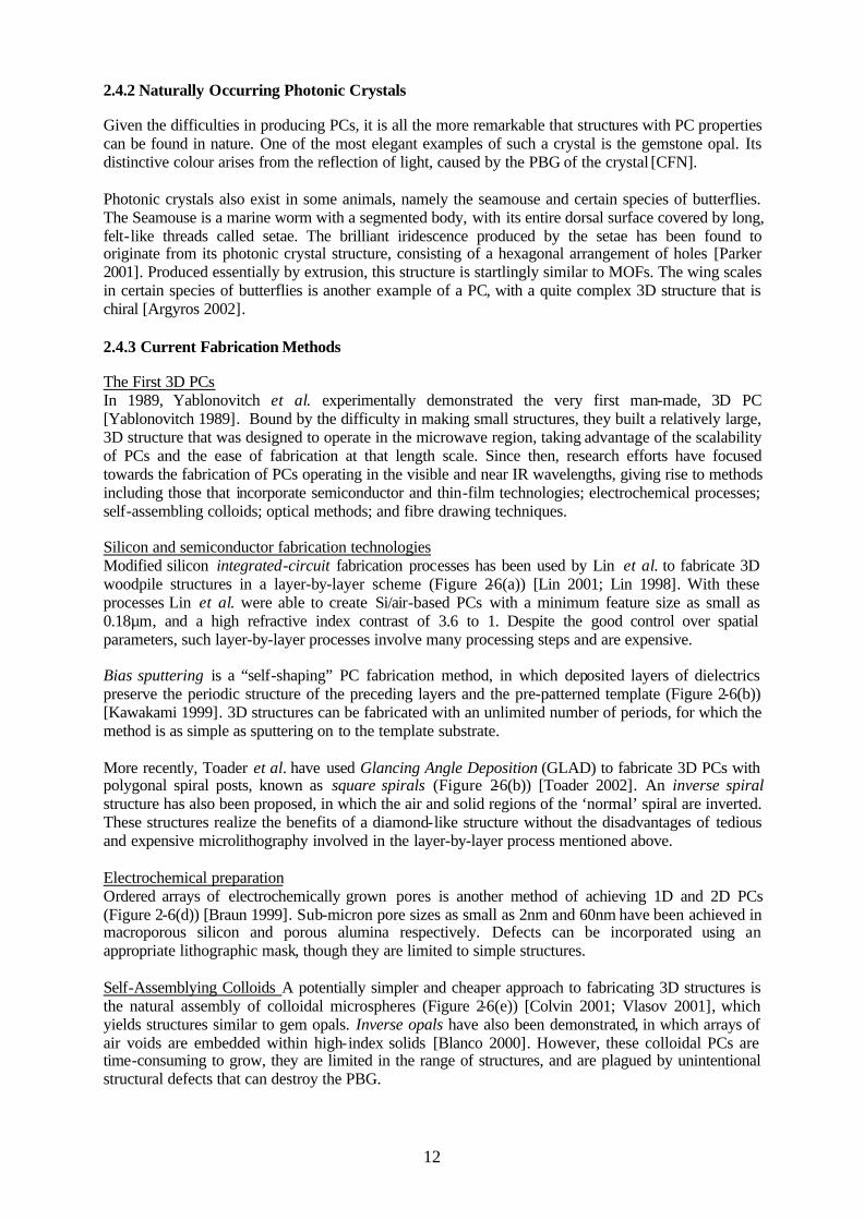
2.4.2 Naturally Occurring Photonic Crystals Given the difficulties in producing PCs, it is all the more remarkable that structures with PC properties can be found in nature. One of the most elegant examples of such a crystal is the gemstone opal. Its distinctive colour arises from the reflection of light, caused by the PBG of the crystal [CFN]. Photonic crystals also exist in some animals, namely the seamouse and certain species of butterflies. The Seamouse is a marine worm with a segmented body, with its entire dorsal surface covered by long, felt-like threads called setae. The brilliant iridescence produced by the setae has been found to originate from its photonic crystal structure, consisting of a hexagonal arrangement of holes [Parker 2001]. Produced essentially by extrusion, this structure is startlingly similar to MOFs. The wing scales in certain species of butterflies is another example of a PC, with a quite complex 3D structure that is chiral [Argyros 2002]. 2.4.3 Current Fabrication Methods The First 3D PCs In 1989, Yablonovitch et al. experimentally demonstrated the very first man-made, 3D PC [Yablonovitch 1989]. Bound by the difficulty in making small structures, they built a relatively large, 3D structure that was designed to operate in the microwave region, taking advantage of the scalability of PCs and the ease of fabrication at that length scale. Since then, research efforts have focused towards the fabrication of PCs operating in the visible and near IR wavelengths, giving rise to methods including those that incorporate semiconductor and thin-film technologies; electrochemical processes; self-assembling colloids; optical methods; and fibre drawing techniques. Silicon and semiconductor fabrication technologies Modified silicon integrated-circuit fabrication processes has been used by Lin et al. to fabricate 3D woodpile structures in a layer-by-layer scheme (Figure 2-6(a)) [Lin 2001; Lin 1998]. With these processes Lin et al. were able to create Si/air-based PCs with a minimum feature size as small as 0.18µm, and a high refractive index contrast of 3.6 to 1. Despite the good control over spatial parameters, such layer-by-layer processes involve many processing steps and are expensive. Bias sputtering is a “self-shaping” PC fabrication method, in which deposited layers of dielectrics preserve the periodic structure of the preceding layers and the pre-patterned template (Figure 2-6(b)) [Kawakami 1999]. 3D structures can be fabricated with an unlimited number of periods, for which the method is as simple as sputtering on to the template substrate. More recently, Toader et al. have used Glancing Angle Deposition (GLAD) to fabricate 3D PCs with polygonal spiral posts, known as square spirals (Figure 2-6(b)) [Toader 2002]. An inverse spiral structure has also been proposed, in which the air and solid regions of the ‘normal’ spiral are inverted. These structures realize the benefits of a diamond-like structure without the disadvantages of tedious and expensive microlithography involved in the layer-by-layer process mentioned above. Electrochemical preparation Ordered arrays of electrochemically grown pores is another method of achieving 1D and 2D PCs (Figure 2-6(d)) [Braun 1999]. Sub-micron pore sizes as small as 2nm and 60nm have been achieved in macroporous silicon and porous alumina respectively. Defects can be incorporated using an appropriate lithographic mask, though they are limited to simple structures. Self-Assemblying Colloids A potentially simpler and cheaper approach to fabricating 3D structures is the natural assembly of colloidal microspheres (Figure 2-6(e)) [Colvin 2001; Vlasov 2001], which yields structures similar to gem opals. Inverse opals have also been demonstrated, in which arrays of air voids are embedded within high-index solids [Blanco 2000]. However, these colloidal PCs are time-consuming to grow, they are limited in the range of structures, and are plagued by unintentional structural defects that can destroy the PBG.
13
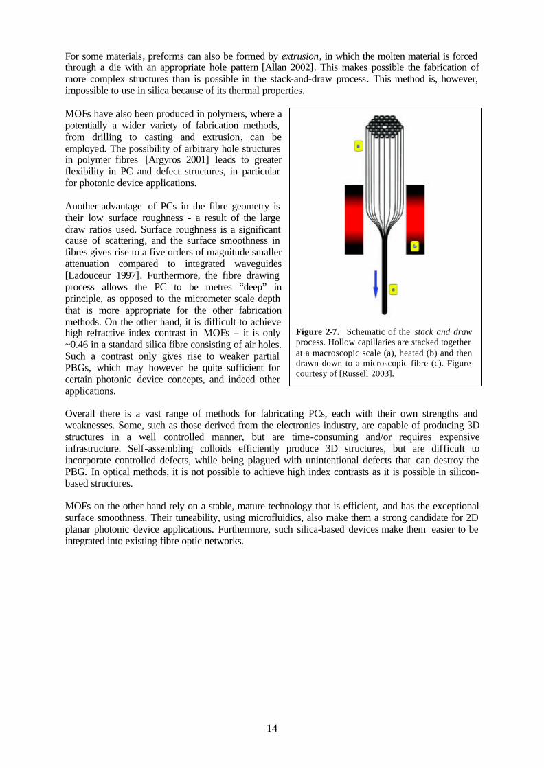
A potentially simpler and cheaper approach to fabricating 3D structures is the natural assembly of colloidal microspheres (Figure 2-6(e)) [Colvin 2001; Vlasov 2001] , which yields structures similar to gem opals. Inverse opals have also been demonstrated, in which arrays of air voids are embedded within high-index solids [Blanco 2000]. However, these colloidal PCs are time-consuming to grow, they are limited in the range of structures, and are plagued by unintentional structural defects that can destroy the PBG. Optical Methods PCs can also be fabricated by optical methods such as two-photon photopolymerization, where the interference of two laser beams is used to polymerize photosensitive precursor (Figure 2-6(f)) [Straub 2002; Sun 1999]. Despite the time-consumption, this point-by-point process allows for the fabrication of arbitrary structures. Alternatively, holographic lithography allows for the simultaneous construction of the entire crystal [Turberfield 2001]. The substrate is exposed only once to a 3D interference pattern in single exposure lithography [Campbell 2000], while in multiple exposure lithography, a two-step exposure to separate, orthogonal 2D and 1D patterns is used [Shoji 2000]. Despite the efficient fabrication process, the polymer-based photosensitive precursor only yields a relatively small refractive index contrast. Fibre Drawing Techniques 3D PCs allow ultimate control over the flow of light. However, this is often not necessary for applications in planar devices. 2D PCs provide sufficient control in such cases, and optical fibre drawing techniques are a method of fabricating such structures in MOFs, with numerous advantages. There are two common methods of fabricating Silica MOFs. First is the stack-and-draw process (Figure 2-7), in which glass capillaries are stacked together and drawn at high temperature, essentially fusing the rods into a single fibre consisting of longitudinal holes [Knight 1996; Knight 1997]. Amazingly, the centimeter-scale hexagonal hole structure in the preform is preserved during this process, and overall collapse ratios as large as ~50,000 times and holes as small as 25 nm have been realized so far [Russell 2003].
Figure 2-6. Examples of PC structures fabricated by integrated-circuit fabrication techniques (a) [Lin 1998]; bias sputtering (b) [Kawakami 1997]; GLAD (c) [John 2001]; electrochemical process (d) [Braun 1999]; self-assemblying colloids (e) [Vlasov 2001]; and two -photon photopolymerisation (f) [Straub 2002].
(a)
(b) (c)
(d) (e) (f)
14
For some materials, preforms can also be formed by extrusion, in which the molten material is forced through a die with an appropriate hole pattern [Allan 2002]. This makes possible the fabrication of more complex structures than is possible in the stack-and-draw process. This method is, however, impossible to use in silica because of its thermal properties. MOFs have also been produced in polymers, where a potentially a wider variety of fabrication methods, from drilling to casting and extrusion, can be employed. The possibility of arbitrary hole structures in polymer fibres [Argyros 2001] leads to greater flexibility in PC and defect structures, in particular for photonic device applications. Another advantage of PCs in the fibre geometry is their low surface roughness - a result of the large draw ratios used. Surface roughness is a significant cause of scattering, and the surface smoothness in fibres gives rise to a five orders of magnitude smaller attenuation compared to integrated waveguides [Ladouceur 1997]. Furthermore, the fibre drawing process allows the PC to be metres “deep” in principle, as opposed to the micrometer scale depth that is more appropriate for the other fabrication methods. On the other hand, it is difficult to achieve high refractive index contrast in MOFs – it is only ~0.46 in a standard silica fibre consisting of air holes. Such a contrast only gives rise to weaker partial PBGs, which may however be quite sufficient for certain photonic device concepts, and indeed other applications. Overall there is a vast range of methods for fabricating PCs, each with their own strengths and weaknesses. Some, such as those derived from the electronics industry, are capable of producing 3D structures in a well controlled manner, but are time-consuming and/or requires expensive infrastructure. Self-assembling colloids efficiently produce 3D structures, but are difficult to incorporate controlled defects, while being plagued with unintentional defects that can destroy the PBG. In optical methods, it is not possible to achieve high index contrasts as it is possible in silicon-based structures. MOFs on the other hand rely on a stable, mature technology that is efficient, and has the exceptional surface smoothness. Their tuneability, using microfluidics, also make them a strong candidate for 2D planar photonic device applications. Furthermore, such silica-based devices make them easier to be integrated into existing fibre optic networks.
Figure 2-7. Schematic of the stack and draw process. Hollow capillaries are stacked together at a macroscopic scale (a), heated (b) and then drawn down to a microscopic fibre (c). Figure courtesy of [Russell 2003].
38
References Allan, D. C., J. A. West, J. C. Fajardo, M. T. Gallagher, K. W. Koch and N. F. Borrelli (2002).
Photonic crystal fibers: effective-index and band-gap guidance. Photonic Crystals and Light Localization in the 21st Century. C. M. Soukoulis: 305-320.
Argyros, A., I. M. Bassett, M. A. van Eijkelenborg, M. C. J. Large, J. Zagari, N. A. P. Nicorovici, R. C. McPhedran and C. M. de Sterke (2001). "Ring structures in microstructured polymer optical fibres." Optics Express 9(13): 813-820.
Argyros, A., S. Manos, M. C. J. Large, D. R. McKenzie, G. C. Cox and D. M. Dwarte (2002). "Electron tomography and computer visualisation of a three-dimensional 'photonic' crystal in a butterfly wing-scale." Micron 33(5): 483-487.
Birks, T. A., J. C. Knight and P. S. Russell (1997). "Endlessly single -mode photonic crystal fiber." Optics Letters 22(13): 961-963.
Bjarklev, A., J. Broeng and A. S. Bjarklev (2003). Photonic Crystal Fibres. Blanco, A., E. Chomski, S. Grabtchak, M. Ibisate, S. John, S. W. Leonard, C. Lopez, F. Meseguer, H.
Miguez, J. P. Mondia, G. A. Ozin, O. Toader and H. M. van Driel (2000). "Large-scale synthesis of a silicon photonic crystal with a complete three-dimensional bandgap near 1.5 micrometres." Nature 405(6785): 437-440.
Botten, L. C., A. A. Asatryan, T. N. Langtry, T. P. White, C. M. de Sterke and R. C. McPhedran (2003). "Semianalytic treatment for propagation in finite photonic crystal waveguides." Optics Letters 28(10): 854-856.
Braun, P. V. and P. Wiltzius (1999). "Microporous materials - Electrochemically grown photonic crystals." Nature 402(6762): 603-604.
Campbell, M., D. N. Sharp, M. T. Harrison, R. G. Denning and A. J. Turberfield (2000). "Fabrication of photonic crystals for the visible spectrum by holographic lithography." Nature 404(6773): 53-56.
CFN. http://rryoo.kaist.ac.kr/res-3.html. Chen, L., Y. Suzuki and G. E. Kohnke (2002). "Integrated platform for silicon photonic crystal devices
at near-infrared wavelengths." Applied Physics Letters 80(9): 1514-1516. Colvin, V. L. (2001). "From opals to optics: Colloidal photonic crystals." Mrs Bulletin 26(8): 637-641. Cregan, R. F., B. J. Mangan, J. C. Knight, T. A. Birks, P. S. Russell, P. J. Roberts and D. C. Allan
(1999). "Single-mode photonic band gap guidance of light in air." Science 285(5433): 1537-1539.
Ho, K. M., C. T. Chan and C. M. Soukoulis (1990). "Existence of a Photonic Gap in Periodic Dielectric Structures." Physical Review Letters 65(25): 3152-3155.
Joannopoulos, J. D., R. D. Meade and J. N. Winn (1995). Photonic Crystals: Molding the Flow of Light, Princeton University Press.
John, S. (1987). "Strong Localization of Photons in Certain Disordered Dielectric Superlattices." Physical Review Letters 58(23): 2486-2489.
John, S. (2001). Photonic Band Gap Materials: A Semiconductor for Light.: Lecture given at the European Summer School Lectures 2001. Lecture slides accessed at: http://www.physics.utoronto.ca/~john/john/PBG.pdf. Last accessed 21/7/2003.
Kawakami, S. (1997). "Fabrication of submicrometre 3D periodic structures composed of Si/SiO2." Electronics Letters 33(14): 1260-1261.
Kawakami, S., T. Kawashima and T. Sato (1999). "Mechanism of shape formation of three-dimensional periodic nanostructures by bias sputtering." Applied Physics Letters 74(3): 463-465.
Knight, J. C., J. Arriaga, T. A. Birks, A. Ortigosa-Blanch, W. J. Wadsworth and P. S. Russell (2000). "Anomalous dispersion in photonic crystal fiber." Ieee Photonics Technology Letters 12(7): 807-809.
Knight, J. C., T. A. Birks, R. F. Cregan, P. S. Russell and J. P. de Sandro (1998). "Large mode area photonic crystal fibre." Electronics Letters 34(13): 1347-1348.
Knight, J. C., T. A. Birks, P. S. Russell and D. M. Atkin (1996). "All-silica single -mode optical fiber with photonic crystal cladding." Optics Letters 21(19): 1547-1549.
Knight, J. C., T. A. Birks, P. S. J. Russell and D. M. Atkin (1997). "All-silica single -mode optical fiber with photonic crystal cladding: Errata." Optics Letters 22(7): 484-485.
39
Knight, J. C., J. Broeng, T. A. Birks and P. S. J. Russel (1998). "Photonic band gap guidance in optical fibers." Science 282(5393): 1476-1478.
Kosaka, H., T. Kawashima, A. Tomita, M. Notomi, T. Tamamura, T. Sato and S. Kawakami (1999). "Photonic crystals for micro lightwave circuits using wavelength-dependent angular beam steering." Applied Physics Letters 74(10): 1370-1372.
Kosaka, H., T. Kawashima, A. Tomita, M. Notomi, T. Tamamura, T. Sato and S. Kawakami (1999). "Superprism phenomena in photonic crystals: Toward microscale lightwave circuits." Journal of Lightwave Technology 17(11): 2032-2038.
Ladouceur, F. (1997). "Roughness, inhomogeneity, and integrated optics." Journal of Lightwave Technology 15(6): 1020-1025.
Lin, S. Y., E. Chow, V. Hietala, P. R. Villeneuve and J. D. Joannopoulos (1998). "Experimental demonstration of guiding and bending of electromagnetic waves in a photonic crystal." Science 282(5387): 274-276.
Lin, S. Y., J. G. Fleming and E. Chow (2001). "Two- and three-dimensional photonic crystals built with VLSI tools." Mrs Bulletin 26(8): 627-631.
Lin, S. Y., J. G. Fleming, D. L. Hetherington, B. K. Smith, R. Biswas, K. M. Ho, M. M. Sigalas, W. Zubrzycki, S. R. Kurtz and J. Bur (1998). "A three-dimensional photonic crystal operating at infrared wavelengths." Nature 394(6690): 251-253.
Lin, S. Y., J. G. Fleming, D. L. Hetherington, B. K. Smith, R. Biswas, K. M. Ho, M. M. Sigalas, W. Zubrzycki, S. R. Kurtz and J. Bur (1998). "A three-dimensional photonic crystal operating at infrared wavelengths." Nature vol.394, no.6690: 251-253.
Loncar, M., T. Doll, J. Vuckovic and A. Scherer (2000). "Design and fabrication of silicon photonic crystal optical waveguides." Journal of Lightwave Technology 18(10): 1402-1411.
Mach, P., M. Dolinski, K. W. Baldwin, J. A. Rogers, C. Kerbage, R. S. Windeler and B. J. Eggleton (2002). "Tunable microfluidic optical fiber." Applied Physics Letters 80(23): 4294-4296.
Meade, R. D., A. Devenyi, J. D. Joannopoulos, O. L. Alerhand, D. A. Smith and K. Kash (1994). "Novel Applications of Photonic Band-Gap Materials - Low-Loss Bends and High Q-Cavit ies." Journal of Applied Physics 75(9): 4753-4755.
Mekis, A., J. C. Chen, I. Kurland, S. H. Fan, P. R. Villeneuve and J. D. Joannopoulos (1996). "High transmission through sharp bends in photonic crystal waveguides." Physical Review Letters 77(18): 3787-3790.
Neumann, E.-G., 1929- (c1988.). Single-mode fibers : fundamentals / E.-G. Neumann. Berlin ; New York :, Springer,.
Painter, O., R. K. Lee, A. Scherer, A. Yariv, J. D. O'Brien, P. D. Dapkus and I. Kim (1999). "Two-dimensional photonic band-gap defect mode laser." Science 284(5421): 1819-1821.
Parker, A. R., R. C. McPhedran, D. R. McKenzie, L. C. Botten and N. A. P. Nicorovici (2001). "Photonic engineering - Aphrodite's iridescence." Nature 409(6816): 36-37.
Rayleigh, L. (1887). "On the maintenance of vibrations by forces of double frequency, and on the propagation of waves through a medium endowed with a periodic structure." Philosophical Magazine 24: 145-159.
RSoft Design Group, I. (2003). BandSOLVETM 1.2.0 User Guide. RSoft Design Group, I. (2003). FullWAVETM 3.0.1 User Guide. Russell, P. (2003). "Photonic crystal fibers." Science 299(5605): 358-362. Scarmozzino, R., A. Gopinath, R. Pregla and S. Helfert (2000). "Numerical techniques for modeling
guided-wave photonic devices." Ieee Journal of Selected Topics in Quantum Electronics 6(1): 150-162.
Shoji, S. and S. Kawata (2000). "Photofabrication of three-dimensional photonic crystals by multibeam laser interference into a photopolymerizable resin." Applied Physics Letters 76(19): 2668-2670.
Straub, M. and M. Gu (2002). "Near-infrared photonic crystals with higher-order bandgaps generated by two-photon photopolymerization." Optics Letters 27(20): 1824-1826.
Sun, H. B., S. Matsuo and H. Misawa (1999). "Three-dimensional photonic crystal structures achieved with two-photon-absorption photopolymerization of resin." Applied Physics Letters 74(6): 786-788.
Toader, O. and S. John (2002). "Square spiral photonic crystals: Robust architecture for microfabrication of materials with large three-dimensional photonic band gaps." Physical Review E 66(1).

40
Turberfield, A. J. (2001). "Photonic crystals made by holographic lithography." Mrs Bulletin 26(8): 632-636.
Vlasov, Y. A., X. Z. Bo, J. C. Sturm and D. J. Norris (2001). "On-chip natural assembly of silicon photonic bandgap crystals." Nature 414(6861): 289-293.
Yablonovitch, E. (1987). "Inhibited Spontaneous Emission in Solid-State Physics and Electronics." Physical Review Letters 58(20): 2059-2062.
Yablonovitch, E. and T. J. Gmitter (1989). "Photonic Band-Structure - the Face-Centered-Cubic Case." Physical Review Letters 63(18): 1950-1953.
Zijlstra, T., E. van der Drift, M. J. A. de Dood, E. Snoeks and A. Polman (1999). "Fabrication of two-dimensional photonic crystal waveguides for 1.5 mu m in silicon by deep anisotropic dry etching." Journal of Vacuum Science & Technology B 17(6): 2734-2739.


![Symmetry Classification of Topological Photonic Crystals ... · arXiv:1710.08104v2 [physics.optics] 6 Dec 2017 Symmetry Classification of Topological Photonic Crystals Giuseppe](https://img.pdfslide.us/doc/110x75/5e485a76f7f1722c7d42dc37/symmetry-classiication-of-topological-photonic-crystals-arxiv171008104v2.jpg)