Embed Size (px)
Citation preview

Photonic Links -- From Theory to Automated Design
Krishna Settaluri
Electrical Engineering and Computer SciencesUniversity of California at Berkeley
Technical Report No. UCB/EECS-2019-8http://www2.eecs.berkeley.edu/Pubs/TechRpts/2019/EECS-2019-8.html
April 23, 2019

Copyright © 2019, by the author(s).All rights reserved.
Permission to make digital or hard copies of all or part of this work forpersonal or classroom use is granted without fee provided that copies arenot made or distributed for profit or commercial advantage and that copiesbear this notice and the full citation on the first page. To copy otherwise, torepublish, to post on servers or to redistribute to lists, requires prior specificpermission.
Acknowledgement
This PhD came at a very opportune time in my life. On the one hand, I beganthis journey with a more refined sense of judgment, thought, and knowledgethan, say, when I entered undergrad. On the other, I still consider myselfyoung enough to mold, adapt, and grow to the people and environmentaround me. Putting that together, the people I bonded with during the lastfive years are special in not only being unique, exceptionally talented, loving,and hilarious but also having the ability to teach and change me for thebetter.

Photonic Links – From Theory to Automated Design
by
Krishna Tej Settaluri
A dissertation submitted in partial satisfaction of the
requirements for the degree of
Doctor of Philosophy
in
Engineering - Electrical Engineering and Computer Sciences
in the
Graduate Division
of the
University of California, Berkeley
Committee in charge:
Professor Vladimir Stojanovic, ChairProfessor Eli Yablonovitch
Professor Costas Grigoropoulos
Fall 2018

Photonic Links – From Theory to Automated Design
Copyright c© 2018
by
Krishna Tej Settaluri

1
Abstract
Photonic Links – From Theory to Automated Design
by
Krishna Tej SettaluriDoctor of Philosophy in Engineering - Electrical Engineering and Computer Sciences
University of California, BerkeleyProfessor Vladimir Stojanovic, Chair
Recent advancements in silicon photonics show great promise in meeting the highbandwidth and low energy demands of emerging applications. However, a key gatingfactor in ensuring this necessity is met is the utilization of a link design method-ology which transcends the various levels in the hierarchy, ranging from the deviceand platform level up to the systems level. In this dissertation, a comprehensivemethodology for link design will be introduced which takes a two-prong approach totackling the issue of silicon photonic link efficiency. Namely, a fundamentals-basedfirst principles approach to link optimization will be introduced and validated. Inaddition, physical design trade-offs connecting levels in the architectural hierarchywill also be studied and explored. This culminates in an intermediate goal of thisdissertation, which is the first-ever design and verification of a full silicon photonicinterconnect on a 3D integrated electronic-photonic platform. To proceed and furtherenable the rapid exploration of the link design architectural space, the analog macrosfor a majority of this dissertation were auto-generated using the Berkeley Analog Gen-erator (BAG). With these key design tools and framework, performance bottlenecksand improvements for silicon photonic links will be analyzed and, from this analysis,the motivation for a new, single comparator-based PAM4 receiver architecture shallemerge. This architecture not only showcases the tight bond in dependency betweenhigh-level link specifications and low level device parameters, but also shows the im-portance of physical design constraints alongside fundamental theory in influencingend-to-end link performance.

i
To Mom and Dad.

ii
Contents
Contents ii
List of Figures v
List of Tables ix
1 Introduction 1
2 Background 32.1 Silicon Photonic Links . . . . . . . . . . . . . . . . . . . . . . . . . . 3
2.1.1 Photonic Building Blocks . . . . . . . . . . . . . . . . . . . . . 42.1.2 Optical Communication Links . . . . . . . . . . . . . . . . . . 62.1.3 Circuit Design Challenges and Methodology . . . . . . . . . . 7
2.2 Silicon Photonic Integration Platforms . . . . . . . . . . . . . . . . . 72.2.1 3D Integration Using Thru-Oxide Vias . . . . . . . . . . . . . 82.2.2 3D Integration Using Flip Chip µBumps . . . . . . . . . . . . 8
2.3 Analog Circuit Design Challenges and Automation . . . . . . . . . . 92.3.1 BAG Architecture and Flow . . . . . . . . . . . . . . . . . . . 9
2.4 Conclusion . . . . . . . . . . . . . . . . . . . . . . . . . . . . . . . . . 13
3 End-to-End Optical Link Design Methodology 153.1 Introduction . . . . . . . . . . . . . . . . . . . . . . . . . . . . . . . . 153.2 Optical Link Modeling . . . . . . . . . . . . . . . . . . . . . . . . . . 17
3.2.1 High-Level Receiver Abstraction . . . . . . . . . . . . . . . . . 173.2.2 Gain-Bandwidth product . . . . . . . . . . . . . . . . . . . . . 183.2.3 Voltage Amplifiers . . . . . . . . . . . . . . . . . . . . . . . . 183.2.4 Transimpedance Amplifier . . . . . . . . . . . . . . . . . . . . 193.2.5 Sampler Model in Receiver . . . . . . . . . . . . . . . . . . . . 20
3.3 Macro-Parameter Derivations . . . . . . . . . . . . . . . . . . . . . . 253.3.1 Sensitivity calculation . . . . . . . . . . . . . . . . . . . . . . 253.3.2 Energy per bit . . . . . . . . . . . . . . . . . . . . . . . . . . . 263.3.3 Model inputs and optimization variables . . . . . . . . . . . . 29

iii
3.3.4 Model purpose and limitations . . . . . . . . . . . . . . . . . . 293.4 Sensitivity and energy limits . . . . . . . . . . . . . . . . . . . . . . . 29
3.4.1 Front end noise limit . . . . . . . . . . . . . . . . . . . . . . . 293.4.2 Limits at high data rates . . . . . . . . . . . . . . . . . . . . . 313.4.3 Limits at low datarates . . . . . . . . . . . . . . . . . . . . . . 313.4.4 E/b power laws . . . . . . . . . . . . . . . . . . . . . . . . . . 32
3.5 Observations in Scaling and Technology . . . . . . . . . . . . . . . . . 323.5.1 Improvements in Photonics and Interconnects . . . . . . . . . 333.5.2 Improvements in Photonics+CMOS . . . . . . . . . . . . . . . 33
3.6 Link Framework and First-Principles Summary . . . . . . . . . . . . 363.7 Conclusion . . . . . . . . . . . . . . . . . . . . . . . . . . . . . . . . . 36
4 Link Framework Application for NRZ Front-End Design 384.1 Introduction . . . . . . . . . . . . . . . . . . . . . . . . . . . . . . . . 384.2 Model Application for 65nm Heterogenously Integrated Photonic Plat-
form . . . . . . . . . . . . . . . . . . . . . . . . . . . . . . . . . . . . 394.2.1 Technology overview . . . . . . . . . . . . . . . . . . . . . . . 394.2.2 Single slicer case (M=1) . . . . . . . . . . . . . . . . . . . . . 394.2.3 Multiple slicer case (M ≥ 1) . . . . . . . . . . . . . . . . . . . 40
4.3 Schematic designs of model results . . . . . . . . . . . . . . . . . . . 424.3.1 5Gbps optical receiver . . . . . . . . . . . . . . . . . . . . . . 424.3.2 Active-CTLE enhanced 5Gbps optical receiver . . . . . . . . . 434.3.3 DDR 25Gbps optical receiver . . . . . . . . . . . . . . . . . . 444.3.4 QDR 25Gbps optical receiver . . . . . . . . . . . . . . . . . . 464.3.5 Switched QDR 25Gbps optical receiver . . . . . . . . . . . . . 47
4.4 Conclusion . . . . . . . . . . . . . . . . . . . . . . . . . . . . . . . . . 48
5 3D Integrated Silicon Photonic Interconnects 495.1 Introduction . . . . . . . . . . . . . . . . . . . . . . . . . . . . . . . . 495.2 Overview . . . . . . . . . . . . . . . . . . . . . . . . . . . . . . . . . . 505.3 3D Integration of CMOS and Photonics . . . . . . . . . . . . . . . . . 515.4 Chip Architecture and Optical Link System . . . . . . . . . . . . . . 52
5.4.1 Transmitter Design . . . . . . . . . . . . . . . . . . . . . . . . 535.4.2 Receiver Design . . . . . . . . . . . . . . . . . . . . . . . . . . 555.4.3 Thermal Tuner Design . . . . . . . . . . . . . . . . . . . . . . 575.4.4 Link Implementation and Test setup . . . . . . . . . . . . . . 57
5.5 Conclusion . . . . . . . . . . . . . . . . . . . . . . . . . . . . . . . . . 59
6 Single-Comparator PAM4 Architecture 636.1 Introduction . . . . . . . . . . . . . . . . . . . . . . . . . . . . . . . . 636.2 PAM4 Introduction and Link Trade-Offs . . . . . . . . . . . . . . . . 636.3 Single Comparator PAM4 Receiver . . . . . . . . . . . . . . . . . . . 67

iv
6.3.1 Motivation . . . . . . . . . . . . . . . . . . . . . . . . . . . . . 686.3.2 Proposed Architecture and Formulation . . . . . . . . . . . . . 696.3.3 Design Methodology and Theoretical Performance . . . . . . . 746.3.4 End-to-End Photonic Co-Simulation Results . . . . . . . . . . 79
6.4 Conclusion . . . . . . . . . . . . . . . . . . . . . . . . . . . . . . . . . 81
7 Acacia System Design 837.1 Introduction . . . . . . . . . . . . . . . . . . . . . . . . . . . . . . . . 837.2 Acacia System Design . . . . . . . . . . . . . . . . . . . . . . . . . . 83
7.2.1 Front-End Floorplanning and PDK Generation Constraints . . 837.2.2 Receiver AFE Design and Insights . . . . . . . . . . . . . . . . 917.2.3 Transmitter Design and Automation . . . . . . . . . . . . . . 927.2.4 New Transmit-Side Thermal Tuning . . . . . . . . . . . . . . 937.2.5 Tx-Rx Self Test Setup . . . . . . . . . . . . . . . . . . . . . . 947.2.6 Putting together the Acacia System . . . . . . . . . . . . . . . 95
7.3 Results . . . . . . . . . . . . . . . . . . . . . . . . . . . . . . . . . . . 967.3.1 On-Chip Clock Network . . . . . . . . . . . . . . . . . . . . . 967.3.2 Rx AFE and Self Test Characterization . . . . . . . . . . . . . 987.3.3 25.6Gbps Self Test Link . . . . . . . . . . . . . . . . . . . . . 99
7.4 Conclusion . . . . . . . . . . . . . . . . . . . . . . . . . . . . . . . . . 99
8 Conclusion 1018.1 Thesis Contributions . . . . . . . . . . . . . . . . . . . . . . . . . . . 1018.2 Future Work and Final Thoughts . . . . . . . . . . . . . . . . . . . . 102
Bibliography 103

v
List of Figures
2.1 The microring modulator enables OOK encoding while also enablingwavelength selectivity. . . . . . . . . . . . . . . . . . . . . . . . . . . 4
2.2 The photodetector is responsible for generating an output current de-pendent on the input optical power. . . . . . . . . . . . . . . . . . . . 6
2.3 A WDM link composed of many transmit and receive side rings is anattractive solution which allows high bandwidth density. . . . . . . . 7
2.4 A cross section and top view of the TOV are shown. . . . . . . . . . . 82.5 The design flow of a new block within the BAG framework is shown. 92.6 The design flow with feedback from the output of simulations enables
rapid iteration. [4] . . . . . . . . . . . . . . . . . . . . . . . . . . . . . 102.7 The schematic, transient, and example floorplan of the StrongArm is
shown. . . . . . . . . . . . . . . . . . . . . . . . . . . . . . . . . . . . 112.8 The output of the schematic and layout generators produce DRC and
LVS clean instances of the StrongArm. . . . . . . . . . . . . . . . . . 122.9 The framework allows for push-button instantiation and verification to
generate quick, correct instances. . . . . . . . . . . . . . . . . . . . . 122.10 Pushing an instance through a full design flow is simple within this
codified environment. . . . . . . . . . . . . . . . . . . . . . . . . . . . 13
3.1 Demonstrated Optical Link Efficiencies [6-15], Against Objectives From[6]. Further information at linksurvey.eecs.berkeley.edu. . . . . . . . . 16
3.2 Optical Link System Overview . . . . . . . . . . . . . . . . . . . . . . 163.3 StrongArm Sampler Schematic . . . . . . . . . . . . . . . . . . . . . . 203.4 Sampler Timing Evaluation Breakdown . . . . . . . . . . . . . . . . . 233.5 Ideal Transfer Function of A System with Equalization . . . . . . . . 303.6 Technology Dependent Performance Prediction . . . . . . . . . . . . . 36
4.1 Optimal Energy Per Bit Versus Data rate For Optimal Topologies WithParameters From Table 3.1. Only One Slicer is Allowed in This Case 40
4.2 Optimal Energy Per Bit Versus Data rate For Optimal Topologies WithParameters from Table 3.1 with the Possibility of Multiple Slicers . . 41
4.3 5Gbps Receiver Topology . . . . . . . . . . . . . . . . . . . . . . . . . 42

LIST OF FIGURES vi
4.4 5Gbps Model-Predicted Receiver Topology with Active-CTLE . . . . 444.5 25Gbps Optical Receiver With Variable Interleaving Stages . . . . . . 454.6 Switching Time-Interleaved 25Gbps QDR Receiver . . . . . . . . . . 47
5.1 A comparison of the integration technology categories shows pros andcons for both. . . . . . . . . . . . . . . . . . . . . . . . . . . . . . . . 50
5.2 An example diagram of the full WDM link using a heterogeneous plat-form shows independent photonic and CMOS wafers on both the Txand Rx side. . . . . . . . . . . . . . . . . . . . . . . . . . . . . . . . . 51
5.3 A cross section of the 3D TOV heterogeneous integration process showsthe photonic and CMOS wafers and associated connections. . . . . . 52
5.4 A full system of the heterogeneously integrated EPHI system. . . . . 535.5 The Tx Macro consists of high speed serializers and drivers shift the
ring resonance. . . . . . . . . . . . . . . . . . . . . . . . . . . . . . . 545.6 The Tx microring resonance characteristics and eye diagrams are shown. 555.7 The receiver AFE as well as the photodiode is shown. . . . . . . . . . 555.8 The Rx photonic ring responsivitity and response versus frequency. . 565.9 Measured receiver average photo-current sensitivity over different data
rates and BER bathtub curves for both receiver slices. . . . . . . . . . 575.10 The thermal tuner block diagram used to control the microring reso-
nance is shown. . . . . . . . . . . . . . . . . . . . . . . . . . . . . . . 585.11 The progression of the transient eye along with the resonance location
for the thermal tuner. . . . . . . . . . . . . . . . . . . . . . . . . . . . 595.12 The test setup of the EPHI chip contains the Tx and Rx macros con-
nected by a 100m fiber reel. . . . . . . . . . . . . . . . . . . . . . . . 605.13 Full optical link with optical power budget and performance. . . . . . 615.14 Electrical energy breakdown for the Tx and Rx macros in a 5Gb/s link. 625.15 Comparison with previous work. . . . . . . . . . . . . . . . . . . . . . 62
6.1 The traditional PAM4 architecture comprises of three comparators af-ter the AFE to slice the 4-level eye. . . . . . . . . . . . . . . . . . . . 64
6.2 Removing all constraints on the receiver architecture shows that thePAM4 architecture is superior to NRZ under particular system con-straints. . . . . . . . . . . . . . . . . . . . . . . . . . . . . . . . . . . 65
6.3 A comparison of the E/b for a PAM4 versus NRZ link comprised ofonly a single interleaving way for slicing shows the benefits of PAM4over NRZ. . . . . . . . . . . . . . . . . . . . . . . . . . . . . . . . . . 66
6.4 A comparison of the E/b for a PAM4 versus NRZ link comprised ofonly a single comparator for slicing shows the benefits of PAM4 overNRZ. . . . . . . . . . . . . . . . . . . . . . . . . . . . . . . . . . . . . 67
6.5 Full, end-to-end drawing of the photonic link along with a point to thecritical node – the primary concern of this chapter. . . . . . . . . . . 68

LIST OF FIGURES vii
6.6 Preliminary link performance results show the benefit of scaling downthe sampler capacitance by 3×. . . . . . . . . . . . . . . . . . . . . . 69
6.7 Behavior of a PAM4 receiver with a single comparator yield “NRZ-equivalent” behavior. . . . . . . . . . . . . . . . . . . . . . . . . . . . 70
6.8 The StrongArm Sense Amplifier schematic along with two sets of wave-forms (red and green) showing the output due to a large and small inputsignal, respectively. . . . . . . . . . . . . . . . . . . . . . . . . . . . . 70
6.9 A fully differential PAM4 front-end will have two complementary out-puts centered about the common-mode. . . . . . . . . . . . . . . . . . 72
6.10 A time-to-digital circuit takes an input the differential outputs of theStrongArm sense amplifier. . . . . . . . . . . . . . . . . . . . . . . . . 73
6.11 The sample waveforms of the TDC block show pulse width’s depen-dency on the output StrongArm waveforms. . . . . . . . . . . . . . . 73
6.12 The TDC receiver architecture composed of the AFE and a single in-terleaving way composed of the StrongArm, D2S, and new TDC (fromFigure 6.10). . . . . . . . . . . . . . . . . . . . . . . . . . . . . . . . . 74
6.13 Non-idealities in the AFE result in a voltage ratio between the BigBitand LittleBit that is smaller than theoretical 3×. . . . . . . . . . . . 76
6.14 The double tail sense amplifier has benefits in the new PAM4 contextthat outweigh the traditional StrongArm sense amplifier. . . . . . . . 77
6.15 The double tail sense amplifier evaluation-time “gain” may be charac-terized using Equations 6.9 and 6.10. The MATLAB simulation resultsare plotted here. . . . . . . . . . . . . . . . . . . . . . . . . . . . . . . 78
6.16 A comparison of the new, TDC-based PAM4 receiver and the tradi-tional, three-comparator architecture show the potential benefits whenviewing the link energy consumption. These results reflect not onlythe three-comparator difference, but also any secondary limitations ongm due to the presence of the TDC. . . . . . . . . . . . . . . . . . . . 80
6.17 The end-to-end photonic co-simulation schematic shows the Tx driver,photonic components, and the CMOS receiver. . . . . . . . . . . . . . 81
6.18 The receiver input current eye is shown. This signal was produced by aCMOS transmitter driving a photonic microring. The modulated lightgoes into a VerilogA photodiode to produce this eye. . . . . . . . . . 81
6.19 The output of the Rx AFE is shown. This signal subsequently traversesinto a single slicer prior to digitizing. . . . . . . . . . . . . . . . . . . 82
7.1 The AFE’s signal-critical blocks are placed first to ensure optimizedperformance and minimize path lengths and parasitics. . . . . . . . . 85
7.2 The full Rx front-end layout is composed of the signal-critical blocks,deserializers, and DACs. . . . . . . . . . . . . . . . . . . . . . . . . . 86

LIST OF FIGURES viii
7.3 The bumps (shown using the artistically rendered red squares) arespaced evenly, with the purpose of interposing with the componentson the photonic reticle. . . . . . . . . . . . . . . . . . . . . . . . . . . 87
7.4 Bump pitch variations result in very simple changes to the macro scriptin order to produce the two flavors of Rx above (drawn to scale relativeto one another). . . . . . . . . . . . . . . . . . . . . . . . . . . . . . . 88
7.5 Routing channels, although constrain the maximum width of the Rxfront-end, provide much needed space to allow proper routing betweenthe front-end digital bits and the digital backend. . . . . . . . . . . . 89
7.6 The body-connected and non-body connected transistor flavors arevastly different from the standpoint of the generator. This image showsthe two flavors, with similar widths and 5 fingers. . . . . . . . . . . . 90
7.7 The Rx AFE (simplified) schematic shows the main blocks along thecritical signal path. . . . . . . . . . . . . . . . . . . . . . . . . . . . . 91
7.8 The Tx-side AC driver uses a push/pull architecture to maximize thevoltage swing across the microring modulator. . . . . . . . . . . . . . 92
7.9 The closed loop thermal tuner serves to ensure that the microringresonance remains in lock. This scheme has the added benefit of notrequiring an additional drop-port. . . . . . . . . . . . . . . . . . . . . 93
7.10 The self test schematic shows the full data path to characterize theAFEs. . . . . . . . . . . . . . . . . . . . . . . . . . . . . . . . . . . . 94
7.11 The full Acacia system realizes a high speed, high performance end-to-end optical link with all necessary critical peripherals within thesystem. . . . . . . . . . . . . . . . . . . . . . . . . . . . . . . . . . . . 95
7.12 By modifying the capacitive DAC code, the output frequency of theglobal clock distribution can be modified according to the plot above. 97
7.13 The link’s performance is shown for low frequency and operating inMSB-mode. . . . . . . . . . . . . . . . . . . . . . . . . . . . . . . . . 98
7.14 The link’s performance is shown for low frequency and operating inMSB-mode. . . . . . . . . . . . . . . . . . . . . . . . . . . . . . . . . 99
7.15 The bathtub curve of the Acacia link operating at 25.6Gbps is shown. 100

ix
List of Tables
3.1 Model inputs and optimization variables . . . . . . . . . . . . . . . . 283.2 Minimum power laws for E/b limits dependence . . . . . . . . . . . . 333.3 Performance Comparison of Model-Predicted and Schematic-Simulated
Optical Receivers . . . . . . . . . . . . . . . . . . . . . . . . . . . . . 35
6.1 This table summarizes the alternate interpretation of the PAM encod-ing scheme, using a single comparator’s “timing information”. . . . . 72
LIST OF TABLES x
Acknowledgments
This PhD came at a very opportune time in my life. On the one hand, I beganthis journey with a more refined sense of judgment, thought, and knowledge than,say, when I entered undergrad. On the other, I still consider myself young enoughto mold, adapt, and grow to the people and environment around me. Putting thattogether, the people I bonded with during the last five years are special in not onlybeing unique, exceptionally talented, loving, and hilarious but also having the abilityto teach and change me for the better.
To begin, none of this would be possible without my advisor, Professor Sto-janovic. He gave me a chance and an opportunity to succeed at a time when I neededit the most. His knowledge was inspiring and his optimism has been the bane of myexistence for the last half decade. And, most recently, his incredible dance moveshave shown me that I have much to learn. Oh, and thanks for not caring about themany coffee-related issues in Cory.
During my PhD, I had the wonderful opportunity to engage with colleagues andfaculty members both inside and outside of the circuits space. Thanks to ProfessorEli Yablonovitch, whose brain-scratching questions left me dazed for days and toProfessor Ming Wu for valuable insight into the photonic-device space. To ChrisKeraly and Nicolas Andrade, thank you for your help refining and innovating the linkframework. To Professor Elad Alon, looking forward to our next adventure together.To Professor Ali Niknejad, I wish we could have played more soccer, but the timeswe did play were boundlessly fun. And, to Erman Timurdogan, Zhan Su, and ProfMichael Watts at MIT for support with EPHI and Acacia.
This thesis would not be possible without the kind, caring direction of my fellowBWRC lab mates. To begin, teamvlada has been an endless source of literally ev-erything. Sen Lin and Sajjad Moazeni have been my battle buddies throughout theyears. Nandish Mehta has been a loving, caring force of nature for many a tape-outs.Pavan Bhargava, you are my fiercest ally and friend. To the Acacia team composedof Sidney, Kourosh, Ruocheng, Zhaokai, Eric KJ, and Nick, I really hope you learneda great deal during the process and had as much ”fun” as I did. To Taehwan, Panos,and Christos thanks for your help and support over the years.
I would like to thank others at BWRC. Thank you to Greg and Luke who havenever changed and I sincerely hope never will. Your support and intimidatingly strongbackground in circuits has been beyond helpful. To Antonio and John, thank you foryour continued friendship and beards. To Bonjern, thanks for being the most excitedWarriors fan I know. Nathan, thanks also for the beard and coming to my wedding.Looking forward to what’s next. And thank you to Sameet, who was the best weddingofficiant a guy could ask for. You are hilarious, logical, sharp, and caring. I hopethere are no more pasta aglio e olios in our future.
Thank you to Chen, Mark, and Ranko for being fantastic mentors during myPhD. You have taught me many a lesson and I’m sure that that will continue.

xi
Thank you Candy for basically running the center, for providing granola, and forplants/life/food advice. To Ajith, Brian, Fred, Melissa, Olivia, Yessica, Erin, andLeslie thanks for being the backbone of this center.
To those outside of BWRC, thank you to Vinay (and James, I guess) for stillputting up with my incessant altitude humor. Thank you, Korok, for many fascinatingconversations and chin (not a typo). Thank you, Jasdeep and Pingy for TiddleWinklePingydinkle and so much more. Thanks to the Bandits for letting me never sub out ofball games. This might be a good time to also thank Twalve for his support and abilityto hold many many cars in his garage (and many hearts in his fish bowl). Thank youKevin, Katrina, Jorge, and Dani for continued support. To Pallovy, Abhiram, Jiwon,Susan, Ankush, Riley, Anusha (blabla), Josh Hsaio, and Lakshmi, thank you all forbeing there for me.
I would not be an iota of the person I am now today without my family. Tomy dad, Dr. Raghu Kumar Settaluri, and mom, Sandhya Rani Settaluri. You twoare jaw-droppingly inspiring and loving. Seriously, well done! To my dearest sister,Keertana. I’m so grateful to have you in my life and in BWRC. You will always havea special place in my heart, booboo.
Last, but certainly not least, thank you to my dearest wife, Pallavi. You havebeen a part of my life during all its ups and downs, yet you remain grounded, logical,and hilarious. I cannot think of a reality without you and I am endlessly in yourdebt. I am sure we have a lot more adventures to go on and I know we are readyfor anything. And I’ll be sure to take care of you anywhere we go – after all, I’m adoctor now.
-Krishna

1
Chapter 1
Introduction
With the recent increase in demand of high performance computing and withthe emergence of the 5G mobile market, global IP traffic has steadily increased overthe past 5 years and is projected to continue doing so for the foreseeable future.To meet these consumer communication bandwidth demands, modern data-centersand computers require optimization at every level in the system hierarchy. Siliconphotonics integration within large-scale systems-on-chip (SoCs) has emerged as aprimary contender in not only enhancing the capabilites of CMOS technologies, butalso meeting the high bandwidth and low energy demands of these next-generationcomputing interconnects. Recent years have seen great strides in the developmentand commercialization of silicon photonic technologies.
However, as complexity and performance of these systems ever increases, manyproblems still remain and numerous new ones emerge. Specifically, to continue op-timizing system efficiencies given new and ever changing process, technologies, anddevices, a unified framework needs to be in place to quickly characterize and explorethe design landscape. Moreover, to truly realize rapid design exploration, automationat every level in the hierarchy becomes mandatory – from high-level place and routeoptimization to low-level analog automation.
This thesis delves into optimizing the silicon photonic link performance by meansof two parallel thrusts. First, the optimization of performance shall be approachedby taking a fundamentals, theory-oriented approach. A link design framework whichis versatile in process, technology, and device will be introduced in Chapter 3. Thisframework allows for quick optimization contingent on the CMOS as well as pho-tonic parameters. From here, the validity of the framework will be further enforcedin Chapter 4, wherein particular design points for the 65nm heterogeneously inte-grated photonic platform will be selected and explored. This work was publishedin “First Principles Optimization of Opto-Electronic Communication Links” in theIEEE Transactions on Circuits and Systems I: Regular Papers [1]. The authors ofthis work were Krishna T. Settaluri, Christopher Lalau-Keraly, Eli Yablonovitch,Vladimir Stojanovic. The author of this dissertation contributed in developing the

CHAPTER 1. INTRODUCTION 2
theory and methodology for the link design framework.In addition, transmit-side exploration will also take place with the utilization of
a new, nanoLED-based transmitter model. The nanoLED-based transmit work waspublished in “Optical Antenna nanoLED Based Interconnect Design” in the IEEE IPC2018 [2]. The authors of this work were Nicolas M. Andrade, Krishna T. Settaluri,Seth A. Fortuna, Sean Hooten, Kevin Han, Eli Yablonovitch, Vladimir Stojanovic,and Ming C. Wu. The author’s contribution to this work were in the form of theend-to-end link model incorporation with the nanoLED transmitter model.
Next, in Chapter 5, a detailed analysis and design of an end-to-end 5Gbps NRZlink will be introduced. Here, we get a taste of the full design flow or “package” whichcomes about from aiming to design a full fledged optical link. This work was tapedout and tested. The results were published in “Demonstration of an Optical End-to-End Link in a 3D Integrated Electronic-Photonic Platform” in ESSCIRC 2015,and authored by Krishna Settaluri, Sajjad Moazeni, Chen Sun, Erman Timurdogan,Michele Moresco, Zhan Su, Yu-Hsin Chen, Gerald Leake, Douglas LaTulipe, ColinMcDonough, Jeremiah Hebding and Douglas Coolbaugh [3].
In the last portion of this dissertation, the performance bottleneck of opticallinks will be studied and it will be proven why the newly introduced single-comparatorbased PAM4 receiver architectures proves superior. Moreover, the rapid design flowand physical design challenges attributed to the various layers in the hierarchy willbe looked into in detail.

3
Chapter 2
Background
In the parlance of circuit design, silicon photonics has stepped up as a clearcontender in enhancing the capabilities of CMOS technologies. Indeed, photonicsalongside CMOS systems can potentially improve energy efficiency and realize ap-plications requiring higher bandwidths. Additionally, photonic links have the addedbenefit of having the channel loss (i.e. loss through an optical fiber) be weakly de-pendent on distance, allowing for better performance in long-range networks such aswithin the data center. Lastly, by incorporating multiple wavelengths of light withinthe same fiber through a techique called Wavelength Division Multiplexing (WDM),bandwidth density is greatly increased as compared with traditional, CMOS-onlytechniques.
In this chapter, we will introduce the foundational building blocks of siliconphotonic links, namely components like photodiodes and microring resonators. Addi-tionally, this chapter will showcase how these components fit together to enable true,end-to-end link operation. Lastly, with increasing complexity in analog design, toolsthat simplify the tasks of designing and laying out analog IP blocks are a treat to anymixed signal and systems engineer. This chapter will introduce the Berkeley AnalogGenerator (BAG), which aims to re-think the design process and redirect effort to-wards research and optimization of circuits rather than drawing polygons and layingout. Indeed, BAG is the foundation for a majority of this thesis and, as such, themechanics and methodology for the tool will be “layed out” in this chapter.
2.1 Silicon Photonic Links
Silicon photonics-based links provide benefits over counterparts that use con-ventional, discrete optics or components. By utilizing a manufacturing platform thatenables mass production and low cost, silicon photonic links and their associated de-signs follow an approach analogous with traditional CMOS-only systems, but with

CHAPTER 2. BACKGROUND 4
added functionality and while retaining all the benefits. Silicon photonics also havethe luxury of minimal overhead when incorporating with CMOS processes, therebyenabling very large-scale co-designs, where photonic components sit alongside CMOScircuits and transistors.
2.1.1 Photonic Building Blocks
2.1.1.1 Modulators and Microring Resonators
An optical modulator is responsible for “modulating” light on the transit sideof an optical link. The mechanism for modulating the light as well as the meansfor encoding it are both free variables, dependent on the system architecture andpurpose. However, in general, the modulator contains an electrical driver, whichtakes as input a digital rail-to-rail signal, which drives an optical component in away that encodes the incoming digital sequence into variations in light intensity. Themicroring-based optical modulator, shown in Figure 2.1 is an attractive device inpart because it enables on-off keyed (OOK) encoding easily, while also allowing forwavelength selectivity.
Figure 2.1: The microring modulator enables OOK encoding while also enablingwavelength selectivity.
A microring modulator, when coupled with a bus waveguide (shown as a zoom-in in Figure 2.1), acts as a notch filter that either passes or circulates light from the“In-port” to the “Thru-port”. The location of the notch in the wavelength-space

CHAPTER 2. BACKGROUND 5
is dependent on not only the length of the ring, but also the index of refraction.The location of the notch is also very dependent on the incoming electrical stimulus.This stimulus modifies the depletion width of the p-n junctions with the microring,thereby causing a change in the effective index of refraction and thus a shift in thenotch location. Additionally, the ring introduces periodic notches in the wavelengthspace, which is contingent on the round trip distance that light traverses before eitherconstructively or destructively interfering with the incoming light. This is summarizedwith the equation below:
λ0 =neffL
mm = 1, 2, 3, ... (2.1)
Aside from the location of the resonance itself, from the context of an end-to-endoptical link, a few other parameters of the modulator are also important in dictatingperformance and behavior. Firstly, the insertion loss (IL) of the modulator, shownin Figure 2.1, dictates the loss caused by the ring when inserted into the system.Secondly, the extinction ratio (ER), also shown in Figure 2.1, is the power ratiobetween the ring driven by a “0”-signal and “1”-signal. Together, these two factorsgreatly infuence the performance and design of an end-to-end optical link. In general,to have the best behavior and ease the receiver-side design, smaller IL and larger ERare desirable. This manifests itself as a large optical modulator amplitude (OMA),while reducing the incoming laser power.
These specifications on the modulator become critical when optimizing end-to-end link performance. As will be evident in later chapters, the design and co-optimization of these parameters, along with the design attributes of the CMOStechnology itself, drastically influence the best-case energy per bit (E/b) of the link.
2.1.1.2 Photodetectors
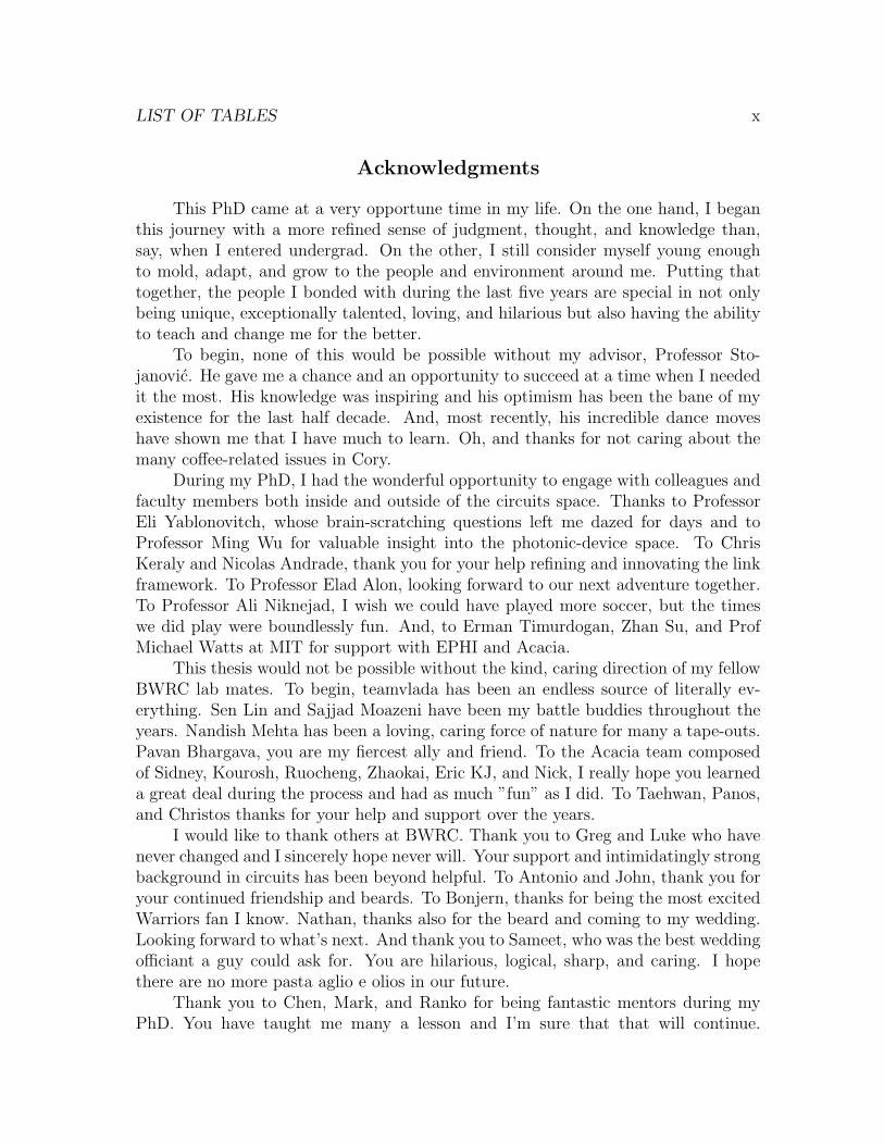
A photodetector (or photodiode) is a device which converts the incoming lightinto electrical current which may be decoded via the receiver circuitry. An examplephotodetector layout is shown in Figure 2.2.
The incoming waveguide provides the optical input to the photdetector. Basedon the absorption properties of the detector, which are heavily dependent on the char-acteristics of the material composition, the detector generates a current proportionalto the magnitude of the input optical signal. Indeed, because of the broad-band na-ture of the photodetector, a microring is generally appended before the photodiodeitself to allow for wavelength selectivity.
Once again, from the context of an optical link system, particular specificationsat the photodetector device level become critical in influencing the overall energy perbit. Namely, the three biggest contributors in performance are the optical bandwidth,responsivity, and added capacitance. The optical bandwidth of the photodetector,
CHAPTER 2. BACKGROUND 6
Figure 2.2: The photodetector is responsible for generating an output current depen-dent on the input optical power.
or equivalently the Full Width Half Max (FWHM) of the pulse response for a linearphotodiode, is a byproduct of transit time limitations of the material itself. Anydegradations in generating carriers slows down rise/fall times of the incoming bitstream. The responsivity of the photodiode dictates how efficiently the device is ableto generate electron/hole pairs. Lastly, the capacitance of the photodiode influencesthe electrical bandwidth. Contingent on the resistance seen by the photodiode, theresulting R-C time constant needs to be sufficiently high to not cause signal powerroll-off. All of these specs, again combined with the CMOS properties of the receiver,influence the best-case performance of the link. Moreover, co-designing the varioussub-components of the link (both CMOS and photonic) are critical in attaining theglobal optima.
2.1.2 Optical Communication Links
Putting together the sub-components detailed above along with an electronicbackbone to encode, decode, and control the optics, a full optical link, shown inFigure 2.3 can be designed.
Figure 2.3 shows a bank of microring modulators on the transmit side and asimilar bank on the receive side which drops the light onto the respective photodiodes.Notice also the presence of serializers and deserializers which aim to provide a lowspeed communication means to the rest of the digital backend. Additionally, thepresence of thermal tuners on both sides allow the ring to maintain resonance lock

CHAPTER 2. BACKGROUND 7
Figure 2.3: A WDM link composed of many transmit and receive side rings is anattractive solution which allows high bandwidth density.
despite thermal aggressors surrounding the system. In general, a separate drop portalongside the microring picks up fractions of the incoming light to allow for passive,background monitoring and tuning. Later in this work, during the design process forthe Acacia system, a new type of thermal tuner will be introduced which does notrely on this added drop port. Rather, careful monitoring of the data sequence itselfenables one to extract the approriate resonance information to ensure locking.
2.1.3 Circuit Design Challenges and Methodology
The best case energy per bit performance of an optical link is dependent on amultitude of factors. Parameters like data rate, technology, circuit topology, para-sitics, etc. all influence the behavior and design of the system. Indeed, trade-offsbetween the devices, the technology, and system architecture all motivate the utiliza-tion of an all-encompassing photonic plus CMOS co-design. As will be the objectiveof later chapters, this precise co-design approach will be enforced in producing designswith optimal performance.
However, as is painfully evident to all high speed circuit designers, layout para-sitics, matching, and other layout-specific design attributes greatly influence perfor-mance and functionality. As such, a design and layout engine or framework with theobjective of simplifying the design and execution of these blocks is paramount. Aswill be detailed in Section 2.3, this framework combined with the co-design mantradetailed above, high speed, high performance optical link systems may be realizedwith ease.
2.2 Silicon Photonic Integration Platforms
The integration platform with which the photonic and CMOS components in-tertwine is a key parameter which influencing the overall performance. Namely, the

CHAPTER 2. BACKGROUND 8
parasitic characteristics associated with the interconnect may easily become a bot-tleneck in performance. This section will detail the two main platforms used in thisdissertation. Both of these platforms are heterogenously integrated platforms, mean-ing that the CMOS and photonics are designed independently on separate wafers.Shortly thereafter, they are attached to one another either using through-oxide vias(TOVs)and C4 (µBumps).
2.2.1 3D Integration Using Thru-Oxide Vias
The first wafer-scale 3D integration using TOVs was developed by the SUNYCollege of Nanoscale Sciences (CNSE).
Figure 2.4: A cross section and top view of the TOV are shown.
The TOV, shown in Figure 2.4, connects the top metal layer of the CMOS waferwith that of the photonics. The process relies on firstly flipping the CMOS wafer,etching away the substrate to further reduce capacitance, and then punching TOVs toallow connectivity. With this approach, approximately 3fF of capacitance per TOVwas observed. Indeed, this technique was utilized for demonstrating a full end-to-endlink and will be detailed in a later chapter.
2.2.2 3D Integration Using Flip Chip µBumps
Using µBumps is another popular technique to allow integration of the CMOSand photonics. In this technique, small, conductive balls are first placed on the toppassivation opening of the wafer. The other wafer is then flipped and aligned onto thefirst. Once the alignment is correct, the balls are melted and collapsed to effectively

CHAPTER 2. BACKGROUND 9
solder the connection between the two wafers. Using this technique, past work hasdemonstrated 20-50fF of capacitance per bump. However, their high yield and processdependence proves this techique promising.
2.3 Analog Circuit Design Challenges and Automa-
tion
As was detailed beforehand, analog and mixed signal design motivates the ne-cessity of an alternative means of design. The Berkeley Analog Generator (BAG) isa framework that captures the methodology of the designer within the confines ofa new framework that provides many useful features. More specifically, this frame-work allows not only for layout parameterization (which produces push-button designrule check clean and layout-versus-schematic clean designs), but rapid iteration ondesigns. Function calls enable generation of new designs, calls to simulators, parsingthe simulator output results, and iterating quickly based on the feedback. BAG wasutilized in the Acacia system for all analog and mixed signal sub-blocks.
2.3.1 BAG Architecture and Flow
2.3.1.1 Overview
An example BAG-based design flow which an engineer may undertake is shownin Figure 2.5.
Figure 2.5: The design flow of a new block within the BAG framework is shown.
Here, the objective is to design a DLL within the BAG framework. Due to therapid iteration abilities of the framework, along with the reusability of past designs,the designer begins by checking the existing work for a similar script to run. Addi-tionally, due to the parameterizable attributes of BAG-generated layouts, a multitude

CHAPTER 2. BACKGROUND 10
of DLLs may be generated with a single design script, all at the push of a button.This allows for rapid reusability, contingent on the generator writer’s scope for us-age. Should the original generator not meet the needs of this specific architecture,the designer may choose to write his or her own generator, specific to the method-ology employed by said designer. Lastly, iteration is highly possible based on theoutput of characterization scripts and simulations. Verification of specifications canalso be done within the framework. This feedback-based design flow information issummarized in Figure 2.6.
Figure 2.6: The design flow with feedback from the output of simulations enablesrapid iteration. [4]
2.3.1.2 Design Example: StrongArm Sense Amplifier Generator
To further understand the design usage of the BAG framework, an examplegenerator for a simple sub-block is outlined below. In this case, a StrongArm senseamplifier is chosen as the block of interest.
The StrongArm sense amp, shown in Figure 2.7, functions as a rudimentaryanalog-to-digital converter. The block takes as input two small analog voltages andgenerates rail-to-rail swing outputs. It does this by relying on the current dischargepath of the input pair, followed by the cross-coupled action of the inverters.
Figure 2.7 not only shows the schematic, but also the example transient waveformof the outputs during the evaluation phase. Notice that the evaulation phase iscomposed of the initial linear (or integration) phase of the StrongArm followed by

CHAPTER 2. BACKGROUND 11
Figure 2.7: The schematic, transient, and example floorplan of the StrongArm isshown.
the evaluation phase wherein the outputs cross-couple to opposite railed values. Thisis then proceeded by the reset phase, wherein both outputs take a VDD value.
An important first step when undertaking designing a block within the BAGframework is to draw a sample floorplan of the block (this presumes that the topologyis “fixed” or needs little maneuverability).This floorplan not only shows the positionsof the various transistors and important signal wires, but also shows the directionof growth for the various transistors. The drawing of the important signal wires aidin identifying critical layout-dependent characteristics, such as presuming differentialmatching or minimizing trace lengths. The floorplan drawing aids the designer inproperly coding up routings without the mental hassle of remembering all growthconditions and layout design constraints. The floorplan is then coded within thePython-based framework as a layout generator. The code itself follows a “boiler-plate” template, beginning with importing the parameter values, specifying the totalwidth per row (within the framework, each horizontal row of transistors assumes afixed FET width but can have variable number of fingers), drawing the basic templatelayout, instantiating the transistors themselves, creating the wire connections, andfinally adding pins and fillers.
The schematic generator is also written by the designer, but is substantiallyeasier to implement than the layout generator script. A simple template schematicfollowed by appropriately updating the parameters is sufficient to create a generatorwhich outputs parameter-specific schematics. The layout generator script, combinedwith the schematic generator, produce unique schematic and layout instances depen-dent on an input list of parameters, such as FET widths, and number of fingers. A

CHAPTER 2. BACKGROUND 12
sample output of the generators is shown in Figure 2.8.
Figure 2.8: The output of the schematic and layout generators produce DRC andLVS clean instances of the StrongArm.
Indeed, with this layout and schematic generator, various instances of the Stron-gArm sense amplifier can be designed with the push and execution of the code. Bysimply modifying the dimensions of the transistors, instances such as those in Figure2.9 can very easily be generated and verified. Notice that because the generator waswritten with sizing parameters incorporated within the layout, any permutation oftransistor widths would easily yield DRC and LVS clean layout designs.
Figure 2.9: The framework allows for push-button instantiation and verification togenerate quick, correct instances.
To further ensure that a layout and schematic are behaving properly when sim-

CHAPTER 2. BACKGROUND 13
ulated, any particular instance can be pushed through the “entirety” of the flow,enabling rapid layout and schematic generation, verification, and post-PEX simula-tion to ensure the design specifications are met. This is highlighted in Figure 2.10.Input parameters, both within the layout and also within the simulation environment,can be modified and the design can proceed through the flow. The log shows the gen-eration of the layout and schematic, run LVS, run PEX simulations, and analyze theresulting outputs. The waveforms are processed and shown in the right side of Figure2.10.
Figure 2.10: Pushing an instance through a full design flow is simple within thiscodified environment.
2.4 Conclusion
In this chapter, we introduced the foundational blocks of both silicon photonicsand analog automation. In providing this introduction, the reader should take carefulnote on the power of growing vast systems which rely on the marriage of these un-derlying foundations. Notably, understanding the device and block level parametersthat influence macro-specifications at the system level is a powerful step in design-ing high performance optical links. Moreover, realizing that operating at these highspeed-high performance corners rely heavily on layout parameters is the key to mo-tivating the need for analog automation. With these two in mind, the rest of this

CHAPTER 2. BACKGROUND 14
thesis aims to operate at the intersection of these foundations – one that focuses onmulti-hierarchical fundamental theory and the other which focuses on executing andoptimizing beginning with the “optimized” circuits and ending with physical design.

15
Chapter 3
End-to-End Optical Link DesignMethodology
3.1 Introduction
Optical interconnects, after having completely replaced electrical interconnectsfor long haul communication, are forecast to continue their expansion to shorter andshorter links, eventually bringing data directly to the processing chips, and evenpotentially replacing some of the longer interconnects on the chip itself [5]. Thisis due to several key aspects of optical interconnects: their potential for extremelyhigh bandwidth, distance insensitivity of optical channel loss when compared withelectrical, and better optical components and technology. Nevertheless, as illustratedin Fig. 3.1, in a world where energy dissipation from computing units is becomingincreasingly important, optical links must still prove that they can offer a more energyefficient communication means than electrical links for shorter distances.
Commonly cited objectives for chip to chip links range in the ∼ 100fJ per bit,and drop to ∼ 10fJ per bit when considering on-chip interconnects [6]. These energyrequirements, when combined with the extremely high bandwidths needed, still pose anumber of challenges for optical links. The emergence of Silicon Photonics is offeringnew possibilities and prospects in this regard by enabling seamless integration ofphotonics and electronics on a single platform, thereby increasing energy efficiency.The purpose of this work is to model these links and optimize them in order to explorewhat limits can be reached in terms of energy efficiency and how these limits dependon the specific technology available.
Prior literature in this space has made strides in accurately modeling particularaspects of the link data path, namely the front-ends and the systems-level energybreakdowns ( [7–9]). However, a proper marriage between ”analog”-dominated and”digital”-dominated constraints has yet to be demonstrated. More specifically, inthe context of optical receiver design, specifications on the sensitivity and power

CHAPTER 3. END-TO-END OPTICAL LINK DESIGN METHODOLOGY 16
109
1010
1011
10−15
10−14
10−13
10−12
10−11
10−10
Data Rate (Hz)
En
erg
y p
er
bit (
J/b
)
on chip
chip to chip
Figure 3.1: Demonstrated Optical Link Efficiencies [6-15], Against Objectives From[6]. Further information at linksurvey.eecs.berkeley.edu.
Figure 3.2: Optical Link System Overview
of the signal are contingent on the interaction of the front-end and the follow-onsamplers that ultimately convert the analog signal into a digital bit, to set the overallenergy, bandwidth, gain and noise properties. Linking all of these relevant interactionstogether, this work shows the behavior of the full optical link under different regimesof operation from the context of energy-efficiency and noise.
In this chapter, we will introduce and analyze the optical modeling framework,beginning with a high-level link picture and slowly delving down into the various sub-components. The theory and “interface” between these blocks will also be studied.Once this foundation has be layed out, the focus will shift to the link-level, wheremacro-parameters will be derived and initial trade-offs will be studied. Lastly, usingthe framework, performance projections will be made which, in turn, gives insightinto the direction of possible fabrication improvements in the future.

CHAPTER 3. END-TO-END OPTICAL LINK DESIGN METHODOLOGY 17
3.2 Optical Link Modeling
We consider a very general model for the optical link, which enables us to performoptimizations on its topology and estimate the optimal energy per bit which can beachieved at particular data rates given the technology constraints. The parameterizedmodel topology is depicted in Fig. 3.2 and is detailed as such: the receiver element isconstructed with a transimpedance front end followed by N amplifications stages andterminated with a sampling unit composed of M individual samplers. The number ofamplification stages N, the size of each stage, the number of sampling units M and thesizing of its transistors constitute optimization variables. There is of course a varietyof other receiver topologies or variations on the one suggested. The framework wedescribe next will be readily extendable to these topologies.
The energy consumed in the receiver can be computed from the bias currentsand circuit capacitances, and its sensitivity is determined by two constraints: a noiseconstraint, and a system output voltage constraint. Finally, the energy consumed bythe transmitter can be calculated starting from the receiver sensitivity requirement,and back-propagating that through the data path losses to the transmitter. The totalenergy is the sum of the receiver and transmitter energy, which is minimized withrespect to the optimization variables at hand.
3.2.1 High-Level Receiver Abstraction
The receiver is modeled as illustrated in Fig. 3.2. The front end consists of atransimpedance amplifier (TIA) that converts the input photocurrent to an outputvoltage signal, and is followed by N chained gain stages forming a voltage amplifier(VA) to further amplify the signal. All these amplifiers are considered to be first orderstages (except for the TIA which has two poles: one from the photodiode capacitanceand feedback resistor, and one from the input capacitance of the VA ). The chaining ofsuch stages causes the overall bandwidth to degrade. The bandwidth Bchain resultantfrom N first order stages of bandwidth fS is [19]:
Bchain ∼ fS0.9√N + 1
(3.1)
We set the target end-to-end bandwidth to 0.7×fdata, where fdata is the Nyquistrate of the input data stream. This implies that the bandwidth fS of each stage mustbe
fS > 0.7fdata
√(N + 2) + 1
0.9(3.2)
in order to satisfy this constraint. The factor of 2 comes as a result of the twopoles imposed by the TIA.

CHAPTER 3. END-TO-END OPTICAL LINK DESIGN METHODOLOGY 18
3.2.2 Gain-Bandwidth product
While the unity current gain-bandwidth of a technology is fT , the actual gainbandwidth that is achieved in an individual gain stage that is loaded by its replica willbe lower due to various parasitics and non idealities. Additionally, different gain stagetopologies will yield different GBWs. For example, inductive peaking is a popularway of enhancing the bandwidth and will yield a higher GBW than simple resistively-loaded stages. Therefore we use a parameter α which describes what fraction of fTis achieved by each individual gain stage. The GBW of a replica-loaded stage istherefore fa = αfT .
3.2.3 Voltage Amplifiers
Here, we introduce the analysis of the follow-on voltage amplifiers, which helpslay the foundation for the analysis of the transimpedance amplifier stage. Every stagein the voltage amplifier is defined by input transistor gate width Wgate,i (where ”i”denotes its position in the amplifier chain), which then also defines its transconduc-tance gm,i, gate capacitance Cox,i and bias current Id,i. To simplify the problem, weassume that gm, Cox, and Id are simply proportional to Wgate, which implies thatthe biasing for each transistor is relatively similar– a reasonable assumption to firstorder. The GBW of each stage depends on the capacitance seen at the output, and inthe case of simple resistively loaded stages, we have GBWi = gm,i/(Cout,i + Cin,i+1).We define β = Cout/Cin as the ratio of output to input capacitance of a gain stage.Similar to α, β is dependent on the stage topology.
In the model, two factors are used to characterize the individual gain stages:α = fa
fT, the ratio of the gain bandwidth to fT of a replica loaded stage, and β = Cout
Cin,
the ratio of input to output capacitance. Here we calculate α and β for simple gmRL
topology and cascode stages for the 65nm platform used.
3.2.3.1 α-factor Derivation
For a simple gmRL topology we have
Cin = Cox + ACgd (3.3)
where the second term accounts for the Miller Effect, and Cout = Cgd + Cds. For acascode stage, we have
Cin = Cox + Cgd (3.4)
Notice that the CGD seen by the input does not see the Miller effect due to theintermediary FET between the input FET and the output node.
Given that Cox = 0.5fF/µm, Cgd = 0.2fF/µm, Cgs = 0.27fF/µm, we haveα = 0.36 for a standard gmRL stage and α = 0.4 for a cascode stage.

CHAPTER 3. END-TO-END OPTICAL LINK DESIGN METHODOLOGY 19
3.2.3.2 β-factor Derivation
With the expressions given above, it is easy to show that β = 0.29 for gmRl
stages and β = 0.4 for cascode stages.To summarize,
fa =gm
(1 + β)Cin
(3.5)
and we can derive the GBW of every stage as:
GBWi =gm,i
Cout,i + Cin,i+1
= fa1 + β
β +Wgate,i+1
Wgate,i
(3.6)
As mentioned earlier, each gain stage must also have a 3-dB bandwidth of fS,so that the DC gain of stage i in the linear amplifier is:
GDC,i =fafS
1 + β
β +Wgate,i+1
Wgate,i
(3.7)
The maximum gain is capped by the intrinsic gain of the devices gmr0. For thelast stage, the capacitance driven is the sampler’s input capacitance CSA. Finallythe power consumed by each stage is VDDIbias,i, where Ibias,i = gm,iVov, where Vovis the stage overdrive voltage, which is considered to be the same for every stage.The motivation for the constant overdrive voltage stems from insight gained whileexecuting the optimization framework. Namely, adding Vov as an optimization pa-rameter yielded little performance improvement over holding it constant, while addinga significant time overhead in terms of optimization convergence.
3.2.4 Transimpedance Amplifier
The transimpedance amplifier (TIA) is composed of a gain stage similar to thosein the VA, with a feedback resistor chosen to meet the bandwidth requirement perstage (fS). The open loop gain is calculated similar to the VA stage gain. Thefeedback resistor is therefore set to:
RFB =GDC,TIA
2πfS(CPD + Cin,T IA)(3.8)
where CPD is the photo-detector parasitic capacitance including the interconnectbetween the photo-detector and the TIA, and Cin,T IA is the TIA input capacitance.The two poles resulting from the TIA designed in this fashion are not real, and the

CHAPTER 3. END-TO-END OPTICAL LINK DESIGN METHODOLOGY 20
damping factor is ζ = 12
2+GDC,TIA1+GDC,TIA
bounded as 0.5 < ζ < 1, implying the bandwidth
is marginally greater than if the poles were real. This means that (3.2) slightlyoverestimates the required bandwidth per stage. To first order this is an acceptableapproximation.
The total transimpedance gain of the front end is therefore
Rtot =RFB GDC,TIA
1 +GDC,TIA
N∏i=1
GDC,i (3.9)
Figure 3.3: StrongArm Sampler Schematic
3.2.5 Sampler Model in Receiver
The role of the sampler is to bring the signal coming out of the amplifier to logiclevels so that the digital circuit can effectively process it at the output. The modelingdescribed here enables the efficient optimization of transistor sizes in order to yieldoptimal sampler performance in terms of sensitivity and power consumption. Mostsamplers rely on a positive feedback latching mechanism, such as a cross coupledinverter pair in order to achieve exponential gain and recover digital levels from

CHAPTER 3. END-TO-END OPTICAL LINK DESIGN METHODOLOGY 21
extremely low signal voltages. The sampler analyzed here, and depicted in Fig. 3.3is known as the StrongArm, but the presented analysis and trends can be generalizedto a large family of sampler topologies, such as CML-based samplers or more exotictechniques such as double-tail sampling.
3.2.5.1 StrongArm Operating Principle
Before the sampler starts evaluating, the clock is down, and the nodes P,Q,X andY are brought up to VDD by the reset transistors driven by clock, φ. The evaluationstarts when the clock goes up, and is composed of two periods,: the sampling period,where in the nodes P,Q, X and Y discharge through M1, M2, M3, M4 and M7,building a differential voltage on nodes X and Y. The sampling period ends whenVX,Y reach VDD−Vth,P and the cross coupled inverters composed of M3, M4, M5 andM6 turn on. The regeneration then starts and the differential voltage on nodes X andY is amplified to logic level by the latch.
3.2.5.2 Sampling Period
The sampling phase can itself be divided into two separate phases. The first,during which only M1 and M2 are on, discharges nodes P and Q until they reachVDD − Vth,N . The common mode voltage VPQ behaves as VDD − I1t
CPQwhere I1 =
gm1,2VCM is the current drawn by the common mode and lasts t1 =Vth,NCPQ
I1
The second phase starts when M3 and M5 are also on, therefore dischargingnodes X and Y. It ends when VXY = VDD − Vth,P . The common mode behaves ac-cording to
VXY = VDD −I1
CPQ + CXY
[(t− t1) + τ(exp(−t− t1τ
)− 1)] (3.10)
where τ =CXYCPQ
gm,3(CXY + CPQ)(3.11)
There is no closed form solution to determine when nodes XY reach VDD−Vth,P ,but if τ is small compared to Vth,P (CPQ +CXY )/I1, which is usually the case, the endtime of the second sampling phase may be approximated as
t2 ∼Vth,P (CPQ + CXY )
I1
+ τ + t1 (3.12)

CHAPTER 3. END-TO-END OPTICAL LINK DESIGN METHODOLOGY 22
The differential mode, during the second phase, can be shown [20] to follow theequation:
d∆VXY
dt=gm3,4
CXY
(1− CXY
CPQ
)∆VXY − gm3,4∆It
CPQCXY
(3.13)
∆VXY (t) =
∫ [gm3,4
CXY
(1− CXY
CPQ
)∆VXY − gm3,4∆It
CPQCXY
]dt (3.14)
∆VXY (t) =gm,1
CXY − CPQ
(t− t1 + τ∆(1− exp(t− t1τ∆
)) (3.15)
τ∆ =gm,3
CXY
(1− CXY
CPQ
) (3.16)
Since CXY is usually greater than CPQ, τ∆ is usually negative, and there is no re-generation gain during the sampling period. The sampling gain can be approximatedas
G ∼ VthreshVCM − Vthresh
CPQ + CXY
CXY − CPQ
(3.17)
3.2.5.3 Regeneration Period
Once the top PMOS transistors turn on, the regeneration period starts. Theapproximation is made that only the cross-coupled inverter pairs are on, providingpositive feedback gain, with a time constant
τreg =gm,3 + gm,5
Cin,D2S + Cout,SA
(3.18)
3.2.5.4 StrongArm Model within Framework
The modeled sampling stage is made of M interleaved StrongArm samplers (alsoreferred to as Sense Amplifiers (SA)), that evaluate the bits sequentially. This meanseach individual StrongArm has a cycle M ×Tbit long. Half of this period is dedicatedto the resetting of the sampler, while the other half is dedicated to the integration andregeneration of the bit (minus the setup time of the follow-on flip-flop TD2S) so thatthe actual time the sampler is evaluating is TSA, given in (3.21). The schematic of anindividual sampler is depicted in Fig. 3.3 and sample transient waveforms are shownin Fig. 3.4. The blue and red lines show the complementary outputs of the StrongArmsampler (nodes X and Y in Fig. 3.3). The integration period lasts while the inputpair discharges nodes P,Q,X and Y until nodes X and Y reach VDD − Vth,P whichdictate when the cross coupled pair turns on and the regeneration period starts [20]

CHAPTER 3. END-TO-END OPTICAL LINK DESIGN METHODOLOGY 23
(Vth,P is the threshold voltage of the PMOS). Fig. 3.4 shows a StrongArm’s transientcharacteristics with the three main regimes of operation highlighted. The regenerationgain is generated by a cross coupled pair forming a latch, is exponential with time,and brings the output signal to logic levels.
Figure 3.4: Sampler Timing Evaluation Breakdown
The optimization variables available are the common mode voltages at the input,the gate widths of the input transistors, and the gate widths for the cross coupledpair transistors. These define the length of the integration period (which must stayunder Tbit in order to avoid intersymbol interference), the integration gain, and theregeneration gain. The size of the tail transistor, M7, is not considered to be anoptimization parameter and is sized to be at least 2x larger than the input pair, M1
and M2, and therefore not current-limiting the signal path.The sampler then drives a dynamic to static (D2S) converter stage which we
simply characterize as a load capacitance to the sampler, Cin,D2S [21]. The D2Srequires a fixed amount of time TD2S ∼ 2
fTto latch, which is taken out of the total
evaluation time. Approximations are nevertheless given here:

CHAPTER 3. END-TO-END OPTICAL LINK DESIGN METHODOLOGY 24
Tint ∼VTH(2CPQ + CXY )
gm,1(VCM − VTH)(3.19)
Gint ∼VTH
VCM − VTH
CPQ + CXY
CXY − CPQ
(3.20)
TSA = M/2× Tbit − TD2S (3.21)
GSA ∼ Gintexp(TSA − Tint
τreg) (3.22)
τreg =gm,3 + gm,5
Cin,D2S + Cout,SA
; (3.23)
where VTH is the absolute value of the threshold voltages and GSA is the finalsampler gain. Finally the input capacitance of the SA seen by the front end is givenby M ×Cox,SA. The fanout M is detrimental to the gain of the front end, and, as willbe shown, can be amortized by using switches that connect only one sampler at atime to the output of the VA. In this case, the input capacitance seen by the front endis approximately Cox,SA neglecting wire capacitance and junction capacitance effectsof the sampling switches and the RC time associated with them. This assumptionholds true for reasonable number of samplers:
M <fTfdata
Cox
Cgd
(3.24)
Indeed the size of the transistor serving as a switch can be made substantially smallerthan the input cap of the SA, by a factor ∼ fT
fdatato minimize it’s effect on the
circuit bandwidth, and the only capacitance it presents to the circuit is it’s gate-drain capacitance, justifying (3.24).
The energy consumed by the sampler comes from the charging and dischargingof all it’s capacitances at each cycle, as well as the dynamic power burned by thecross coupled inverter during the latching process:
Esamp = ECap + Elatch (3.25)
ECap = CSAV2DD (3.26)
Elatch ∼ (gm,3 + gm,5)(VDD
2− VTH)VDD(TSA − Tint) (3.27)
where CSA comprises all the capacitances that will have to be charged to VDD
during the reset period.

CHAPTER 3. END-TO-END OPTICAL LINK DESIGN METHODOLOGY 25
3.3 Macro-Parameter Derivations
3.3.1 Sensitivity calculation
The sensitivity calculated for the receiver can be separated into two parts: thesampler swing requirement, and the circuit noise requirement. The final sensitivityis the sum of the two.
3.3.1.1 Swing Based Sensitivity Requirement
The swing requirement represents the signal needed to ensure that the differentialvoltage at the output of the sampler reaches VDD by the appropriate time, and iscalculated from the sampler gain, the TIA gain and the VA gain:
Ireq,swing = 2VDD
RtotGSA
(3.28)
The factor of 2 comes from the fact that the signal is only half the actual photon cur-rent magnitude for an optical ONE (during a ZERO, the photon current is assumedto be nil). Slight changes must be made if the modulation extinction ratio of thetransmitter is finite, but the general framework is the same.
3.3.1.2 Noise Based Sensitivity Requirement
The noise requirement necessitates the calculation of the input referred noisegenerated by the amplification circuit. These include the feedback resistor thermalnoise, the Johnson noise from the TIA’s transistors, and the transistor noise fromthe follow-on transistors as well as the noise from the samplers. The TIA transistorand resistor noises are calculated using Personick’s method, with all the Personickintegrals set to unity [22], while the follow-on stages are estimated using approxi-mations consistent with literature [23]. The photon shot noise (or PD shot noise)is neglected as it is always much lower than the circuit noise sources for incoherentdetection systems (roughly one order of magnitude). Indeed for a BER of 10−12, thelimit that would be imposed by photon shot noise is 27 photons per bit during a ONE(also known as the quantum limit), which is a current of 44 nano-Amps at 10 Gbps.Naturally when the other noise sources impose a higher photon current, the photonshot noise’s absolute value also goes up, but it will necessarily be smaller than theother noise sources.

CHAPTER 3. END-TO-END OPTICAL LINK DESIGN METHODOLOGY 26
I2noise,in,Rfb
=4kbθ
TbitRfb
(3.29)
I2noise,in,T IA =
16π2kbθγ(CPD + Cin,T IA)2
gm,TIAT 3bit
(3.30)
I2noise,i =
4kbθγ
gm,i[TbitRfb
∏GDC,j]2
(3.31)
V 2noise,SA =
8kbθγ
t2gm1
+8kbθγgm,3
t12g2m1
+2kbθ
Cout,SAG2sample
(3.32)
Here, kb is the Boltzmann Constant and θ is 273 Kelvin. The sampler voltagenoise is approximated using the methodology presented in [24].
Finally the sensitivity is calculated using a current SNR of 14 in order to achievea bit error rate of 10−12. Please note that this is for current magnitude SNR and notpower SNR.
Ireq,noise = SNR Inoise,input (3.33)
The total photon current requirement at the input of the photodiode is the sumof the swing current requirement and the noise current requirement:
Ireq,input = Ireq,noise + Ireq,swing (3.34)
3.3.2 Energy per bit
The total energy per bit that is consumed by the link is the sum of the energyburned in the transmitter and the receiver
Ebit = ERX + ETX (3.35)
ERX = TbitVDD
∑Ibias + Esamp (3.36)
ETX = TbitVTX(Ireq,noise + Ireq,swing) + Emod (3.37)
ERX includes the power burned in the amplification stages as well as the energyconsumed by the samplers. ETX includes laser energy and modulator energy Emod,where VTX represents the energy cost of transmitted photons that represent a bit

CHAPTER 3. END-TO-END OPTICAL LINK DESIGN METHODOLOGY 27
successfully detected at the receiver. It encompasses all the efficiencies, η, encoun-tered from the generation of photons to their absorption into useful photocurrent inthe receiver photodiode, such as the laser wall plug efficiency, coupler inefficiencies,waveguide losses, modulator loss, photodiode quantum efficiency, etc.
VTX =hν
q
1
η(3.38)
η =∏
ηsystem (3.39)

CHAPTER 3. END-TO-END OPTICAL LINK DESIGN METHODOLOGY 28
Tab
le3.
1:M
odel
inputs
and
opti
miz
atio
nva
riab
les
Model
inputs
Var
iable
des
crip
tion
65nm
het
erog
eneo
us
inte
grat
ion
f TT
echnol
ogy
unit
curr
ent
gain
freq
uen
cy15
0G
Hz
CPD
Phot
odio
de
capac
itan
ce20
fFf d
ata
Dat
arat
e1
Gbps
to50
Gbps
αF
ract
ion
off T
for
self
load
edst
age
GB
W0.
29(s
tandar
dg mR
Lst
ages
)0.
4(c
asco
de
stag
es)
βF
ract
ion
ofin
put
toou
tput
cap
ofa
gain
stag
e0.
67C
out,D
2S
D2S
input
capac
itan
ce3
fFt D
2S
D2S
latc
hin
gti
me
requir
emen
t25
ps
VDD
Supply
volt
age
1.6V
VTX
Vol
tage
cost
ofphot
ons
580
V(g
mr 0
) max
Max
imum
volt
age
gain
per
stag
e4
Vov
Ove
rdri
vevo
ltag
e0.
3V
γnoi
sefa
ctor
2/3
Emod
Modula
tor
ener
gyp
erbit
0O
pti
miz
ati
on
vari
able
sB
ou
nd
sN
Num
ber
ofam
plifica
tion
stag
es0
to4
MN
um
ber
ofsa
mple
rs(M
-DR
)1
to64
,in
pow
ers
of2
Wgate,T
IA
Input
tran
sist
orga
tew
idth
for
the
TIA
>15
0nm
Wgate,1,...,N
Input
tran
sist
orga
tew
idth
for
each
stag
e>
150n
mW
gate,in,SA
Input
tran
sist
orga
tew
idth
for
sam
ple
r>
150n
mW
gate,C
C,SA
Tra
nsi
stor
gate
wid
thfo
rcr
oss
couple
dpai
r>
150n
mVCM
Com
mon
mode
volt
age
atSA
input
0.8V<...<
1.4V
=VDD/2
ifN
=0
CHAPTER 3. END-TO-END OPTICAL LINK DESIGN METHODOLOGY 29
3.3.3 Model inputs and optimization variables
The model described enables us to rapidly predict the performance of a givenoptical receiver characterized by the number of amplification and sampling stages,the technology available, and the size of the transistors involved. These differentparameters can therefore also be optimized in order to reach minimal total link energy.The optimization variables and model parameters are described in Table 3.1, and theoptimized links are presented in Figs. 4.1, 4.2 and Table 3.3.
3.3.4 Model purpose and limitations
The goal of the model is to accurately encompass all the most important effectsand limits that fundamentally constrain the performance of an optical link. Natu-rally, no model can include all practical limitations, such as systematic and randomtransistor mismatches, kickback, jitter, layout imperfections, etc. In particular, tran-sistor offset and mismatch can be of significant importance and its effects have beenextensively studied [25]. However, through calibration techniques, which indeed adddesign complexity, the effects of mismatch can be corrected while still adding a min-imal power penalty. Additionally, exotic amplification schemes such as higher orderstages, or multiple interleaving schemes are not included. While these considerationsare important in practical circuit design, we believe that our modeling approach isreadily extendable to include these considerations. The presented model will how-ever allow us to derive some general conclusions about critical link trade-offs. Itis also precise-enough to provide optimal transistor sizing and accurate sensitivitypredictions leading to functional circuits as those shown in Section IV.
3.4 Sensitivity and energy limits
While the model enables us to choose optimal transistor sizings and achieveoptimal system link efficiencies, it does not immediately provide us with a deep un-derstanding of the different limits experienced by such a system. In this section wederive these limits. As shown earlier, it is possible to alleviate the swing requirementby using an appropriate amount of interleaved samplers. In a similar way, if a trackand hold method is used as in Section 4.3.5 to negate the effect of interleaving fanout,we can make sure the dominant noise source comes from the very front end. We willtherefore focus on the limits imposed by noise in the TIA/VA front end.
3.4.1 Front end noise limit
The noise in the front end is dominated by the first amplification stage, whichis the TIA in this case. The two major sources of noise have been given in (3.29)

CHAPTER 3. END-TO-END OPTICAL LINK DESIGN METHODOLOGY 30
fdata+
=
Transfer func+ons classic with CTLE
TIA
Following amplifier
Full front end
Figure 3.5: Ideal Transfer Function of A System with Equalization
and (3.30), and their input referred noise current is given in (3.40) and (3.41). Theydepend on the input capacitance Cin,T IA of the transimpendance amplifier (though thefeedback resistor noise does not explicitly depend on it, the bandwidth requirementsets it’s value, so there is an implicit dependence), but they have lower limits, whichare given by
I2n,R = (qfdata)
28πCPD + Cin,T IA
6.4aF
fTIA
fdata
1
gmr0(3.40)
I2n,amp = (qfdata)
28π(CPD + Cin,T IA)2
6.4aF × Cin,T IA
fdatafT
γ
α(1 + β)(3.41)
Where fTIA is the bandwidth of the TIA, and 6.4aF = q/Vth where Vth is thethermal noise voltage. When both terms are present, the optimal Cin,T IA is somewherebetween 0 and CPD.The energy used in the laser to overcome the resistance noise is

CHAPTER 3. END-TO-END OPTICAL LINK DESIGN METHODOLOGY 31
constant with datarate if the bandwidth of the TIA scales linearly with the datarate,whereas the energy needed to overcome the transistor noise increases with datarate.Thus at lower datarates, the resistance term is likely to dominate. For the 5Gb/s casewhen using the parameters of table 3.1, we can calculate that the energy burned inthe laser to compensate for this noise is ETX = VTX SNR IR,min/fdata = 152fJ/bit,which is close to the energy predicted by the model (∼ 200fJ/bit). Naturally, sincethe model also optimizes for receiver energy, it is expected that it is not entirelyoptimized for feedback resistor noise.
Nevertheless, the feedback resistor noise can be overcome to some extent byincreasing the value of the feedback resistor, and compensating for the bandwidthdegradation by including equalization such as a CTLE stage, as we show in theexample circuit of Fig. 4.4. The total front end bandwidth is not enhanced in anyway since the TIA and the CTLE stage compensate each other, as illustrated in Fig.3.5, but this enables the use of a higher resistor value and therefore translates tosmaller input referred noise. In (3.40), this is illustrated by the fact that fTIA isreduced, therefore reducing the input referred noise. In this way, it appears that thetransistor noise is somewhat more fundamental than the feedback resistor noise.
3.4.2 Limits at high data rates
At high data rates, the input referred noise contributed from the transistors ishigh enough that laser energy required to overcome it will be the dominant source ofpower consumption. In this case the optimal receiver will be optimized purely for noiseand not its own power consumption, since it will be negligible. We can easily showfrom (3.41) that the optimal sizing for the input transistors will be Cin,T IA = CPD.This yields the transistor noise limit, which, expressed in terms of photons per bit fora ONE is:
nph,min = SNR
√32π
CPD
6.4aF
fdatafT
γ
α(1 + β)(3.42)
Naturally if this value comes close to the the quantum limit of 27 photons per bit fora ONE, the photon shot noise will start to take over.
3.4.3 Limits at low datarates
At lower data rates, the power will not necessarily be dominated by the laserpower. If we consider only the noise from the TIA transistors and the power con-sumption of the TIA and the laser, the energy per bit consumption of the link is:

CHAPTER 3. END-TO-END OPTICAL LINK DESIGN METHODOLOGY 32
Ebit = SNR VTXIn,ampTbit + ITIAVDDTbit (3.43)
= SNR VTXq
√8π
(CPD + Cin,T IA)2
6.4aF × Cin,T IA
fdatafT
γ
α(1 + β)
+ Cin,T IA(1 + β)2πfaVovVDDTbit (3.44)
In this case, there is an optimal size for Cin,T IA. The lower the data rate, thesmaller the input capacitance of the TIA will be in order to minimize power consump-tion for that stage. To obtain an analytic expression, we assume that Cin,T IA << CPD,which leads to:
Ebit,opt = 3[πSNR VTXCPD]2/3[VDDVovγkBθ]1/3 (3.45)
Concluding from (3.45), the optimal energy per bit in this case does not dependon the datarate or the speed of the transistors fT when the link energy is not domi-nated by the laser power.
3.4.4 E/b power laws
The limit between these two regimes is when we can no longer use the approxi-mation Cin,T IA << CPD which is only valid when
4(SNR VTX
2VDDV ∗ )2/3(qVthγ
CPD
)1/3 1
α(1 + β)<<
fTfdata
(3.46)
With the photonics platform which will be further elaborated in Chapter 4, thisleads to fT
fdata∼ 15 which clearly states why 25Gb/s is in the laser limited regime,
whereas 5Gb/s is in the full link limited regime. The power laws for optimal En-ergy/bit of these different regimes is summarized in Table 3.2.
3.5 Observations in Scaling and Technology
With performance limitations arising from both the quality of the CMOS andphotonic devices, this section aims to study the effects of an improved design platformwith respect to optimized energy per bit. Following the previous analytic analysis,here we utilize the model and optimization procedure described in section 3.2, andapply it to different hypothetical technology platforms. This enables the capture ofadditional effects such as sampler energy not described in section 3.4. In doing so,we hope to target key bottlenecks in performance and potential for improvements inthe next-generation of integration technologies.

CHAPTER 3. END-TO-END OPTICAL LINK DESIGN METHODOLOGY 33
Table 3.2: Minimum power laws for E/b limits dependence
Variable TX dominated regime TX and RX balanced regime
Regimes defined by (3.46)
CPD 1/2 2/3
VTX 1 2/3
fdata 1/2 0
ft -1/2 0
3.5.1 Improvements in Photonics and Interconnects
Parasitics such as coupler losses and photodiode capacitance dominate the plat-form described in Table 3.1 and limit the achievable energy efficiency. To studythe importance of the photonic performance, we replace the existing metrics forcoupler losses, modulator loss, laser efficiency and photodiode capacitance, CPD
from 3.5dB/coupler, 5dB/modulator, 10% laser effeiciecy and 20fF to 1dB/coupler,3dB/modulator, 30% laser and 3fF, respectively, implying VTX = 15V . In addi-tion, modulator efficiency as low as 1 fJ/bit have been demonstrated, justifying theiromission from this analysis [27].
The results of the analysis are shown in Fig. 3.6. As compared with the existingheterogeneous integration platform, using better photonics shows more than an order-of-magnitude improvement in link efficiency. Because the price to convert from thephotonic to electrical domain, VTX , is so cheap now, the optimized links at the variousdata rates are more receiver-performance limited, as expected intuitively.
3.5.2 Improvements in Photonics+CMOS
To push the boundary of integration technologies altogether, we now turn to thecase where the photonics and CMOS are both pushed to their bounds. In particular,we utilize the same best photonic specifications from before, but, now, scale the tech-nology node to reflect a theoretical fT of 1THz. The results of the study are shownin Fig. 3.6. For lower data rates, the performance improvement from scaling fT from150GHz to 1THz is observable but not drastic and stems mostly from the lower en-ergy consumption of the samplers themselves and not the front end amplifier or thelaser, as expected from the limits of section 3.4. For the 25G DDR case, however, theimprovement is almost an order of magnitude since the faster amplifiers can providegain at these speeds. Notice that the last column in this bar plot shows a 100G DDRreceiver, with a theoretical best end-to-end link efficiency of 20fJ/bit.
While the previous sections show the performance for given technologies, we can

CHAPTER 3. END-TO-END OPTICAL LINK DESIGN METHODOLOGY 34
reverse the exercise to deduce the necessary technology properties for a given linkefficiency. To achieve sub 1fJ/bit efficiency at 5Gbps and ft=1000 Thz, this wouldrequire CPD=200 aF, VDD=0.5 V, Vov=0.1 V and VTX=10 V. These small photodiodecapacitances would require such a small device that some sort of absorption enhance-ment would be necessary, such as a cavity or a metaloptic focusing scheme [28]. Atthis point the link energy itself is so small that effort must be redirected to the energyoverhead of peripheral blocks such as clock networks and bias generators.
The performance results for these higher data rates have another interestingtrend – as the CMOS platform performance improves, the energy consumption ofthe receiver is mostly limited by the sampler itself. Because we have assumed aStrongArm topology for the sampler for all data rates of operation, the minimumachievable E/b of this sampler is far greater than the rest of the link put together.This yields the conclusion that within the confines of a better platform where photonefficiency is so high, using a simple gain stage such as an inverter as the sampler ismore optimal than having a StrongArm or CML latch.

CHAPTER 3. END-TO-END OPTICAL LINK DESIGN METHODOLOGY 35
Tab
le3.
3:P
erfo
rman
ceC
ompar
ison
ofM
odel
-Pre
dic
ted
and
Sch
emat
ic-S
imula
ted
Opti
cal
Rec
eive
rs
Sp
ecifi
catio
n5G
bps
Sta
ndard
RX
5G
bps
CT
LE
RX
25G
bps
DD
R25G
bps
QD
R25G
bps
Sw
itchin
gQ
DR
Modele
dD
esig
ned
Modele
dD
esig
ned
Modele
dD
esig
ned
Modele
dD
esig
ned
Modele
dD
esig
ned
Tota
lFro
nt-
end
Gain
(Ω)
15500
20200
15500
15500
636
770
1055
760
1750
1840
Tota
lFro
nt-
end
BW
(GH
z)
3.5
3.4
3.5
3.4
17.5
18.8
17.5
20.5
17.5
17.8
Tota
lA
FE
E/b
(fJ/bit
)79
52
79
91
340
300
260
395
‘134
135
Tota
lSam
ple
rE
/b
(fJ/bit
)32
35
32
37
110
97
93
153
88
91
Tota
lR
XSensi
tivit
y(µA
)3.3
73.8
2.9
53.2
356
288.2
33.9
86.2
28
77.4
SA
Input
Com
mon
Mode
(mV
)500
500
500
530
850
840
850
810
850
950
SA
Min
imum
Sw
ing
(mV
)0.2
60.2
5210
165
1.6
41.5
11
RX
Sw
ing
Sensi
tivit
y(µA
)0.0
10.8
0.0
12.1
326
214
1.7
50.9
614σ
RX
Nois
eSensi
tivit
y(µA
)3.4
2.9
2.9
1.1
30.8
74.3
32.2
81.2
26.6
71.4
Lin
kR
XE
/b
(fJ/bit
)110
88
110
128
440
400
225
550
221
227
Lin
kL
ase
rE
/b
(fJ/bit
)*392
–337
–16000
–840
–655
–

CHAPTER 3. END-TO-END OPTICAL LINK DESIGN METHODOLOGY 36
Figure 3.6: Technology Dependent Performance Prediction
3.6 Link Framework and First-Principles Summary
This work introduced an fundamentals-influenced optimization approach for trueend-to-end optical links incorporating a TIA, a linear amplifier chain, and follow-onStrongArm latches. In portraying this ”digital IN” to ”digital OUT” end-to-end linkstructure, distinct regimes of operation were evident. For low data rate regimes,overcoming front-end noise posed as the dominant contributor to overall link budget.However, for high data rate regimes, the StrongArm voltage evaluation requirementquickly dominated and yielded the swing-limited regime. Circuit techniques such assampler time interleaving were used usediva to greatly reduce this swing requirementby exponentially amplifying the sampler gain. In doing so, the swing requirement nolonger became dominant at higher data rates. Rather, sampler noise instead quicklytook its place in this regime of operation. Further circuit techniques such as placinginterleaving switches between the AFE and the StrongArm latches can be used tofurther reduce this sampler noise contribution. This is done by effectively reducingthe total sampler load capacitance, thereby allowing for higher front-end gain.
This work continues by using this fundamental model in order to extrapolatethe performance of next-generation, best-case technologies that are optimized forphotonic as well as CMOS performances. As expected, the best-case energy perbit for these optimized technologies scales to show more than an order-of-magnitudeimprovement in performance. Moreover, new limitations arise that are a result of the”weakest link” technology. For example, using the best-case photonics with standardCMOS platform reveals the E/b is receiver-performance limited. These trends andnext-generation platform studies showcase the importance of various parameters andtheir ultimate relationship to end-to-end link performance.
3.7 Conclusion
In this chapter, we introduced the link design framework, which will act asone of the pinnacles of the remainder of this dissertation. The framework will beused in not only engineering physical designs (i.e. Project: EPHI), but also bringinsight into means of improving link efficiency. We will see how the link framework

CHAPTER 3. END-TO-END OPTICAL LINK DESIGN METHODOLOGY 37
motivates the necessity of better transmitters, showcased by the nanoLED transmitteranalysis in Chapter 4. Moreover, on the receiver side, we will see how this frameworkmotivates the necessity of PAM4 links and various new insights that emerge fromthat playground.

38
Chapter 4
Link Framework Application forNRZ Front-End Design
4.1 Introduction
To further realize optimal topologies under unique system parameters as well asto provide validation for the link design framework introduced in the last chapter,the main objective of this chapter will be to propose and design circuits and sys-tems under realistic PDK and technology specs. In addition, based on these uniquetechnology specifications and sizings, the end-to-end link performance will also becalculated and analyzed. In Section , the link design framework will be applied toa 65nm, heterogeneously integrated CMOS plus photonics platform. The physicalparameters and PDK landscape will be studied in Chapter 5 but, for the purposes ofthis analysis, these parameters will be abstracted to simple numerical quantities only.Upon introducing this platform and applying the framework, the resulting schematicresults will be showcased in Section 4.3. More specifically, data points in both thenoise and swing dominated regimes will be studied and their resulting performancewill be derived and analyzed. Finally, in the conclusion of this chapter, we will seehow the analysis presented in this chapter sets the foundation for proceeding to notonly tape out physical designs, but also bring awareness to potential performancebottlenecks. An attractive solution to one of the key performance bottlenecks willbe studied in Chapter 6 with the introduction of the single comparator-based PAM4link architecture.

CHAPTER 4. LINK FRAMEWORK FOR NRZ DESIGNS 39
4.2 Model Application for 65nm Heterogenously
Integrated Photonic Platform
4.2.1 Technology overview
The circuit optimization has been applied for use in a heterogeneous integrationplatform which combines a 65nm CMOS technology node with a custom-SOI photonicnode [18]. In this process, separate 300mm photonic and CMOS wafers are face-to-face oxide bonded in the CNSE 300mm foundry.
To reduce the capacitance between the CMOS and photonic wafers, the siliconsubstrate is first removed from the photonic wafer and through-oxide-VIAs (TOVs)with a lumped capacitance of 3fF per TOV are used to interconnect the two wafers.The major technology parameters are listed in Table 3.1, in Chapter 3.
Using Figure 3.2 as reference, light from the laser source experiences multiplesources of loss before contacting the photodiode on the receiver side. Firstly, thelaser source itself is assumed to have a wall-plug efficiency of 10%. The three verticalgrating couplers, which measured 3.5dB/coupler of loss, are also in the critical pathof the signal. The germanium photodiode has a measured responsivity of 0.8 A/Wat 1510nm [26]. In addition, the modulator insertion loss is 5dB. In this study, weassume no waveguide loss. However, that can be easily implemented. The abovepath losses translate to an overall photon energy cost, VTX , of 580 V. The modulatorenergy in this platform is 20fJ/bit and will therefore be neglected for the purposes ofthis analysis.
4.2.2 Single slicer case (M=1)
The results of the optimization for the optimal performance of the link are plot-ted in Figure 4.1. The laser energy to accommodate Noise and Swing are respectivelythe quantities described in (3.38).
Two clear regimes are visible: the ”Noise limited regime” at low datarates, wherethe sensitivity of the receiver is constrained by the noise, and the ”Swing limitedregime” at high datarates, where the sensitivity is dominated by the output swingrequirement (Vout = VDD). The regeneration gain of the sampler is exponential withtime, so it is natural that at higher datarates it drops significantly. While the VA cancompensate for this drop in gain by increasing its number of stages (and this happensat ∼ 7.5GHz for M=1), there is a limit to the amount of aggregate gain achievableby chaining amplifiers due to the bandwidth requirement, as described in (3.2).
The justification for adding multiple slicers is now obvious. This relaxes thecondition on the regeneration time being less than the bit duration, and can thuspush the swing limited regime to much higher datarates.

CHAPTER 4. LINK FRAMEWORK FOR NRZ DESIGNS 40
2 4 6 8 10 12 14 16x 109
10−14
10−13
10−12
10−11
Datarate (bps)
Joul
es p
er b
it
Total Link EnergyTotal RX EnergyLaser Energy to Accomodate Noise .Laser Energy to Accomodate Swing
Noise limited regime
Swing limited regime
Op2mum number of amplifier stages: 0 4
Figure 4.1: Optimal Energy Per Bit Versus Data rate For Optimal Topologies WithParameters From Table 3.1. Only One Slicer is Allowed in This Case
4.2.3 Multiple slicer case (M ≥ 1)
The results of the optimization when the number of samplers is not constrainedto 1 is plotted on Figure 4.2. We can see that there is no longer a ”Swing limitedregime”, since the optimal topologies have several samplers in order to benefit frommuch higher regeneration time and gain. While the energy per bit is greatly reduced athigher data rates, eventually the sampler noise starts to dominate. This comes aboutbecause as the data rate goes up, the bandwidth requirement on the VA reducesthe possible achievable gains. Additionally, adding several samplers increases thefan-out of the VA by a factor M, further reducing the gain. Eventually the gain ofthe amplifier stages drops below 1, so that the input referred noise coming from thesamplers becomes greater than that coming from the front end. We therefore observea front end noise limited regime and a sampler noise limited regime, which is differentfrom the sampler swing limited regime discussed in the single-slicer case.

CHAPTER 4. LINK FRAMEWORK FOR NRZ DESIGNS 41
Figure 4.2: Optimal Energy Per Bit Versus Data rate For Optimal Topologies WithParameters from Table 3.1 with the Possibility of Multiple Slicers

CHAPTER 4. LINK FRAMEWORK FOR NRZ DESIGNS 42
Figure 4.3: 5Gbps Receiver Topology
4.3 Schematic designs of model results
4.3.1 5Gbps optical receiver
To highlight the performance in the noise-limited regime, we introduce theschematic design of an optimized receiver topology operating at 5Gbps, with no ac-tive equalization, running off of a 1.2V supply. Figure 4.3 shows the overall topologyof the front-end pre-amplifier and slicers. While the number of slicers and samplersdoes not match the optimal values of Figure 4.2, these values were chosen becausethey yielded performance within a few percent of the optimum, and were easier toimplement. Nonetheless the transistors sizings were still produced by the algorithm.
4.3.1.1 Design Overview
The photodiode, with a total capacitance CPD of 20fF, inputs into a TIA am-plifier with a feedback resistance, RFB, valued at 2.3kΩ. The output of this stageenters a single pre-amplifier gain stage with a gain of 2 before entering the optimized,dual-data-rate (DDR) triggered StrongArm Sense Amplifers and follow-on dynamic-to-static converters. The sense amplifiers and dynamic-to-static converters are trig-gered on clock and clockB (Φ and ΦB), which each operate at half the data rate or2.5GHz. The sampler transistor sizes as well as the front-end sizings are optimizedusing the algorithm. Additionally, the biasing at each stage is also dictated by thealgorithm. More specifically, the common-mode voltage at the input of the samplerswas selected to be 850mV while the constrained common-mode voltages at the TIA’sinput and output were set at VDD/2 or 600mV. The output of the samplers, whichare effectively a 1-to-2 deserialized version of the input data sequence, was verified insimulation.
4.3.1.2 Simulation Results
The above design has been implemented at the simulation level and its perfor-mance was verified with respect to the values predicted from the model. Table 3.3

CHAPTER 4. LINK FRAMEWORK FOR NRZ DESIGNS 43
summarizes specifications for the model and simulated results. The optimized circuithad an overall front end gain of 5.1kΩ and from the StrongArm sampler’s standpoint,the minimum required swing at the input (neglecting noise) to resolve successfullyat 5Gbps, or 200ns of evaluation time per sampler, was measured to be 6mV. Thistranslates to a 0.8µA receiver sensitivity due to the swing requirement of the sampler.From a noise perspective, the total input-referred noise contribution from the front-end is 0.21µA (1σ). Thus, the total simulated input sensitivity iswing + 14× inoise, or3.8µA. The total energy per bit for the full RX block is 280 fJ/bit, with the front-endconsuming 115 fJ/bit and the samplers plus D2S consuming 165 fJ/bit total. Thefront-end E/b in this case takes into account the the dummy front-end as well. Froman overall link perspective, the energy in the laser and TX macro is 392fJ/bit.
4.3.2 Active-CTLE enhanced 5Gbps optical receiver
We now use the algorithm to design a continuous-time linear equalizer (CTLE)-based optical receiver front-end. The purpose of this design is to show that it ispossible to reduce the noise contribution of the feedback resistor in the front end, aswill be discussed in section 3.4. We nevertheless present the circuit results here forconsistency. The full schematic is shown in Figure 4.4.
4.3.2.1 Design Overview
The CTLE-based pre-amplifier allows for the preceding TIA stage’s RFB toincrease drastically, from 2.3kΩ to 70kΩ. This enhances noise performance whilekeeping the overall gain-bandwidth the same. The new low-pass pole of the TIAfront-end is then compensated with the peaking of the CTLE block, which adds azero in the transfer function from the degenerated RS and CS (see Figure 3.5). Thezero location is chosen to match the dominant pole-location of the TIA, therebyenhancing the overall bandwidth to the target specification for operation at 5Gbps.The two poles of the CTLE are set to the same frequency in order to maximize theeffective gain-bandwidth of the stage [9].
4.3.2.2 Results
The results are summarized in Table 3.3. The overall receiver gain and band-width of the CTLE are approximately that of the standard RX topology, at 5460kΩ and 5.3GHz, respectively. The CTLE-based front-end consumes 250 fJ/bit withthe samplers consuming 141 fJ/bit. This yields an overall RX E/b of 391 fJ/bit.The main advantage in using a CTLE-based scheme comes from the input referrednoise sensitivity, as will be further elaborated in Section V. Here, we observe 0.2µAinput sensitivity whereas the standard RX topology had almost double that. In the

CHAPTER 4. LINK FRAMEWORK FOR NRZ DESIGNS 44
CTLE topology, the feedback resistor contributes only 15% of the total front-endnoise, whereas for the standard RX topology, that contribution is almost 50%.
Figure 4.4: 5Gbps Model-Predicted Receiver Topology with Active-CTLE
4.3.3 DDR 25Gbps optical receiver
4.3.3.1 Design Overview
To better characterize the universality of the model, we now present an optimizedoptical receiver design operating in the sampler swing-limited regime. We choose tooperate at VDD of 1.6V in order to allow for enough voltage headroom to utilizecascode-amplifiers as the basis design for the VA stages, which have an α of 0.4 asopposed to the standard amplifiers which have an α of 0.29. We retain the StrongArmtopology for the samplers and also retain the topology of the D2S converters. In thisdesign, we choose to operate the system as DDR to show the importance of relaxedtiming margin on the sampler’s evaluation period.
Under these constraints, the model-predicted topology is shown in Figure 4.5. Allfront-end FETs, resistances, and sampler FETs, are all sized based on the constraintspresented by the algorithm. In the DDR case, M=2

CHAPTER 4. LINK FRAMEWORK FOR NRZ DESIGNS 45
4.3.3.2 Results
To avoid bandwidth reduction at the input node of the TIA itself, the opti-mized TIA feedback resistance was 530Ω. This translates to an overall gain of 770Ωin the two-stage front-end and an overall bandwidth of 18.8 GHz, which meets ourprogrammed target specification of 0.7*25GHz, or 17.5GHz. At this data rate, thesampler required a minimum swing of 165mV with a common mode of 840mV. Theoverall swing-based sensitivity is therefore 280µA. The rationale for this high sensi-tivity is as follows: because the system was operating within the sampler-swing dom-inated regime and with a fixed number of samplers for DDR, the algorithm wouldresort to increasing the laser power to meet the sensitivity requirement of the samplerinstead of adding further amplification stage, which is not possible due to the band-width degradation penalty. In this regime the input referred sensitivity due to noiseis, as expected, very small compared to the sensitivity requirement due to swing. Theoverall power breakdown shows 395fJ/bit consumed in the front-end and 153fJ/bitconsumed in the samplers. The total RX E/b is 550fJ/bit.
Figure 4.5: 25Gbps Optical Receiver With Variable Interleaving Stages

CHAPTER 4. LINK FRAMEWORK FOR NRZ DESIGNS 46
4.3.4 QDR 25Gbps optical receiver
4.3.4.1 Design Overview
In the subsequent analysis, we retain the same technology parameters as in theprevious section. However, now, we present a quadrature-data-rate (QDR), M=4from Figure 4.5, operation of the receiver, wherein four samplers are utilized to parsethe amplified photodiode signal. Once again, the design of the front-end as well assamplers is fully optimized with our tool taking into account the added capacitiveload factor on the final stage of the VAs. In using four phases, we alleviate the timingevaluation requirements of the samplers by doubling the allocated time for samplingand reset phases, while adding clocking overhead in the form of quadrature phasegeneration. In the context of links, this drastically improves efficiency and extendsthe crossover point of the noise-limited and sampler-limited regimes to past 25Gbps,as seen in Figure 4.2. Although we acknowledge the added overhead of generatingquadrature phases versus dual phases, the purpose of this analysis is to highlightthe importance of easing timing requirements for the samplers to improve the overallperformance. Indeed, an order of magnitude reduction in link power efficiency wasobserved (mostly through the increase in SA gain), not taking into account the costoverhead of clock phase generation. According to Figure 4.2, the optimal numberof samplers is actually 8, yet the energy consumption benefit of going from 4 to 8samplers is not enough to justify the additional design complexity.
4.3.4.2 Results
The QDR receiver performed on par with the DDR in power, gain, and band-width metrics. However, from a swing sensitivity standpoint, the QDR receiver per-formed an order of magnitude better. The simulations yielded a swing sensitivity ofunder 5µA, with a front-end gain of 760Ω and 20.5GHz net bandwidth. The foursamplers and D2S’s were consuming 153fJ/bit while the front-end was consuming395fJ/bit for a total 550fJ/bit being burned on the receiver end. The input referrednoise sensitivity for the receiver was 1.8µA, now mostly dominated by the samplernoise.
Because of this ultra-low sensitivity, even though the RX total power stayedapproximately the same for the DDR and QDR cases, the required laser power wassubstantially reduced, as shown in Table 3.3.
Discrepancy in the noise sensitivity values between modeled and designed maybe attributed to not only the sampler noise approximation error (which may be ashigh as 50%) but also to the first-order noise calculation methodology being used [24].The swing sensitivity discrepancy stems from the following: (1) the simulated swingsensitivity looks at settling at the output of the D2S, an effect not captured by themodel; (2) lower input sensitivities rely heavily on capturing the effects of regenerationproperly. The error on the regeneration side shows up as an exponential variation

CHAPTER 4. LINK FRAMEWORK FOR NRZ DESIGNS 47
Figure 4.6: Switching Time-Interleaved 25Gbps QDR Receiver
in the sampler gain. For the purposes of this study, however, the 2x variability insensitivity is considered acceptable.
4.3.5 Switched QDR 25Gbps optical receiver
4.3.5.1 Design Overview
To alleviate the sampling noise contribution of the StrongArm sense amplifiers,a time-interleaved switching topology was implemented, reducing the load on the VAand allowing it to provide more gain for a given bandwidth constraint. The schematicis shown in Figure 4.6. By placing a track and hold circuit prior to the samplerarray, not only does the sense amplifier input load capacitance diminish, but thepotential effects of kickback from other sampler clocks is also theoretically reduced.The receiver topology and design process is similar to the QDR receiver in Figure4.5. All transistor sizings are optimized by the tool with the biggest difference beingin how the Cox,SA capacitance scales. Cox,SA now goes up linearly with sampler inputFET size and is completely independent of the slicing count, M, as detailed in Section2. For the purposes of this study, the non-idealities of these sampling switches (i.e.finite junction capacitance) were not taken into account within this study. However,
CHAPTER 4. LINK FRAMEWORK FOR NRZ DESIGNS 48
the simulation results reflect performance with these non-idealities in place, and wesee no significant difference between the predicted and simulated specifications. Thisis because the sampler count, M , is kept to a reasonable value according to (3.24).Additionally, charge injection, which was not modeled analytically, is a common modeissue and, therefore, does not affect sensitivity drastically.
4.3.5.2 Results
The results in 3.3 for the 25Gbps Switching QDR receiver show similar perfor-mance to the non-switching. However, the total noise sensitivity is reduced by 10%on account of the reduction in sampler noise contribution, while the noise from thefront-end stays relatively constant. The sensitivity required to overcome the samplerswing is also relatively constant, with small adjustments made to the input samplerFETs on account of the switching.
4.4 Conclusion
In this chapter, we showcased the capabilities of the link design framework andpresented real-world tape-out-ready designs that focus on the optimal energy per bitgiven a set of input technology parameters. More specifically, the 65nm heterogenousintegration platform was introduced and designs in both the noise and swing-limitedregimes were outputted and characterized. Furthermore, transmit-side versatility ofthe framework was validated with the design and optimization of the nanoLED-basedoptical transceiver. To conclude, this chapter lays the second layer to the frameworkfoundation. More specifically, by generating physical designs and validating them atthe schematic-level, we are able to understand trade-offs extending from the technol-ogy platform up to the link layer.
Moving on, we will delve into two developing thrusts with this analysis. First,in the spirit of true end-to-end link link design, physical silicon must be tried andtested. As such, Chapter 5 will focus on the 5Gbps data point and present post-tapeout silicon results of the end-to-end link, which went on to be published in ESS-CIRC 2013. Second, in further analyzing performance bottlenecks under particularsystem constraints, Chapter 6 will introduce a new, single-comparator based PAM4architecture which not only promises better energy efficiency, but also embraces therapid-design approach to taping out complicated silicon photonic links. In doing so,architectural trade-offs which extend beyond their hierarchy will be studied in depth.

49
Chapter 5
3D Integrated Silicon PhotonicInterconnects
5.1 Introduction
In order to realize the true end-to-end link design approach highlighted inthe previous chapter, this chapter will take to silicon a 5Gbps end-to-end opticaltransceiver in a 65nm heterogenously integrated platform. To enable full optical linksfor interconnection networks, high speed and low power optical transmitters as well ashigh bandwidth and high sensitivity optical receivers are required. These necessitatethe need for close integration in order to achieve small parasitic capacitance betweenelectronics and photonic devices. Furthermore, a two-wafer solution is desirable toseparately optimize the performance of the photonic components and the CMOScircuits. This chapter will demonstrate for the first time an optical chip-to-chip linkbuilt in a heterogeneous, 3D integration platform using thru-oxide via (TOV) technol-ogy. The TOV technology overcomes the challenges of close integration of electronicand photonic components, by simultaneously enabling separate wafer optimization ofelectronic and photonic components while providing a low-capacitance, high-densityconnection between the photonic and electronic wafers.
This chapter will detail the analysis and design of a full, end-to-end 5GbpsNRZ link in the first-ever through-oxide via (TOV)-based integration technique. Thechapter will begin with a description of the integration platform. Next, we willshowcase the top-level design for the Electronic-Photonic Integration (EPHI) system,which was taped out and published in ESSCIRC 2015. Each sub-block will then beanalyzed and characterized before concluding with final remarks.

CHAPTER 5. 3D INTEGRATED SILICON PHOTONIC INTERCONNECTS 50
5.2 Overview
Optical interconnects targetted towards high speed and low power networks re-quire specialized integration technologies to optimize not only photonic and CMOStechnologies independently, but allow for tight integration between the two to facili-tate optimized co-performance. On the photonics side, the fabrication platform maytarget low polysilicon loss for best waveguide performance, or the inclusion of germa-nium for better photodiode performance, as examples. On the CMOS side, ensuringfast transistors (by having high fT ) and having low wire, gate, or fringing capacitancesimproves overally circuit performance. From the standpoint of co-integration, verylow parasitic capacitance between the CMOS and photonic connections is required.
A multitude of integration platforms exist that realize this connection betweenCMOS and photonics. The two main categories are monolithic integration, wherethe photonic components are placed alongside CMOS devices on the same die, andhybrid integration which relies on specialized connectivity between the independentCMOS and photonic reticles. Figure 5.1 highlights the key pros and cons of each.
Figure 5.1: A comparison of the integration technology categories shows pros andcons for both.
Monolithic technologies offer very low interconnect capacitances as they rely onthe traditional metal stack for connectivity. This allows close proximity for the pho-tonic components and transistors, say. However, these technologies generally targeteither for best CMOS performance or for best photonics performance. Unfortunately,their respective attributes are “zero-sum” so maximizing performance on one gener-ally hinders performance on the other. This sets the motivation for hybrid integrationtechnologies, where the CMOS and photonics may be optimized independently. How-ever, because they are on separate reticles, a tight integration platform is necessary.

CHAPTER 5. 3D INTEGRATED SILICON PHOTONIC INTERCONNECTS 51
This chapter demonstrates for the first time an optical chip-to-chip link builtin a heterogeneous, 3D integration platform using thru-oxide via (TOV) technol-ogy. The TOV technology overcomes the challenges of close integration of electronicand photonic components, by simultaneously enabling separate wafer optimization ofelectronic and photonic components while providing a low-capacitance, high-densityconnection between the photonic and electronic wafers.
5.3 3D Integration of CMOS and Photonics
Traditional heterogeneous platforms capitalize on the ability to individually op-timize the photonic and electronic macros, an element missing in other forms ofintegration. An example WDM system utilizing a heterogeneous platform is shownin Figure 5.2.
Figure 5.2: An example diagram of the full WDM link using a heterogeneous platformshows independent photonic and CMOS wafers on both the Tx and Rx side.
However, the large interface capacitance associated with thru-silicon via (TSV)and -bump technologies limits the overall system performance as well as energy-efficiency.
As illustrated in Figure 5.3, in this process, 300mm photonic and electronicwafers are manufactured separately in CNSE 300mm foundry and then bonded face-to-face using oxide bonding.
The silicon substrate is then removed on the photonic SOI wafer and TOVs arepunched through at 4m pitch to connect the top metal layer (M2) of the photonicwafer to the top-layer metal on the 65nm bulk CMOS wafer. Back metal is patternedon the flipped photonic wafer to create bonding pads and connections to the TOVs.
For packaging, wire-bonded back metal pads are deposited on top of the selectedTOVs. The connection from the CMOS wafer to the photonic device is achievedthrough the TOVs passivated on top with an oxide layer, which minimizes the para-sitic capacitance. Our measurements estimate the TOV capacitance to be 3fF, whichenables low-power and high-sensitivity electronic-photonic systems for a variety of ap-plications. This represents an order of magnitude reduction in parasitic capacitance,

CHAPTER 5. 3D INTEGRATED SILICON PHOTONIC INTERCONNECTS 52
Figure 5.3: A cross section of the 3D TOV heterogeneous integration process showsthe photonic and CMOS wafers and associated connections.
and two-orders of magnitude higher density compared to previously demonstrated-bump flip-chip electronic-photonic integration [3].
5.4 Chip Architecture and Optical Link System
The optical chip-to-chip link is a part of the wafer-scale heterogeneously inte-grated technology-development and demonstration platform with low-energy opticaltransmitters, receivers, and comprehensive backends for performance characteriza-tion, as shown in Figure 5.4. Apart from containing vertical junction depletion modemicrodisk modulators [4] within the photonics die, hetero-epitaxially grown Germa-nium photodiodes and body crystalline silicon low-loss waveguides are also used toenable electro-optic transceiver functionality.
The 16M transistor electronic chip contains 32 Multicell sub-blocks that enablea full self-test of modulators and receivers within the link. Each Multicell is com-posed of eight RX as well as eight TX macros, enabling in-situ testing of a widevariety of photonic devices. The Multicell also contains an expansive digital backendinfrastructure to enable full, self-contained characterization of each of the eight TXand RX sites. Characterization is accomplished through on-chip, self-seeding PRBSgenerators and counters. The 231-1 length PRBS data sequence gets fed into oneof the TX macro sites, which serializes the data and drives the resonant modulatordevice imprinting the data sequence on the light in photonic waveguide. On the RX

CHAPTER 5. 3D INTEGRATED SILICON PHOTONIC INTERCONNECTS 53
Figure 5.4: A full system of the heterogeneously integrated EPHI system.
side, this modulated light is fed into one of the eight RX macros. The output ofthis RX macro is an eight-channel bus, marking the deserialized input optical data.These eight channels proceed on into the backends bit-error-rate (BER) checkers,which count the total number of errors between the received data from the RX macroand the ideal sequence provided by the seeded PRBS generator.
5.4.1 Transmitter Design
The TX macro, shown in Figure 5.5, consists of a tunable vertical junctiondepletion-mode ring resonator similar to [2, 4] driven by an 8 to-1 serializer and driverhead with on-chip PRBS input. The applied reverse-bias voltage to the junction viathe driver head depletes free carriers and perturbs the refractive index of silicon, whichin turn shifts the resonance wavelength (or frequency) of the optical modulator. Thecathode of the modulator diode is connected to 1.2V while the anode is modulatedfrom 0 to 1.2V. The modulator p-n junction is reverse-biased during modulation.
Given that the leakage current is small, the energy is consumed only when thetransitions charge the reverse-biased junction capacitor. With a total modulatordriver capacitive load of 12.4fF (modulator diode and TOV), at 6Gb/s the whole

CHAPTER 5. 3D INTEGRATED SILICON PHOTONIC INTERCONNECTS 54
Figure 5.5: The Tx Macro consists of high speed serializers and drivers shift the ringresonance.
macro consumes 100fJ/b (5fJ/b modulator, 15fJ/b driver, and 80fJ/b serializer).Heterogeneous integration allows us to use the state-of-the-art ring resonant
modulators with a large electro-optic response of 150pm/V (20GHz/V), which en-ables low power modulation using small voltage swing (1.2V) while still maintainingsufficient extinction ratio (Fig. 4(a)). Measured from the modulator transmissionspectra at 0V and -1.2V dc biases, the device should ideally achieve 6.2dB extinctionratio (ER) and 1.8dB insertion losses (IL). The modulator can also be modulatedbetween a slightly forward-biased regime and depletion regime by lowering the biasvoltage of the anode (i.e. -0.2 to 1.0V). This will further improve extinction ratio ofthe modulator.
A tunable CW laser source was coupled to an on-chip silicon waveguide througha vertical grating coupler. The laser frequency was aligned adjacent to the resonancefrequency of the modulator ring ( 1520nm, see the left graph of Figure 5.6).
The TX circuits drive the 31-bit PRBS sequence into the modulator, achievingthe non-return to zero on-off keying (NRZ-OOK) modulation eye at 6Gb/s, as shownin the right side of Figure 5.6, with 6dB extinction ratio and 2dB of insertion loss,which agrees well with the transmission spectrum. The fast rise-time indicates thepotential for faster operation, but the results are currently limited by the global high-speed clock distribution network that spans the whole chiplet and supplies the clockto all the Multicell macros.

CHAPTER 5. 3D INTEGRATED SILICON PHOTONIC INTERCONNECTS 55
Figure 5.6: The Tx microring resonance characteristics and eye diagrams are shown.
5.4.2 Receiver Design
The receiver, shown in Figure 5.7, consists of a Ge photodiode placed on topof the electronics and connected to the receiver circuitry via TOVs with minimalparasitic capacitance.
Figure 5.7: The receiver AFE as well as the photodiode is shown.
The TIA-based receiver circuit has a pseudo-differential front-end with a cascodepre-amplifier feeding into double-data rate (DDR) sense-amplifiers and dynamic-to-static converters (D2S). The TIA stage with 3kOhm feedback contains a 5-bit currentbleeder at the input node, which is set to the average current of the photodiode. This
CHAPTER 5. 3D INTEGRATED SILICON PHOTONIC INTERCONNECTS 56
allows the TIA input and output to swing around the midpoint voltage of the inverter.The TIA input and output are directly fed into a cascode amplifier with resistive pullup.
The bias voltage of the cascode is tuned through a 5-bit DAC. Adjusting thisbias voltage results in a trade-off between the output common-mode voltage and thesignal gain of the cascode stage. More specifically, increasing this bias voltage resultsin a higher cascade gain but lower output common-mode voltage that reduces thesense-amplifier speed. For a given data rate, an optimal bias voltage is determined soas to minimize the overall evaluation time of the sense amplifier. The proceeding senseamplifiers then evaluate the cascode outputs before getting deserialized and fed intoon-chip BER checkers. Each sense amplifier has a coarse, 3-bit current bleeding DACas well as a fine, 5-bit capacitive DAC for offset correction. An external Mach-Zehndermodulator with extinction ratio of about 10dB driven by an FPGA-sourced PRBSsequence is coupled into the chip to enable stand-alone receiver characterization.During the initial seeding phase, the incoming receiver data are used to seed theon-chip PRBS generators for the BER check. The receiver and deserializer achieve7Gb/s with a BER below 1010.
The responsivity and bandwidth of this process variant of the Ge photodiode in[2], are shown in Figure 5.8.
Figure 5.8: The Rx photonic ring responsivitity and response versus frequency.
At 1520nm, the responsivity is 0.73A/W, resulting in optical RX sensitivity of14.5dBm at 7Gb/s, for electrical sensitivity of 26A. The overall energy consumptionis 340fJ/bit. The TIA+cascode pre-amplifier stage consumes 70fJ/bit. The sense am-plifier, current plus capacitive correction DACs, and the dynamic-to-static convertertogether consume 120fJ/bit. Finally, the deserializer consumes 150fJ/bit. Figure 5.9shows the sensitivity of the receiver as a function of data rate. Additionally, bathtubcurves for the two slices of the DDR receiver are also shown.

CHAPTER 5. 3D INTEGRATED SILICON PHOTONIC INTERCONNECTS 57
Figure 5.9: Measured receiver average photo-current sensitivity over different datarates and BER bathtub curves for both receiver slices.
5.4.3 Thermal Tuner Design
We designed thermal tuning circuits to stabilize the resonance wavelength ofmicroring reso- nantors in order to compensate process variations and temperaturefluctuations. The thermal tuner for microring transmitters is based on a bit-statiticaltuning algorithm [31]. The similar thermal tuning backend is implemented in 65nmprocess. The system diagram of the tuning backend is shown in Figure 5.10.
As shown in Figure 5.10, a drop port waveguide is weakly coupled to microringresonator to detect power level inside the microring. The photocurrent at the dropport is then integrated and quantized by a ring oscillator based SAR ADC. Thepower strengths for optical level 1 and 0 can be calculated by the tuning backendbased on the knowledge of transmitted data. With the goal to maximize the opticaleye opening, a thermal controller actively sets the coefficients for a sigma-delta heaterdriver. This heater DAC drives the embedded silicon heater inside the microring andcontrols the local temperature and thereby the resonance of the microrings. For initiallocking, the heater strength is swept to search for the laser wavelength and optimallocking point (Figure 5.11).
The optimal heater strength for maximizing optical eye diagram is stored in thisinitial sweeping process. The heater strength is then reset to this optimal value whilethe thermal tuning loop continues to thermally lock the microring. The captured eyediagrams in a slowed down thermal locking process show that the thermal tuningloop works as expected.
5.4.4 Link Implementation and Test setup
A 100-meter optical link operating at 5Gb/s is demonstrated (Figure 5.13) il-lustrating the functionality of all the required optical and electrical components in

CHAPTER 5. 3D INTEGRATED SILICON PHOTONIC INTERCONNECTS 58
Figure 5.10: The thermal tuner block diagram used to control the microring resonanceis shown.
this heterogeneous platform. Figure 5.13 also shows the optical power breakdown perstage within the full link.
A CW laser at 1517nm is coupled to the on-chip TX macro of Chip 1 usinga vertical grating coupler. The coupler results in 7.5dB of loss in optical power. APRBS generated data within this TX macro are fed into the modulator driver, whichin turn modulates the ring resonator. The output of the TX macro including thecoupler is the modulated light with 6dB extinction ratio. This light is fed into anoptical amplifier providing 8dB of gain. The 8dB amplifier is necessary to mitigatepart of the 15 dB chip-to-chip coupler loss in the optical data path (7.5dB per coupler)due to unoptimized coupler designs. The amplifier feeds into the 100 meter fiberproceeded by a 90/10 power splitter. A monitoring scope, using the 10% output, isused to ensure that an optical eye is visible. The 90% output is coupled into the RXmacro. The Ge photodiode is used within the RX macro to convert incoming opticaldata to an electrical bit stream. This photodiode sees 12.3dB and -18.3dB opticalpower for a bit 1 and 0, respectively. Figure 8 shows the output BER plot indicatingat least 10-10 bit accuracy. This BER plot sweeps two parameters within the RXmacro. First, the delay of the RX clock with respect to the TX clock is shown on thex-axis. Second, the corrective capacitor DAC within the receiver sense amplifiers isswept and shown on the y-axis. For particular delays and capacitive DAC values, asteady BER ¡ 10-10 is observed, illustrating the margins for the robust operation ofthe link. The transceiver electrical energy cost is 560fJ/bit and the optical energy costis 4.2pJ/bit (taking into account the amplifier gain). With optimized couplers (<3dB

CHAPTER 5. 3D INTEGRATED SILICON PHOTONIC INTERCONNECTS 59
Figure 5.11: The progression of the transient eye along with the resonance locationfor the thermal tuner.
readily achievable in literature [6]), the required optical energy would scale down tobelow 0dBm (200fJ/bit) thereby eliminating the need for the optical amplifier.
Figure 5.14 shows the electrical power breakdown of TX and RX macros withinthe link at 5Gb/s data rate. Table I presents the comparison to previous non-monolithic electronic-photonic transceiver works.
5.5 Conclusion
This work demonstrates the first large-scale 3D integrated photonic chip-to-chiplink manufactured in a 300mm CMOS foundry. The functional 3D-assembled chipswith 16M transistors and 1000s of photonic devices illustrate the high yield of theCMOS, photonic fabrication and 3D integration processes.
A full optical chip-to-chip link is demonstrated for the first time in a wafer-scaleheterogeneously integrated platform, where the photonics and CMOS chips are 3Dintegrated using wafer bonding and low-parasitic capacitance thru-oxide vias (TOVs).This development platform yields thousands of functional photonic components aswell as 16M transistors per chip module. The transmitter operates at 6Gbps withan energy cost of 100fJ/b and the receiver at 7Gbps with a sensitivity of 26 µA (-14.5dBm) and 340fJ/bit energy consumption. A full 5Gbps chip-to-chip link, withthe on-chip calibration and self-test, is demonstrated over a 100m single mode opticalifber with 560Fj/bit of electrical and 4.2pJ/bit of optical energy. These results show

CHAPTER 5. 3D INTEGRATED SILICON PHOTONIC INTERCONNECTS 60
Figure 5.12: The test setup of the EPHI chip contains the Tx and Rx macros con-nected by a 100m fiber reel.
that the 3D integrated electronic-photonic platform holds great promise for futureenergy-efficient high-speed WDM communication links.

CHAPTER 5. 3D INTEGRATED SILICON PHOTONIC INTERCONNECTS 61
Figure 5.13: Full optical link with optical power budget and performance.

CHAPTER 5. 3D INTEGRATED SILICON PHOTONIC INTERCONNECTS 62
Figure 5.14: Electrical energy breakdown for the Tx and Rx macros in a 5Gb/s link.
Figure 5.15: Comparison with previous work.

63
Chapter 6
Single-Comparator PAM4Architecture
6.1 Introduction
Pulse amplitude modulation (PAM) is an attractive link technique to double thenumber of bits per symbol while trading off front-end loading and reduced samplerswing. In particular link scenarios, as will be detailed in this chapter, the PAM4architecture proves beneficial over its inferior NRZ-based counterpart. Moreover, acritical bottleneck associated with PAM4 receivers, namely the capacitive loadingimposed on the front-end by the comparators, will be addressed and solved.
This chapter will begin by analyzing the trade-offs of the PAM4 (i.e. two bitsper symbol, with a total of four unique levels) and NRZ links under the context ofthe link framework developed in Chapter 3. Conclusions will be drawn as to exactlywhen the traditional PAM4 architecture is superior to the NRZ architecture. Next,in Section 6.3, the author will detail how the new single-comparator based PAM4receiver architecture proves superior over the traditional architecture. By targettingand eliminating two extra comparators per way, the new architecture provides a muchmore efficient AFE design. This claim, once again, will be verified in the context ofthe link framework from Chapter 3. Moving on, the architecture’s performance willbe further analyzed from a link-level standpoint with a photonic and CMOS co-simulation. The chapter will conclude by setting a foundation for the physical designof the single-comparator architecture.
6.2 PAM4 Introduction and Link Trade-Offs
The PAM4 architecture is an attractive alternative to the traditional NRZ flavor.At each symbol, the PAM4 link transmits and receives two bits, while compromisingcertain link characteristics that influence the overall energy per bit. Figure 6.1 shows

CHAPTER 6. SINGLE-COMPARATOR PAM4 ARCHITECTURE 64
Figure 6.1: The traditional PAM4 architecture comprises of three comparators afterthe AFE to slice the 4-level eye.
the standard architecture of the PAM4 receiver, with three comparators at the outputof the AFE (shown as the RX0 wire). Each comparator is responsible for slicing oneof the three eyes, shown in the right side of Figure 6.1.
From a high level, the comparison between PAM4 and NRZ architectures showspros and cons on both sides. For instance, even though the PAM4 flavor offers twiceas many bits per symbol, the number of comparators increases by 3× per interleavingway. In addition, each comparator will see only 1
3of the effective front-end swing.
To rigorously analyze the pros and cons of each flavor, the PAM4 architecturewas implemented within the context of the link framework developed in Chapter 3.For now, the technology parameters reflect the heterogeneous integration platform,similar to those in the previous chapter. Controlled restrictions were placed on themaximum allowable interleaving. This was done to truly highlight the space wherePAM4 betters NRZ. Figure 6.2 shows the model results of this comparison.
The plot shows a multitude of different sweeps superposed on one another. Allthe dashed lines are the traditional, NRZ (i.e. PAM2) flavor. The solid lines are thePAM4 flavor. The colors represent the maximum allowable interleaving (i.e. M=2,M=4, M=8) for each sweep. Notice that when no restriction on topology is placed,both PAM4 and NRZ perform very similarly from an energy per bit standpoint.For instance, the PAM4, M=2 and PAM2, M=4 flavor perform virtually identically.However, for practical purposes, certain system constraints may impose a restriction

CHAPTER 6. SINGLE-COMPARATOR PAM4 ARCHITECTURE 65
Figure 6.2: Removing all constraints on the receiver architecture shows that thePAM4 architecture is superior to NRZ under particular system constraints.
on the maximum allowable interleaving. Clocking overhead, for instance, is far higherfor quadrature versus dual data rate operation. Not only is routing more complicated,but generating two extra clock signals that are aligned appropriately in phase isenergy-heavy and requires more design. This, alone, may be enough of a burden onthe designer to err towards lower interleaving. If so, this is the design space wherePAM4 truly wins over NRZ. By restricting the amount of interleaving, once can see anoticable difference in energy efficiency for the two flavors. At 30Gbps, for example,and restricting the interleaving to M=2, the E/b for PAM2 and PAM4 are 40pJ/band 1pJ/b, respectively.
This difference in performance is further highlighted when restricting the numberof interleaving ways to 1, even. Figures 6.3 and 6.4 show the full link energy per bitas well as the receiver side energy per bit, respectively. Once again, the hetergeneousplatform parameters were utilized.
In this case, breaking down the full energies and the receive-side energies onlyshowcases a few interesting secondary points to the overall link comparison. Mainly,even though the full link efficiency degrades significantly with data rate for the NRZflavor, the receive-side energy for both the PAM4 and NRZ flavors are very similar,

CHAPTER 6. SINGLE-COMPARATOR PAM4 ARCHITECTURE 66
Figure 6.3: A comparison of the E/b for a PAM4 versus NRZ link comprised of onlya single interleaving way for slicing shows the benefits of PAM4 over NRZ.
with minimal overhead for shifting to PAM4. Moreso, there exist points in the datarate space where the PAM4 architecture is slightly more efficient than the NRZ flavoritself. However, the rationale for this is counterintuitive when considering the receiverside alone. To accurately understand this phenomena, the overall link picture mustbe taken into account. From a link standpoint, the energy trade-off between the Txand Rx side at these high data rates shows benefit in expending more energy on Rxside for the NRZ versus the PAM4 flavor.
To conclude, even though adding comparators for slicing two more eyes imposesa slight energy penalty, the savings from a sensitivity standpoint are astronomicallyhigher. This yields the conclusion that, once again, PAM4 is superior to NRZ underthe restriction that a cap on the maximum interleaving is imposed. By giving thecomparators 2× the time for each bit (assuming the same bit rate), the savings onenergy are exponentially better due to the gain characteristics of the comparator, asdetailed in Chapter 3.
Perhaps contrarily, when looking at this comparison from a sampler count-limited regime where the maximum number of samplers is restricted, it is apparent

CHAPTER 6. SINGLE-COMPARATOR PAM4 ARCHITECTURE 67
Figure 6.4: A comparison of the E/b for a PAM4 versus NRZ link comprised of onlya single comparator for slicing shows the benefits of PAM4 over NRZ.
from Figure 6.2 that there is no clear distinction between PAM4 and NRZ links whenstudying the energy per bit. Indeed, reducing the total number of comparators aloneis the key to ensuring better link efficiency. Thus, techniques which target a multibitsolution while reducing the comparator count promise better performance. This setsthe foundation for the introduction of the single-comparator based PAM4 receiver inthe next section.
6.3 Single Comparator PAM4 Receiver
Performance for traditional PAM4 receivers has been bottlenecked due to thesignificant loading effects imposed on the front-end by the samplers (i.e. 3× loadingper time-interleaved way).
Methods to reduce this loading could yield fruitful performance benefits, pro-vided that the secondary effects of such techniques do not add burden to the front-end.
In this section, we will consider the benefits of capacitance reduction from the

CHAPTER 6. SINGLE-COMPARATOR PAM4 ARCHITECTURE 68
samplers on overall link performance. This, in turn, will set the foundation for thenew single comparator PAM4 architecture, at which point we will delve into thetheory and results.
6.3.1 Motivation
To preliminarily quantify the effects of capacitance loading from the samplers,consider again the link framework developed in Chapter 3. The full link is shown againin Figure 6.5, with the critical node highlighted for emphasis. Reducing capacitanceat this node is of paramount importance because all signal transistors in the front-end “see” a high speed data signal. To ensure maximum gain in the front-end chain,reducing capacitance is key.
Figure 6.5: Full, end-to-end drawing of the photonic link along with a point to thecritical node – the primary concern of this chapter.
Now, to study the importance of this node, the PAM4 link optimization scriptsfrom the previous section were run under similar conditions, except that the sam-pler loading imposed on the front-end was scaled down by 3× (i.e. to mimic NRZlinks). Said differently, this optimization was run under the condition that a sin-gle comparator was required per time-interleaved way to extract both the MSB andLSB. Moreover, this comparator is “similar” to that of an NRZ link (we will studyin a future section the subtle differences in the comparator behavior when using theyet-to-be-proposed technique).
The results of this simulation are shown in Figure 6.6. The blue line showsthe traditional, three-comparator-per-way, PAM4 link optimization results. The redline shows the theoretical performance of a PAM4 receiver that relies on a singlecomparator. All simulations were run using the 45nm SOI PDK platform metricslisted in Chapter 3. Notice that, at 50Gbps, an approximately 40% improvement isattained by reducing the effective capacitance seen by the front-end by a 3× factor.Neglecting secondary non-idealities, this result shows the motivation for targettingcapacitance reduction within and around the high speed front-end chain.

CHAPTER 6. SINGLE-COMPARATOR PAM4 ARCHITECTURE 69
Figure 6.6: Preliminary link performance results show the benefit of scaling down thesampler capacitance by 3×.
6.3.2 Proposed Architecture and Formulation
With the motivation for capacitance reduction in place, the challenge now be-comes how to actually realize a PAM4 receiver architecture utilizing only a singlecomparator (i.e. with a capacitance reduction). At present, simply tying up a singlecomparator to the end of a PAM4 receiver AFE will yield nothing but NRZ-equivalentbehavior, as shown in Figure 6.7. More specifically, the StrongArm simply comparesthe relative magnitudes of VSA1 and VSA2. Depending on which signal is larger, theoutputs evaluate to either produce a dip in VO1 or a dip in VO2. Indeed, if a differen-tial PAM4 signal is assumed at the input of the AFE, this single-comparator flavorwill extract nothing but the MSB. The LSB, at present, is not extracted by simplyconnecting a StrongArm to a PAM4 AFE.
To proceed with the formulation of this architecture, let’s begin by consideringwhat we already have – the StrongArm sense amplifier, shown in left of Figure 6.8.Aside from the schematic diagram, Figure 6.8 also shows two sets of waveforms inred and green (four waveforms in total). Each of the two sets corresponds witha particular input voltage stimulus into the StrongArm. The green set shows theoutput waveforms of the StrongArm when a relatively large input voltage stimulus

CHAPTER 6. SINGLE-COMPARATOR PAM4 ARCHITECTURE 70
Figure 6.7: Behavior of a PAM4 receiver with a single comparator yield “NRZ-equivalent” behavior.
is applied. The red set, on the other hand, shows the output due to a small inputvoltage stimulus.
Figure 6.8: The StrongArm Sense Amplifier schematic along with two sets of wave-forms (red and green) showing the output due to a large and small input signal,respectively.
The key distinction between the two sets comes down to the evaluation time ofthe StrongArm. Said differently, a small input voltage requires a longer time in orderof the StrongArm to evaluate, whereas a large input voltage evaluates quicker. Asidefrom this intuition, the behavior is further reinforced through the simple StrongArmregeneration time approximation below:

CHAPTER 6. SINGLE-COMPARATOR PAM4 ARCHITECTURE 71
Treg = τregenln[∆Vo
∆Vi
], (6.1)
τregen =CL
gm(6.2)
As can be seen in Equation 6.1, for a fixed output voltage, ∆Vo, the time to eval-uate, Treg, shortens with larger input voltages, ∆Vi. Indeed, the true time-dependentnature of the StrongArm is more involved (with slightly differing integration times aswell), but the basis for that analysis can be studied in Chapter 3.
To summarize our findings, a single comparator appended to a traditional PAM4receiver provides two sources of information:
1. The polarity of the incoming signal.
2. The duration of the pulse at the output of the StrongArm, which is dependenton the input differential magnitude.
With that said, the questions to address to realize a functioning single-comparatorPAM4 link are as follows:
• Item 1 How do you ensure a different magnitude input dependent on the PAM4signal?
• Item 2 How are the fast and slow evaluation times differentiated?
Let’s analyze each question in depth.
6.3.2.1 Item 1
Assuming a fully differential PAM4 front-end (including differential input sig-nals), sample waveforms at the input to the StrongArm may look like those in Figure6.9.
The dashed and solid lines show complementary PAM4 signals. Notice that thesignals are not only centered about a “common mode”, but their respective differentialmagnitude (i.e. |Vdashed line−Vsolid line|) is dependent on the logic level of the incomingPAM4 bit stream. Furthermore, notice that the absolute differential magnitude onlytakes on 2 values – this is labeled as “BigBit” and “LittleBit” in the figure. Notice,in particular, that the “BigBit” has an absolute voltage difference that is 3× that ofthe “LittleBit”. This information, which may be looked at as how we view PAM4signal encoding, is summarized in Table 6.1.
A combination of the raw StrongArm output (i.e. X and Y signals from Table6.1) and the time difference in evaluation can now be used to extract the MSB andLSB.
CHAPTER 6. SINGLE-COMPARATOR PAM4 ARCHITECTURE 72
Figure 6.9: A fully differential PAM4 front-end will have two complementary outputscentered about the common-mode.
PAM Alternate Signal Interpretation Encoding SchemeInput Characteristics Output Characteristics
MSB LSB VIN+ − VIN− X Y Bit Type Eval Time0 0 3
2VLSB 0 1 BigBit Fast
0 1 12VLSB 0 1 LittleBit Slow
1 0 −12VLSB 1 0 LittleBit Slow
1 1 −32VLSB 1 0 BigBit Fast
Table 6.1: This table summarizes the alternate interpretation of the PAM encodingscheme, using a single comparator’s “timing information”.
6.3.2.2 Item 2
With the notion that bit times are dependent on the input bit stream, thequestion now becomes “how do we distinguish between the fast and slow evaluations?”More specifically, what circuit can be used to differentiate between the red and greenlines in Figure 6.8. This circuit would be placed at the output of the StrongArm andideally have as little capacitive overhead as possible.
Although many options exist, the most straightforward solution (and, as will beapparent later, the solution with the least capacitive overhead) comes down to thebaseline distinction between the two waveforms: time. By focusing on doing a directtime to digital conversion, inefficiencies caused by having intermediary mediums suchas charge or current, are avoided.
CHAPTER 6. SINGLE-COMPARATOR PAM4 ARCHITECTURE 73
Figure 6.10: A time-to-digital circuit takes an input the differential outputs of theStrongArm sense amplifier.
The circuit in Figure 6.10 is a example of a time to digital converter. The NANDgate takes as input the differential outputs of the StrongArm sense amplifier. Theoutput of the NAND gate produces a pulse with its width dependent on the quicknessof the StrongArm during the evaluation phase – if the StrongArm evaluates quickly,the NAND triggers earlier. Keep in mind that the NAND always falls back to zeroduring the reset phase of the StrongArm (when signals san and sap are both set to1). The follow-on buffer then cleans up and strengthens the signal before going intoflip-flop. The flip-flop uses a reference clock that is parked in between a fast and slowevaluation (see Figure 6.11).
Figure 6.11: The sample waveforms of the TDC block show pulse width’s dependencyon the output StrongArm waveforms.
If the input to the StrongArm is small, the StrongArm takes a longer time toevaluate, causing the NAND to produce a narrower pulse, which lastly causes the flip-flop’s clock edge to “miss” the input signal causing a logic 0. On the other hand, if theinput to the StrongArm is large, this yields a quicker evaluation and a wider NANDpulse, which then the flip-flop clock “sees”, resulting in a logic 1. The narrowest thispulse difference can be depends on the aperture of the flip-flop itself.
When viewing the TDC-based approach from the context of the full link, a fewadditional insights may be extracted. These insights are grounded on the researchpresented in Chapter 3 and take into account bit time contraints and contraints

CHAPTER 6. SINGLE-COMPARATOR PAM4 ARCHITECTURE 74
imposed by the nature of interleaving StrongArms. The insights, combined with theabove analysis, are summarized below:
• MSB Fidelity – The StrongArm outputs must evaluate successfully (wheresuccess is considered based on the follow-on latch’s correct evaluation; a rigorousanalysis of this success criterion takes into account the BER charateristics ofthe full link itself).
• LSB Fidelity – The TDC pulse difference between a BigBit and LittleBit inputis long enough to result in correct evaluation by the TDC flip-flop.
• Integration Time Restriction – The integration time of the StrongArm issmaller than one bit time (from Chapter 3).
To summarize, the single comparator PAM4 receiver architecture offers benefitsby reducing the sampler capacitance exposed to the front-end by 3×. In addition, byusing both the StrongArm inputs differentially, the necessity of external voltage levels(for PAM4 decoding) become unnecessary. As such, DACs or reference generatorsalong the signal path are avoided when using this new architecture scheme.
Next, we delve into the theory and design methodology of this single comparatorarchitecture before detailing the design and layout process.
6.3.3 Design Methodology and Theoretical Performance
The aforementioned discussion has led us to the high-level link architectureshown in Figure 6.12.
Figure 6.12: The TDC receiver architecture composed of the AFE and a single inter-leaving way composed of the StrongArm, D2S, and new TDC (from Figure 6.10).
To proceed with the design, we now look further into the time-dependent char-acteristics of the TDC as well as discuss the added constraints on the StrongArmsense amplifier.

CHAPTER 6. SINGLE-COMPARATOR PAM4 ARCHITECTURE 75
Let’s begin by analytically calculating the approximate time difference that re-sults from a BigBit versus a LittleBit. For this calculation, assume that the follow-onflip-flop in the TDC has a constant propagation delay (independent of the input signalswing or rise/fall times). Additionally, assume that the integration time of the Stron-gArm is also fixed (and independent of input signal swing or rise/fall times). Now,the evaluation time of the StrongArm becomes input signal-dependent and based onthe regeneration time, as shown in Equation 6.4.
τregen =CL
gm(6.3)
Treg = τregen ln[∆Vo
∆Vi
](6.4)
Here, Vo and Vi are the output and input voltages of the StrongArm, respectively.In the context of the PAM4 link, the BigBit and LittleBit voltage stimuli have a 3×difference between themselves. As such, the time difference between the BigBit andLittleBit stimuli can be equated as follows:
Treg,diff = |Treg,BigBit − Treg,LittleBit| (6.5)
Treg,diff =∣∣τregen ln
[ ∆Vo3∆VLSB
]− τregen ln
[ ∆Vo∆VLSB
]∣∣ (6.6)
Treg,diff = τregen ln(3) =CL
gmln(3) (6.7)
Notice that the time difference between the two stimuli is only dependent onthe regeneration time constant and the BigBit to LittleBit voltage fraction. However,when introducing non-idealities such as ISI or front-end bandwidth degradation, thisvoltage fraction is reduced.
As shown in Figure 6.13, the worst-case evaluation time difference occurs whencomparing voltages between the smallest BigBit and the biggest LittleBit (notice theparticular size of the red curly braces in Figure 6.13). Prelimiary simulations showthat these degradations result in a level difference of approximately 1.9. Moreover,this degradation, along with the nominal regeneration time constants for the 45RFSOIPDK, show the time difference to be at approximately 15ps.
From Equation 6.7, the initial design methodology to maximize the pulse differ-ence may be to make the regeneration time constant, τregen, larger. This can be doneby either increasing CL, or reducing gm.
6.3.3.1 The Problem With the StrongArm
When studying Equation 6.7, it becomes apparent that maximizing the timedifference requires tuning either CL or gm or both. Indeed, ideally, tuning each

CHAPTER 6. SINGLE-COMPARATOR PAM4 ARCHITECTURE 76
Figure 6.13: Non-idealities in the AFE result in a voltage ratio between the BigBitand LittleBit that is smaller than theoretical 3×.
parameter would minimally if not all all influence the other parameters and a singulardependence between the time difference and each parameter would exist. However,in the case of a StrongArm sense amplifier, a clean relationship between the inputand output parameters does not exist. For instance, alterning the CL, for example,yields secondary effects on the integration time (slowing the integration time). This,in turn, bottlenecks the “Integration Time Restriction” from before (The integrationtime of the StrongArm is smaller than one bit time) . To review, the integration timeexpression is repeated below:
Tint ≈VTH(2CPQ + CL)
gm(VCM − VTH)(6.8)
Notice the dependence on CL. Thankfully, a cleaner solution for the samplerexists. By using a double tail sense amplifier instead, the direct dependence betweenCL and integration time is removed.
The double tail sense amplifier, shown in Figure 6.14, follows very similar me-chanics as the StrongArm. The integration phase of the double tail is controlled bythe first stage diff amp structure composed of M1 thru M5. Moreover, the integrationtime is strictlly controlled by the loading of the first stage and the gm1 of the inputpair. The regeneration time is dependent on the second stage’s cross-coupled inverterpair. This is summarized in the expressions below:

CHAPTER 6. SINGLE-COMPARATOR PAM4 ARCHITECTURE 77
Figure 6.14: The double tail sense amplifier has benefits in the new PAM4 contextthat outweigh the traditional StrongArm sense amplifier.
Tint,DTSA =2 ∗ Vthn ∗ CL
ICC
(6.9)
Tregen,DTSA =CL
gm,cc
lnVT,D2S
Vo,integ(6.10)
Here, ICC is the current drawn from the input stage differential amplifier com-posed of M1 through M5. VT,D2S is the trip point of the follow-on D2S latch. Lastly,Vo,integ is the voltage difference at the end of the integration period, detailed below:
Vo,integ = 2Vthn ∗ gm ∗∆Vdiff
ICC
(6.11)
Vdiff =tint ∗ gm,in ∗∆Vin
Cdiff
(6.12)
Cdiff is the capacitance at the output of the differential pair.Perhaps the most important rationale to motivate the double tail over the Stron-
gArm is the following: the primary (and even secondary) loading effects caused by the

CHAPTER 6. SINGLE-COMPARATOR PAM4 ARCHITECTURE 78
output load capacitance now only dictate the regeneration behavior of this latch. Saiddifferently, the presence of transistors M6 and M7 isolate the first and second stagesaltogether. This yields a much cleaner relationship between the input parameters (CL
and gm from Equation 6.7) and the maximum output time difference.We can plot the expression in Matlab, as shown in Figure 6.15 to reveal the
effective time gain for various load capacitances. This shows that the simulated timedifference between the large and small voltage differences is upwards of 8ps for a100mV input swing.
Figure 6.15: The double tail sense amplifier evaluation-time “gain” may be charac-terized using Equations 6.9 and 6.10. The MATLAB simulation results are plottedhere.
6.3.3.2 TDC-Induced Sampler Sensitivity
Now, the question becomes “what attributes of the sampler are modified ad-versely due to the presence of the TDC?”. To a first order, the added capacitance onthe output node of the sampler by the TDC impacts the overall performance. How-ever, not only is that capacitance minimal (minimum sized inverter), but the upsizingof the cross-coupled pair should yield similar timing performance (for a slight powerpenalty).

CHAPTER 6. SINGLE-COMPARATOR PAM4 ARCHITECTURE 79
Moreover, from studying Equation 6.7 further, it is apparent that a direct con-nection between the time difference and the input swing to the sampler does notexist. Rather, a maximum constraint on gm is imposed (assuming a fixed CL). As anexample, for values of Treg,diff and CL of 15ps and 5fF, respectively, the effective gm isabout 220µS in the 45RFSOI PDK. This restriction can be placed within the overalllink analysis presented in Chapter 3. As one can see, this maximum gm influencesnot only the sampler gain but the input referred sampler noise as well.
6.3.3.3 Model Results with new PAM4 receiver
To quantify theoretically the performance improvement over the traditionalPAM4 receiver, the link optimization framework developed in Chapter 3 may beapplied in this context.
Within the context of the framework, two important changes took place to fa-cilitate the accurate comparison of these two architectures. Firstly, the comparatormodel was altered to reflect the utilization of the double tail sense amplifier as op-posed to the StrongArm sense amplifier. Secondly, a maximum cross-coupled gmconstraint was placed on the double tail. Recall from Equation 6.7 that the maxi-mum time difference between the BigBit and LittleBit is inversely dependent on thecross-coupled gm. When fixing a minimum required time difference, a maximum gmmust, thus, be enforced.
Figure 6.16 shows the model results comparing the two architectures. In thiscase, similar PDK and integration styles as what is presented in Chapter 3 was used.Moreover, no restriction was placed on the overall link architecture, i.e. the numberof amplifiers and comparators in parallel was left unrestricted. At 50Gbps, an im-provement of over 30% is observed in the overall link E/b. This difference is furtheramplified at 100Gbps, where the improvement is over 55%.
6.3.4 End-to-End Photonic Co-Simulation Results
With the prelimiary architecture and sizing methodology introduced above, wecan now proceed to analyze the schematic behavior within the context of a full,photonic plus CMOS co-simulation. The co-simulation uses the VerilogA frameworkdeveloped in the group to accurately model photonic components such as microrings,waveguides, and photodiodes. More information for the framework can be found inSen Lin’s dissertation [29].
The end-to-end link schematic is shown in Figure 6.17. The schematic is com-posed of the transmitter (serializer plus driver), the photonics test structures (mod-ulator, waveguide, and microring), and the receiver (single comparator PAM4 archi-tecture). All of the analog IP blocks are designed using Bag, with paramaterizablesizing options for the various sub-blocks.

CHAPTER 6. SINGLE-COMPARATOR PAM4 ARCHITECTURE 80
Figure 6.16: A comparison of the new, TDC-based PAM4 receiver and the traditional,three-comparator architecture show the potential benefits when viewing the link en-ergy consumption. These results reflect not only the three-comparator difference, butalso any secondary limitations on gm due to the presence of the TDC.
The transmitter contains two 16-to-1 serializers and drivers, one for the MSB andone for the LSB. The driver signal then passes through to the microring modulator.The ring’s resonance shifts according to the incoming voltage. The output modu-lated light passes to the photodetector, which in turn supplies the receiver with aninput current proportional to the incoming light intensity. The photonic components,as mentioned, utilize the VerilogA modeling framework to accurately depict waveg-uide loss, ring insertion loss, photodiode responsivity, and other key link-pertinentphotonic parameters.
Once instantiated within the Cadence environment, the system can then besimulated similar to traditional circuits-only simulations. Particular care has to betaken within the simulation environment to ensure no “aliasing” occurs between thesimulation time step and the round-trip time of the microring. Again, these detailsare highlighted in [29].
The photonic components in this simulation use parameters extracted from realphotonic components designed using the AIM PDK. The testing to yield these resultswas done by AnalogPhotonics and MIT.

CHAPTER 6. SINGLE-COMPARATOR PAM4 ARCHITECTURE 81
Figure 6.17: The end-to-end photonic co-simulation schematic shows the Tx driver,photonic components, and the CMOS receiver.
The respective eye diagrams of the input and output of the Rx macro are shownin Figure 6.18 and 6.19.
Figure 6.18: The receiver input current eye is shown. This signal was produced bya CMOS transmitter driving a photonic microring. The modulated light goes into aVerilogA photodiode to produce this eye.
6.4 Conclusion
In this chapter, we introduced the single comparator-based PAM4 receiver archi-tecture. After motivating the necessity of PAM4 over NRZ encoding, the methodologyfor the architecture formulation was detailed. Next, the theoretical performance inthe context of the link framework was studied. Schematic-level simulations were also

CHAPTER 6. SINGLE-COMPARATOR PAM4 ARCHITECTURE 82
Figure 6.19: The output of the Rx AFE is shown. This signal subsequently traversesinto a single slicer prior to digitizing.
run to characterize the design and showcase the signal fidelity for decoding both theMSB and LSB. Lastly, a full photonic plus CMOS cosimulation environment wasset up, which placed realistic photonic VerilogA components alongside the optimizedPAM4 transceiver.
This chapter shows how understanding the link framework and the trade-offs thattranscend the hierarchy bring to light limitations and techniques to better optimizethe link energy per bit. In the next chapter, this single comparator architure will befurther realized with the tape out of the Acacia system. The Acacia system aims tonot only validate the technique, but also exercise the various physical trade-offs thatexist during the design process. Moreover, we will see how these physical trade-offsmarry tightly with the performance specifications we aim to optimize.

83
Chapter 7
Acacia System Design
7.1 Introduction
7.2 Acacia System Design
The new single-comparator PAM4 receiver was placed for testing and designin the Acacia SoC. The tape out occurred in May 2018, with collaboration fromAnalogPhotonics and MIT (both partners through the AIM project). The tape outcontained not only the single comparator circuitry, but a fully functional Rx backend,a Tx macro with a high-speed PAM4 transmitter, new non-drop port-based thermaltuner, and on-chip oscillator and clock distribution network. This section will detailthe planning and trade-offs of the physical design of the PAM4 receiver and asso-ciated surroundings. The section will begin with insights and design aspects of theAFE macro itself, which is composed of all the core analog and mixed-signal blocksnecessary for the link. In particular, the BAG generators necessary for the Tx andRx AFEs are explored. We will then move on to detailing the full SoC itself, withparticular emphasis on the components surrounding the AFE core such as the Txand Rx macros, associated backends, and clock distribution blocks.
7.2.1 Front-End Floorplanning and PDK Generation Con-straints
Perhaps the easiest way to plan and design the full receiver front-end (i.e. AFEcore, slicers, DACs, and deserializers) is to analyze individually the constraints placedon the macro itself. These constraints help “close the loop” on the design processby, for example, altering the sizings of the FETs if necessary. Once again, this entireclosed-loop approach is captured through the BAG environment. Any new changesin layout are instantly captured and fed into the Python code. The newly generatedschematics and layouts are produced and DRC/LVS clean. The pre and post-PEX

CHAPTER 7. ACACIA SYSTEM DESIGN 84
simulations to verify performance are then run on the newly altered design beforebeing stamped as tape-out ready.
7.2.1.1 Constraints
To ensure end-to-end link performance and functionality, the Rx front-end issurrounded by all necessary blocks to quantify link performance. Thus, even be-fore formalizing the physical constraints, the functional design of the macro-systemis itself constrained by the objectives. Said differently, these constraints impose thenecessity of the digital backend with PRBS generators and BER checkers, the on-chipclock generation and distribution network, and various external bias and scan signalsfor further validation and functionality. Moreover, seeing as this is a photonic link,the CMOS circuitry will be bonded to a wafer consisting of the necessary photoniccomponents (supplied by AnalogPhotonics). The CMOS and photonic wafers areflip-chip packaged, with the top metal layer of the CMOS wafer bumped to the pho-tonics wafer metal layer. The bumping itself introduces parasitic capacitance whichwas taken into account within the design script for the front-end macro.
Signal-Critical Path OptimizationPerhaps the biggest byproduct of operating a link at such high speeds is the constraintplaced on the routing of the signal-critical blocks. It comes as no surprise that theblock sizings and inter-block trace sizings are heavily influenced by parasitics, whichadd capacitance, reduce net bandwidth, and thus, hinder overall link performance.To reduce these effects, the signal-critical blocks (AFE and slicers from the schematicin Figure 7.7) are placed first, with a key emphasis on reducing the wire connectionlength.
Figure 7.1 shows the AFE layout along with the slicers, D2S latch, and TDCcircuitry. The blocks are all placed in a center-symmetric manner, with the inputsand outputs of each respective block straddling the vertical axis of symmetry. Uponhitting the quadrature slicers right after the differential amplifiers, the signals sym-metrically extend left and right to reach the input of the samplers.
Indeed, should the size of any particular block vary, the width or length of theblock may change. But, the block is always centered about the global vertical axisof symmetry. This ensures that the signal-critical wire lengths are as minimal aspossible.
Process Variability and OffsetAnother obvious constraint placed on the design of the front-end is the necessityof correction blocks to compensate for process variablity and offset. Additionally,to avoid the need for a multitude of different testing blocks (i.e. current sources,voltage sources, etc.) on-chip DACs are used to generate the required biases for thevarious blocks. After design and placement, it is easy to see that these periphery

CHAPTER 7. ACACIA SYSTEM DESIGN 85
Figure 7.1: The AFE’s signal-critical blocks are placed first to ensure optimizedperformance and minimize path lengths and parasitics.
blocks dominate the area and impose the biggest constraints on floorplanning themacro (see Figure 7.2). Moreover, the DACs themselves add parasitics to the signal-critical blocks. Thus, the design script takes into account these added parasiticswhen optimizing. Indeed, all “higher-level” constraints on the area or size of thefront-end macro alter greatly the design and placement of these DACs. Many times,the number of bits or the DAC architecture is sacrificed or altered for the sake of areamanagement.
Figure 7.2 shows the Rx front-end blocks. The various blocks are generated inBAG for the 45RFSOI PDK. The deserializers and custom, standard-cell blocks (suchas the TDC) are integrated as black boxes within the TemplateBase class of BAG.The overall front-end macro is 320µm by 320µm. This size is restrained by the bumppitch constraint, which will be detailed next. The deserializer output signals, alongwith all necessary DAC control bits, are all connected to the digital back end of theRxMacro, where necessary scan chains or bit-error-rate checkers process or drive thevarious signals. Lastly, keep in mind that the input signals to the front-end come

CHAPTER 7. ACACIA SYSTEM DESIGN 86
Figure 7.2: The full Rx front-end layout is composed of the signal-critical blocks,deserializers, and DACs.
in from the photodiode on the photonic reticle (which is bumped to the top metallayer of the CMOS chip). These top level pad connections happen using the digitalplace-and-route tool with very tight constraints on the signal length.
Bump Pitch Upper BoundThe photonics reticle contains the necessary components to realize a fully functionalphotonic link. As such, these components require proper electrical stimuli or recordingto properly complement their behavior. The electronics needs to be pitch-matchedwith the photonic pads before being flip-chip bumped and connected. Figure 7.3shows the placement of adjacent Rx front-ends (labeled as “Rx Site” in the figure).Each front-end macro is 320µm wide, with a bump pitch of 160µm. The pads abovethe Rx Sites are the photodiode reverse bias signal and the TIA input signal. Thesetwo signals alternate when traversing left to right along the chip. Moreover, there are

CHAPTER 7. ACACIA SYSTEM DESIGN 87
two rows of these alternating bias and signal pads, which necessitates the presence oftwo rows of Rx front-ends. Additionally, each photonic site (i.e. ring filter) has anassociated heater driver for thermal locking. Those heater drivers also have top levelpads on the CMOS chip, with appropriate drive circuitry.
Figure 7.3: The bumps (shown using the artistically rendered red squares) are spacedevenly, with the purpose of interposing with the components on the photonic reticle.
For the purposes of minimizing the total routing on the signal-critical signals(both on the CMOS and photonic designs), the bump pitch was selected as 160µm.Thus, the maximum width of each front-end macro is constrained to at most 2× thebump pitch. Indeed, in order to interface between the digital backend for signals suchas the digital control bits and outputs of the deserializers, gaps between the blocksare placed. This will be explored further in the next constraint.
A worthwhile discussion to have at this time is to consider the effects of varying(or reducing) the bump pitch on the overall floorplan of the Rx front-end. Of course,the signal-specific blocks and internal wires are the least favorable to change shouldthe block size need reduction, seeing as their properties influence the link performancecritically. Perhaps the biggest source of size reduction or change comes from varyingthe DAC resolution or architecture. Indeed, as it currently is, all of the DACs combineto occupy a majority of the usable area of the front-end macro.
Using the generator-based approach, variations in the bump pitch result in triv-ial iterations of the macro scripts. Figure 7.4 shows two particular flavors of thefront-end, should the bump pitch either increase or decrease (left and right floor-plans). Notice that aside from variations in the top current DAC widths, bias signalsof the AFE along with the resolution of the capacitor DAC in the CTLE can alsoeasily change, contingent on the allocated area of the macro.

CHAPTER 7. ACACIA SYSTEM DESIGN 88
Figure 7.4: Bump pitch variations result in very simple changes to the macro script inorder to produce the two flavors of Rx above (drawn to scale relative to one another).
Routing ChannelsAs mentioned before, the Rx front-end contains a vast number of tunable DACs,offsets, and deserializer outputs which interface with the extensive digital backend.As such, these low speed signals need to be routed from the front-end into the dig-ital backend. The presence of routing channels in between the Rx front-end macrosalleviate the stress on the place-and-router by providing lanes for the digital bits totraverse.
Figure 7.5 shows the placement of these routing channels, laced in between theRx front-end macros. The width of these channels is contingent on the minimumpitch of the routable metals, along with the number of digital bits that require rout-ing. For instance, by allowing three metal layers to route in the channel, with eachmetal layer having a minimum pitch of 0.3 µm, and a total of 350 digital signals, theminimum required space of the channel would be 35µm. Using such an approach andinitial first pass estimate for the width of the channel avoids routing congestion andthe tool freezing.

CHAPTER 7. ACACIA SYSTEM DESIGN 89
Figure 7.5: Routing channels, although constrain the maximum width of the Rxfront-end, provide much needed space to allow proper routing between the front-enddigital bits and the digital backend.
Metal Stack RestrictionThe 45RFSOI technology was the chosen platform for the Acacia system. Althoughthe platform has many benefits from a transistor performance standpoint, our selectedmetal stack is certainly the biggest drawback. This particular metal option wasmeant for RF applications. As such, “top” level metal layers were meant to be usedfor placing inductors and other RF components. Unfortunately, a byproduct of thisdesign attraction is very, very large metal spacing and pitch for these metal layers.Moreover, the stack-up only allowed for 8 metal routing layers. Putting this together,this meant that this stack up allowed for 3 “normal” metal layers (i.e. M1, M2, M3)before exploding in dimension and size. M4 and M5 are substantially larger andrequire over a 6× increase in pitch. M6 and M7 are substantially larger than M4 andM5, making them horrendously unattractive for a multitude of reasons. Lastly, M8is the top layer of the chip, which interfaces with the photonics chip. M8 containsthe pads and, due to DRC restrictions, no routing may extend from these pads.
Let us review: routing layers M1 to M7 are “usable”. However, lest we forget,because the technology standard cells (as well as the BAG primitive transistors) useM1 and M2 routing in their cells, this prevents the Rx front-end macro from utilizingthese layers excessively. Moreover, dense power grids are necessary to ensure properdistribution of the various VDD and VSS signals. The top two metal layers not usedfor the flip chip pads (M6 and M7) are thus allocated for the global power grid. To

CHAPTER 7. ACACIA SYSTEM DESIGN 90
avoid complications with aligning local power grids in the Rx front-end, the powergrid within the front-end macros are generally one or two layers below the globalgrid. Thus, ideally, M4 and M5 would be utilized for the local horizontal and verticalpower grid. This leaves M3 only for routing! Seeing as that is vastly infeasible forany level of routing, sacrifices had to be made with either the allocated power gridlayers or the avoidance of higher (and thicker) metal layers for routing. Thus, toallow inter sub-block routing and routing between the front-end and backend macros,M3 through M6 were used for routing. The local grid quality was sacrified by justinterspersing the power grid on M5 and M6. The global grid quality was also sacri-ficed by not having a dense grid of M6 and M7 over the macros. Instead, the gridwas segmentened based on the approximate signal routing density.
PDK-Specific BAG Primitives Aside from the poor metal stack optionsfor the 45RFSOI technology, the transistors themselves require “special treatment”in the context of the BAG framework in order to ensure that DRC checks are handledproperly. The 45RFSOI PDK offers two unique flavors of transistors: body-connected(BC) and non-body connected (NBC). These two flavors differ in a multitude of ways,with each flavor having its own unique set of pros and cons. Figure 7.6 shows the twoflavors for visual comparison.
Figure 7.6: The body-connected and non-body connected transistor flavors are vastlydifferent from the standpoint of the generator. This image shows the two flavors,with similar widths and 5 fingers.
Aside from the reduced gate pitch for the NBC flavor, the NBC flavor have ahigher extrinsic fT with reduced wire parasitics due to the smaller pitch requirement.However, the NBC flavor was intended for digital-like operation, meaning that thegates of the FETs were meant to be driven from rail to rail. This characteristic

CHAPTER 7. ACACIA SYSTEM DESIGN 91
manifested itself due to the hysteretic effects on the threshold voltage of the NBCtransistor, which was measured in the lab. Due to channel charge leaking into thebody area of the transistors, the threshold voltage varied. Moreover, this thresholdvoltage change was heavily dependent on the incoming data stream. For that reason,this flavor became unattractive for pure analog operation, or any situation where railto rail operation was not achievable.
The biggest question for its usage versus the usage of the BC flavor came upwhen considering the StrongArm sense amplifier, or similar comparator. Becauseparticular transistors were driven rail to rail within the block itself, it was thought thatcertain FETs may benefit from being NBC. However, experimentation showed thatany combination of BC/NBC FETs within the StrongArm did not provide significantenough benefits over the all BC flavor-based architecture.
7.2.2 Receiver AFE Design and Insights
The core Rx AFE block is composed of many signal-path blocks and peripheries.Many of the PDK-specific constraints were taken into account while planning anddesigning this block. Aside from being able to decode the high-speed PAM signal,periphery voltage, current, resistor, and capacitor DACs exist to correct for processvariabilty and offset.
Figure 7.7: The Rx AFE (simplified) schematic shows the main blocks along thecritical signal path.
Figure 7.7 shows the schematic of the single comparator PAM4 receiver. Theschematic is composed of all the necessary signal-critical blocks along one slice of thereceiver. The AFE core is composed of the TIA, cherry-hooper, CTLE, and differen-tial amplifier block. Notice that, henceforth, all schematic and layout diagrams should

CHAPTER 7. ACACIA SYSTEM DESIGN 92
be assumed as BAG generated. The schematic generators, sub-block generators, andlayout generators are all parameterizable and coded within the Python-based BAGenvironment. As an example, the pseudo-differential inverter-based TIA block withinthe AFE contains parameters to vary the NMOS and PMOS sizes, along with thevalue and size of the feedback resistor. Similarly, the follow-on ampliers or equalizersall follow a similar generator methodology. In order to write the design script of theAFE generator, a similar methodology as to what was introduced in Chapter 3 wasapplied. Moreover, the added constraints from the TDC which were detailed in thelast section, were also taken into account during the design and optimization of thesingle comparator PAM4 receiver.
7.2.3 Transmitter Design and Automation
Similar to the Rx AFE, the Tx AFE was designed as an executable generator.In this case, however, to optimize for FET speed and efficiency, the core of thedesigns (i.e. for the serializer) was done using Laygo. Laygo is analogous to BAG(or XBase) in that both give the designer power to optimally design and close theloop. However, Laygo has the benefit of allowing for “standard-cell-like layout” whilealso giving the designer finer abilities to write more compact layout generator scripts(at the expense of complexity). Additionally, Laygo allows the user access to theNBC flavored transistors which exhibit higher speeds at the expense of undesirablesecondary effects.
Figure 7.8: The Tx-side AC driver uses a push/pull architecture to maximize thevoltage swing across the microring modulator.
The Tx AFE driver is shown in Figure 7.8. The inputs to the driver (labeledas MSB and LSB) are the high speed, serialized signals outputted from the PRBSgenerator bit stream in the backend. Both the MSB and LSB serializers were designedusing Laygo.
CHAPTER 7. ACACIA SYSTEM DESIGN 93
7.2.4 New Transmit-Side Thermal Tuning
WIthin the Acacia system, another critically important feature is the thermaltuning block. The thermal tuner ensures resonance lock of the microring’s Lorentzianfeatures. Traditional thermal tuning blocks required an external drop port on the ring,which acts as a small tap outputting a fraction of the ring’s internal power. Thisfractional power was then low-pass filtered and decoded in order to back-calculatethe resonance of the microring. However, this traditional approach not only wastedvaluable internal ring resonance power, but also added to the microring footprint andmade routing and floorplanning difficult for the necessary peripheral blocks.
The Acacia system utilized a different kind of thermal tuning on the transmitend. In this scheme, as shown in Figure 7.9, a drop-port is not necessary and thethermal tuning AFE may be place and co-planned along with the transmit-side macro.
Figure 7.9: The closed loop thermal tuner serves to ensure that the microring reso-nance remains in lock. This scheme has the added benefit of not requiring an addi-tional drop-port.
The scheme relies on observing the nominal current drawn by the microring’smain port (which is driven by the Tx AC driver) and averaging its value in order toback calculate the resonance shift. This current draw, detected using the ThermalTuning Frontend labelled block in Figure 7.9, is then fed into the Digital Backend.The Digital Backend is then responsible for calculating the effective number of 1s and0s, as based on the Bit-Statistics tuning scheme. The output of the backend controlsthe PWM heater driver, which necessarily heats the ring based on the detected offsetin resonance.

CHAPTER 7. ACACIA SYSTEM DESIGN 94
7.2.5 Tx-Rx Self Test Setup
In order to efficiently characterize the Rx AFE while having the abilities tocontrol the dominant performance characteristics, a self-test-based setup was used.The full self test schematic is shown in Figure 7.10.
Figure 7.10: The self test schematic shows the full data path to characterize theAFEs.
The schematic shows the Rx AFE being driven by a Photodiode EmulationCircuit (PDE). The PDE enables the designer fine control over the input magnitudeof the current, giving independent tuning abilities to both the LSB and MSB currentsin each leg. The input to the PDE is driven by the high speed serialized Tx outputs.The output of the Tx AFE is routed with minimal distance to ensure as small aparasitic capacitance as possible. In addition, both the MSB and LSB traces arematched and symmetric to ensure minimal phase delays between the two signals.
Aside from the signal path characteristics, the Rx AFE has numerous knobsto control and compensate for offset. In the CTLE, differential amplifiers, and thedouble tail sense amplifiers, DAC-controlled offset calibration exists just for this solepurpose. Indeed, the current magnitude DACs in the PDE for both the LSB andMSB can be used for offset calibration as well. Within the DTSA, offset calibrationin the form of fine control (using capacitive DACs) and coarse control (current DACs)exist to give a fine resolution and large dynamic correction range.
The output of the self test AFE sites proceed into the deserializers and finallyinto the digital backend. Within the backend, the bit stream gets verified using abit-error-rate checker.
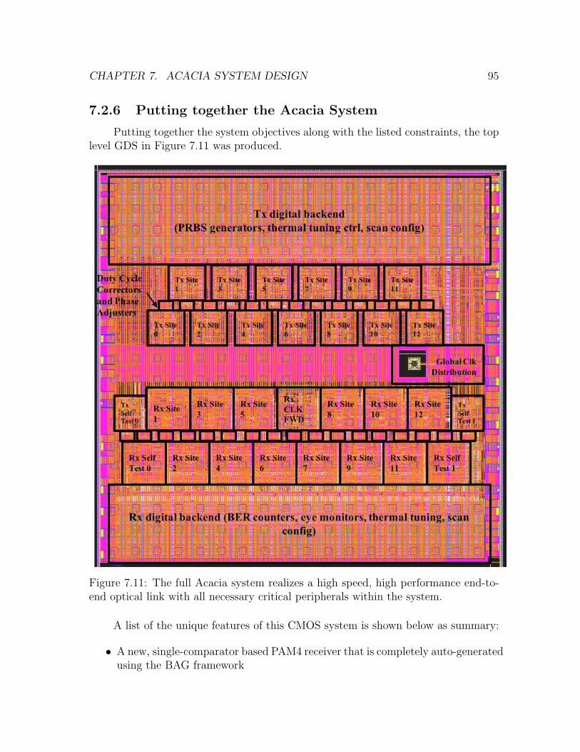
CHAPTER 7. ACACIA SYSTEM DESIGN 95
7.2.6 Putting together the Acacia System
Putting together the system objectives along with the listed constraints, the toplevel GDS in Figure 7.11 was produced.
Figure 7.11: The full Acacia system realizes a high speed, high performance end-to-end optical link with all necessary critical peripherals within the system.
A list of the unique features of this CMOS system is shown below as summary:
• A new, single-comparator based PAM4 receiver that is completely auto-generatedusing the BAG framework

CHAPTER 7. ACACIA SYSTEM DESIGN 96
• A new, thermal tuning scheme that relies on the data port and does not requirea separate drop-port filter for ring stabilization.
• Full, end-to-end characterization and supporting backends of the links (i.e.PRBS generators, BER checkers)
• On chip oscillator and clock distribution network for the high speed macros
• Duty cycle correctors and phase adjusters per front-end macro
• On chip heater drivers for ring thermal tuning
The self test sites are located in the left and right sides of the macro. The dutycycle adjusters and phase shifters are located in the smaller blocks in between the rowsof Rx sites. Each AFE has an appropriately designated Rx duty cycle corrector block.Additionally, the global clock distribution site, which contains an LO as well as theability to bypass the LO generation with an external clock, is located in between theTx and Rx macros. The output of the clock distribution network is fed into the Txand Rx macros independently. The clocks go through a localized clock distributionnetwork within each macro which buffers and cleans up the clock signal as necessary.
7.3 Results
7.3.1 On-Chip Clock Network
To validate the fidelity of the on chip LO as well as the clock distribution network,a sweep of the DAC configuration codes to adjust the LO clock frequency was initiallyperformed. In this test, the capacitive DAC of the LO output was swept. In doing so,the output frequency of the global clock distribution block was modified. The clock,in turn, propagated through the clock tree, duty cycle correctors, Rx AFE where itwas divided down, and then through the flop-synchronization logic prior to enteringthe backend. Within the backend, a counter was used in order to back-calculate thefrequency of the global clock distribution block.
Figure 7.12 shows the output clock frequency of the global clock network. Theglobal clock distribution network contains a divider which is controlled by the globalscan configuration network. This divider allows the output clock to either be undi-vided or divided by 2. Indeed, the nominal clock frequency is targetted to around 10to 12GHz. However, the maximum permissible speed of the backend (without failurein either the clock distribution network or the backend itself) required the dividerratio be set to 2. Thus, the frequencies shown in Figure 7.12 are between 5.6 and6.6GHz.
To further characterize the fidelity and quality of the incoming clock signal, aphase noise and jitter measurment was also conducted. In this case, three variants of

CHAPTER 7. ACACIA SYSTEM DESIGN 97
Figure 7.12: By modifying the capacitive DAC code, the output frequency of theglobal clock distribution can be modified according to the plot above.
inputs were studied and characterized. In the first test, a simple phase noise and jittermeasurement was done on a direct feed-through path between the exteral clock sourceand the phase noise spectrum analyzer. Next, a test wherein the external clock is fedinto the Acacia chip, then a divided clock was fed out into the spectrum analyzer wasset up. Lastly, an “unlocked” LO was activated and the output clock frequency (asfound by measuring the divided clock path) was measured and characterized. In thislast test, the “unlocked” refers to a free-running oscillator test set up. As such, thejitter measurement takes into account the frequency drift of the clock signal.
To summarize these results, the result of the first test case shows about 130fsof accrued jitter. The external clock path case (test 2) showed about 30ps. Lastly,the LO activated clock jitter was 140ps. Notice that the jitter takes into account notonly the clock source (either external or LO) jitter but also the divider and pad driverjitters. Additionally, the free running nature of the LO causes frequency shifts to beseen as jitter noise. Thus, when locked, the effective jitter will be far less for the LOcase.

CHAPTER 7. ACACIA SYSTEM DESIGN 98
7.3.2 Rx AFE and Self Test Characterization
Rx AFE signal fidelity characterization was done using the photodiode emulationcircuit (PDE) detailed in the last section. In this case, the optimal PDE current aswell as the offset for the AFE signal path were adjusted manually. Once adjusted, aBER measurement was taken using the snapshot outputs of the Rx digital backend.
To characterize the MSB data path alone (i.e. operate the receiver in NRZ modeinitially), the offset codes were adjusted in such a way as to yield the edge of a bathtub curve for low data rates. Figure 7.13 shows the low frequency sweep. In this case,the input current from the PDE was fixed at 20µA peak-to-peak.
Figure 7.13: The link’s performance is shown for low frequency and operating inMSB-mode.
The initial test to validate the TDC-based receiver was conducted at 10Gbps(collectively for both MSB and LSB streams). In this test, the MSB path was pro-grammed in such a way as to yield a 10−5 BER (as shown by the vertical dashed linein Figure 7.13. The offsets and minimum PDE current were both adjusted in such away as to yield the target BER at 5Gbps (for MSB alone). Then, the phase offset ofthe TDC-parked clock was adjusted.
The offset code, as can be seen by Figure 7.14, sweeps the location of Φ withrespect to the data path. Notice that if the clock is parked before the opening of theTDC eye, the resulting BER will show garBAGe. Similarly, if the clock is parkedafter the eye opening, the BER will be garage again. However, in between this area,when the clock is parked in such a way as to distinguish between the slow and fast

CHAPTER 7. ACACIA SYSTEM DESIGN 99
Figure 7.14: The link’s performance is shown for low frequency and operating inMSB-mode.
evaluations, the BER of the LSB data path shows a working link. Thus, at this point,the BER of the LSB data path easily hits the 10−5 BER.
7.3.3 25.6Gbps Self Test Link
A 6.4GHz clock was fed into the Acacia System’s Rx macro backend, with thegoal of creating a 25.6Gbps link. In this circumstance, the on-chip LO was activatedand programmed to output a 6.4GHz clock. The PDE codes were set in such away as to produce a peak to peak current of 90µA. From here, the bathtub curveswere measured based on the snapshot outputs produced by the digital backend. Theresulting bathtubs are shown in Figure 7.15.
Figure 7.15 shows individually the bathtub curves of both the LSB and MSBslices. In this case, the floor of the BER was limited due to the rate of snapshotupdating as opposed to any fundamental performance limit imposed by the AFEitself. Moreover, the bathtub shows flat openings for both these eyes for a substantialrange of the unit interval. The asymettry in the LSB BER curve is partially due tolack of correction abilities in both the clock phase of the on chip phase adjusters aswell as due to an offset correction bug which limited the maximum correction ability.In spite of these issues, the two curves still show promising openings.
7.4 Conclusion
The new single comparator PAM4 receiver was tested and designed in the AcaciaSoC. This chapter summarizes the various physical design trade-offs when designingand instantiating this architecture. Aside from having just the receiver, a PAM4transmitter as well as a new drop-port less thermal tuner was also implemented. Froma receiver standpoint, the various design trade-offs in the architecture were closely

CHAPTER 7. ACACIA SYSTEM DESIGN 100
Figure 7.15: The bathtub curve of the Acacia link operating at 25.6Gbps is shown.
studied and their impact on the Rx AFE was formalized. While testing the PAM4receiver, a self-test based architecture was used to quantify the link performance.The TDC-based operation was verified by sweeping the delay of the parked clock tothe TDC flop. Additionally, the link was characterized for 25.6Gbps operation andshowed promising bathtub openings for both the MSB and LSB slices.

101
Chapter 8
Conclusion
8.1 Thesis Contributions
Silicon photonic links are extremely complicated and rely on a tight overseeingin every level of the hierarchy, beginning at the device level, going into the circuit sub-block domain, climbing up into the macro system level composed of the backend andinfrastructure, and proceeding higher into the system integration level and beyond.This dissertation focused on understanding the bridge between these various levels inhierarchy and connecting it to the optimal performance for silicon photonic links.
Chapter 3 introduced and analyzed the optical modeling framework, beginningwith a high-level link picture and slowly delving into the various sub-components.The theory and “interface” between these various blocks was also studied. Once thisfoundation was layed out, the focus shifted to the link-level, where macro-parameterswere derived and trade-offs studied. Lastly, using the framework, performance pro-jections were made which, in turn, provided insight into the direction of possiblefabrication improvements moving forward.
To further realize and validate the model methodology, Chapter 4 focused onoptimizing circuit topologies given unique system parameters. Said differently, themain objective of Chapter 4 was to propose and design circuits and systems underrealistic PDK and technology specifications. In addition, based on these unique tech-nologies, the end-to-end link performance was calculated and studied further. Theframework was applied to a 65nm, heterogenously integrated CMOS plus photonicsplatform. The resulting schematic results were also showcased. Furthermore, theswing and noise-dominated regimes of operation were introduced and specific designpoints in these spaces were used to create schematics. From this all, a frameworkwas in place which could then be used to create actual silicon designs, or intuit andengineer techniques for better circuit optimization.
Chapter 5 detailed the analysis and design of a full, end-to-end 5Gbps NRZlink in the first-ever through-oxide va-based integration technique. The chapteralso described the integration platformn and showcased the top-level design for the

CHAPTER 8. CONCLUSION 102
Electronic-Photonic Integration (EPHI) system, which was taped out and publishedin ESSCIRC 2015. Subsequent sub-blocks were then analyzed further.
In Chapter 6, the trade-offs of the PAM4 versus NRZ link within the contextof the link framework were showcased. Conclusions were drawn as to exactly whenthe traditional PAM4 architecture was superior to the NRZ architecture. Next, thesingle-comparator PAM4 architecture was introduced and proved its superiority overthe traditional architecture. By targetting and eliminating two extra comparatorsper way, the new architecture provided a much more efficient AFE design. This claimwas verified in the context of the link framework from Chapter 3. The architecture’sperformance was further analyzed from a link-level standpoint with a photonic andCMOS co-simulation.
Finally, in Chapter 7, the physical design of the single-comparator PAM4 archi-tecture drove the primary motivatoin for the Acacia SoC. In the Acacia SoC, not onlywas this technique validated, but new control schemes and high performance transmitcircuitry was also introduced. Additionally, an in depth look at the physical designtrade-offs which transcended hierarchy showed the value in having a rapid design flowin order to quickly iterate and explore the space.
8.2 Future Work and Final Thoughts
As has been reiterated throughout this document (and throughout my PhD),silicon photonics has indeed stepped up as a clear contender in enhancing the ca-pabilities of CMOS technologies. For the past five years, I have been studying andplaying within this landscape and to understand these hierarchical trade-offs enoughto project better performance and also provide designer’s insights to reduce the pain oftaping out and testing these massively complex systems. However, it is clear from theconclusion of my dissertion that although many questions were answered and designapproaches were made concrete, the “show still goes on”. There are an uncountablenumber of questions which emerged from my work and even more foundations fordissertations.
To enumerate a few possible future directions, we can begin by understandingthe context and bounds of the existing link framework. Indeed, in this dissertation,we primarily focused on single-λ links and optimizing end-to-end performance thattakes into account both the transmit and receive sides. However, a logical next stepof this framework is to study and optimize end-to-end WDM links. WDM linkshave the benefit of realizing very high bandwidth densities. For the context of thiswork, we presumed that simply cascading single-λ links impose minimal secondaryeffects on adjacent channels. However, formalizing these trade-offs within the linkframework will truly promise the best end-to-end link performance while potentiallyexposing critical performance bottlenecks. Factors like resonance spacing, thermalfluctuations, and many more can be taken into account to further this research.

CHAPTER 8. CONCLUSION 103
Another interesting avenue stems from utilizing existing machine learning frame-works to truly optimize and close the design loop. Because BAG gives designers rapidaccess to generating new layouts and running/parsing post-extracted results, one mayfind benefit in generating BAG-based training sets and applying machine learningtechniques to optimize the design. Although existing work in this area uses machinelearning as a glorified optimizer, it is foreseeable that with proper circuit abstraction,true “learning” may take place and new topologies or techniques may emerge.
Lastly, the definition of “end-to-end” may indeed be brought into question. Trulyend-to-end might imply going from theory, to design, to post-extracted results, to evenphysical characterization. One may indeed aim to bring in physical experimentalcharacterization into the loop. Imagine that, at the push of a button, a designeris able to generate not only a schematic and layout, but also FPGA-bit files and alist of test equipment necessary to characterize the physical chip. Additionally, anall encompassing end-to-end characterization framework may take into account theFPGA setup, clock source jitter, etc. in order to characterize (pre-tape out) theexpected behavior from the chip. Obviously, this may be used to close the loop andmodify schematic designs accordingly.
These are just a few examples of the many research paths that this work opensthe door to. Thankfully, that chapter in my life has come to a close and I leave itto the reader of this work to make steadfast progress in one of the many directionsmade apparent throughout this dissertation.

104
Bibliography
[1] Settaluri, Krishna T., et al. ”First principles optimization of opto-electronic com-munication links.” IEEE Transactions on Circuits and Systems I: Regular Papers64.5 (2017): 1270-1283.
[2] Andrade, Nicolas M., et al. ”Optical Antenna NanoLED Based Interconnect De-sign.” 2018 IEEE Photonics Conference (IPC). IEEE, 2018.
[3] Settaluri, Krishna T., et al. ”Demonstration of an optical chip-to-chip link in a3D integrated electronic-photonic platform.” European Solid-State Circuits Con-ference (ESSCIRC), ESSCIRC 2015-41st. IEEE, 2015.
[4] Chang, Eric, et al. ”An Automated SerDes Frontend Generator Verified with a16NM Instance Achieving 15 GB/S at 1.96 PJ/Bit.” 2018 IEEE Symposium onVLSI Circuits. IEEE, 2018.
[5] Krishnamoorthy, Ashok V., et al. ”Computer systems based on silicon photonicinterconnects.” Proceedings of the IEEE 97.7 (2009): 1337-1361.
[6] Miller, David Device Requirements for Optical Interconnects to Silicon Chips,Proc. IEEE 97, 1166 - 1185 (2009)
[7] Georgas, Michael, et al. ”Addressing link-level design tradeoffs for integrated pho-tonic interconnects.” Custom Integrated Circuits Conference (CICC), 2011 IEEE.IEEE, 2011.
[8] Li, J., et al. ”Scaling Trends for Picojoule-per-Bit WDM Photonic Interconnectsin CMOS SOI and FinFET Processes.”
[9] Jung, Kwangmo, Yue Lu, and Elad Alon. ”Power analysis and optimization forhigh-speed I/O transceivers.” Circuits and Systems (MWSCAS), 2011 IEEE 54thInternational Midwest Symposium on. IEEE, 2011.
[10] Zheng, Xuezhe, et al. ”Ultra-low power arrayed CMOS silicon photonictransceivers for an 80 Gbps WDM optical link.” National Fiber Optic EngineersConference. Optical Society of America, 2011.

BIBLIOGRAPHY 105
[11] Proesel, Jonathan, Clint Schow, and Alexander Rylyakov. ”25Gb/s 3.6 pJ/band 15Gb/s 1.37 pJ/b VCSEL-based optical links in 90nm CMOS.” 2012 IEEEInternational Solid-State Circuits Conference. IEEE, 2012.
[12] Li, Cheng, et al. ”A ring-resonator-based silicon photonics transceiver withbias-based wavelength stabilization and adaptive-power-sensitivity receiver.” 2013IEEE International Solid-State Circuits Conference Digest of Technical Papers.IEEE, 2013.
[13] Ye, Yaoyao, et al. ”3D optical networks-on-chip (NoC) for multiprocessorsystems-on-chip (MPSoC).” 3D System Integration, 2009. 3DIC 2009. IEEE In-ternational Conference on. IEEE, 2009.
[14] Rylyakov, Alexander, et al. ”A 40-Gb/s, 850-nm, VCSEL-based full optical link.”Optical Fiber Communication Conference. Optical Society of America, 2012.
[15] Schow, Clint L., et al. ”25-Gb/s 6.5-pJ/bit 90-nm CMOS-driven multimode op-tical link.” IEEE Photonics Technology Letters 24.10 (2012): 824-826.
[16] Pan, Huapu, et al. ”High-speed receiver based on waveguide germanium photode-tector wire-bonded to 90nm SOI CMOS amplifier.” Optics express 20.16 (2012):18145-18155.
[17] Wu, Xiaotie, et al. ”A 20Gb/s NRZ/PAM-4 1V transmitter in 40nm CMOSdriving a Si-photonic modulator in 0.13m CMOS.” 2013 IEEE International Solid-State Circuits Conference Digest of Technical Papers. IEEE, 2013.
[18] Settaluri, Krishna T., et al. ”Demonstration of an optical chip-to-chip link in a3D integrated electronic-photonic platform.” European Solid-State Circuits Con-ference (ESSCIRC), ESSCIRC 2015-41st. IEEE, 2015.
[19] Razavi, Behzad. ”Design of Integrated Circuits for Optical Communications”,Mc Graw Hill, 2003
[20] Razavi, Behzad. ”The StrongARM Latch [A Circuit for All Seasons].” Solid-StateCircuits Magazine, IEEE 7.2 (2015): 12-17.
[21] Nikolic, Borivoje, et al. ”Improved sense-amplifier-based flip-flop: Design andmeasurements.” Solid-State Circuits, IEEE Journal of 35.6 (2000): 876-884.
[22] Personick, Stewart D. ”Receiver design for digital fiber optic communicationsystems, I.” Bell system technical journal 52.6 (1973): 843-874.
[23] J. Kim, B. S. Leibowitz, J. Ren, and C. J. Madden, Simulation and Analysis ofRandom Decision Errors in Clocked Comparators, vol. 56, no. 8, pp. 18441857,2009.

BIBLIOGRAPHY 106
[24] Nuzzo, Pierluigi, et al. ”Noise analysis of regenerative comparators for reconfig-urable ADC architectures.” IEEE Transactions on Circuits and Systems I: RegularPapers 55.6 (2008): 1441-1454.
[25] Kinget, Peter R. ”Device mismatch and tradeoffs in the design of analog circuits.”IEEE Journal of Solid-State Circuits 40.6 (2005): 1212-1224.
[26] Timurdogan, Erman, et al. ”An ultra low power 3D integrated intra-chip sili-con electronic-photonic link.” Optical Fiber Communication Conference. OpticalSociety of America, 2015.
[27] Timurdogan, Erman, et al. ”An ultralow power athermal silicon modulator.”Nature communications 5 (2014).
[28] Going, Ryan, et al. ”Metal-optic cavity for a high efficiency sub-fF Germaniumphotodiode on a Silicon waveguide” Optics Express, vol .21, Issue 19, 2013
[29] Lin, Sen. Electronic-Photonic Co-Design of Silicon Photonic Interconnects. Diss.UC Berkeley, 2017.


![Novel Design for Photonic Crystal Ring Resonators Based ...jopn.miau.ac.ir/article_3046_01eb01affabdaa909e9328069782f311.pdf · employing photonic crystals [4]. In recent years, photonic](https://img.pdfslide.us/doc/110x75/5e7ed386707cf3599e6c8522/novel-design-for-photonic-crystal-ring-resonators-based-jopnmiauacirarticle304601eb01affabd.jpg)