Embed Size (px)
Citation preview
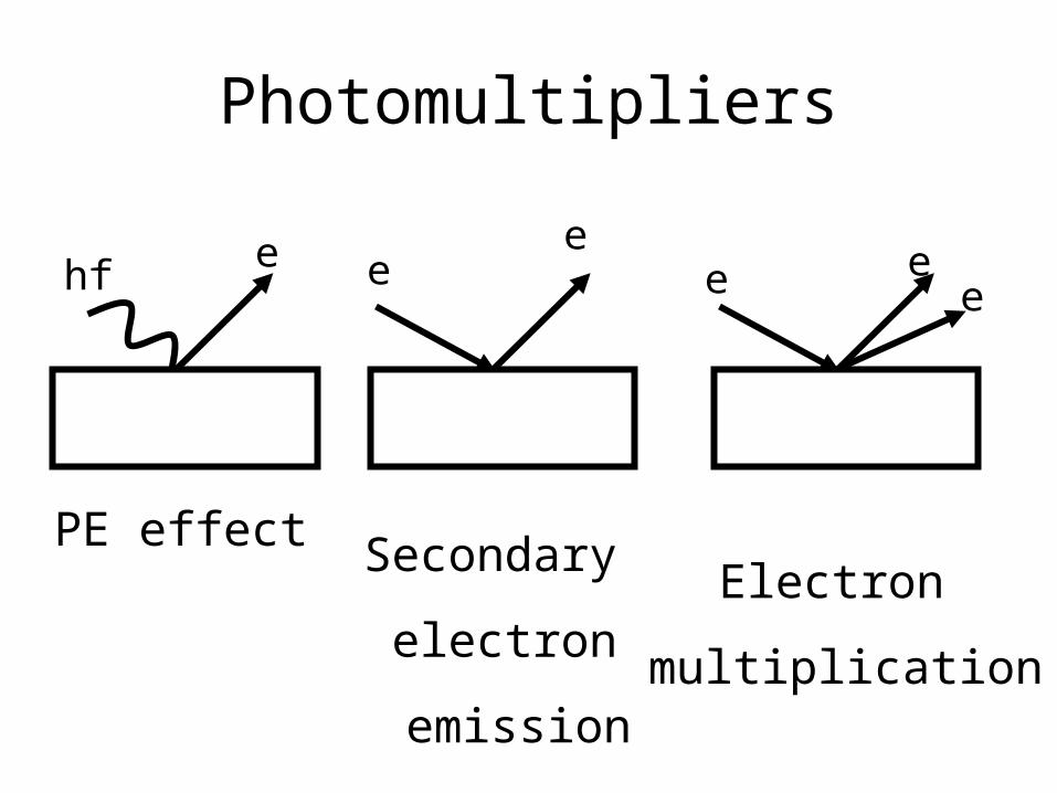
Photomultipliers
hf e ee
e ee
PE effect Secondary
electron
emission
Electron
multiplication
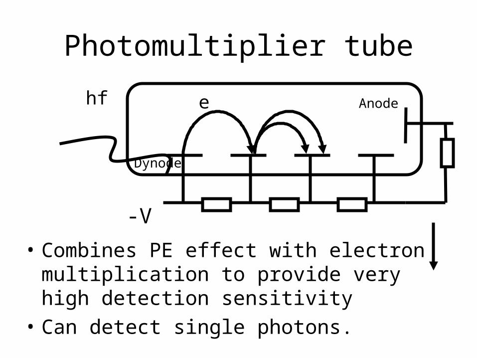
Photomultiplier tube
• Combines PE effect with electron multiplication to provide very high detection sensitivity
• Can detect single photons.
-V
hf e Anode
Dynode
Microchannel plates
• The principle of the photomultiplier tube can be extended to an array of photomultipliers
• This way one can obtain spatial resolution
• Biggest application is in night vision goggles for military and civilian use
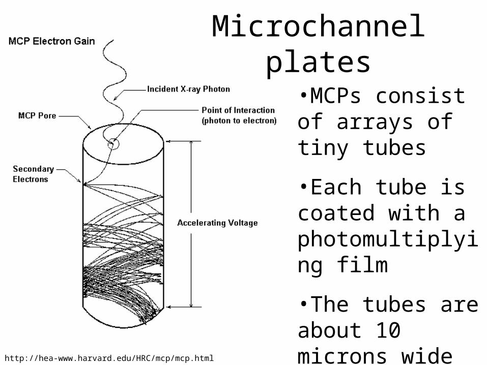
http://hea-www.harvard.edu/HRC/mcp/mcp.html
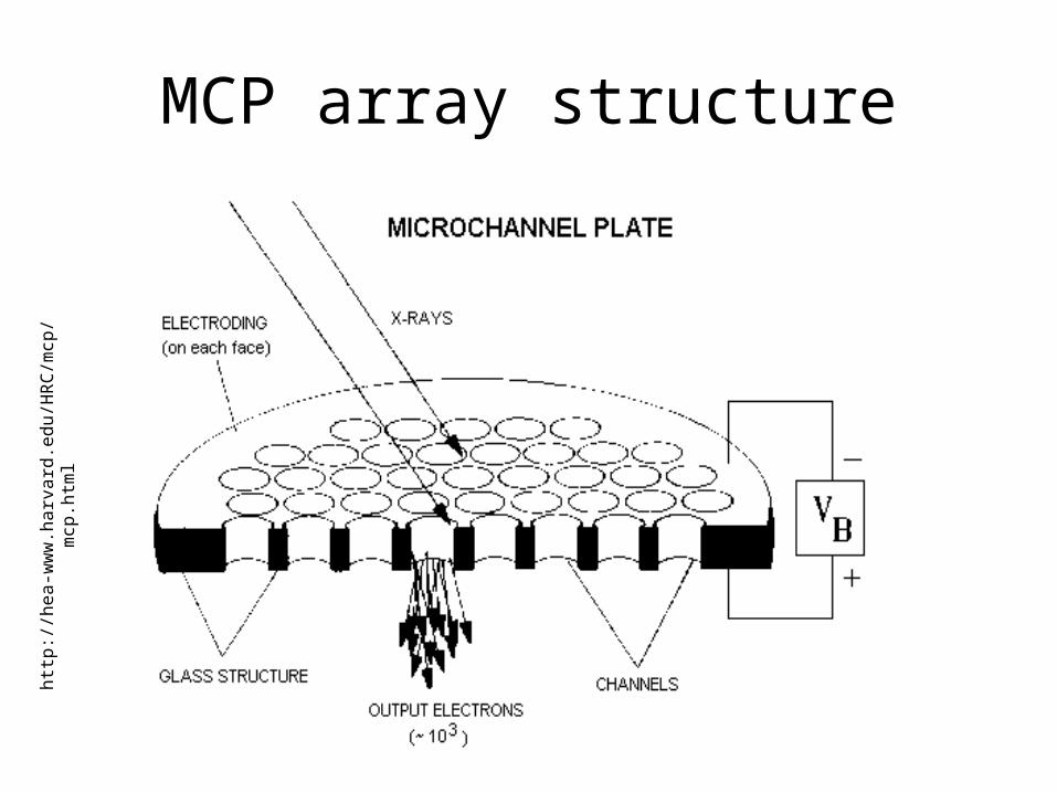
•MCPs consist of arrays of tiny tubes
•Each tube is coated with a photomultiplying film
•The tubes are about 10 microns wide
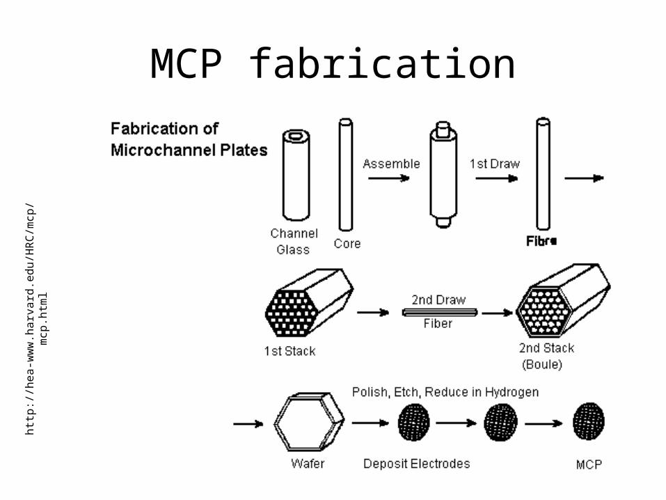
Microchannel plates
MCP array structureht
tp:/
/hea
-ww
w.h
arva
rd.e
du/H
RC
/mcp
/m
cp.h
tml
MCP fabricationht
tp:/
/hea
-ww
w.h
arva
rd.e
du/H
RC
/mcp
/m
cp.h
tml
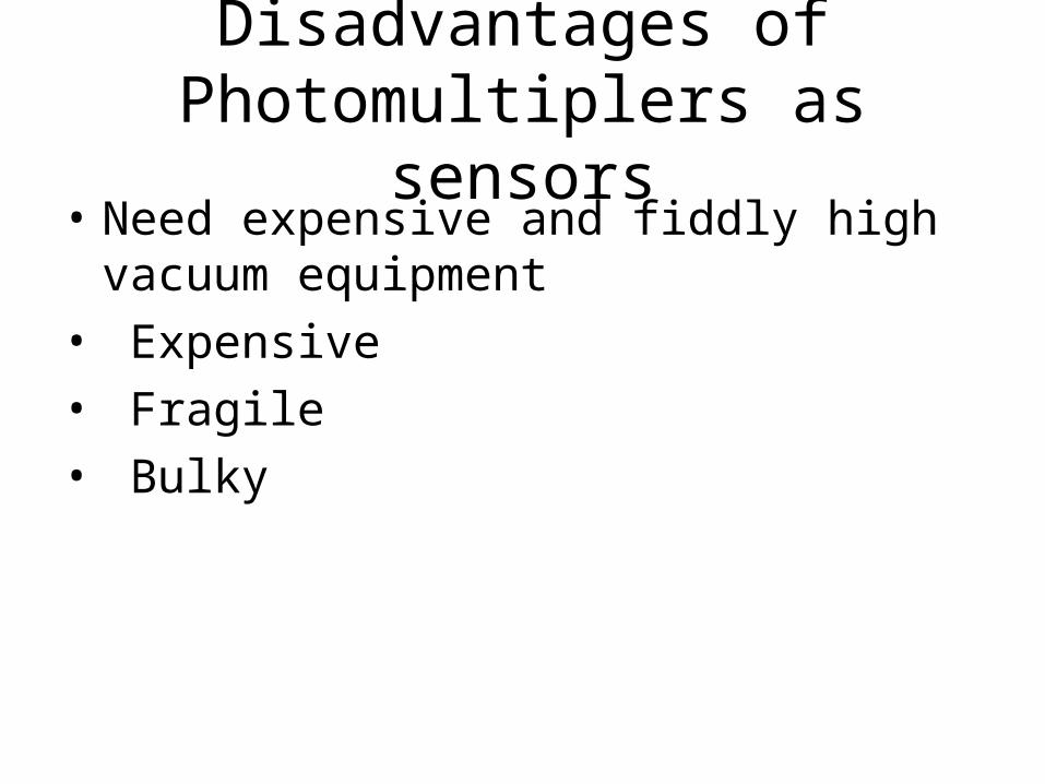
Disadvantages of Photomultiplers as sensors
• Need expensive and fiddly high vacuum equipment
• Expensive
• Fragile
• Bulky
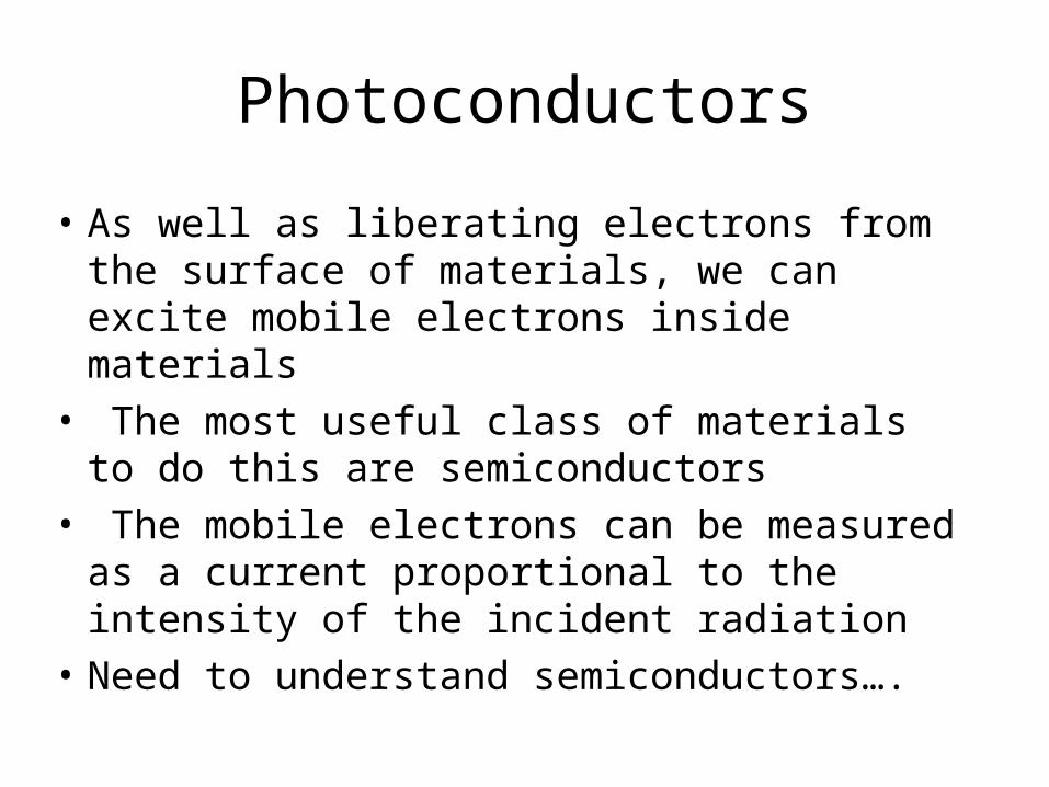
Photoconductors
• As well as liberating electrons from the surface of materials, we can excite mobile electrons inside materials
• The most useful class of materials to do this are semiconductors
• The mobile electrons can be measured as a current proportional to the intensity of the incident radiation
• Need to understand semiconductors….
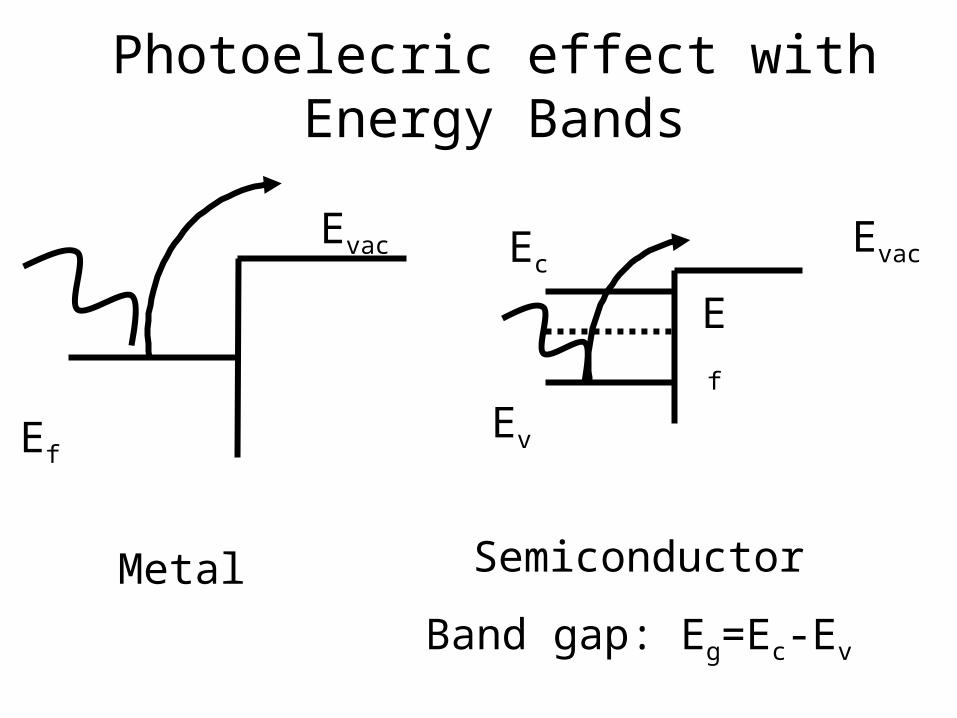
Photoelecric effect with Energy Bands
Ef
Evac
Semiconductor
Band gap: Eg=Ec-Ev
Metal
Ef
EvacEc
Ev
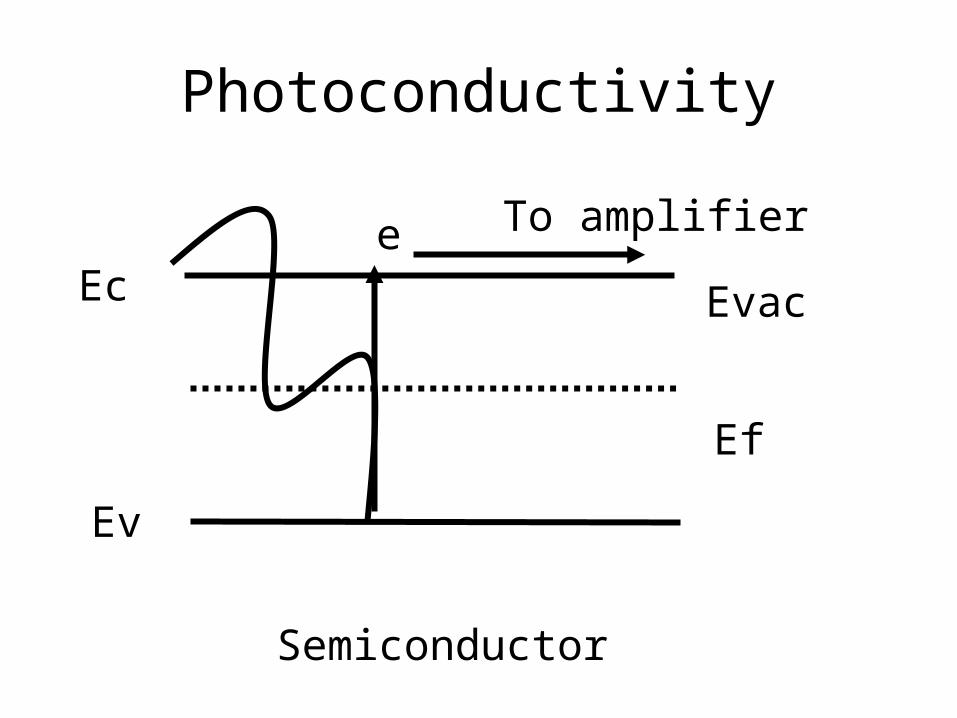
Photoconductivity
Semiconductor
Ef
EvacEc
Ev
e To amplifier
Photoconductors
• Eg (~1 eV) can be made smaller than metal work functions (~5 eV)
• Only photons with Energy E=hf>Eg are detected
• This puts a lower limit on the frequency detected
• Broadly speaking, metals work with UV, semiconductors with optical
Band gap Engineering
• Semiconductors can be made with a band gap tailored for a particular frequency, depending on the application.
• Wide band gap semiconductors good for UV light
• III-V semiconductors promising new materials
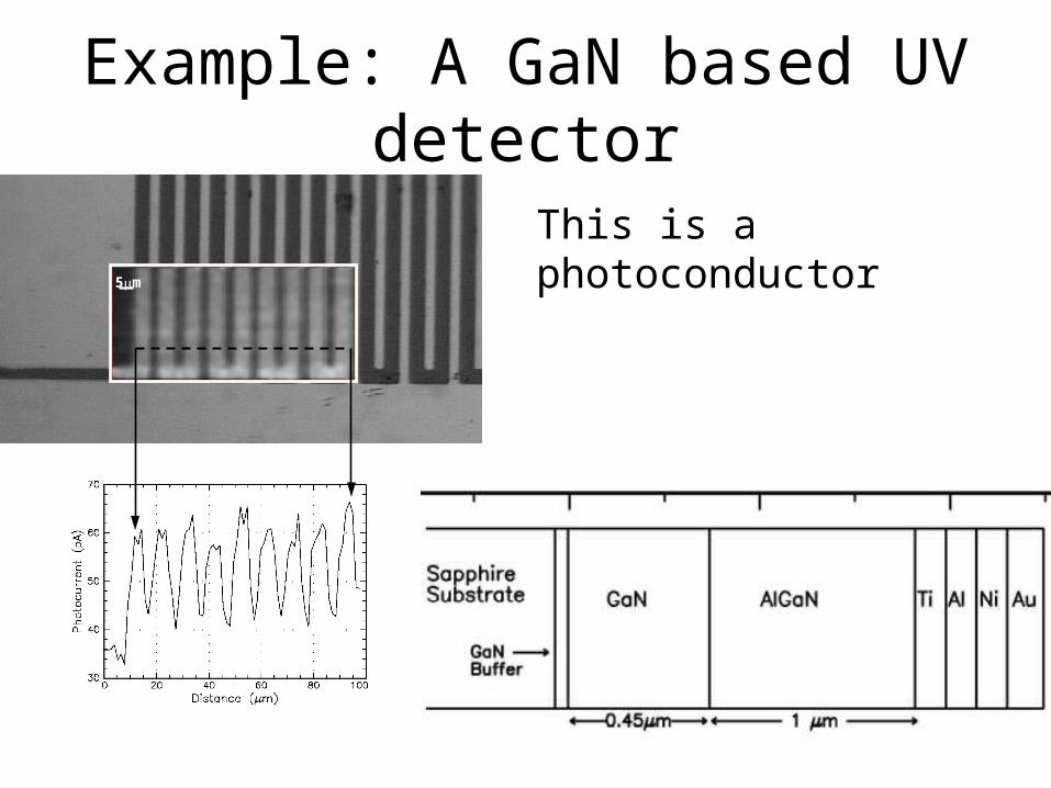
Example: A GaN based UV detector
5m
This is a photoconductor
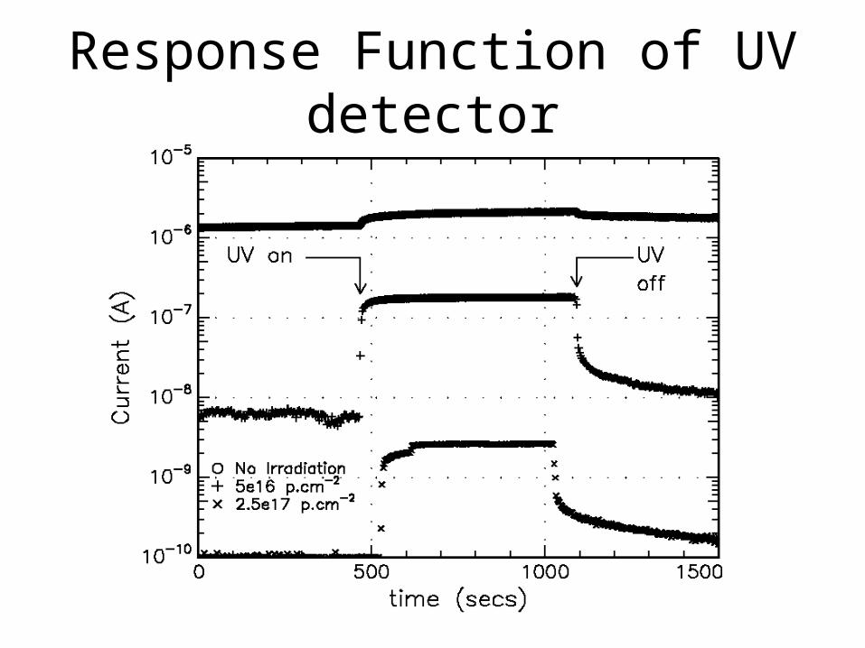
Response Function of UV detector
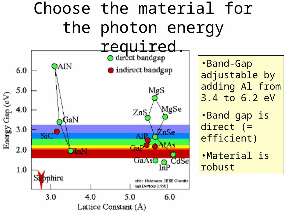
Choose the material for the photon energy required.
•Band-Gap adjustable by adding Al from 3.4 to 6.2 eV
•Band gap is direct (= efficient)
•Material is robust
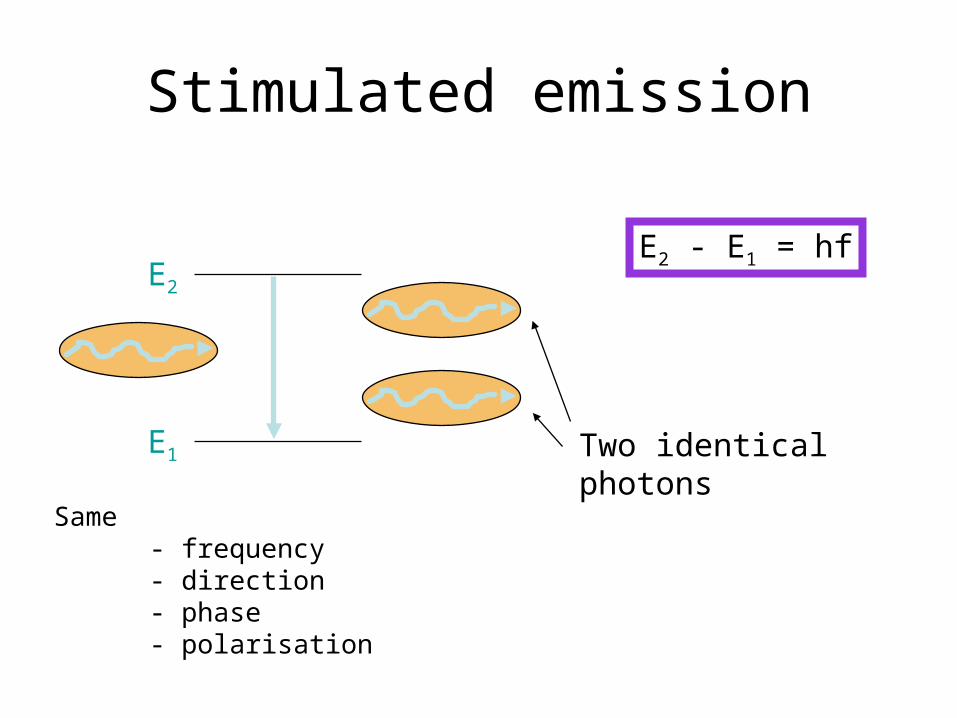
Stimulated emission
E2
E1
E2 - E1 = hf
Two identical photons
Same- frequency
- direction- phase- polarisation
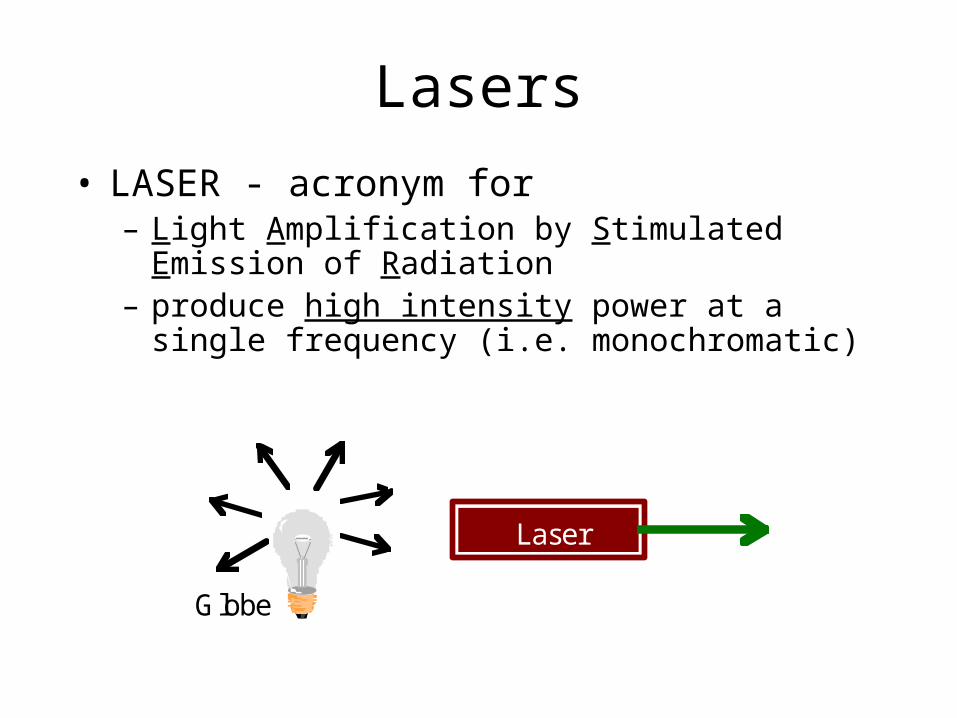
Lasers
• LASER - acronym for– Light Amplification by Stimulated Emission of
Radiation– produce high intensity power at a single frequency
(i.e. monochromatic)
Laser
Globe
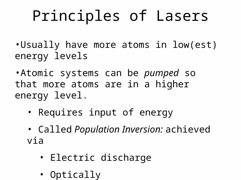
Principles of Lasers
•Usually have more atoms in low(est) energy levels
•Atomic systems can be pumped so that more atoms are in a higher energy level.
• Requires input of energy
• Called Population Inversion: achieved via
• Electric discharge
• Optically
• Direct current
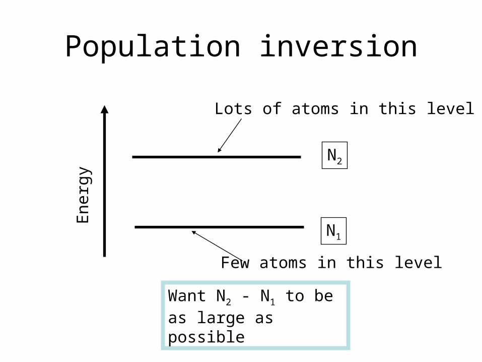
Population inversion
N2
N1
Ene
rgy
Lots of atoms in this level
Few atoms in this level
Want N2 - N1 to be as large as possible
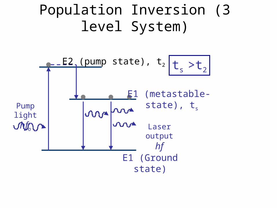
Population Inversion (3 level System)
E2 (pump state), t2
E1 (metastable- state), ts
E1 (Ground state)
Laser output
hf
Pump light
hfo
ts >t2
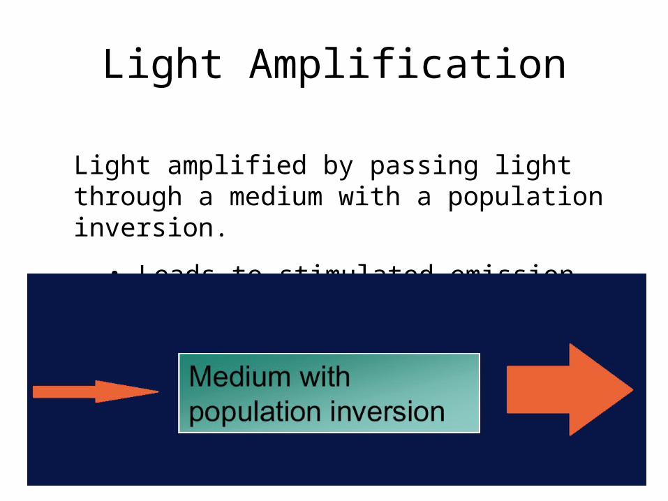
Light Amplification
Light amplified by passing light through a medium with a population inversion.
• Leads to stimulated emission
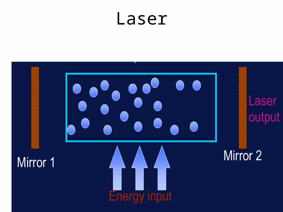
Laser
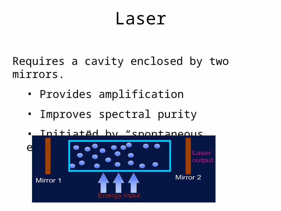
Laser
Requires a cavity enclosed by two mirrors.
• Provides amplification
• Improves spectral purity
• Initiated by “spontaneous emission”
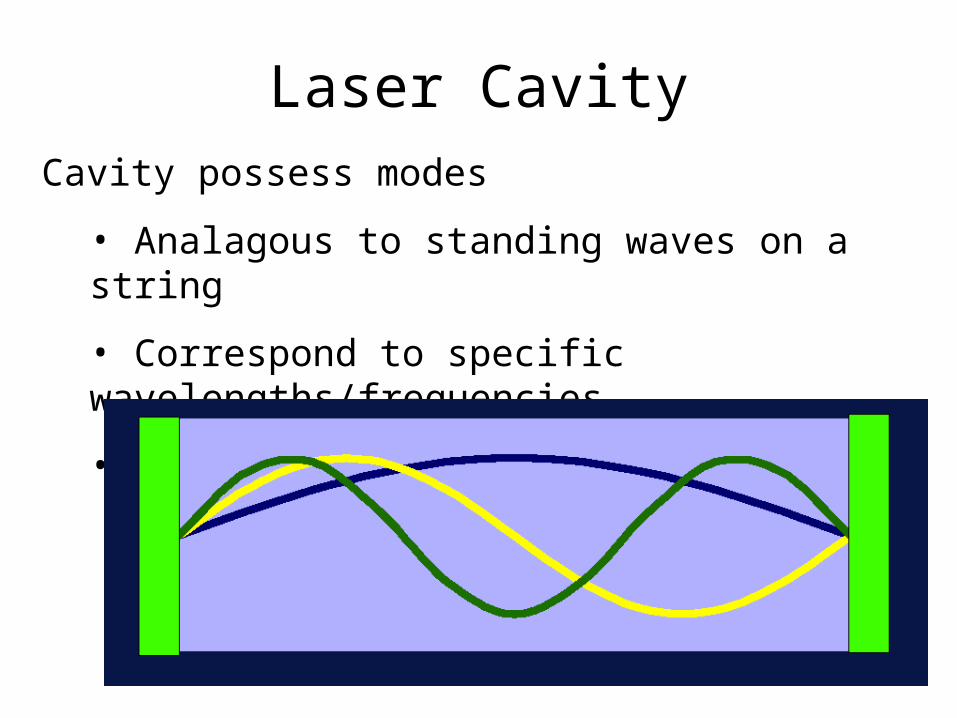
Laser CavityCavity possess modes
• Analagous to standing waves on a string
• Correspond to specific wavelengths/frequencies
• These are amplified
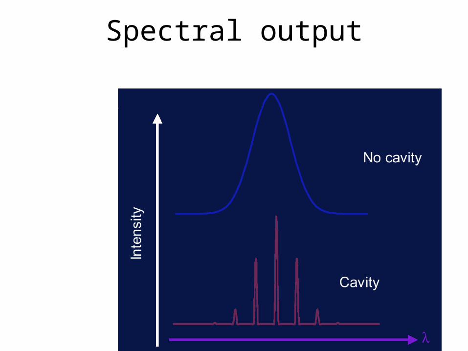
Spectral output
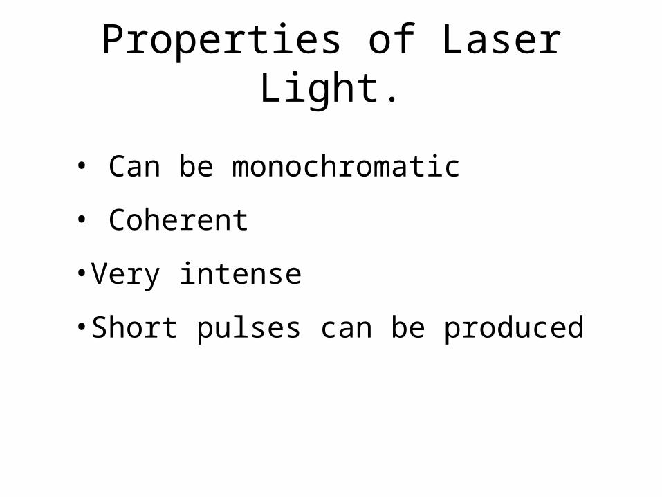
Properties of Laser Light.
• Can be monochromatic
• Coherent
•Very intense
•Short pulses can be produced
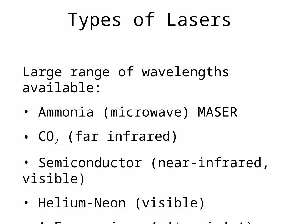
Types of Lasers
Large range of wavelengths available:
• Ammonia (microwave) MASER
• CO2 (far infrared)
• Semiconductor (near-infrared, visible)
• Helium-Neon (visible)
• ArF – excimer (ultraviolet)
• Soft x-ray (free-electron, experimental)
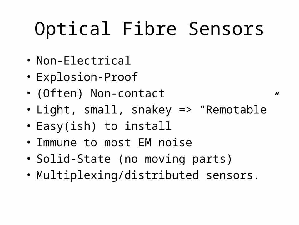
Optical Fibre Sensors
• Non-Electrical• Explosion-Proof• (Often) Non-contact• Light, small, snakey => “Remotable”• Easy(ish) to install• Immune to most EM noise• Solid-State (no moving parts)• Multiplexing/distributed sensors.
Applications
• Lots of Temp, Pressure, Chemistry
• Automated production lines/processes
• Automotive (T,P,Ch,Flow)
• Avionic (T,P,Disp,rotn,strain,liquid level)
• Climate control (T,P,Flow)
• Appliances (T,P)
• Environmental (Disp, T,P)
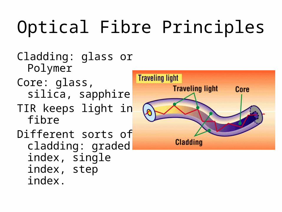
Optical Fibre Principles
Cladding: glass or Polymer
Core: glass, silica, sapphire
TIR keeps light in fibreDifferent sorts of
cladding: graded index, single index, step index.
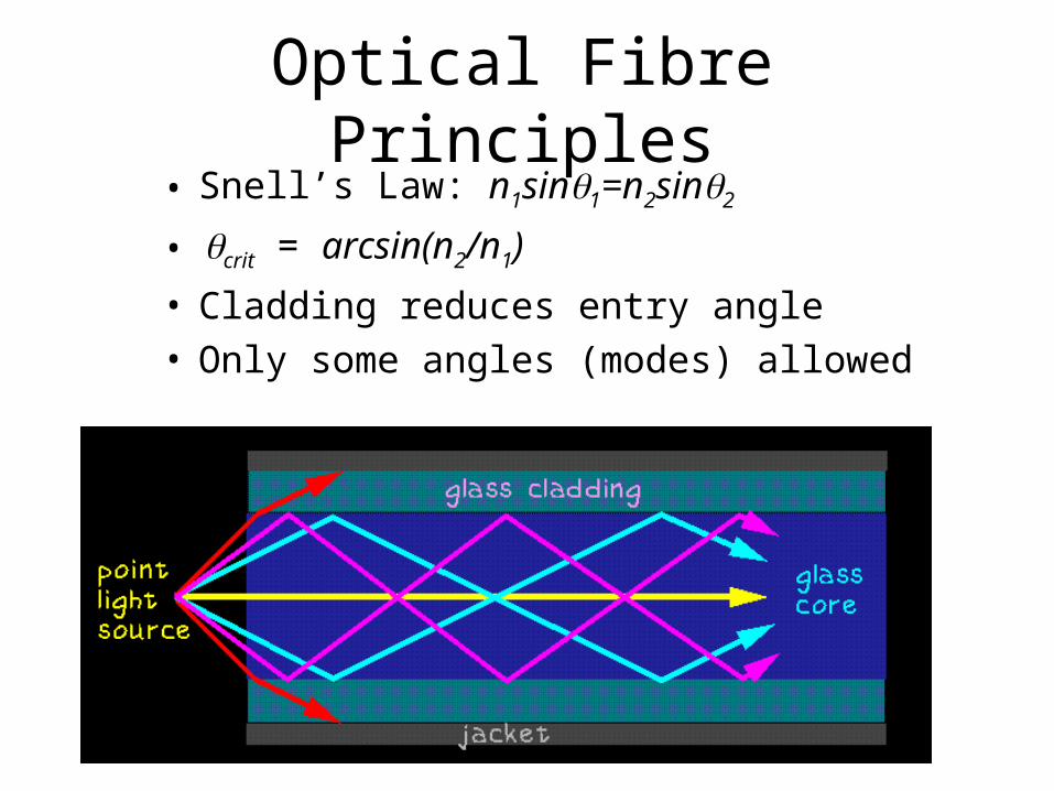
Optical Fibre Principles• Snell’s Law: n1sin1=n2sin2
• crit = arcsin(n2/n1)
• Cladding reduces entry angle• Only some angles (modes) allowed
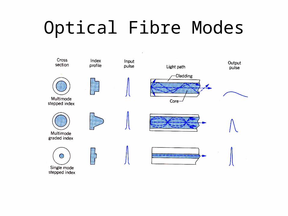
Optical Fibre Modes
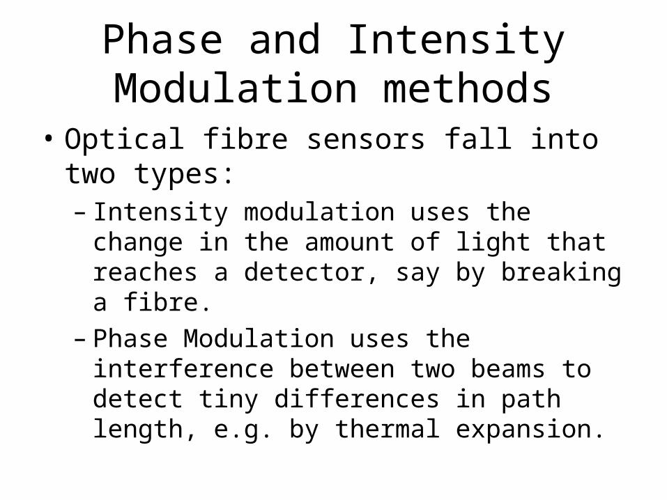
Phase and Intensity Modulation methods
• Optical fibre sensors fall into two types:– Intensity modulation uses the change in the
amount of light that reaches a detector, say by breaking a fibre.
– Phase Modulation uses the interference between two beams to detect tiny differences in path length, e.g. by thermal expansion.
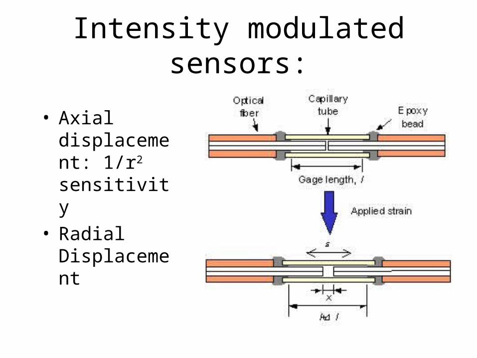
Intensity modulated sensors:
• Axial displacement: 1/r2 sensitivity
• Radial Displacement
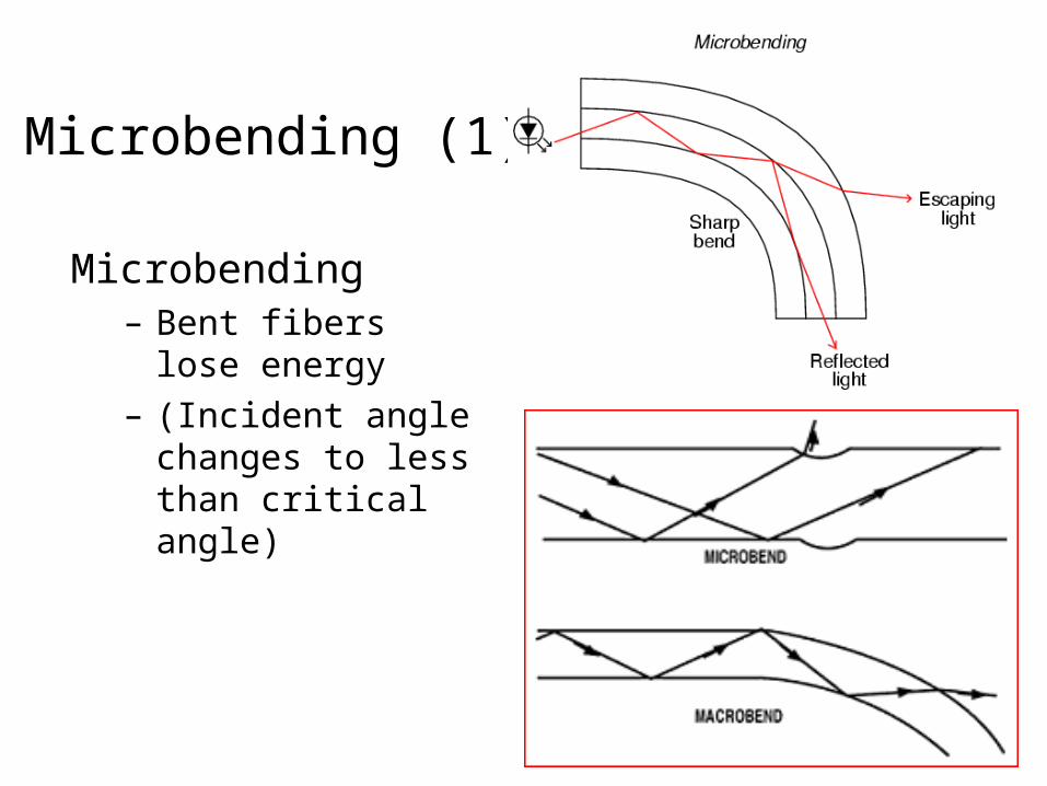
Microbending (1)
Microbending– Bent fibers lose
energy – (Incident angle
changes to less than critical angle)
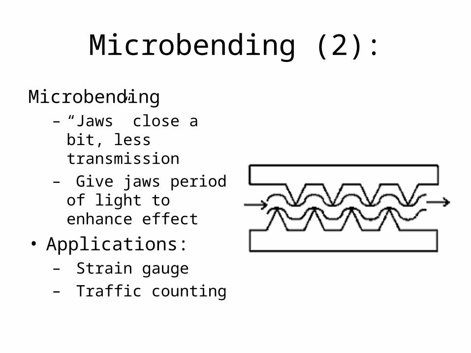
Microbending (2):
Microbending– “Jaws” close a bit, less
transmission– Give jaws period of
light to enhance effect
• Applications:– Strain gauge– Traffic counting
More Intensity modulated sensors
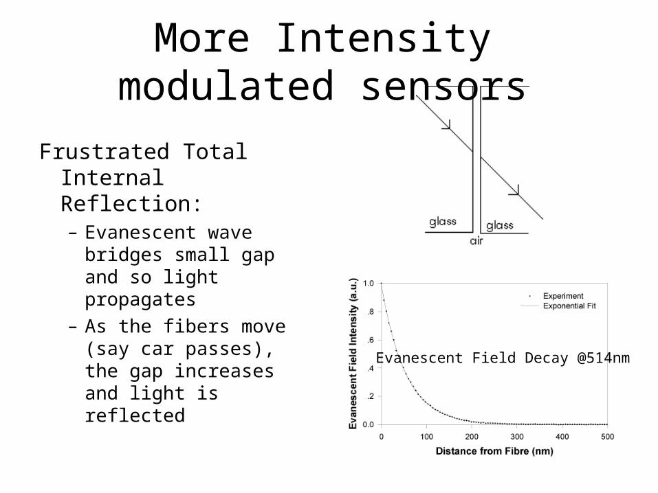
Frustrated Total Internal Reflection:– Evanescent wave
bridges small gap and so light propagates
– As the fibers move (say car passes), the gap increases and light is reflected
Evanescent Field Decay @514nm
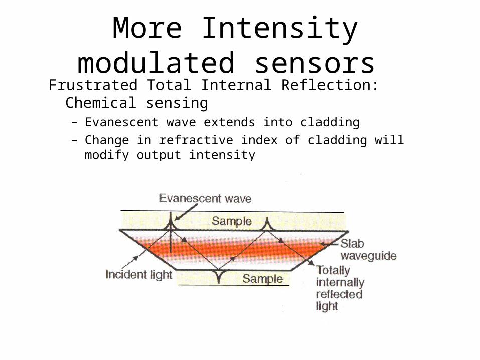
More Intensity modulated sensors
Frustrated Total Internal Reflection: Chemical sensing– Evanescent wave extends into cladding– Change in refractive index of cladding will modify output
intensity
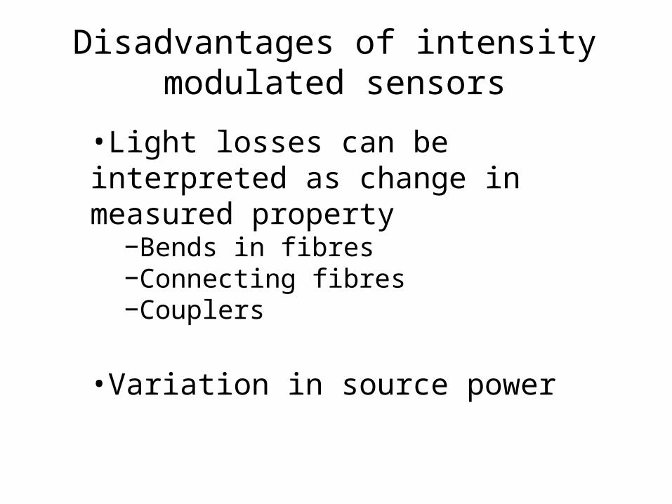
Disadvantages of intensity modulated sensors
•Light losses can be interpreted as change in measured property
−Bends in fibres−Connecting fibres−Couplers
•Variation in source power
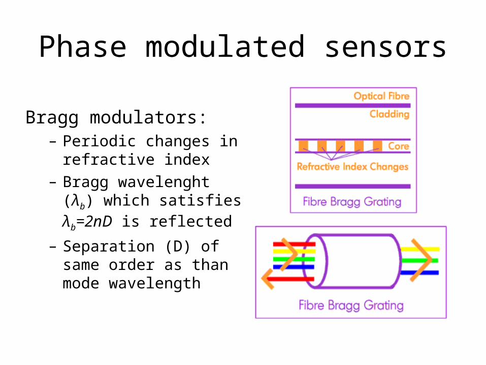
Phase modulated sensors
Bragg modulators:– Periodic changes in
refractive index
– Bragg wavelenght (λb) which satisfies λb=2nD is reflected
– Separation (D) of same order as than mode wavelength
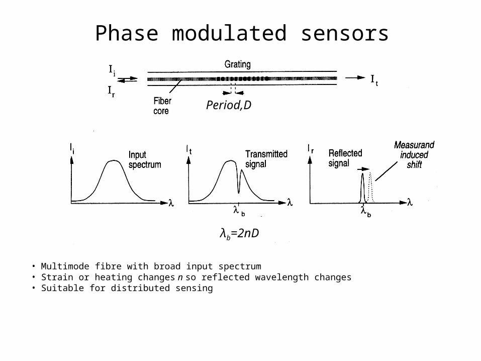
Phase modulated sensors
• Multimode fibre with broad input spectrum• Strain or heating changes n so reflected wavelength changes• Suitable for distributed sensing
λb=2nD
Period,D
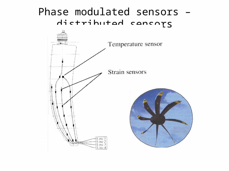
Phase modulated sensors – distributed sensors
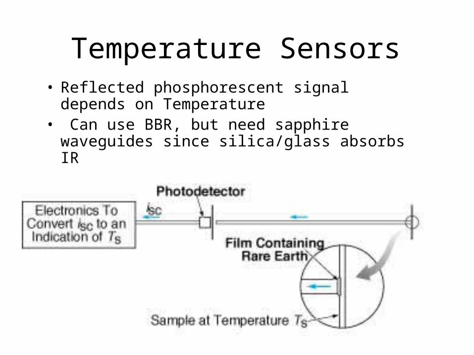
Temperature Sensors• Reflected phosphorescent signal depends
on Temperature• Can use BBR, but need sapphire
waveguides since silica/glass absorbs IR
Phase modulated sensors
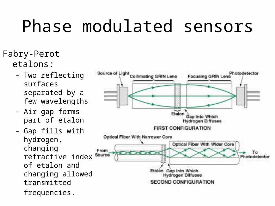
Fabry-Perot etalons:– Two reflecting
surfaces separated by a few wavelengths
– Air gap forms part of etalon
– Gap fills with hydrogen, changing refractive index of etalon and changing allowed transmitted
frequencies.
Digital switches and counters
• Measure number of air particles in air or water gap by drop in intensity– Environmental monitoring
• Detect thin film thickness in manufacturing– Quality control
• Counting things– Production line, traffic.
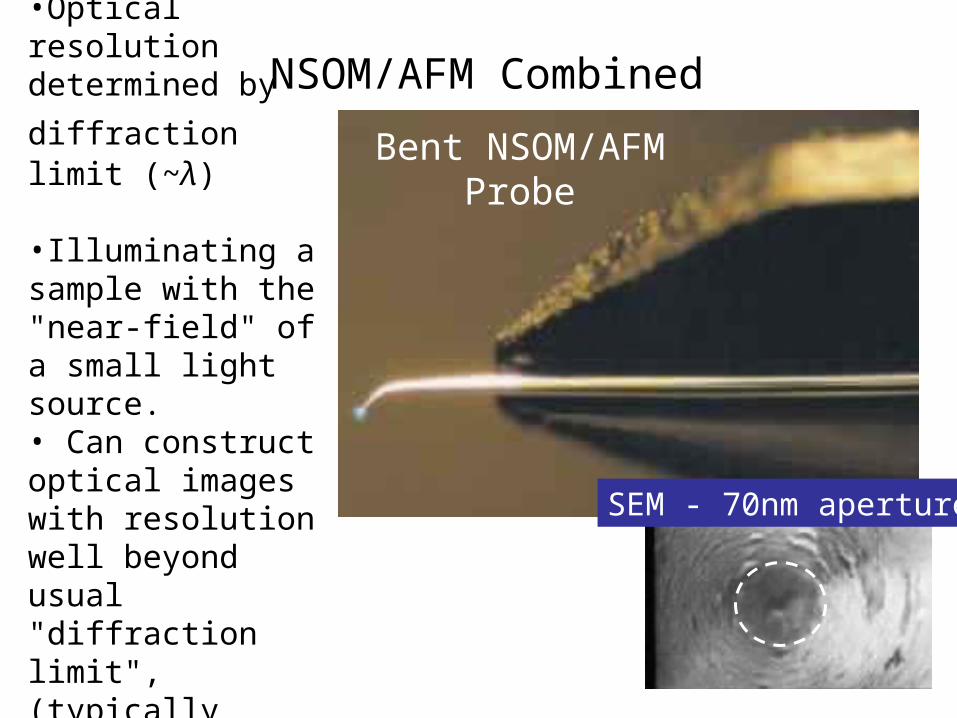
NSOM/AFM Combined
SEM - 70nm aperture
Bent NSOM/AFM Probe
•Optical resolution determined by
diffraction limit (~λ) •Illuminating a sample with the "near-field" of a small light source.• Can construct optical images with resolution well beyond usual "diffraction limit", (typically ~50 nm.)
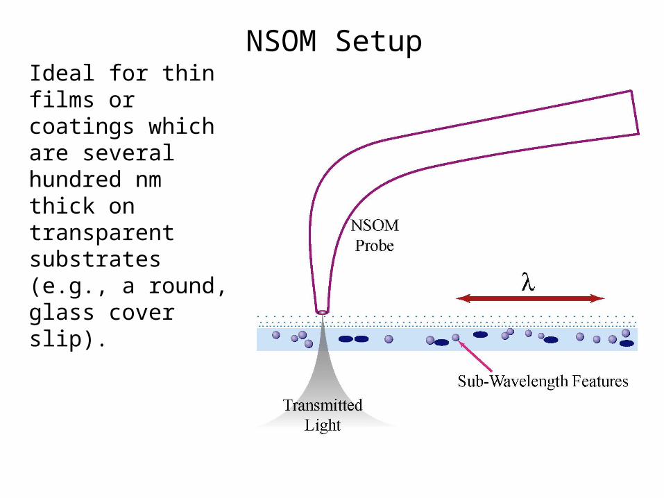
NSOM Setup
Ideal for thin films or coatings which are several hundred nm thick on transparent substrates (e.g., a round, glass cover slip).
Molecular Spectroscopy
• Molecular Energy Levels– Vibrational Levels– Rotational levels
• Population of levels• Intensities of transitions• General features of spectroscopy• An example: Raman Microscopy
– Detection of art forgery– Local measurement of temperature
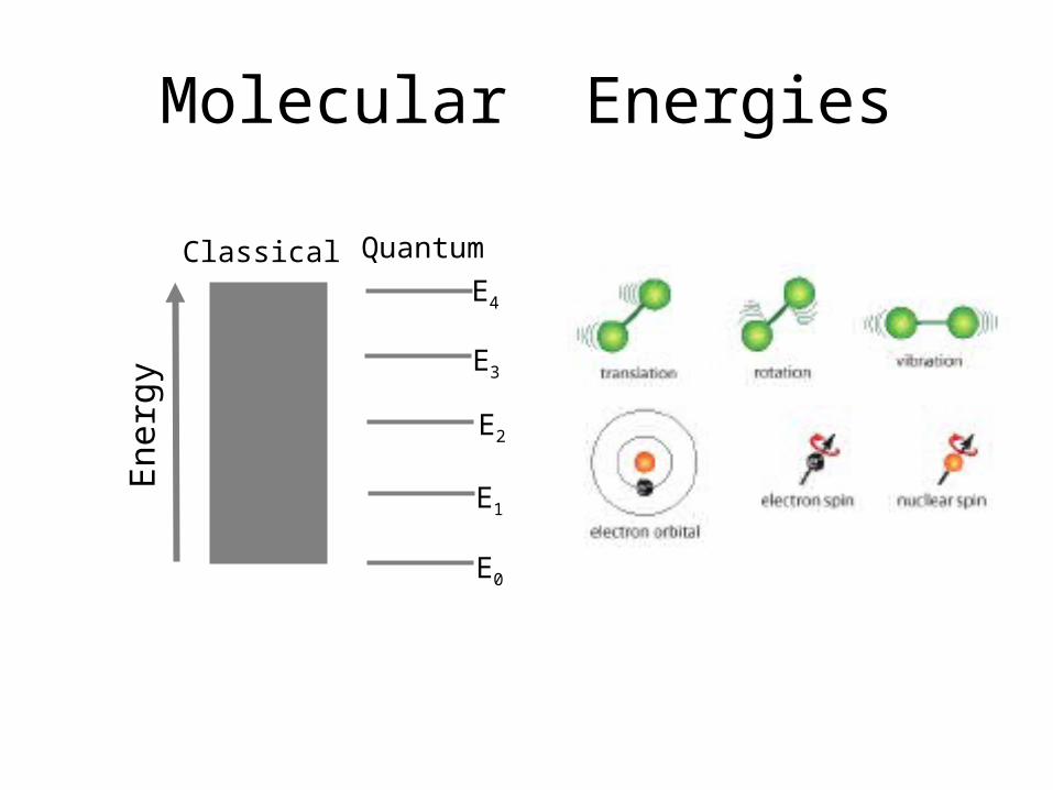
Molecular Energies
Classical Quantum
Ene
rgy
E0
E4
E3
E2
E1
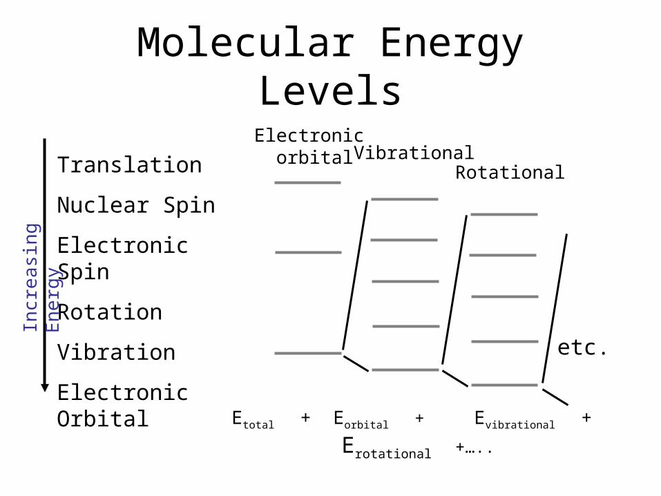
Molecular Energy Levels
Translation
Nuclear Spin
Electronic Spin
Rotation
Vibration
Electronic Orbital
Incr
easi
ng
E
nerg
y
etc.
Electronic orbital Vibrational
Etotal + Eorbital + Evibrational + Erotational +…..
Rotational
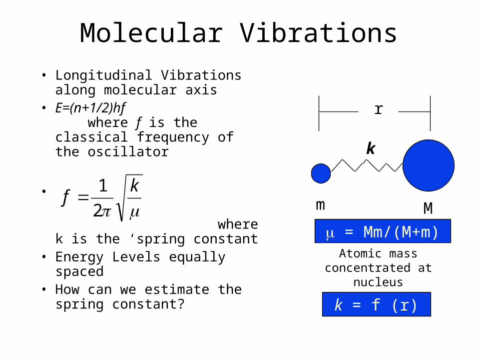
Molecular Vibrations
• Longitudinal Vibrations along molecular axis
• E=(n+1/2)hf where f is the classical frequency of the oscillator
•
where k is the ‘spring constant
• Energy Levels equally spaced
• How can we estimate the spring constant?
m M
r
k
k = f (r)
= Mm/(M+m)k
f2
1
Atomic mass concentrated at nucleus
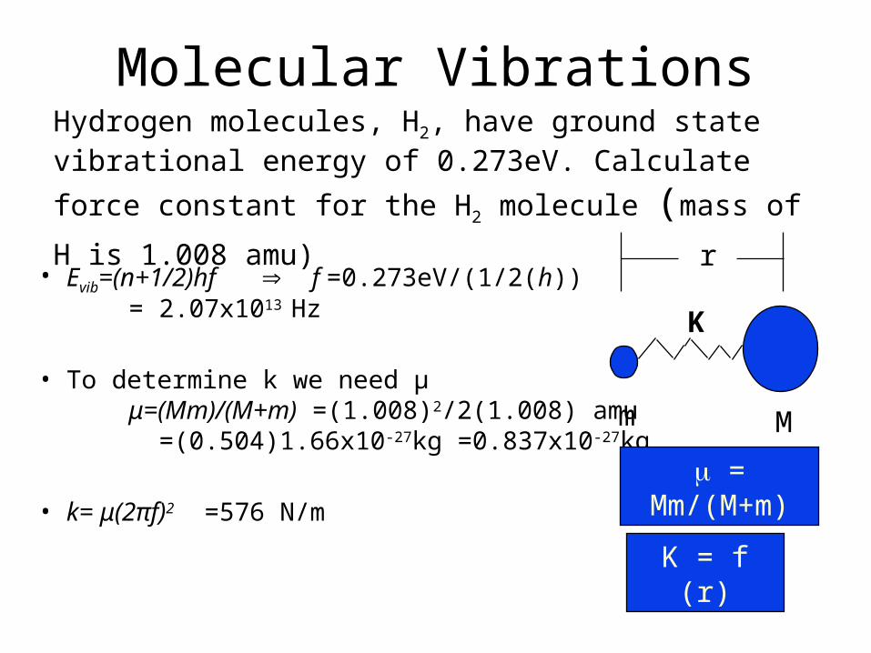
Molecular Vibrations
• Evib=(n+1/2)hf f =0.273eV/(1/2(h)) = 2.07x10¹³ Hz
• To determine k we need μ μ=(Mm)/(M+m) =(1.008)2/2(1.008) amu =(0.504)1.66x10⁻²⁷kg =0.837x10⁻²⁷kg
• k= μ(2πf)2 =576 N/m
m M
r
K
K = f (r)
= Mm/(M+m)
Hydrogen molecules, H2, have ground state vibrational energy
of 0.273eV. Calculate force constant for the H2 molecule (mass
of H is 1.008 amu)
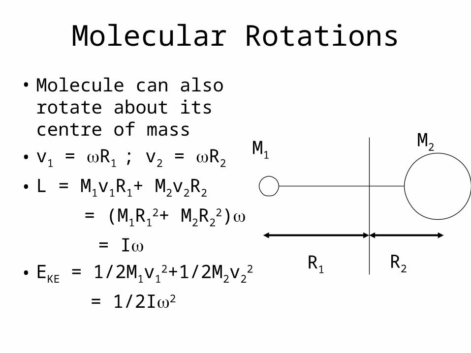
Molecular Rotations
• Molecule can also rotate about its centre of mass
• v1 = R1 ; v2 = R2
• L = M1v1R1+ M2v2R2
= (M1R12+ M2R2
2)
= I• EKE = 1/2M1v1
2+1/2M2v22
= 1/2I2
R1 R2
M1M2
Molecular Rotations
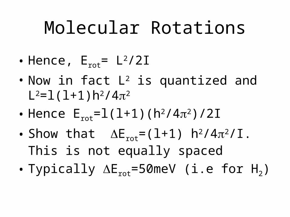
• Hence, Erot= L2/2I
• Now in fact L2 is quantized and L2=l(l+1)h2/42
• Hence Erot=l(l+1)(h2/42)/2I
• Show that Erot=(l+1) h2/42/I. This is not equally spaced
• Typically Erot=50meV (i.e for H2)
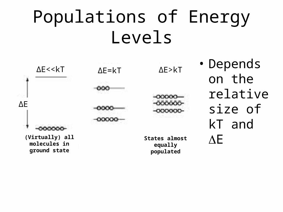
Populations of Energy Levels
• Depends on the relative size of kT and E
ΔE<<kT ΔE=kT ΔE>kT
ΔE
(Virtually) all molecules in ground
state
States almost equally populated
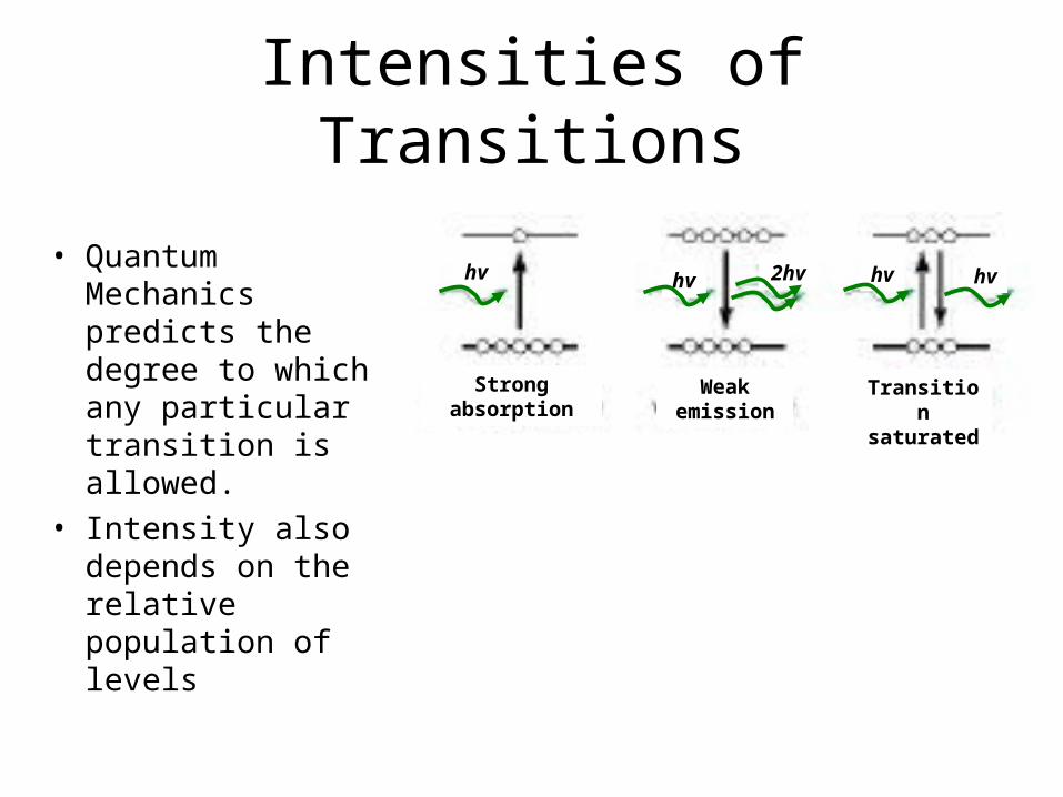
Intensities of Transitions
• Quantum Mechanics predicts the degree to which any particular transition is allowed.
• Intensity also depends on the relative population of levels
Strong absorption
Weak emission
Transition saturated
hv 2hvhv hv hv
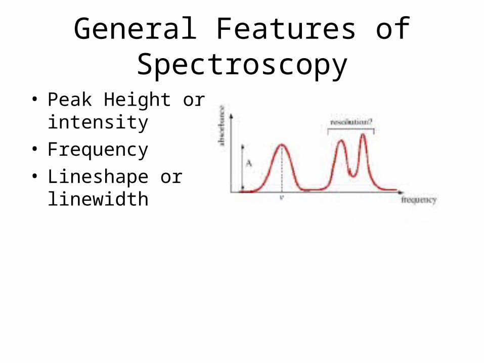
General Features of Spectroscopy
• Peak Height or intensity
• Frequency• Lineshape or
linewidth
Raman Spectroscopy
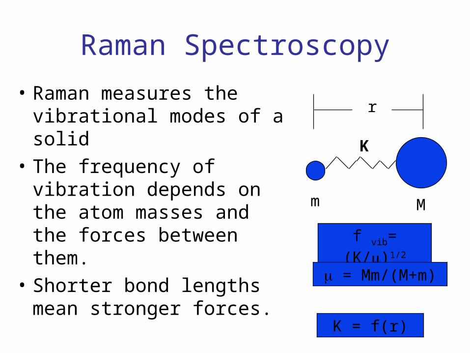
• Raman measures the vibrational modes of a solid
• The frequency of vibration depends on the atom masses and the forces between them.
• Shorter bond lengths mean stronger forces.
m M
r
K
f vib= (K/)1/2
K = f(r)
= Mm/(M+m)
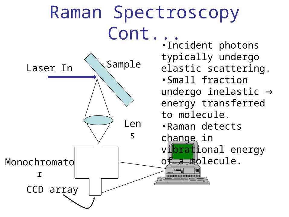
Raman Spectroscopy Cont...
Laser In Sample
Lens
Monochromator
CCD array
•Incident photons typically undergo elastic scattering.•Small fraction undergo inelastic energy transferred to molecule.•Raman detects change in vibrational energy of a molecule.
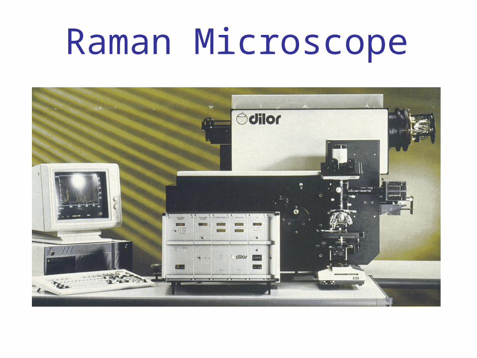
Raman Microscope
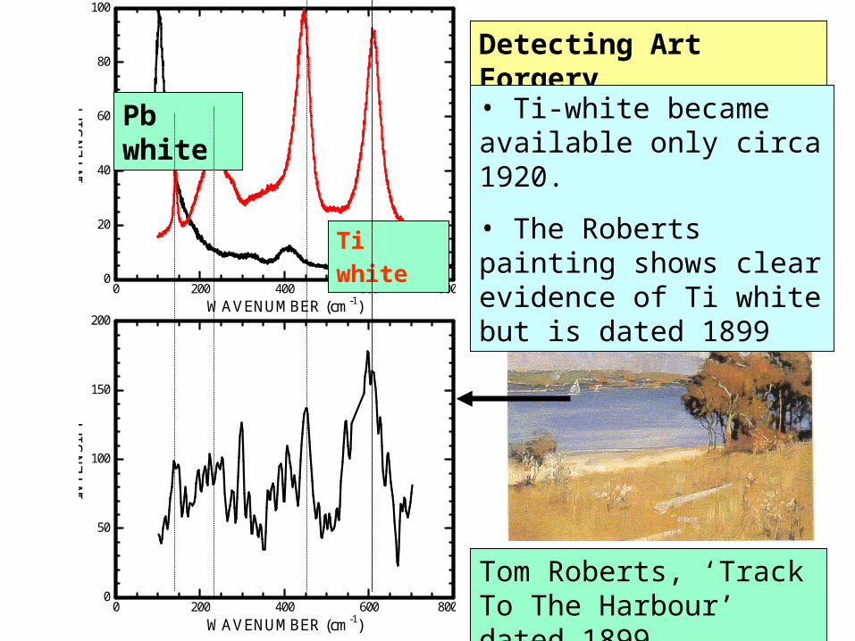
0 200 400 600 800
WAVENUMBER (cm-1)
0
20
40
60
80
100
INT
EN
SIT
Y Pb white
Ti white
0 200 400 600 800
WAVENUMBER (cm-1)
0
50
100
150
200
INT
EN
SIT
Y
Tom Roberts, ‘Track To The Harbour’ dated 1899
Detecting Art Forgery
• Ti-white became available only circa 1920.
• The Roberts painting shows clear evidence of Ti white but is dated 1899
Raman Spectroscopy and the Optical Measurement of Temperature
• Probability that a level is occupied is proportional to exp(E/kT)


![Gaseous photomultipliers and liquid hole-multipliers for future noble-liquid detectors L. Arazi [1], A. E. C. Coimbra [1,2], E. Erdal [1], I. Israelashvili](https://img.pdfslide.us/doc/110x75/56649e615503460f94b5d1ca/gaseous-photomultipliers-and-liquid-hole-multipliers-for-future-noble-liquid.jpg)