Embed Size (px)
Citation preview

PHOTOLUMINESCENCE SPECROSCOPY OF CdS AND GaSe
A THESIS SUBMITTED TO
THE GRADUATE SCHOOL OF NATURAL AND APPLIED SCIENCES
OF
THE MIDDLE EAST TECHNICAL UNIVERSITY
BY
AYŞE SEYHAN
IN PARTIAL FULFILLMENT OF THE REQUIREMENTS FOR THE
DEGREE
OF MASTER OF SCIENCE
IN
THE DEPARTMENT OF PHYSICS
SEPTEMBER 2003

iii
ABSTRACT
PHOTOLUMINESCENCE SPECTROSCOPY OF CdS
AND GaSe
Seyhan, Ayşe
M. S., Department of Physics
Supervisor: Prof. Dr. Raşit Turan
September 2003, 88 pages
With the use of photoluminescence (PL) spectroscopy one can able to get a
great deal of information about electronic structure and optical processes in
semiconductors by the aid of optical characterization. Among various compound
semiconductors, Cadmium Sulfide (CdS) and Gallium Selenide (GaSe) are
interesting materials for their PL emissions. Particularly, due to its strong anisotropy,
investigation of GaSe necessitates new experimental approaches to the PL technique.
We have designed, fabricated and used new experimental set-up for this purpose.
In this thesis, we have investigated the PL spectra of both CdS and GaSe as a
function of temperature. We observed interesting features in these samples. These
features were analyzed experimentally and described by taking the band structure of
the crystals into account. From the excitonic emissions, we determined the bandgap
energy of both materials. We studied various peaks that appear in the PL spectra and

iv
their origin in the material. We have found that donor acceptor transitions are
effective in CdS at low temperatures. A transition giving rise to a red emission was
observed and attributed to a donor level which is likely to result form an S vacancy
in CdS crystal. The PL peaks with energy close to the bandgap were observed in
GaSe. These peak were attributed to the bound excitons connected either to the direct
or indirect band edge of GaSe. The striking experimental finding in this work was the
PL spectra of GaSe measured in different angular position with respect to the crystal
axis. We observed that PL spectra exhibit substantial differences when the angular
position of the laser beam and the detector is changed. The optical anisotropy which
is responsible for these differences was measured experimentally and discussed by
considering the selection rules of the band states of GaSe.
Keywords: Photoluminescence, optical transitions, CdS, GaSe, optical anisotropy.

v
ÖZ
CdS ve GaSe’NİN FOTOLÜMİNESANS SPEKTRUMU
Seyhan, Ayşe
Yüksek Lisans, Fizik Bölümü
Tez yöneticisi: Prof. Dr. Raşit Turan
Eylül 2003, 88 sayfa
Fotoluminesans (PL) spektrumunun kullanımı ile yarıiletkenlerin elektrisel
yapıları ve optiksel oluşumları hakkında büyük ölçüde bigi edinilebilir. Kadmiyum
Sulfür (CdS) ve Galyum Selen (GaSe) ilginç PL spektrumuna sahiptir. Özellikle
GaSe’nin incelenmesi, sahip olduğu anisotropi nedeniyle, yeni deney düzenekler
gerektirmektedir. Bu tez çalışmasında bu deney düzenekleri tasarlanmış, üretilmiş ve
kullanılmıştır.
Bu tezde hem CdS hem de GaSe’nin fotoluminesans spektrumu sıcaklığa
bağlı olarak incelendi. Bu maddeler hakkında ilginç sonuçlar gözlendi. Bu sonuçlar
deneysel olarak analiz edildi ve kristallerin bant yapıları dikkate alınarak tanımlandı.
Her iki kristalin enerji bandı eksitonik ışımadan faydalanılarak belirlendi.
Fotolüminesans spektrumunda görülen çeşitli tepe değerleri ve muhtemel kaynakları
çalısıldı. Verici - Alıcı düzey geçişlerinin düşük sıcaklıklarda CdS için etkili olduğu

vi
bulundu. Kırmızı ışımada ortaya çıkan bir geçiş¸ gözlendi ve bu CdS kristali içindeki
S boşluklarından kaynaklanan verici düzeyi olarak yorumlandı. GaSe örneğinde,
enerjisi bant aralığı enerjisine yakın, fotoluminesans tepeleri gözlendi. Bu tepeler
GaSe’nin doğrudan ya da dolaylı bant kenarlarından kaynaklı bağlı eksitonlar olarak
yorumlandı. Bu çalışmadaki çarpıcı bulgu kristal eksenine göre değişik açılarda
ölçülen GaSe örneğin fotolüminesans spektrumudur. Dedektörün ve lazer ışınının
açısal konumu değiştirildiği zaman fotoluminesans spektrumunda önemli
değişiklikler gözlendi. Bu değişikliklerin nedeni olan optiksel anizotropi ölçüldü ve
GaSe örneğin bant yapısı seçme kuralları dikkate alınarak tartışıldı.
Anahtar Sözcükler: Fotoluminesans, Optiksel Geçiş, CdS, GaSe, optiksel anizotropi.

vii
ACKNOWLEDGMENTS
I would like to express my deepest appreciation to my supervisor, Prof. Dr.
Raşit Turan. Without his guidance, encouragement and support during the research,
it would have been impossible for me to complete this thesis. He has always been
ready to offer his help whenever needed.
I wish to thank all group members and technical staff in laboratory, especially
Bülent Aslan and Uğur Serincan for being so supportive to me in difficult moments,
their help in conducting experimental work and nice friendship.
I also thank Prof. Dr. Bülent Akınoğlu, Assoc. Prof. Dr. Mehmet Parlak and
Orhan Karabulut for providing samples.
I will always remember the supports, love, and understanding from my
friends; Süreyya Yıldırım, Özlem İzci, Ayla Aldemir, Tevfik Nadi Hotamış, Evrim
Uludağ, Nuray Ateş, Yasemin Sarıkaya, Nimet Uzal, Burak Uzal, İsmet Yurduşen,
Sema Yurduşen, Barış Akaoğlu. Thank you.
A deep sense of appreciation goes towards all of my family for providing me
with the endless love and support I needed to pursue and achieve my goals in life. A
very special thanks goes to İsmail Turan whose love, steadfast confidence and
constant encouragement.

viii
…TO MY FAMILY

ix
TABLE OF CONTENTS
ABSTRACT ............................................................................................................... iii
ÖZ ............................................................................................................................... v
ACKNOWLEDGMENTS ........................................................................................ vii
TABLE OF CONTENTS ........................................................................................... ix
LIST OF FIGURES ................................................................................................... xi
LIST OF TABLE ..................................................................................................... xiv
CHAPTER
1. INTRODUCTION ................................................................................................... 1
2. ELECTRONIC AND OPTICAL PROPERTIES OF SEMICONDUCTORS ........ 6
2.1. Electronic properties of semiconductors ........................................................... 6
2.1.1. Band Structure........................................................................................... 6
2.1.2. Holes in Semiconductors .......................................................................... 9
2.1.3. Band Structure of Some Semiconductors .............................................. 11
2.1.4. Intrinsic and Extrinsic Semiconductors ................................................. 17
2.1.5. Defects .................................................................................................. 25
2.2. Optical Properties of Semiconductors .............................................................. 30
2.2.1. Electrons in an Electromagnetic Field ................................................... 30
3. PHOTOLUMINESCENCE SPECTROSCOPY ................................................... 38
x
3.1. Luminescence ............................................................................................. 38
3.2. Photoluminescence ..................................................................................... 39
3.3. Recombination mechanisms ...................................................................... 41
3.3.1. Band to Band Transition ..................................................................... 42
3.3.2. Free to Bound Transition .................................................................... 43
3.3.3. Donor- Acceptor Transition ................................................................ 44
3.3.4. Free and Bound Excitons .................................................................... 45
3.4. Dependence of Photoluminescence on Laser Excitation Power ................ 47
3.5. Temperature Dependence of Photoluminescence ...................................... 50
3.6. Setup of PL ................................................................................................. 53
3.7. Experimental Techniques Used in Photoluminescence Experiments..........54
4. PHOTOLUMINESCENCE PROPERTIES OF COMPOUND
SEMICONDUCTORS CdS AND GaSe ................................................................... 56
5. CONCLUSION ..................................................................................................... 76
REFERENCES .......................................................................................................... 79
APPENDIX ............................................................................................................... 82

xi
LIST OF FIGURES
FIGURES
2.1. Crystal structure of Si .............................................................................. 11 2.2. The bandgap is 1.1 eV with the bottom of the conduction band occurring
at k=(0.852π/a,0,0) and the five other equivalent points, where a is the lattice constant (5.43 ºA).......................................................................... 12
2.3. The zincblende crystal structure of CdS. In the zincblende structure
each(Cd,S) atom is surrounded by four (S,Cd) atoms with tetrahedral symmetry ................................................................................................. 13
2.4. a. Atomic confg. of GaSe. The open and the full circles represent Se atoms,
Ga atoms, respectively. ............................................................................ 15 2.4. b. Perspective and top views of a unit of GaSe. .......................................... 15 2.5. Polytype of GaSe. Crystallographic structures of the ε, β and γ
polytypesof GaSe-like compounds. The unit cells are represented by the broken lines. They are hexagonal for the ε, β and rhombohedrical for the γ one. ........................................................................................................ 15
2.6. Band structure of GaSe .......................................................................... 17 2.7. A schematic of the density of states of the conduction and valence band.
eN and hN are the electron and hole density of states. The density of electron and holes are also shown............................................................ 18
2.8. As-doped Si crystal. The fifth valance electron of As is orbiting around its
side……………………………………………………………………...19
2.9. Energy band diagram and charge concentration in n-type semiconductors………………………………………………………….20
2.10. B doped Si crystal. Substitution of Si leads to a missing electron which is
indeed a hole ( +h ) ................................................................................... 20

xii
2.11. Energy band diagram and charge concentration in p-type semiconductor .. ................................................................................................................. 21 2.12. Energy bandgap diagram for intrinsic semiconductors with Fermi level 24 2.13. Energy bandgap diagram for extrinsic semiconductors with Fermi level
(a) for p-type, (b) for n-type..................................................................... 25 2.14. A schematic showing some important point defect in a crystal .............. 26 2.15. Shottky and Frenkel defects..................................................................... 27 2.16. Schematic presentation of a dislocation; the last row of atoms (dark) in
the inserted fractional plane ..................................................................... 28 3.1. Most common radiative transition observable with photoluminescence
and non-radiative transitions.................................................................... 40 3.2. Most common radiative transition observable with photoluminescence
and non-radiative transitions.................................................................... 42 3.3. The schematic representation of Photoluminescence set-up ................... 52
3.4. Holders..................................................................................................... 54
4.1. Photoluminescence spectrum of CdS at T~ 20 K .................................... 57 4.2. PL spectra of green band of CdS as a function of temperature ............... 58 4.3. PL spectra of the near band edge transitions of CdS as a function of
temperature .............................................................................................. 59 4.4. PL spectra of red band for CdS as a function of temperature.................. 59 4.5. Optical transition in CdS crystal .............................................................. 60 4.6. Temperature dependences of red band CdS PL intensity at the emission
band maxima............................................................................................ 62 4.7. Deconvolution of the photoluminescence spectra into Gaussian lineshapes
at ~20 K. (k//c) ......................................................................................... 64 4.8. Variation of GaSe PL intensity with reciprocal temperature, at 20 and
300 K........................................................................................................ 65 4.9. Temperature dependence of the peak energy position of the A band ...... 66 4.10. Photoluminescence spectra of undoped p-type GaSe as a function of
temperature. k//c. ..................................................................................... 67

xiii
4.11. Experimental conditions for the measurement of anisotropic PL emission.
a) Laser beam is directed to the sample surface with an angle of 45o with respect to c-axis. The detector is positioned along the c-axis (k//c). b) Laser beam is directed on the side of the sample. The detector’s position is along the direction perpendicular to the c-axis (c⊥ k). c) The detector is in the same position as b), but the laser beam falls on the sample with an angle ......................................................................................................... 69
4.12. Photoluminescence spectrum of GaSe with respect to k//c and k⊥ c axis70 4.13. Photoluminescence spectra of GaSe as a function of temperature. k⊥ c. 71 4.14. Photoluminescence spectra of GaSe as a function of temperature. k⊥ c. 71 4.15. Deconvolution of the photoluminescence spectra into Gaussian lineshapes
at~20 K .k⊥ c ........................................................................................... 73 4.16. Variation of GaSe PL intensity with reciprocal temperature, k⊥ c ......... 74 4.17. Temperature dependence of the peak energy position, k c ...................... 75
xiv
LIST OF TABLES
TABLES
2.1 Effective mass of carriers in germanium, silicon Crystal structure of Si .. 8 2.2. Fitting parameters for Germanium and Silicon ......................................... 9 2.3. Some properties of Si. All temperature dependent parameters are at
T=300K [11]. ........................................................................................... 13 2.4. Some propetties of CdS [11].................................................................... 14

1
CHAPTER 1
INTRODUCTION
During the seventies and eighties, we have witnessed remarkable advances in
our understanding of semiconductor properties and rapidly expanding uses of
semiconductor devices in industrial and consumer products. The phenomenal growth
of the semiconductor industry has resulted in a gradual increase in material research
for better, higher performance, and more reliable semiconductors. The questions
regarding degradation of semiconductor device performance rely on heavily on our
basic knowledge of semiconductor materials such as that which relates to carrier
transport, defect mechanism and impurities. For different semiconductor devices, one
needs materials with different parameters, like energy gap. Physical properties are
very different among different semiconductors due to distinct characteristics of
energy gaps and impurities. These impurities play a major role in determining the
electrical and optical properties of semiconductors. One of the most commonly used
techniques to investigate properties in semiconductors is Photoluminescence.
Photoluminescence (PL) has become a standard method for the
characterization of semiconductors properties. It combines the advantages of an
optical method, namely being non-destructive and not requiring electrical contacts,
with very high sensitivity. PL can be used to determine energy levels, concentration

2
of impurities, defects and fundamental properties of semiconductors [1, 2]. PL, more
generally all kind of luminescences, is a result of energy transition of electrons.
Photoluminescent materials are characterized primarily on the basis of the
mechanism(s) involved in (1) interband transitions, (2) transition including
impurities or defects and (3) hot carrier intraband transitions. The first category is
further broken down into near band edge band-to-band transition, and hot carrier
band-to-band transition. Second category consists of conduction band to acceptor
level, donor level to valance band, donor to acceptor level transition, free and bound
exciton transition, and deep level transition. All these transitions could result in the
emission of photon; whether this is likely or not depends on both the transition
mechanism and the material. Many other considerations serve to further complicate
this already complex topic. An electron and a hole orbit each other about their
common center of mass; this hydrogen-atom-like system is called an exciton.
Exciton can only exist for a meaningful length of time at very low temperatures.
Since the electron and the hole attract each other, an exciton has less potential energy
than a free pair of charge carriers. Thus when an exciton recombines, any photon
which is emitted has slightly less energy than the bandgap. Since this photon doesn’t
have quite enough energy to re-excite an electron from the valance band into
conduction band, it has a much better chance to escape from the crystal than photons
created by transition at or above the bandgap.
The basic difference between direct gap and indirect gap transitions is that,
unlike for indirect gap case, the maximum of valance band and minimum of the
conduction band occur for the same value of the wave number k for direct gap
transitions. Because the electron will tend to equilibrate to the lowest energy state

3
available, the top of the valance band will collect holes, as electrons move down into
available lower energy states. For the same reason, the bottom of the conduction
band will collect electrons. Thus in a material with a direct gap the k values of these
distributions overlap and photons can be emitted as carriers recombine directly. On
the other hand, in a material with an indirect gap the story is not that much simple,
since a transition from conduction band to the valance band involving only the
emission of a photon will not conserve the crystal momentum. In order for an
electron to make a transition from to conduction to the valance band, both a photon
and a phonon may be emitted thus allowing both momentum and energy to be
conserved. In this thesis we studied PL technique by conducting on compound
semiconductors Cadmium Sulfide (CdS) and Gallium Selenide (GaSe) as a function
of temperature.
Bulk cadmium sulfide has both wurtzite crystal structure, especially when
grown at high temperature and zincblende crystal structure when precipitated from
solution [3]. The Cd-S bonds in the crystal have both ionic and covalent character.
Bulk CdS is nearly always n-type semiconductors, having in their natural state a
preponderance of electron donor states near the conduction band edge [4]. The band
gap energy of CdS is given in [5] at T=300 K and T=0 K the bandgap energies are
2.53eV (491nm), and 2.58eV (481nm), respectively.
The experimental investigation of the electrical and optical properties of
GaSe has received much attention due to its possible application in photoelectronic
devices in the visible range [6]. Being a member of the group III-VI, GaSe is a layer
semiconductor whose crystal c-axis is perpendicular to the layer planes. The
sandwich layer consists of four covalently bound sheets of hexagonal close-packed

4
atoms, arranged in the sequence Se-Ga-Ga-Se [7]. Three different periodic stacking
sequence of the layers have so far been observed and have been described in the
literature as ε , γ , and β- GaSe. The ε and β- phases are 2H Hexagonal polytypes,
and the modification γ has a 3R trigonal structure [8]. The layers are bound by weak
van der Walls forces while intralayer –bonding forces are primarily ionic-covalent in
nature. The electronic band structure of GaSe shows indirect minimum of the
conduction band (CB) at the M point of the Brillouin zone which is lower (only
25meV) than the direct gap at the Γ point and they are located the top of the valance
band (VB) at the center of the Brillouin zone [9]. PL of GaSe is highly complex at
low temperature; it involves either intrinsic sharp lines because of the excitonic
recombination or extrinsic bands at lower energy related to the lattice defects or
impurities.
Organization of this thesis is as follows. In chapter 2, as a theoretical
background material to our experimental investigation, electronic and optical
properties of semiconductors are comprehensively reviewed. We particularly deal
with the basics of electrons and holes in semiconductors, band structure of
semiconductors and present further band structure for some specific semiconductors.
The properties of conduction and valance bandedge states, intrinsic and extrinsic
semiconductors and defects in semiconductors are also briefly discussed. In the last
part of this chapter we concentrate on the motion of an electron in an electromagnetic
field by focusing on its optical parameters.
In the next chapter after brief discussion of luminescence and
photoluminescence concepts, we present the recombination mechanisms such as
band to band transition, free to bound transition, donor-acceptor transition, and free

5
and bound excitons. Next the dependencies of the photoluminescence spectrum on
the parameters such as the laser excitation power and temperature are discussed
separately in a general sense. Chapter 3 is finalized by depicting a schematic
representation of a PL setup that we have used in our experimental survey.
In the subsequent chapter, chapter 4, photoluminescence properties of our
sample crystals CdS and GaSe are investigated separately. Firstly, we have carried
out PL spectroscopy of CdS in the temperature range of 0 -300 K. Set-up used in this
investigation is shown in Fig. (3.3). A series of PL peaks were observed with the
peak values located at approximately 490 nm, 696 nm, and 449nm. The bandgap of
CdS is divided into four fundamental bands which are labeled as Green, Yellow, Red
and Raman. We observed five of all peaks in the Green band. The observed peak
values are almost in agreement with those already exist in literature. There is only
one peak in red band, we interpret the peak as the one originated from deep level
created by S vacancies. The peak energy appears at 696 nm. The last peak known as
Raman, located at 449 nm in the temperature range from 130-20 K.
Secondly, PL spectrum of GaSe was studied. Having electrical and optical
anisotropy, GaSe has quite complex band structure like CdS. PL spectrum of GaSe
shows a large number of sharp lines near the band edge and wider bands away from
the band edge. This is the case since both direct and indirect transitions are likely to
occur. Free and bound exciton transitions were observed in each of direct and
indirect bandgap at 606 and 627 nm, respectively. There exists one more peak in the
temperature region 70-20 K at 647 nm. Final chapter of the thesis is devoted to our
conclusions.
6
CHAPTER 2
THEORETICAL APPROACH:
ELECTRONIC AND OPTICAL PROPERTIES OF SEMICONDUCTORS
2.1 ELECTRONIC PROPERTIES OF SEMICONDUCTORS
Semiconductor is a material whose electrical conductivity is midway
between that of an good conductor and a good insulator; a type of material having a
lower energy valence band that is nearly completely filled with electrons and a
higher energy conduction band that is nearly completely empty of electrons, with a
modest energy gap between the two bands; pure materials usually exhibit electrical
conductivity that increases with temperature because of an increase in the number of
charge carriers being promoted to the conduction band.
2.1.1 Band Structure
Energy bands consisting of a large number of closely spaced energy levels
exist in crystalline materials. The bands can be thought of as the collection of the
individual energy levels of electrons surrounding each atom. The wavefunctions of
the individual electrons, however, overlap with those of electrons which is confined
to neighboring atoms. The Pauli exclusion principle does not allow the electron
energy levels to be the same so that one obtains a set of closely spaced energy levels,
forming an energy band. The energy band model is crucial to any detailed treatment

7
of semiconductor devices. It provides the framework needed to understand the
concept of an energy bandgap and that of conduction in an almost filled band as
described by the empty states.
The analysis of periodic potentials is required to find the energy levels in a
semiconductor. This requires the use of periodic wave functions, called Bloch
functions. The description of the electron in a semiconductor has to be done via the
Schrodinger equation
( ) ( ) ( )rErrUm
ψψ =
+∇− 2
0
2
2h , (2.1)
where U(r) is the background potential seen by the electrons. The bloch theorem
gives us the form of electron wavefunction in a periodic structure and it states that
the eigenfunction is the product of a plane wave riker⋅ times a function ( )ruk which
has the same periodicity as the periodic potential.Thus,
( ) ( )ruer krik
k
r⋅=ψ , (2.2)
is the form of the electronic function. With this way, the energy levels are grouped in
bands which are separated by energy band gaps. The behavior of electrons at the top
and bottom of such a band is almost same as that of a free electron. However, the
electrons are affected by the presence of the periodic potential. This effect can be
involved into the theory by redefining the mass of the electron to a different value.
This mass will be referred to as the effective mass.
It is resonable that electrons with an energy close to a band minimum can be
considered as free electrons and they accelerate in an applied electric field just like a
free electron in vacuum. Their wavefunctions are periodic and extend over the size of
the material. The potential is periodic due to the atoms in the crystal without the

8
valence electrons and, as noted before, it has effects on the properties of the
electrons. Therefore, the mass of the electron differs from the free electron mass, 0m .
Because of the anisotropy of the effective mass and the presence of multiple
equivalent band minima, it is needed to define two types of effective mass which are
the effective mass for density of states calculations and the effective mass for
conductivity calculations, respectively. In Table 2.1, we give the effective mass
values for electrons and holes for two semiconductors.
Table 2.1 Effective mass of carriers in germanium, silicon.
The energy bandgap of semiconductors tends to decrease as the temperature is
increased. This behavior can be better understood if one considers that the
interatomic spacing increases when the amplitude of the atomic vibrations increases
due to the increased thermal energy. This effect is quantified by the linear expansion
Si Ge
Electron effective mass for conductivity calculations
0
*,
mm cone
0.12 0.26
Electron effective mass for density of states calculations
0
*,
mm dose
0.55 1.08
Hole effective mass for conductivity calculations
0
*,
mm conh
0.21 0.386
Hole effective mass for density of states calculations 0
*,
mm dosh
0.37 0.811

9
coefficient of a material. An increase in interatomic spacing decreases the average
potential seen by the electrons in the material, which consequently reduces the size
of the energy bandgap. A direct modulation of the interatomic distance - such as by
applying compressive stress - also causes an increase (decrease) of the bandgap.
The temperature dependence of the energy bandgap, gE has been
experimentally determined and its dependency can be expressed as of the form:
( ) ( )β
α+
−=T
TETE gg
2
0 , (2.3)
where ( )0gE , α and β are the fitting parameters. These fitting parameters are listed
for germanium and silicon in Table 2.2.
Table 2.2 Fitting parameters for Germanium and Silicon
2.1.3 Holes in semiconductors
Semiconductors differ from metals and insulators by the fact that they
contain an empty conduction band and a full valence band at 0 K. At finite
temperature some of electrons leave the valance band and occupy the conduction
band. The valance band is then left with some unoccupied states [10].
If all the valance band states are occupied, the sum over all wavevector states is
zero,
Germanium Silicon
))(0( eVEg 0.7437 1.166
α (meV/K) 0.477 0.473
β (K) 235 636

10
∑ ∑≠
+==ei kk
eii kkk 0 . (2.4)
This result shows us that there are as many positive k states occupied as negative.
Therefore if we have a situation where the electron at wavevector ek is missing, the
total wavevector is not equal to zero but it yields
∑≠
−=ei kk
ei kk . (2.5)
The missing state is called a hole and the wavevector of the system ek− is assigned
to it. It is note that the electron is missing from the state ek− and the momentum
associated with the hole is at ek− . The position of the hole is depicted as that of the
missing electron. But reality the hole wavevector hk is equal to ek− ,
ei kk −= . (2.6)
If the electron is not missing the valance band electrons cannot carry any current.
However, there will be a current flow, if an electron is missing. When an electric
field is applied, all the electrons move in the direction opposite to the electric field
and this results in the unoccupied state moving in the field direction. This means that
the hole thus behaves as if it has a positive charge. The dynamics of a hole state
under an external electromagnetic field can be governed by the following equation of
motion

11
( )BvEedtkd
hh
rrrr
h ×+= , (2.7)
where E and B refer to electric and magnetic fields, and hkr
h and hvr are the
momentum and velocity of the holes, respectively. Thus, the equation of motion of
holes is nothing but that of a particle with a positive charge e. The mass of holes has
a positive value, although the electron mass in its valance band is negative.
2.1.4 Band Structure of Some Semiconductors
2.1.4.1 Silicon:
Nowadays, silicon is one of the most widely used semiconductors. In
addition to processing higher band gap energy, the natural oxide of silicon also
makes the manufacture of semiconductor device comparatively easy. One of the
main reasons for the popularity of silicon is that it is stable and can be heated to a
rather high degree by keeping its material characteristics. If we consider the lattice
structure of Si, it has a diamond shape and each atom in the diamond lattice has a
covalent bond with four adjacent atoms, which together form a tetrahedron. This
structure is shown in Fig.2.1.

12
Fig.2.1 Crystal structure of Si.
The band structure of Si is shown in the Fig.2.2:
Fig.2.2 The bandgap is 1.1 eV with the bottom of the conduction band occurring at k= (0.852π/a, 0, 0) and the five other equivalent points, where a is the lattice constant (5.43 ºA) [10]. The band structure near the conduction minima is
( ) ∗∗ +=t
t
l
l
mk
mk
kE22
2222 hh, (2.8)

13
where 098.0 mml =∗ and 019.0 mmt =
∗ , and gives ellipsoid constant energy surfaces.
Note that in Eq. (2.8) k is measured from the bandedge value. Some properties of Si
are given in Table (2.3).
Table.2.3 Some properties of Si. All temperature dependent parameters are at T=300K [11].
Atomic Weight 28.09 Breakdown field (V/cm) ~3E5 Crystal structure Diamond Density (g/cm3) 2.328 Dielectric Constant 11.9 Nc (cm-3) 2.8E19 Nv (cm-3) 1.04E19 Effective Mass, m*/m0 Electrons m*l m*l Holes m*eh m*hh
0.98 ,0.19 0.16 , 0.49
Electron affinity, x(V) 4.05 Energy gap (eV) at 300K 1.12 Intrinsic carrier conc. (cm-3) 1.45E10 Intrinsic Debye Length (um) 24 Intrinsic resistivity (-cm) 2.3E5 Lattice constant (A) 5.43095 Linear coefficient of thermal expansion, L/LT(C-1)
2.6E-6
Melting point (C) 1415 Minority carrier lifetime (s) 2.5E-3 Mobility (drift) (cm2/V-8) 1500
450 Optical-phonon energy (eV) 0.063 Phonon mean free path (A) 76(electron)
55(hole) Specific heat (J/g C) 0.7 Thermal conductivity (W/cmC) 1.5 Thermal diffusivity (cm2/s) 0.9 Vapor pressure (Pa) 1 at 1650C
1E-6 at 900 C
14
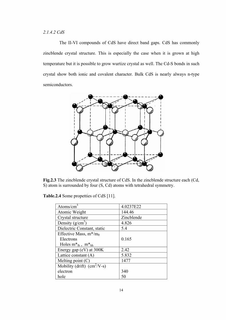
2.1.4.2 CdS
The II-VI compounds of CdS have direct band gaps. CdS has commonly
zincblende crystal structure. This is especially the case when it is grown at high
temperature but it is possible to grow wurtize crystal as well. The Cd-S bonds in such
crystal show both ionic and covalent character. Bulk CdS is nearly always n-type
semiconductors.
Fig.2.3 The zincblende crystal structure of CdS. In the zincblende structure each (Cd, S) atom is surrounded by four (S, Cd) atoms with tetrahedral symmetry.
Table.2.4 Some propetties of CdS [11].
Atoms/cm3 4.0237E22 Atomic Weight 144.46 Crystal structure Zincblende Density (g/cm3) 4.826 Dielectric Constant, static 5.4 Effective Mass, m*/m0 Electrons Holes m*lh , m*hh
0.165
Energy gap (eV) at 300K 2.42 Lattice constant (A) 5.832 Melting point (C) 1477 Mobility (drift) (cm2/V-s) electron hole
340 50

15
2.1.4.3 Crystal and Band Structure of GaSe
The covalently bounded layers of the III-VI compound GaSe contain four
monatomic sheets in the order Se-Ga-Ga-Se. Each single layer is hexagonal and the
c-axis is perpendicular to the layer plane. Atomic configuration of a GaSe layered
semiconductor as follows:
(a) (b)
Fig.2.4 (a) Atomic confg. of GaSe. The open and the full circles represent Se atoms, Ga atoms, respectively [12]. (b) Perspective and top views of a unit of GaSe [13].
Depending on the period of stacking sequences there are four modifications:
ε ,β ,γ and δ. [14]. The ε and β modifications are 2H hexagonal type and γ and δ are
3R trigonal type [15].
The layer compounds consist of sheets which stick to each other to form a
three dimensional crystal. The thickness of sheets is about a few atoms. The bonding
between the atoms of a single layer is covalent and each layer forms a self contained
crystalline unit. Bondings among different layers are formed by weaker forces such
as Van der Waals with some ionic or coulomb contributions. Since there exists
highly asymmetric charge distribution surrounding the atoms, the combination of
strong and weak bands in the structure of the layer compounds result in anisotropic
[15, 17, 18].

16
Fig.2.5 Polytype of GaSe. Crystallographic structures of the ε, β and γ polytypes of GaSe-like compounds. The unit cells are represented by the broken lines. They are hexagonal for the ε, β and rhombohedrical for the γ one [16].
The electronic band structure of GaSe, calculated by the empirical
pseudopotential method [14, 19, 20] shows the existence of a low-lying indirect
minimum of conduction band (CB) at the M point of Brillouin zone which is lower
than the direct one at the Γ point and they located the top of the valance band (VB) at
the center of the Brillouin zone. Optical transition between the VB and the direct and
the indirect minima in the CB are allowed with various strengths depending on the
polarization of the light. While the indirect gap energy in GaSe is 2.102 eV at 4.2 K
[17], the direct gap energy becomes 2.128 eV at 4.2 K and 2.021eV at 300K.
GaSe is highly transparent in the infrared region between the wavelengths
0.65 – 18 µm. At room temperature its resistivity is 100 ohm-cm, hall coefficient of
about 3000cm3/coloumb, and mobility 30 cm2/V [21].

17
Fig.2.6 Band structure of GaSe.
2.1.5 Intrinsic and Extrinsic Semiconductors
Intrinsic semiconductors:
The aim in semiconductors technology is to first purify the material as much
as possible and then introduce impurities in a controlled way. We call the pure
semiconductors “intrinsic”, and we call the semiconductor “extrinsic’’ after external
interference has changed its inherent properties. In devices extrinsic semiconductors
are mostly used, but it is better to start dealing with the intrinsic semiconductors first.
The intrinsic carrier concentration depends on the parameters of
semiconductors such as the bandgap, temperature and the detail of the bandedge
masses. The conduction and valance band density of states are shown in Fig. (2.6).
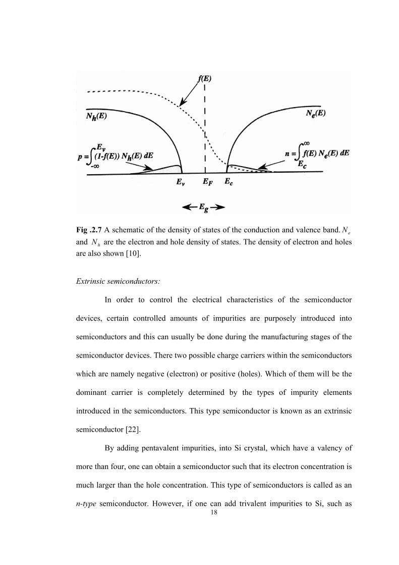
18
Fig .2.7 A schematic of the density of states of the conduction and valence band. eN and hN are the electron and hole density of states. The density of electron and holes are also shown [10].
Extrinsic semiconductors:
In order to control the electrical characteristics of the semiconductor
devices, certain controlled amounts of impurities are purposely introduced into
semiconductors and this can usually be done during the manufacturing stages of the
semiconductor devices. There two possible charge carriers within the semiconductors
which are namely negative (electron) or positive (holes). Which of them will be the
dominant carrier is completely determined by the types of impurity elements
introduced in the semiconductors. This type semiconductor is known as an extrinsic
semiconductor [22].
By adding pentavalent impurities, into Si crystal, which have a valency of
more than four, one can obtain a semiconductor such that its electron concentration is
much larger than the hole concentration. This type of semiconductors is called as an
n-type semiconductor. However, if one can add trivalent impurities to Si, such as

19
boron (B), which have a valency of less than four, there is an excess of holes over
electrons. This kind is called as a p-type semiconductor [23].
Assuming that an element from the Vth column of periodic table such as As,
which have five valence electrons, is substituted for one of the Si atoms within the
crystal. Four out of these five electrons are shared with the four neighboring Si
atoms. Thus when an As atom bonds with four Si atoms, it has eventually one
electron left unbonded. Since this electron can not find a bond to go into, it is left
orbiting around the As atom, as illustrated in below figure [22],
Fig.2.8 As-doped Si crystal. The fifth valance electron of As is orbiting around its side
As can easily give electrons to the conduction band and generate conduction
electrons. These are known as donor atoms. Donor energy levels can be defined as
the energy levels corresponding to the ground state binding energy of the loosely
coupled electrons of the donor atoms. A semiconductor is then described as n-type if
it is doped by donor atoms. Band structure and concentration of charge carriers for an
n-type semiconductor are shown as follows [23]:

20
Fig. 2.9 Energy –band diagram and charge concentration in n-type semiconductors When the impurity is an element from the IIIrd column, the situation
becomes different since, unlike the previous case considered, a forth valence electron
to complete the electron pair binding process is absent and this makes the role of the
impurity atom reversed. The nucleus of impurity atom is treated as a fixed negative
charge and missing electron is replaced by a positive charge, circulating around this
negative core.
Fig. 2.10 B doped Si crystal. Substitution of Si leads to a missing electron which is indeed a hole ( +h ) [22].

21
The addition of an impurity atom from IIIrd column leads to empty energy
states above the top of the valence band so that valence electrons can move and thus
generate additional holes in semiconductor at higher temperatures. The equivalent
band diagram for this case is shown below [23];
Fig.2.11 Energy –band diagram and charge concentration in p-type semiconductors.
The increase in temperature can easily make some of the electron at the top the
valence band excited into these energy states. Then in the valance band empty states
are formed and these are denoted as then equivalent to the generation of holes in the
valence band. The resulting semiconductor is known as p-type since it has excess
positive charge carriers introduced. The impurity atoms of the IIIrd column are
known as acceptor since they simply accept electrons from the valence band. The
corresponding energy level of the impurity atom is then called acceptor energy level
whose band structure and concentration of charge carriers for a p-type semiconductor
are shown in Fig. (2.10).
The carrier concentration in intrinsic and extrinsic semiconductors

22
Concentration of charge carriers can be calculated from the following
integral equation. For electrons, the formula is
( ) ( )∫∞
=cE
e dEENEfn , (2.9)
where cE is the energy of conduction band, Fermi-Dirac function ( )Ef and the
electron density of states ( )ENe in the conduction band are given
( )212
3
2
*
2
22
1)( Ce
e EEm
EN −
=
hπ, (2.10)
( )
−+
=
TkEE
Ef
B
Fexp1
1, (2.11)
and a similar formula for holes can be written as
( )[ ] ( )∫∞−
−=vE
h dEENEfp 1 . (2.12)
Then by putting Eqs. (2.10) and (2.11) into Eq. (2.9) we get an explicit expression
for electrons as
( )
∫∞
+
−−
=
cE
B
F
Ce
TkEE
dEEEmn
1exp
22
1 21
23
2
*
2 hπ. (2.13)
In order to put the carrier density expression into more compact form, let’s define the
following variables
TkEE
B
C−=η ,
TkEE
B
CFF
−=η ,
and we simply get

23
( )∫∞∗
+−
=
0
21
23
22 1exp2
21
F
dmnηηηη
π h, (2.14)
where the integral without the factor in front is called Fermi-Dirac integral,
( ) ( )∫∞
+−=
0
21
21 1exp F
FdFηηηηη ,
and further using the definition of the effective density of states at the
conduction bandedge23
222
=
∗
hπTkm
N BeC , we finally obtain
( )FC FNn ηπ 2
12
= . (2.15)
This expression can be solved numerically. However, a good approximation
can be obtained by assuming Boltzman distribution instead of Fermi-Dirac
distribution. In this case, the probability function for the electron can be
approximated as
( ) ( )( )
−−≈
−
+=
kTEE
kTEE
Ef F
F
expexp1
1 .
This is indeed a good approximation for non-degenerate semiconductors.
With this approach the above integral can be solved analytically and the electron
concentration in Eq. (2.14) simply becomes
( )
−=
TkEE
NnB
CFC exp . (2.16)
In a very similar way one can write the concentration of holes in the valance band
from Eq. (2.12) within the above approximation as

24
( )
−=
TkEE
NpB
FVV exp , (2.17)
where )( **heCV mmNN →= is the effective density of states for the valance
bandedge.
In intrinsic semiconductors the electron concentration is equal to the hole
concentration since each electron in the conduction band leaves a hole in the valance
band. If we multiply the electron and hole concentrations, we have
( )
−
= ∗∗
TkE
mmTkpnB
ghe
B exp2
4 233
2hπ, (2.18)
and considering intrinsic case pn = , which can be denoted as in , we have from the
square root of the equation above
( ) ( )
+−
= ∗∗
TkEE
mmTk
nB
VChe
Bi 2
exp2
2 432
3
2hπ. (2.19)
With the use of Eq. (2.19) Fermi energy in the intrinsic semiconductor iFE is then
obtained
( )
+
+= ∗
∗
e
hB
VCiF m
mTk
EEE ln
43
2. (2.20)
The Fermi level of an intrinsic material lies close to the midgap [10]. Energy
bandgap diagram for intrinsic semiconductors can schematically be depicted as
follows,
Fig. 2.12 Energy bandgap diagram for intrinsic semiconductors with Fermi level.
CB
VB
FiE
CE
VE

25
For the extrinsic semiconductors Fermi level is given in Fig. (2.13).
(a) (b)
Fig.2.13 Energy bandgap diagram for extrinsic semiconductors with Fermi level. (a) for p-type, (b) for n-type. 2.1.6 Defects in semiconductors
It is well known that real crystals are never perfect: they always contain a
considerable density of defects and imperfections that affect their physical, chemical,
mechanical and electronic properties. Having defects in crystals, however, has very
wide implications in various technological processes and phenomena such as
annealing, precipitation, diffusion, sintering, oxidation and others. Defects can
mostly be used as control parameter for getting desired charecteristics in a system.
Therefore, let us talk about the effects of imperfections or crystal defects on a few
important properties of solids. The electrical behavior of semiconductors, for
example, is largely controlled by imperfections inside the crystal and the
development of the transistor and the entire field of solid state device technology has
been originated from this fact.
In real semiconductors, one invariably has some defects that are introduced
due to either thermodynamic considerations or the presence of the impurities during
the crystal growth process. Defects, in general, in crystalline semiconductors can be
characterized as i) point defects, ii) line defects, iii) planar defects, and iv) volume
defects.
CB
VB
FpE
CE
VE
FnECE
VE
26
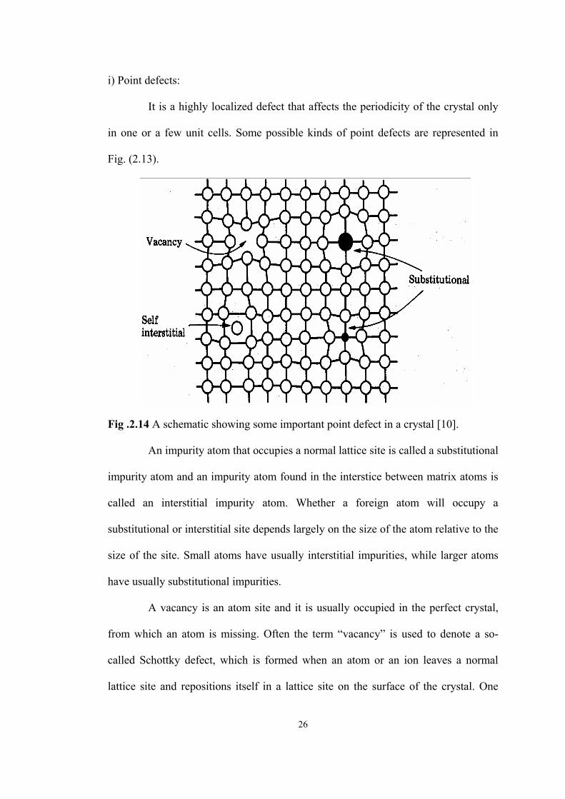
i) Point defects:
It is a highly localized defect that affects the periodicity of the crystal only
in one or a few unit cells. Some possible kinds of point defects are represented in
Fig. (2.13).
Fig .2.14 A schematic showing some important point defect in a crystal [10].
An impurity atom that occupies a normal lattice site is called a substitutional
impurity atom and an impurity atom found in the interstice between matrix atoms is
called an interstitial impurity atom. Whether a foreign atom will occupy a
substitutional or interstitial site depends largely on the size of the atom relative to the
size of the site. Small atoms have usually interstitial impurities, while larger atoms
have usually substitutional impurities.
A vacancy is an atom site and it is usually occupied in the perfect crystal,
from which an atom is missing. Often the term “vacancy” is used to denote a so-
called Schottky defect, which is formed when an atom or an ion leaves a normal
lattice site and repositions itself in a lattice site on the surface of the crystal. One

27
reason for that may be atomic rearrangement in an existing crystal at a high
temperature, which happens when atomic mobility is high because of increased
thermal vibrations. The process of crystallization, appearing as a result of local
disturbances during the growth of new atomic planes on the crystal surface, might be
taken another reason for vacancy formation. Vacancies are point defects of a size
nearly equal to the size of the original (occupied) site; the energy of the formation of
a vacancy is relatively low - usually less than 1 eV.
A vacancy pair defect formed by migration of a cation and an anion to the
surface is usually called a Schottky imperfection, and a vacancy-interstitial pair
defect is referred to as a Frenkel imperfection and it is formed by the result of the
fact that an anion or cation has left its lattice position, which becomes a vacancy, and
has moved to an interstitial position. These two types of imperfections are shown in
Fig. (2.15).
Fig. 2.15 Shottky and Frenkel defects.
28
Other point defects are interstitials in which an atom is sitting in a site in
between the lattice points and impurity atoms which involve a wrong chemical
species in the lattice. The point defects create a local disturbance in the crystal
structure of semiconductors. The effect of this crystal disturbance can be divided into
two categories:
i) The disturbance may create a potential profile which differs from the periodic
potential only over one or a few unit cells. This potential is deep and localized and
the defect is then called a deep level defect.
ii) Unlike the first case, the disturbance may create a long range potential disturbance
which may extend over tens or more unit cells. Such defects are called shallow level
defects.
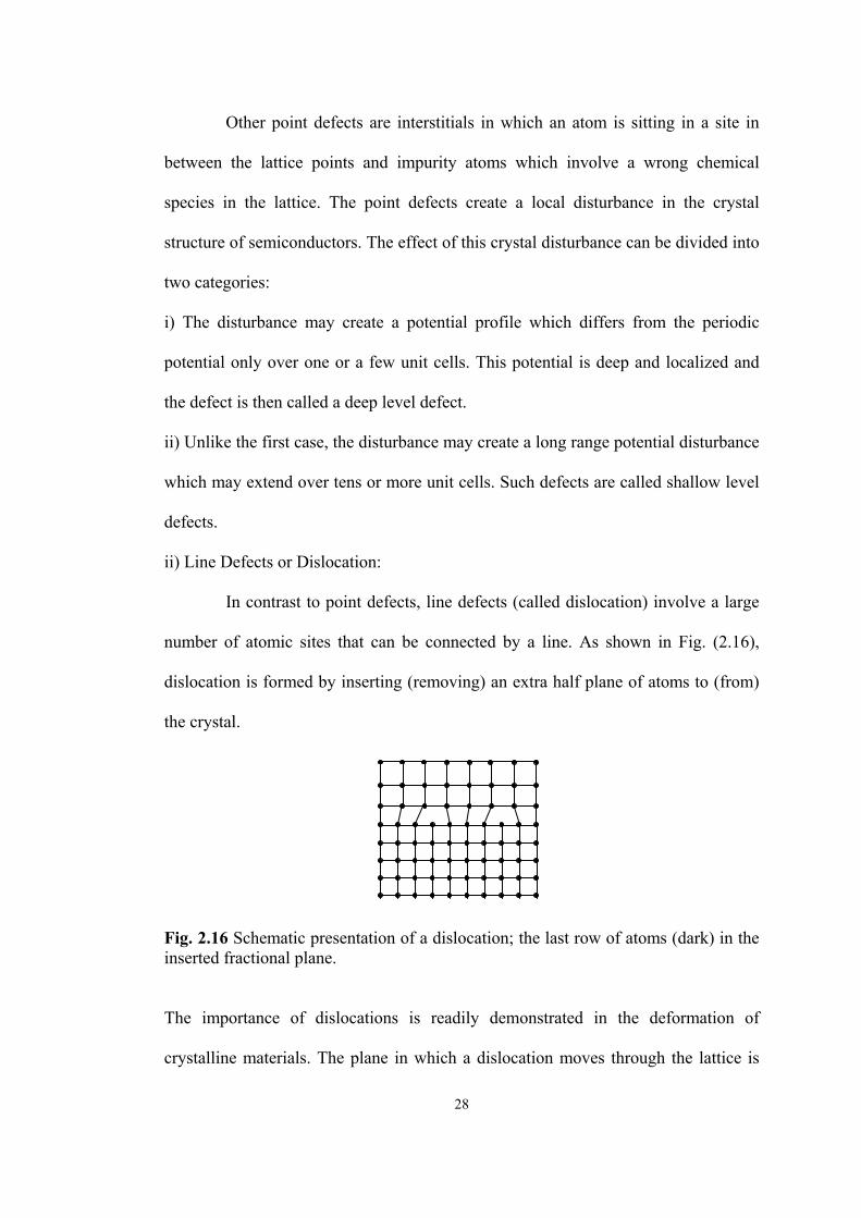
ii) Line Defects or Dislocation:
In contrast to point defects, line defects (called dislocation) involve a large
number of atomic sites that can be connected by a line. As shown in Fig. (2.16),
dislocation is formed by inserting (removing) an extra half plane of atoms to (from)
the crystal.
Fig. 2.16 Schematic presentation of a dislocation; the last row of atoms (dark) in the inserted fractional plane.
The importance of dislocations is readily demonstrated in the deformation of
crystalline materials. The plane in which a dislocation moves through the lattice is
29
called a slip plane. With an applied shear stress the dislocation moves, atomic row by
atomic row, and one part of the crystal is displaced relative to the other. When the
dislocation has passed through the crystal, the portion of the crystal above the slip
plane has shifted one atomic distance relative to the portion below the slip plane.
iii) Planar Defects and Volume Defects
The several different types of interfacial, or planar imperfections, in solids
can be grouped into the following categories:
1. Interfaces between solids and gases, which are called free surfaces;
2. Interfaces between regions where there is a change in the electronic
structure, but no change in the periodicity of atom arrangement, known as domain
boundaries;
3. Interfaces between two crystals or grains of the same phase where there is
an orientation difference in the atom arrangement across the interface; these
interfaces are called grain boundaries;
4. Interfaces between different phases, called phase boundaries, where there
is generally a change of chemical composition and atom arrangement across the
interface.
Grain boundaries are peculiar to crystalline solids, while free surfaces, domain
boundaries and phase boundaries are found in both crystalline and amorphous solids.

30
2.2 OPTICAL PROPERTIES OF SEMICONDUCTORS
2.2.1 Electrons in an electromagnetic field
To describe the interaction of an electron with the electric and magnetic
fields of the electromagnetic field, the energy associated with this interaction is to be
determined. Thus interaction Hamiltonian closely related to this energy is introduced
and is used to describe the dynamics of the scattering electron.
The Hamiltonian for a particle of electric charge e ( 0⟨e for the electron)
bound to a crystal potential ( )rV r is
( )rVm
pH rr
+=2
2
0 . (2.21)
When the electron is subject to electromagnetic field the classical Hamiltonian H0 is
modified as
( )rVeAcep
mH rrr
++
−= φ
2
21 , (2.22)
Where φ and Ar
are the scalar and vector potentials describing the electric and the
magnetic fields.
Using the x-space representation of pr , ∇rh
i the time dependent Schrödinger equation
is
ψψ Ht
i =∂∂
h , (2.23)
where
( ) ( ) φeAmceA
mceiA
mceirV
mH ++⋅∇+∇⋅++∇−= 2
22
2
222
rrrhrrhrrh (2.24)

31
By using the radiation gauge, 0=⋅∇ Arr
and 0=φ , and assuming weak field
approximation (2
Ar
is negligible), the Hamiltonian becomes
'0 HHH += , (2.25)
where
( )rVm
H rrh+∇−= 2
2
0 2
pAmceH rr
⋅−=' . (2.26)
After defining the interaction Hamiltonian, the first order time dependent
perturbation theory gives us the transition rate (that is, the transition probability per
unit time) from the initial electron state i to a group of final state, represented
by [ ]n , of the form
[ ]( ) ( )∑ −=→n
inni EEVniW ωδπhm
h
22 , (2.27)
where iHnVni'= is the matrix element of the perturbation Hamiltonian and the
minus sign in Dirac-delta function represents photon absorption and the positive one
represents emission case. The Eq. (2.27) is known as Fermi s golden rule.
In order to compute the transition rates for either case, the matrix element
niV needs to be evaluated. To this aim, let us work with a monochromatic field of the
plane wave for
−⋅= trn
cAA ωωε rr
ˆcosˆ2 0 , (2.28)
where ε and n are the linear polarization and propagation direction and A0 is the
strength of the vector potential depending on photon number density. Note that the

32
gauge we used ( )0=⋅∇ Arr
is obviously satisfied by this choice for Ar
, since ε in
perpendicular to n .From the simple trigonometric relation ( )θθθ ii ee −+= 21cos we
reexpress the vector potential as
+=
+⋅−−⋅ tirnc
itirnc
ieeAA
ωωωω
εrrr ˆ)(ˆ)(
0 ˆ , (2.29)
where the absorption and the emission cases are more apparent. The term with tie ω−
factor is responsible for absorption and the term with tie ω factor is responsible for
emission. Then the interaction Hamiltonian from Eq. (2.26) becomes
pAmceH rr
⋅−='
=rn
ci
epAmce r
r ⋅±⋅−
ˆ)(
0 ˆω
ε , (2.30)
where + (-) sign refers to absorption (emission) case. The oscillatory time-dependent
part, tie ω− , is indeed represented in the argument of Dirac-delta function in Eq. (2.27).
Before dealing with the matrix element niV for the above perturbation 'H , it
is better to express the strength of the vector potential, 0A , in terms of photon number
density. From classical electromagnetic theory, the energy density of the
electromagnetic wave is
)(81 22 BEu +=π
, (2.31)
where tA
cE
∂∂
−=r
r 1 and ABrrr
×∇= . By using Eq. (2.29) the electric and the magnetic
fields become
)ˆsin(ˆ2 0 wtrnc
Ac
E −⋅=rr ωεω ,

33
)ˆsin(ˆˆ2 0 wtrnc
nAc
B −⋅×−=rr ωεω . (2.32)
Then from Eq. (2.32) and Eq. (2.31) we have
202
2881
21 A
cu ω
π= , (2.33)
where we took time average of the fields. Also if there are pn number of photons, the
energy density for a volume V is
V
nu p ωh= (2.34)
Equating Eq. (2.33) and Eq. (2.34) we get
pnVc
A 2
20
2ωπ h
= (2.35)
Now, let us turn back to the evaluation of the matrix element niV . If we first focus on
the absorption case, the matrix element is
iepAcmenV
rnc
iaani
rr ⋅
⋅−
=ˆ
0 ˆ)(ω
ε , (2.36)
where pa n
VcA 20
2ωπ h
= .
The electric dipole approximation allows us to approximate the exponential
term in Eq. (2.36) as 1 since the wavelength of the radiation field is far longer than
the atomic dimension and thus 1⟨⟨⋅ rnc
rrω is directly obtained. The matrix elements
for both cases are then
ipnAcmeV aa
nir
⋅−
= ε0 ,

34
ipnAcmeV ee
nir
⋅−
= ε0 , (2.37)
where )1(220 += p
a nVc
Aωπ h , since there are 1+pn number of photons in the
emission case which is denoted by the superscript “e”. By inserting the identity
operator, rrrd rr∫= 31 , into the matrix elements we get
n irrprrnrdrdip '''33 ˆˆ rrrrrr⋅=⋅ ∫ ∫ εε
∫ ⋅= )(ˆ)(*3 rprrd inrrr ψεψ , (2.38)
where we have used )(rir irr ψ≡ and )( '' rrrr rrrr
−= δ . Putting all these into the
Eq. (2.27) we have
)()(ˆ)(2)][(2
*32
022
2
ωδψεψπh
rrr
h−−⋅=→ ∑ ∫ inin
aa EErprrdAcm
eniW , (2.39)
and a similar equation is for the emission case. In order to compute the transition rate
we need to know the momentum matrix element. Therefore the transformation rate
for absorption case can be written as
( ) ( ) ( )ωδεωπ
υ hr
h
h−−=→ ∑ in
nc
pa EEpcm
ecn
niW 2
22
2
2
2
.ˆ4
][ . (2.40)
The sum over final states is zero except at resonance fixed by delta function. Thus
this gives us the final state density of states of the form [10]
( ) ( ) ( )32
2/12/3*2h
hh
πω
ωυgr
c
EmN
−= ,
where *rm is the reduced mass of the electron-hole system and gE is the parabolic
band approximation. Finally the expression for transition rate in the case of

35
unpolarized light can be obtained by summing over all possible final polarization
state and dividing over number of polarization states and then we get
( ) ( )ωω
πhcvcv
pa Npcm
enniW 2
42
22
324
][ =→ , (2.41)
and a similar formula can be written for emission case. From this transition rate we
can also compute absorption coefficient for interband transitions. The relation
between them is
pa nvW α= (2.42)
where α is the absorption coefficient, v is the velocity of the wave in the medium,
and pn is the number of photons. This relation can be derived by using continuity
equation for the photon density.
Having obtained the expression for absorption transition rate for direct gap
interband transitions, we can further define absorption coefficient, which might be
more useful than the rate at which photon is absorbed. To relate the absorption
coefficient,α , to the absorption rate, aW , one can consider the continuity equation
for photon density and for photons traveling along χ -direction it is given as in one-
dimension
x
nv
tn
ndtd pp
p ∂∂
+∂∂
= (2.43)
where v is the velocity of the light in the medium, the first term, giving number of
photons absorbed per unit time, represents the absorption rate, and the second one
represents the photon flux due to photon current. In the steady-state case
=∂∂ 0t
from the above relation we have

36
( ) xp enxn α−= 0 , (2.44)
where 0n is the integration constant and α is called the absorption coefficient. Using
Eq. (2.43) and relation ap Wx
n=
∂
∂ we get
a
p
r Wnc
n 1=α , (2.45)
where rn is the index of refraction of the medium. Therefore the absorption
coefficient for interband transitions becomes with the use of Eq. (2.41).
( ) ( )2
12
352
23
2
3224
gcvr EwPwcm
me−= h
hα (2.46)
where we consider the light unpolarized. From Eq. (2.45) we see that the absorption
coefficient α starts as gEw=h , with zero value and initially increases as ( )21
gEw −h .
As energy increases α behaves aswh1 . Note that at higher energies parabolic band
approximation is not valid. In order to evaluateα , we need to know 2cvp which can
be obtained from a knowledge of the conduction band effective mass. The
approximate relation between them can be written from detailed band structure
calculations
g
cv
Ep
mm
2211+≅∗
As a final discussion of this section, we will talk about recombination
time, 0τ . To define 0τ , the recombination rate of an election with a hole at the same
kr
value (direct interband case) is needed. Note that in this we are dealing with
emission rate and then the sum over final states in Eq. (2.40) turns into the sum over

37
all photon states into which such emission could occur. From Eqs. (2.37) and (2.39)
we can write the emission rate as
( ) ( )wpncwcm
enW ifp hrh
hερεπ 2
222
2
ˆ122+= , (2.47)
where aρ is the photon density of states for the polarization ε) and the total photon
density of states is given
( ) 22
2
vwwh
hπ
ρ = . (2.48)
Then if we consider the case 0=pn (vacuum state), the emission rate is called the
spontaneous emission rate and we can define the election-hole recombination time
0τ as
( )01
0 ==
pe nW
τ . (2.49)
The time 0τ represents the time elapsed for an election in a state k to recombine
with a hole in a state with the same k value. If we consider unpolarized light case we
get the expression for 0τ as
12
322
2
02
34
−
= w
mp
vmce cv hh
τ . (2.50)

38
CHAPTER 3
PHOTOLUMINESCENCE SPECTROSCOPY
3.1 LUMINESCENCE SPECTROSCOPY
Luminescence spectroscopy is a powerful tool used for the characterization
of semiconductors, especially those applicable for optoelectronic devices. It is a
nondestructive technique that can yield information on fundamental properties of
semiconductors. It is also sensitive to impurities and defects that affect materials
quality and device performance. A brief introduction of luminescence spectroscopy
and photoluminescence will be presented in this section.
Luminescence is the word for light emission after some energy was
deposited in the material. There are several ways to excite sample to cause
luminescence.
The most common method is Photoluminescence, which describes light
emission stimulated by exposing the material to light - by necessity with a higher
energy than the energy of the luminescence light. Photoluminescence is also called
fluorescence if the emission happens less than about 1 µs after the excitation, and
phosphorescence if it takes long times- up to hours and days - for the emission.
One possible way is to excite the sample by applying an external current,
called as electroluminescence. Electroluminescence is particularly important in the

39
production of optoelectronic devices such as Light Emitting Diods (LED), and
LASERS.
Other ways are Cathodoluminescence, describes excitation by energy-rich
electrons, chemoluminescence provides the necessary energy by chemical reactions
and thermoluminescence describes production of radiation from sample by heating.
3.2 PHOTOLUMINESCENCE
Photoluminescence (PL) is a non-destructive optical technique used for the
characterization, investigation, and detection of point defects or for measuring the
band-gaps of materials. Photoluminescence involves the irradiation of the crystal to
be characterized with photons of energy greater than the band-gap energy of that
material. In the case of a crystal scintillator, the incident photons will create electron-
hole pairs. When these electrons and holes recombine, this recombination energy will
transform partly into non-radiative emission and partly into radiative emission.
Photoluminescence consists of impinging relatively high frequency (hν
> gE ) light onto a material, exciting atomic electrons. Subsequent relaxation may
result in the production of photons that are characteristic of the crystal or defect site
that emits the light. The luminescent signals detected could result from the band to
band recombination, intrinsic crystalline defects (growth defects), dopant impurities
(introduced during growth or ion implantation), or other extrinsic defect levels (as a
result of radiation or thermal effects). When bombarded with photons of energy
greater than the bandgap of the material, an impurity energy level may emit
characteristic photons via several different types of radiative recombination events,
allowing the resultant PL spectra to be used to determine the specific type of

40
semiconductor defect. This interaction provides a highly sensitive, qualitative
measurement of native and extrinsic impurity levels found within the material
bandgap. We can briefly say photoluminescence process includes three main phases
[24]:
1) Excitation: Electrons can absorb energy from external sources, such as
lasers, arc-discharge lamps, and tungsten-halogen bulbs, and be promoted to higher
energy levels. In this process electron-hole pairs are created.
2) Thermalization: Excited pairs relax towards quasi-thermal equilibrium
distributions.
3) Recombination: The energy can subsequently be released, in the form of
a lower energy photon, when the electron falls back to the original ground state. This
process can occur radiatively or non-radiatively.
Fig.3.1 Photoluminescence schematic. (a) An electron absorbs a photon and is promoted from the valence band to the conduction band. (b) The electrons cools down to the bottom of the conduction band. (c) The electron recombines with the hole resulting in the emission of light with energy νh .

41
3.3 RECOMBINATION MECHANISMS
When a semiconductor absorbs a photon of energy greater than the bandgap,
an electron is excited from the valence band into the conduction band leaving behind
a hole. When the electron returns to its original state, it may do so through radiative
(release of a photon) or non-radiative (no photon production) recombination. When
the electron and hole recombine through radiative recombination, a photon is emitted
and the energy of the emitted photon is dependent on the change in energy state of
the electron-crystal system. Indirect bandgap semiconductor, photon emission
requires the aid of a phonon (energy in the form of lattice vibrations) to conserve
momentum within the lattice structure. With the introduction of impurities in
semiconductor material discrete energy levels are formed within the semiconductor’s
forbidden energy gap. Shallow donor levels are defined as levels just below the
conduction band, whereas, shallow acceptor levels are defined as levels just above
the valence band. These donor or acceptor level traps can act as recombination
centers for transitions within the bandgap. By studying the nature of these trap levels,
information about the impurity or defect can be resolved. Figure 1 represents the
energy band diagram of a semiconductor, illustrating the most common radiative and
non- radiative transitions. (The conduction band (EC), occupied by free electrons,
and the valence band (EV), occupied by free holes, are represented in addition to
donor (ED) and acceptor (EA) trapping centers within the forbidden gap. ) These
transitions are band-to-band transition, free-to-bound transition, donor –acceptor pair
transition, excitonic transition, auger transition.

42
Fig.3.2 Most common radiative transition observable with photoluminescence and non-radiative transitions. 3.3.1 Band to Band Transition
The first transitions described here are radiative band-to-band or direct
recombination [Fig.3.2 (a)], which dominate at room temperature and can be used to
estimate the material bandgap energy (Eg). For indirect semiconductors a band-to-
band recombination process is unlikely because the electrons at the bottom of the
conduction band have a nonzero crystal momentum with respect to the holes at the
top of the valence band.
Band -to-band transition contain the recombination of free electrons and
free holes. This transition occurs when an electron falls from its conduction band
state into the empty valence band state associated with the hole.. Band-to-band
transition depends on the density of available electrons and holes and propability
which is proportional to the absorption coefficient. So we can represent the
recombination rate
( )2iennpGRU −=−= α ,
CE
DE
AE
(a) (b) (c) (d) (e) (f) (g)
DL
VE

43
where, α is the recombination constant, ien is the effective intrinsic consentration, n
electron and p hole consentration.
The energy, which is equal to the energy difference between the excited and
ground states, released during the process usually produces a photon and emits light
in a semiconductor having a direct band gap. It is given by the equation:
if EEh −=ν ,
where fE and iE are, respectively, the final and initial state energies. In indirect
semiconductors, band-to-band recombination occurs with phonon contribution and
emitted photon energy is
Ω±−= hEEh ifν ,
Where Ωh is the energy of phonon.
3.3.2 Free to bound transition
At temperature for which TkB is greater than the ionization energy of
shallow impurities, these impurities are ionized, hence band-to-band transition
dominate. At sufficiently low temperautres the thermal energy of carriers becomes
smaller than the ionization energy of the impurities in which case are frozen to the
impurity. For example, in a p-type material containing AN acceptors per unit volume
, holes are trapped at the acceptor if TkB is smaller than AE , where AE is the
ionization energy of the acceptor.
A free electrons can recombine radiatively (and sometimes non-radiatively)
with the holes [Fig.3.2 (c)] trapped on acceptors or holes can recombine with the
electrons trapped on the donors [Fig.3.2 (b)]. Such transition involving free carrier

44
(electron) and a charge (hole) bound to an impurity, are known as free-to-bound
transition. The emitted photon energy is given by
Ag EEh −=ν ,
where AE is the acceptor shallow binding energy. The equation can be written for
the transition, donor to valance band with the energy DE .
If an electron is captured at a donor site, however, it has a high probability
at room temperature of being re-emitted into the conduction band before completing
the remaining steps of the recombination process. A similar statement can be made
for holes captured at acceptor sites. For this reason sites may be likened to extremely
inefficient R-G centers, and the probability of recombination occuring via shallow
levels is usually quite low at room temperature. It should be noted, nevetheless, that
the largest energy step in shallow-level recombination is typically radiative and that
the probability of observing shallow-level process increases with decreasing system
temperature.
3.3.3 Donor-Acceptor Pair Transition
When both donor and acceptor impurities are present in semiconductors,
coulomb interaction between the donors and acceptors modifies the binding energy
in such a way that the transition energy is distance dependent. The DAP (donor
acceptor pair) complex consists of four point charges like an exciton neutral impurity
complex (bound exciton). The donor ion +D and the acceptor ion −A are immobile
point charges while the remaining two charges, an electron and a hole, are mobile.
[Fig.3.2 (d)] shows the usual situation for pair recombination. This process
represented by the reaction

45
−+ ++→+ ADAD oo ωh
The recombination energy of a donor acceptor pair given by
r
eEEErE ADg ε
2
)()( ++−= ,
where gE is the bandgap energy, DE and AE are the binding energy of the donor and
the acceptor and the last term is the coulombing interaction of the donor–acceptor
pair seperated by r.
3.3.4 Exciton Transitions
Free Exciton:
Excitonic recombination , can occur following the generation of an electron-
hole pair (Fig.1.e). Coulombing attaction leads to the formation of an excited state in
which an electron and the hole remain bound to each other in a hydrogen-like state,
reffered to as a free exciton [25].
The energy of the emitted photon is
Xg EEh −=ν
where gE is the bandgap energy of the semiconductor and XE is the Coulomb
energy of the exciton.
Bound Exciton (Exciton-Impurity Interaction):
In reality, many semiconductor materials contain small amounts of natural
defects or impurities forming neutral donors and acceptors. Optically generated free
excitons can interact with those impurities and may become captured by them. They
are then called donor-bound or acceptor-bound excitons depending on wheather the
impurity that the exciton is attached to is a donor or an acceptor.

46
Energy is the fundamental criterion that determines whether or not a free exciton can
be trapped at an impurity. If the total energy of the system is reduced when the free
exciton is in the vicinity of the impurity, then it is energetically favorable for the
exciton to remain near the defect the exciton becomes bound to the impurity via van
der Walls interaction [26] .
These bound exciton can be considered as analog to the hydrogen molecules
2H except for different binding energies. Bound exciton have much smaller binding
energies (usually a few milielectronvolts) because the hole mass is much smaller
than that of the proton and in amedium coulomb interaction is lowered by the square
of the dielectric constant. The common nomenclature is ( )XDo , and ( )XAo , for
neutral-donor bound and neutral-acceptor bound excitons. A photon being emitted
following a bound exciton annihilation has the energy
BXg EEEh −−=ν ,
where BE is the binding energy of the exciton to the defect.
Exciton –Phonon Interaction(Phonon asisted Exciton):
Momentum conservation rules required that only those free excitons can
recombine radiatively which have the same k-vector as the out going photon. Since
the photon momentum is small compared to the momentum of excitons, only
excitons with virtually no kinetic energy (K=0) are allowed to recombine. However,
this condition does not prevent the excitons from having kinetic energy.
Recombination of free excitons with momentum other than the outgoing light can
occur through phonon participation. Phonons provide the necessary momentum to
satisfy the momentum conservation law and thereby reduce restriction on the free

47
exciton momentum allowing of excitons finite K to annihilate. For one-phonon
emission the momemtum, and energy conservation law can be expressed as
phqkK +=
( ) phX hKEh νν −= ,
where the subscript “ph” refers to the phonons and )(KEX is the total energy of free
exciton.
3.4 DEPENDENCE OF PHOTOLUMİNESCENCE ON LASER EXCITATION
POWER
The variation of photoluminescnce intensity, which depends on the power of
the excitation light source can be used to identify the underlineying recombination
process [27]. This is since that the power of the excitation light source is varing. The
general conclusion from the refs. [28,29] is that the luminescence intensity I of the
near bandedge photoluminescence emission lines is proportional to kL , which can be
expressed as
kLI ∝ ,
where L is the power of the exciting laser radiation and 21 ⟨⟨ k for exciton like
transition and 1⟨k for free to bound and donor to acceptor pair ( )00 AD transition.
In order to explain most of the features of near bandedge photoluminescence
emission lines, observed by experiments, [28] et.al proposed a model to predict the
excitation power dependence of these lines which include free-exciton, bound-
exciton, free-to-bound, and donor-acceptor recombination processes. Within
framework of their model, the set of rate equations can be used to describe each of

48
the above recombination mechanisms. By assuming that the electron concentration,
n , in the conduction band and the hole concentration, p , in the valence band are
equal to each other, and further ignoring thermal dissociation of free and bound
excitons, the following coupled differential equations are obtained
( ) 002
ADD enNNNgnaniLdtdn
−−−−= (3.1)
00
112AFEDFEFEnr
FeFE
FE NcnNbnnjLandt
dn−−
+−+=ττ
(3.2)
DXnrDXDX
DFEDX nNbn
dtdn
+−=ττ
110 (3.3)
AXnrAXAX
AFEAX nNcn
dtdn
+−=ττ
110 (3.4)
( )
00
000
0
11
)(
ADAXnrAXAX
AFEAAAAA
NdNn
NcnLNNinNNhdt
dn
−
++
−−+−=
ττ
(3.5)
nfNNdNn
NbnLNknNNgdt
dn
DADDXnrDXDX
DFEDDDD
000
000
0
11
)(
−−
++
−+−=
ττ
(3.6)
In equation (1) - (6) DN and AN concentration of donors and acceptors, 0D
N and
0AN are the concentration of neutral donors and acceptors, FEτ and nr
FEτ are the
radiative and nonradiative lifetimes of donor and acceptor free excitons, and nrDXτ ,
DXτ , AXτ , nrAXτ are clear now on. FEn , DXn and AXn are the concentrations of free
and bound excitons, respectively, and L is the laser intensity. The

49
coefficients a ,b ,….., l are the transition rates of certain recombination processes as
explained in the beginning of this chapter. When we consider the steady state form of
the above differential equations, we are left with a set of algebraic equations and the
luminescence intensities of free and bound excitons, denoted as FEI , XD
I 0 , XA
I 0 , are
deduced through the Eqs. (3.2), (3.3) and (3.4) of the forms
2nnIFEFE
FEFE τ
βτ
== , (3.7)
2
1
0
0 nbNnI
nrDX
DX
D
DX
DXXD
ττβ
τ +== ,
2
1
0
0 nbNnI
nrAX
AX
A
AX
AXXA
ττβ
τ +== , (3.8)
where
00
11ADnr
FEFE
cNbN
a
++
+
=
ττ
β (3.9)
When 0DN and 0A
N are constant the Eqs. (3.1)-(3.4) is enough and Eq.
(3.1) allows us to express the electron concentration n in as a function of L in the
steady state case of the form
LNNgeN
inDDA )( 00 −+
= (3.10)
Then eliminating all n terms from the Eqs. (3.7), (3.8) and (3.9), they read as
22
2
)]([ 00
LNNgeN
iIDDAFE
FE −+=τβ

50
22
2
)]([1 00
0
0 LNNgeN
ibNI
DDAnrDX
DX
DXD −++=
ττβ
22
2
)]([1 00
0
0 LNNgeN
icNI
DDAnrAX
AX
AXA −++=
ττβ
(3.11)
Where the dependence for the free-exciton and bound-exciton intensities on L is
quadratic. Note that for the free-to-bound transitions there is a linear relationship
between the free-to-bound transition intensities and L , which can be deduced by
assuming that the intensity of free-to-donor (acceptor) transitions are proportional
product of both the electron concentration and the concentration of donor (acceptor).
3.5 TEMPERATURE DEPENDENCE OF PHOTOLUMINESCENCE
In this section we want to briefly discuss the effect of the temperature both
on the fundamental gap energy, gE , and on the variation of emission intensity. As we
noted before the temperature dependency of gE can be in generally described by the
empirical formula in Eq. (2.3) as of the form
( ) ( )β
α+
−=T
TETE gg
2
0 , (2.3)
where )0(gE is the bandgap energy at 0 K, α and β are constants. Furthermore,
variation in gE in semiconductors is usually explained by two factors. The first
factor is electron-phonon interaction, and the second one is the thermal expansion of
crystal lattice. The temperature dependent interaction potential describing electron-
phonon couplings can indeed give the major contribution to shift in relative position
of the conduction and the valance bands. These interaction leads to a decrease in gE

51
as the temperature increasing. This behavior can be understood from the above
empirical formula for high temperature values. As T becomes high, the second term
in the Eq. (2.3) behaves as Tα− , resulting in a decrease in gE with respect to its
value at 0 K.
The second factor may lead to either decrease or increase in gE with
temperature. However, it has smaller contributions to ( )TEg than that came from
electron-phonon interaction. Theoretical calculations show that the effect is linear
with T at high temperature unlike the case at lower temperature where α and β have
non-linear T dependency. This means that at low T the dependency is automatically
nonlinear.
The temperature dependence of photoluminescence is often used to probe
the energy levels involved in certain transitions. In order to achieve this aim, we need
to express the variation of emission intensity with temperature which can be
formulated as
( ) ( )
−+
=
kTE
A
ITIaexp1
0 (3.12)
where A is a constant, k is Boltzmann’s constant, and aE is the thermal activation
energy of the transition. For temperature large enough that the following condition is
satisfied,
1exp ⟩⟩
−
kTE
A a ,
the Eq. (3.12) takes the form
( )
−∝
kTE
TI aexp .

52
Therefore, the value of aE can easily be deduced from the slope of the plot of
( )ILog versus kT/1 . The significance of aE comes from the fact that with the use of
it one can determine the energy levels inside the bandgap of semiconductor, which is
the ultimate point to be reached.
3.6 SETUP OF PL
The basic equipment setup needed to perform conventional
photoluminescence consists of three main parts: (1) a light source to provide above-
or below-band-gap excitation; (2) a dewar to maintain the samples at low
temperatures while allowing optical access to the sample surface; and (3) a detection
system to collect and analyze the photons which are emitted from the sample.
A diagram describing the experimental PL set-up is presented in Fig (2.4.3).
Each sample was mounted to a cold finger and placed into a liquid helium-cooled
cryostat that was cooled to the sample temperature variation from 15 K to 300K. The
temperature of the sample was monitored using a Lake Shore 330 Temperature
controller within an accuracy of 5.0± K. The measured luminescence was generated
by 337.1 nm, 2N Laser system operating at average power of 7 mW. The
luminescence collection and detection equipments consists a pair of lenses, mirror,
monochromator, Charge-Coupling-Devices (CCD), and computer (PC). The
excitation pulsed was directed to the sample using mirror, Oriel 17960. The
luminescence emitted was focused by two convex lenses onto the entrance slit of
Oriel model 77700a TMMS257 monochromator and spectrograph. The signal was
spectrally resolved with monochromator. The monochromator is equipped four (4)
grating with 1200 lines/mm- blaze wavelength 350 nm, 300 lines/mm-blaze.

Fig.
3.3
The
sche
mat
ic re
pres
enta
tion
of P
hoto
lum
ines
cenc
e se
t-up.
Exci
tatio
n So
urce
Mirr
or
Vac
uum
Met
er
MC
con
trol w
ith R
S232
Pu
mp
Lens
C
ryog
enic
sy
stem
PC
Sam
ple
Tem
pera
ture
C
ontro
ller
Mon
ochr
omat
or
CC
D
Cam
era
N2 L
aser
, 337
.1nm
53
54
wavelength 400 nm, 150 lines/mm-blaze wavelength 4000 nm, 75 lines/mm-blaze
wavelength 8000 nm. The model 77721 fixed slit housing was used with mounting of
Oriel 1.5 inch (47mm) series. The slit height is 15 mm. The micrometer drive is
metric and a mµ10 movement of the micrometer spindle corresponds to mµ10
change in slit width. Slit width usually sets a limit on the resolution of spectrum, in
our cases it was 1 mm for GaSe, and 35 micron for CdS. The control of the
monochromator was done through RS232 port of the computer by using programs
written in LABVIEW. The Hamamatsu C7041 (S7031-1008 series with 2561044×
number of pixel) multichannel detector was used to detect the PL signals. The C7041
are high sensivity multichannel detector heads developed for use with back-timed
FFT-CCD area image sensors that offer high UV sensitivity and quantum efficiency
and it is designed for a thermoelectrically cooled CCD image sensor for detection at
even lower light levels. The spectra were recorded using a conventional PC
equipped with a SCSI card for the CCD camera. Data acquisition was performed by
using a special computer program provided by the manufacturer.
3.7 EXPERIMENTAL TECHNIQUES USED IN PHOTOLUMINESCENCE
EXPERIMENTS
In the experiments all samples were prepared almost parallel to the crystal
layer. The samples were loaded onto the cold-finger holder, represented Fig. (3.4),
of the closed-cycle cryostat. The PL was observed from the laser-illuminated face of
the samples. All PL spectra were recorded when the system temperature was stabilize
around desired value, which usually requires approximately 15-20 minutes. Some PL


56
CHAPTER 4
PHOTOLUMINESCENCE PROPERTIES OF COMPOUND
SEMICONDUCTORS CdS AND GaSe
4.1 INTRODUCTION
Light emission from compound semiconductors has been an important
phenomenon due to its technological applications. Most of the optoelectronic
components such as light emitter or photodetectors are being fabricated on
compound semiconductors having a direct bandgap with a high emission probability.
Light emission from a semiconductor is a result of transition of a charge carrier from
a higher energy state to a lower state. Usually an electron in the conduction band
makes a transition from conduction band to valence band and recombines with a
hole. This transition takes place effectively only when the semiconductor has a direct
bandgap. Photoluminescence properties of compound semiconductors have thus been
subject of many investigations. Understanding PL spectra of semiconductors are not
always straightforward even for compound semiconductors with relatively simple
band structure. Difficulties arise from the fact that the light emission can result from
various sources that might not be easily resolved. In this work we have studied PL
properties of compound semiconductors CdS and GaSe which exhibits interesting
features.

57
CdS is a direct bandgap material and has been of interest due to its high
efficiency in the solar cells. It is also known as an efficient light emitter of green
light resulting from the band-to-band transition. Recently, it has attracted a great deal
of attention for the production of nanocrystals for biomedical applications. CdS has a
bandgap of 2.42 eV which corresponds to a light wavelength of 510 nm at 300 K. It
is a good material to study the photoluminescence properties.
GaSe is an interesting compound semiconductor with a layer structure. It has
several different phases with different electro-optical properties. Photoluminescence
properties of GaSe crystal show a series of interesting and complicated features. A
series of PL peaks with energies very close to the bandgap are usually observed.
Understanding these features is still a challenging scientific task. One of the reasons
that make the PL properties of GaSe complicated is that it has both direct and
indirect conduction band edges at closely spaced energy positions in the Brillouin
zone. Some researchers have attributed the observed multiple PL peaks to the
presence of two conduction band edge minimum. Also, the optical anisotropy that
exists in both absorption and emission spectra of GaSe makes the PL analysis even
more complicated. Absorption/emission spectra along the direction of crystal axis
which is perpendicular to the plane of the crystal layers has been found to be
different than that observed in the parallel direction. This behaviour has been
explained by the selection rules resulted from the anisotropy of the crystal. In this
work, we have studied the PL properties of GaSe crystal grown by Bridgman
technique in the Crystal Growth Lab. of Physics Department. The dependence of the
PL peaks on temperature and on the polarization has brought about new evidences on
the band structure and anisotropy of GaSe crystal.

58
4.2 PHOTOLUMINESCENCE PROPERTIES OF CdS The PL spectrum of a commercially available CdS crystal at T = 20 K is
shown in Fig.4.1. A series of PL peaks are identified and labeled as PL1, PL2, PL3,
PL4, PL5, PL6, and PL7. The strongest peak (PL1) observed at 490 nm (2.53 eV)
results from the emission from the free exciton located below the conduction
bandedge. Taking the free exciton binding energy as 0.121 meV, we find the
bandgap energy of CdS to be 2.651 eV at 20 K. This value is in agreement with the
reported values of CdS crystal. Four small green PL peaks seen in the low energy
side of the main FE peak were observable below 70 K. The origin of these peaks is
discussed below. A broad red peak (PL6) centered around 696 nm is visible in all
accessible temperatures. Another peak (PL7) whose peak energy located around
449nm (2.76 eV) is larger than the bandgap value becomes visible in temperature
range of 130 K to 20 K.
450 500 550 600 650 700 750 800 850
Inte
nsity
(arb
.uni
t)
W avelength (nm)
PL1
PL2
PL3
PL4
PL5PL6
T~ 20 K
PL7
Fig.4.1 Photoluminescence spectrum of CdS at T~ 20 K
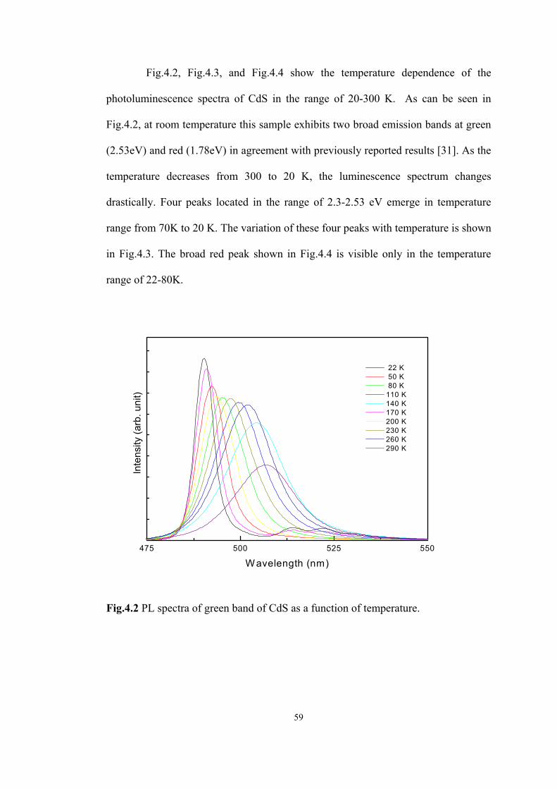
59
Fig.4.2, Fig.4.3, and Fig.4.4 show the temperature dependence of the
photoluminescence spectra of CdS in the range of 20-300 K. As can be seen in
Fig.4.2, at room temperature this sample exhibits two broad emission bands at green
(2.53eV) and red (1.78eV) in agreement with previously reported results [31]. As the
temperature decreases from 300 to 20 K, the luminescence spectrum changes
drastically. Four peaks located in the range of 2.3-2.53 eV emerge in temperature
range from 70K to 20 K. The variation of these four peaks with temperature is shown
in Fig.4.3. The broad red peak shown in Fig.4.4 is visible only in the temperature
range of 22-80K.
475 500 525 550
Inte
nsity
(arb
. uni
t)
W avelength (nm)
22 K 50 K 80 K 110 K 140 K 170 K 200 K 230 K 260 K 290 K
Fig.4.2 PL spectra of green band of CdS as a function of temperature.

60
500 510 520 530 540 550 560
inte
nsity
(arb
. uni
t)
W avelength (nm)
22 K 30 K 40 K 50 K 60 K 70 K 80 K 90 K 100 K
Fig.4.3 PL spectra of the near bandedge transitions of CdS as a function of temperature
650 700 750 800 850 900
22 K 50 K 80 K 110 K 140 K 170 K 200 K 230 K 260 K 290 K
Inte
nsity
(arb
.uni
t)
W avelength (nm )
Fig.4.4 PL spectra of red band for CdS as a function of temperature.

61
The PL spectra of CdS at low temperatures exhibit usually complicated
structure with many emission peaks which are attributed to the transitions involving
both band edge states and localized states of donor and acceptor centers [32]. In the
light of these findings reported previously, the PL emission shown in Fig.4.1 and 4.2
can be explained by a model described schematically in Fig. 4.5 As mentioned above
the main green peak located at 490 nm (2.53 eV) is a result of free exciton emission
across the bandgap of CdS. Four small peak in the low energy side of the FE peak
resulted from the emissions involving localized states. The origin of PL2 peak with
the energy of 2.41 eV is likely to be bound exciton [33] with a binding energy of
0.0079 eV.
Fig.4.5 Optical transition in CdS crystal. The third peak located at 2.37 eV is assumed to be a transition from the
conduction band to the acceptor state and the peak PL4 at 2.33 eV is a transition
from a donor level to the valence band. The last element of the green band, PL5 at

62
2.30 eV is likely to result from the donor-acceptor transition. The origin of the donor
and acceptor states were discussed in the reports published previously [34]. Even
though there might be conflicting results in the literature and the presented evidences
are not convincing enough, some self consisted explanations have been generally
accepted. Donor levels in CdS were attributed to the S vacancies in the CdS crystals
[35, 36, 37]. The acceptor states were attributed to S interstitials [38]. Both of these
descriptions were supported by other experimental evidences [39]. The broad red
band with the peak position at 696 nm was observed by many groups working on
CdS. The origin of this emission is believed to be the transition through the deep
level created by S vacancies. The logarithmic variation of the peak intensity of the
red emission with 1/kT is plotted in Fig.4.6. The slope of the straight part of this plot,
which is the activation energy of this emission, is found to be 0.121 eV. This value is
close to what was obtained in a similar experiment [40]. We can conclude that there
exists another donor level located 0.121 eV below the conduction band edge as
illustrated in Fig. (4.5). The red emission is then found to be a multi step transition
process: in the first step electrons drop to the first donor level located 0.121 eV
below the conduction band edge, and then make a transition to the second deep donor
level at 1.78 eV above the valence band. Finally they fall into the valence band
giving the red emission.

63
0 1 0 0 2 0 0 3 0 0 4 0 0 5 0 0 6 0 0 7 0 0 8 0 0 9 0 0
Inte
nsity
(arb
.uni
t)
1 /kT
L in e a r F it E x p e rim e n t
Fig.4.6 Temperature dependences of red band CdS PL intensity at the emission band
maxima.
4.3 PL SPECTRUM AND BAND STRUCTURE OF GaSe
GaSe is a highly anisotropic semiconductor which consists of layers of
covalently bounded Ga and Se atoms. The layers are bound by weak Van der Walls
forces. The difference in the stacking sequence of the Ga and Se atoms leads to
different polytypes of GaSe identified as β, γ, and ε types. These different polytypes
have slightly different optical properties. It has been suggested that different
polytypes might exists in the same sample [41].
The electronic band structure of GaSe shows the existence of a low lying
indirect gap in GaSe. The indirect minimum of the conduction band at the M point of
the Brillouin zone is lower than the direct bandgap located at Γ point of the zone. It
was found that the indirect band edge is located 25 meV below the direct band edge.
Thus one might argue that GaSe is an indirect bandgap material. However, the

64
difference between direct and indirect band edges is so small that electrons can easily
be transferred between these minimum with a small amount of thermal energy.
Photoluminescence properties of GaSe have been widely studied [14, 42-
52], but there are still discrepancies between experimental findings and their
explanation. This is in part due to the difficulties encountered in growing perfect
single crystals with well known stacking type, and in part due to the difficulties in
understanding the light emission from both direct and indirect nature of the bandgap
of GaSe. In general, the PL spectra of GaSe consist of a series of lines which spread
over a region of about 50 meV lying immediately below the free exciton (FE) line.
These lines were attributed to different mechanisms including bound exciton from
both direct and indirect band edges [44, 45], and the presence of different polytypes
in the same sample [41].
One of the PL spectra of the GaSe samples grown at our laboratory is seen
in Fig. (4.7). This spectrum was obtained with an incidence of 45o with respect to the
crystal axis (case 1 below) angle. The PL peaks are strongly depending on the angle
of incidence of the laser beam due to the anisotropy in the crystal. We discuss the
anisotropy in the next sections. We see that several PL peaks have overlapped. We
have deconvoluted these peaks by using a commercially available computer program.
Deconvoluted peaks are shown in Fig. (4.7). At ~20 K we identify 2 peaks with
energies 2.086 eV, 2.067 eV, respectively. The peak with the highest energy is
obviously corresponding to the FE of the direct band edge. The activation energy
analysis of this exciton peak is given in the next section. From this analysis we find
the binding energy to be 27.1 meV which is consistent with the reported values [45].
This activation energy is almost same are the energy difference between two peaks

65
(~20 eV). The bandgap of the crystal is then found to be 2.113eV. This value is
almost same as the known bandgap of GaSe.
500 550 600 650 700
Fit.Gauss.
* Exp.
Wavelenght (nm)
Inte
nsity
(arb
.uni
t)
Case 1
Fig.4.7 Deconvolution of the photoluminescence spectra into Gaussian lineshapes at ~20 K. (k//c)
Table.3.2.1 Peak energy values of GaSe comparing with the literature.
Case 1 2.084 eV 2.050 eV - For our work at 70K Case 2 2.047 eV 1.976 eV 1.919 eV [42] at 77 K 2.103 eV 2.075 eV 2.037 eV [43,44 ,45] at 77 K 2.098 eV 2.078 eV 2.035 eV [46,47 ,48] 1999,1993 at 77 K 1991
2.098 eV 2.100 eV
2.036 eV 2.030 eV
- -
[49] at 77 K 2.109 eV - -
[50] at 78 K 2.100 eV - -
[51] at 77 K 2.098 eV 2.098 eV 2.029 eV
The energy values of the observed PL peak and their relative distance to FE
peak are shown in Table. (3.2.1). Due to the optical anisotropy the emission is

66
strongly depending on the angle of laser incidence and the detector position. Case 1
and Case 2 correspond two experimental conditions as will be described later. The
peak energy position obtained from these two cases is displayed in the table. Similar,
peak values reported in the literature are also shown for comparison. We see that the
energy values determined from the peak position of the PL spectrum are in
agreement with the values measured by others. From the thermal quenching
experiments presented in the next section, we can conclude that these two PL peaks
(case 1) resulted from the free exciton and bound exciton connected direct band
edge. If they were originating from different polytypes, we would expect no variation
in the relative intensities of the PL peaks.
4.3.1 Temperature dependence of PL spectra
Temperature dependence of PL spectra provides information on the source
of illuminating centers. As described in the previous section, the variation of the
bandgap with temperature is obtained from the temperature variation of the band-to-
band transition. Also the energy position of the illuminating center can be determined
from the activation energy analysis of the PL peaks.
Fig. (4.8) shows the plot of FE peak energy intensity versus 1/kT. The slope
of the line fitted to the straight line part of this graph gives the activation energy of
the FE dissociation. It thus gives the energy difference between FE energy level and
the conduction band edge. We have determined this energy to be 26.4 meV from this
slope as indicated in Fig. (4.8). The bandgap energy is then found by adding this
activation energy to the peak energy of the PL peak. The room temperature bandgap
value is found to be 2.021 eV.

67
0 2 0 0 4 0 0 6 0 0 8 0 0
E x p . F it E x p e rim e n t
Inte
nsity
(arb
.uni
t)
1 /k T
C a s e 1
Fig.4.8 Variation of GaSe PL intensity with reciprocal temperature, at 20 and 300 K.
0 5 0 1 0 0 1 5 0 2 0 0 2 5 0 3 0 01 ,9 8
2 ,0 0
2 ,0 2
2 ,0 4
2 ,0 6
2 ,0 8
2 ,1 0
Ener
gy (e
V)
T e m p e ra tu re (K )
C a se 1
Fig.4.9 Temperature dependence of the peak energy position of the A band.

68
Fig.(4.9) shows the temperature variation of the A band energy in the
temperature range of 20 - 300 K. As expected the bandgap increases with decreasing
temperature with commonly observed characteristics. The A band shifts towards the
red. It is a general practice to explain the bandgap variation by
( ) ( )β
α+
−=TTETE gg
2
0
where ( )0gE , α and β are fitting parameters. These parameters are extracted from
the Fig. (4.9) by making linear fit and the obtained values are 2.11 eV, 3.34x10⁻⁴ and
0.14, respectively.
550 575 600 625 650 675
inte
nsity
(arb
.uni
t)
W avelenght (nm)
22 K 40 K 60 K 80 K 100 K 120 K 140 K 160 K 180 K 200 K 220 K 240 K 260 K 280 K 300 K
A
B
Case1
Fig.4.10 Photoluminescence spectra of undoped p-type GaSe as a function of temperature. k//c. From Fig. (4.10), it can be seen that the intensities of A and B bands
decrease with increasing temperature with the A band quenching much more rapidly
than the B band. The variations in the PL peak intensities of A band and B band with

69
respect to reciprocal temperature are plotted in Fig. (4.8). In the low-temperature
range, the PL intensities of both bands decrease slowly. Above 160 K for A band and
70 K for B band, the rate of intensity decreases for both bands increase significantly
owing to the thermal quenching processes. The activation energies for both bands
were obtained by fitting the high-temperature regions of data the following equation
∆=
TkEIIB
exp0 ,
where I is the PL intensity, 0I is a proportionality constant and Bk is Boltzmann’s
constant. The semilogarithmic plots of the peak intensity as a function of reciprocal
temperature give straight lines in the 70-90 K regions for B band. The slope of these
lines gives the activation energies as 27.1 eV for the B band. We conclude that this
value is the dissociation energy of the bound exciton connected to the direct band
edge.
4.3.2 Optical anisotropy in GaSe
As explained above, GaSe is a highly anisotropic material. The structural
anisotropy results in anisotropy in the electrical and optical properties of GaSe. It has
been reported that both light absorption and light emission properties show
anisotropic behavior. This behaviour was found to result from the dependence of the
transitions on the direction of the electric field vector with respect to the crystal axis.
This dependence is a result of selection rules related to the anisotropic band structure
of GaSe as discussed below. Anisotropy of GaSe was investigated by reflectivity
measurements, where it was found that optical absorption is different for E ⊥ c and
E//c [51]. We have studied the anisotropy in GaSe by measuring the PL emission in
three different experimental configurations as shown in Figure 4.11.

70
Fig.4.11 Experimental conditions for the measurement of anisotropic PL emission. a) Laser beam is directed to the sample surface with an angle of 45o with respect to c-axis. The detector is positioned along the c-axis (k//c). b) Laser beam is directed on the side of the sample. The detector’s position is along the direction perpendicular to the c-axis (c ⊥ k). c) The detector is in the same position as b), but the laser beam falls on the sample with an angle.

71
In the first case (case 1), Fig. (4.11.a), laser is directed to the sample with an angle of
incidence of 45o relative to the c-axis, and the detector is placed at a position where it
measures the light propagating parallel to the c-axis (k//c). The majority of the
detected light has therefore an electric field vector which is perpendicular to the c-
axis, In the configuration (case 2) Fig. (4.11.b), the light beam is directed on to the
crystal from its side so that the wave vector (k) of the light is perpendicular to the c-
axis. The detector faces the crystal side and measures the light having a wave vector
perpendicular to the c-axis (k//c). In the third case (case 3), the detector’s position is
along the direction perpendicular to the c-axis, but the light beam is impinged on the
sample with an arbitrary angle as shown in Fig. (4.11.c). This work represents the
first study that uses the experimental conditions described here.
550 600 650 700
Inte
nsity
(arb
.uni
t)
W avelenght (nm)
k I c Case3k//c Case1k I c Case2
x5
50 K
Fig.4.12 Photoluminescence spectrum of GaSe with respect to k//c and k ⊥ c axis.
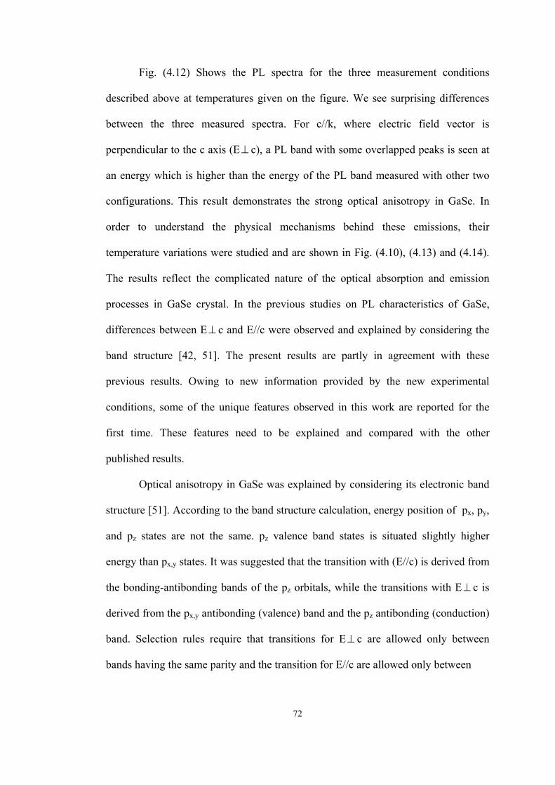
72
Fig. (4.12) Shows the PL spectra for the three measurement conditions
described above at temperatures given on the figure. We see surprising differences
between the three measured spectra. For c//k, where electric field vector is
perpendicular to the c axis (E ⊥ c), a PL band with some overlapped peaks is seen at
an energy which is higher than the energy of the PL band measured with other two
configurations. This result demonstrates the strong optical anisotropy in GaSe. In
order to understand the physical mechanisms behind these emissions, their
temperature variations were studied and are shown in Fig. (4.10), (4.13) and (4.14).
The results reflect the complicated nature of the optical absorption and emission
processes in GaSe crystal. In the previous studies on PL characteristics of GaSe,
differences between E ⊥ c and E//c were observed and explained by considering the
band structure [42, 51]. The present results are partly in agreement with these
previous results. Owing to new information provided by the new experimental
conditions, some of the unique features observed in this work are reported for the
first time. These features need to be explained and compared with the other
published results.
Optical anisotropy in GaSe was explained by considering its electronic band
structure [51]. According to the band structure calculation, energy position of px, py,
and pz states are not the same. pz valence band states is situated slightly higher
energy than px,y states. It was suggested that the transition with (E//c) is derived from
the bonding-antibonding bands of the pz orbitals, while the transitions with E ⊥ c is
derived from the px,y antibonding (valence) band and the pz antibonding (conduction)
band. Selection rules require that transitions for E ⊥ c are allowed only between
bands having the same parity and the transition for E//c are allowed only between

73
550 600 650 700 750
Inte
nsity
(arb
.uni
t)
Wavelength (nm)
46 K 60 K 80 K 100 K 120 K 140 K 160 K 180 K 200 K 220 K 240 K 260 K 280 K 300 K
A B
C
Case3
Fig.4.13 Photoluminescence spectra of GaSe as a function of temperature (k ⊥ c).
5 5 0 5 7 5 6 0 0 6 2 5 6 5 0 6 7 5 7 0 0
Inte
nsity
(arb
.uni
t)
W avelen g th (n m )
2 0 K 5 0 K 8 0 K 1 1 0 K 1 4 0 K 1 7 0 K 2 0 0 K 2 3 0 K 2 6 0 K 2 9 0 K
C ase 2
Fig.4.14 Photoluminescence spectra of GaSe as a function of temperature (k ⊥ c).
74
bands having opposite parity. One can then understand that the high energy peak
observed in the first case (Fig.4.12), where k//c and E ⊥ c, is due to the allowed
transitions between antibonding states of px,y and pz bands. In the second
measurement condition, k ⊥ c and the perpendicular component of electric field is
weak. The transitions with low energy emission dominate the PL spectra in this case
due to smaller energy difference between pz states. An interesting feature of this
second case is that the PL band consists of a single peak which does not appear to be
a combination of several other peaks. Although the asymmetry in the PL band
indicates the existence of different peaks within the main PL band, these peaks are
not resolvable. It is likely that one of the transitions dominates the whole PL
emission and gives the observed spectra. This conclusion is supported by the results
obtained in case 3 in which the laser beam is directed with an angle while the
detector position is kept same. As shown in Fig. (4.12), the emission intensity drops
significantly and different emission peaks are resolvable. This suggests that high
emission intensity in the second case is related to the dominance of the
absorption/emission of the light with k ⊥ c.
It is interesting to study the energy position and the temperature dependence
of the peaks resolved in case 3 (Fig.4.17). In table 3.2, we have displayed the energy
values of the peaks deconvoluted from the band shown in Fig.(4.15) along with the
energy of the peaks observed in case 1 (E ⊥ c). The energy difference between the
peaks is also shown to see the possible energy separation between the illuminating
centers. As discussed above, the observed two peaks are believed to result from the
free and bound exciton transitions in the first case. The energy difference is 0.034 eV
(at 70 K) between the peaks and these values are in close agreement with those

75
published by others. However we see an interesting situation in the third condition.
The energy differences between the peaks are 0.070 eV and 0.056 eV which are
larger than those obtained in the first case.
500 550 600 650 700 750 800
Wavelength (nm)
Inte
nsity
(arb
.uni
t)
Case3
Fig.4.15 Deconvolution of the photoluminescence spectra into Gaussian lineshapes at ~20 K. (k ⊥ c)
A plot of peak intensity vs.1/kT for the two resolved peaks is shown in Fig.
(4.16). In the low temperature range, the PL intensities of both bands decrease
slowly. The activation energies for two bands have been obtained by fitting the high-
temperature regions of the data. The semilog plots of the peak intensity as a function
of the reciprocal temperature give straight lines in the 120-300 K. The slopes of these
lines give the activation energies as 26.4 meV and 24.5 meV for A and B bands,
respectively.

76
50 1 00 1 50 2 00 2 5 0 3 0 0 3 5 0 40 0
A b a n d B b a n d
Inte
nsity
(arb
.uni
t)
1 /kT
C a se 3
Fig.4.16 Variation of GaSe PL intensity with reciprocal temperature (k ⊥ c). Temperature dependence of peak energy for all peaks is plotted in Fig.
(4.17). A and B band peak energies decreases as the temperature increases. Changes
in the peak energy position shifts lower energies as the temperature increases.
50 100 150 200 250 3001.90
1.92
1.94
1.96
1.98
2.00
2.02
2.04
2.06
Ene
rgy
(eV
)
Temperature (K)
A Band B Band
Case3
Fig. 4.17 Temperature dependence of the peak energy position (k ⊥ c).

77
CHAPTER 5
CONCLUSION
Optical properties of semiconductors have been important both from
technological and scientific point of view. Semiconductors emit light in a
controllable manner. One can fabricate devices emitting ordinary light or LASERs in
the visible and infrared region of the spectrum. These devices are used in variety of
applications such as telecommunication, home electronics, industrial and space
applications. In addition to these technological applications, the study of light
emission provides scientific information about the material being studied. As widely
discussed throughout this thesis, basic electronic structure of the material as well as
the defect centers can be revealed by studying the luminescence properties.
Two interesting semiconductors CdS and GaSe have been studied in this
work. Another aim of this work was to study the photoluminescence spectroscopy as
an experimental technique. The experimental set-up for PL spectroscopy has been
improved in the course of this M.Sc study. New experimental approaches have been
adapted to measure the optical anisotropy. The study on CdS and GaSe has been
very exciting due to the interesting features of these materials and also due to the
new insights they brought into the PL spectroscopy.

78
CdS, being II-VI semiconducting compound, has some interesting properties
which make it a beneficial material in optoelectronic devices. The florescent spectra
of CdS exhibit extremely complex behaviour. We investigated the
photoluminescence of CdS as a function of temperature. We observed three bands,
namely the green, the red, and Raman. In our analysis green band of CdS has five
peaks centered in the region 490 – 537 nm with peak energy values 2.53 eV, 2.41
eV, 2.37 eV, 2.33 eV, and 2.30 eV, respectively. In the red band, the peak energy
appears at 696 nm of the value 1.78 eV which overlaps with the prediction of studies
in literature. Raman peak was found at 449 nm with peak energy 2.76 eV in the
temperature range 20 – 130 K. We suggested that, in the green band, PL1 is
interpreted as free exciton, PL2 as bound exciton, PL3 as transition from conduction
band to acceptor state, PL4 as transition from donor level to the valance band, and
the last one (PL5) as the donor-acceptor transition. These peaks except PL1 survive
20 – 70 K. The red band is likely to be the transition through the deep level created
by S vacancies.
For GaSe, photoluminescence spectra were studied as a function of
temperature by considering three cases which are classified according to the angle of
incidence of the laser light and detector position. The layer compound GaSe is
characterized by a strong structural anisotropy with respect to one crystal axis: it
consists of thin tightly bound layers which are stacked on top of each other and the
cohesion between the layers is relatively weak when we compare the cohesion in a
layer. Thus, as expected, different experimental conditions defined above given us
strongly anisotropic energy spectra for the emission. We investigated PL spectra of

79
GaSe within the temperature range 20 - 300 K by means of N2 laser with constant
intensity.
For the case E⊥ c, two broad peaks were observed with energies 2.086 eV,
2.067 eV at around 594 and 600 nm, respectively, in the lowest accessible
temperature (~ 20 K). Both peak energy positions decrease as temperature increases.
Unlike the first peak (A band), the second one (B band) was seen in temperature
range 20 – 90 K but we are still able to barely identify the existence of B band up to
room temperature. We decided that A band is most likely to result in free excitons
and similarly B band is probably originated by bound exciton.
After having discussed the case E⊥ c, we dealt with the E//c case by further
considering two subcases, the k vector parallel to the edge of the crystal (second
case) and making an angle (third case). In the first subcase there exists one peak in
the spectrum with energy 2.027 eV, 612 nm, at 20 K. In the second subcase we
observed three peaks having energies 2.046 eV, 1.975 eV, and 1.911 eV with
centered 606 nm, 627nm, and 649 nm at 70 K, respectively. The behaviour of peak
energy positions shows the characteristic with those in the first case (E⊥ c).
The energy difference between peaks, related to the energy differences among
illuminating centers, is 0.034 eV for the case (E⊥ c), and 0.070 eV and 0.056 eV for
the third case (E//c), which are larger than that of the first case.
The observed optical anisotropy can be understood by considering the band
structure of the GaSe crystal. It was suggested that energy differences in the valence
and conduction band states and the selection rules that govern the absorption results
in the anisotropy observed in the PL emissions.
80
REFERENCES
[1] Linhtowlers in Growth and characterization of semiconductors, ed.by R. A.
Stradling and P.C.Klippstein, Bristol 1990, p. 135.
[2] C.B. Collins, R. O. Carlson and C.J. Gallagher, Phys.Rev.105, 1168, (1957).
[3] L.Ward, “Cadmium Sulfide”, in Handbook of Optical Constant of Solids, Vol.2,
edited by E.D. Palik p.579, (Academic press, Boston, 1991).
[4] S.S. Devlin, “Transport Properties”, in Physics and Chemistry of II-VI
compounds, edited by M. Aven and J.S. Prener, (North-Holland, Amsterdam,
1967).
[5] J.L. Pankove, Optical Processes of Semiconductors (Dover, New York, 1971).
[6] A.G. Kyazym-zade, R. N. Mekhtieva, and A.A. Akhmedov, Sov. Phys.
Semiconductors 25, 840, (1992)
[7] M. Schluter, Nuovo Cimento 13B, 313, (1973)
[8] F. Hulliger, Structural Chemistry of layer type phases (1976)
[9] A. Mercier and J. P. Voitchovsky, J. Phys. Chem. Solids 36, 1411, (1975).
[10] J. Singh, Semiconductors optoelectronic, McGraw-Hill Press, pp.75 (1995).
[11] S. Sze, Physics of semiconductor devices, 2nd ed., JW&S, pp.848-849.
[12] T. Tambo and C. Tatsuyama, Surface Science 222, 343 (1989).
[13] K. Uneo, K. Saiki, A. Koma, Jap. J. Appl. Lett.30, L1352 (1991).
[14] V. Capozzi, Phys Rev B 28, 4260 (1983).
[15] A. Kuhn, A. Chevy, and R. Chevalier, Phys. Stat. Sol.(a) 31, 469 (1975).
81
[16] Y. Depeursinge, Nuova Cimento 64B, 111 (1981).
[17] M. K. Anis, PhD thesis Brighton Polytechnic England (1977).
[18] C. R. Whitehouse , PhD thesis Brighton Polytechnic England (1977).
[19] M. Schluter, Nuovo Cimento 13B , 313 (1973).
[20] Y. Depeursinge, thesis no 297, Ecole polytec. Federela Lausanne, Switzerland
(1978).
[21] N. C. Fernelius, Prog. Crystal Growth and Charact. Of Materials 28, 275-353
(1994).
[22] A. M. Ferendeci, solid state and electron devices, pp.118 (1991)
[23] S. O. Kasap, Principle of Electrical Engineering Material and Devices, pp320
(1997).
[24] Y. Yu, M. Cardona, Fundamentals of Semiconductors, pp.348, springer, Berlin
(1995).
[25] H. K. Schröeder, Semiconductor Material and Device Characterization, New
York, John Willey & Sons, Inc., 624, (1998).
[26] H B. Bebb and E. W. Williams, Semiconductors and Semimetals, Vol.8, (1972).
[27] P. J. Dean, Prog. Cryst. Growth Charact. 5, 89 (1982).
[28] T, Taguchi, J. Shirafuji, and Y. Inuishi, Pyhs. Status Solidi B 68, 727 (1975).
[29] Q.Kim and D.W. Langer, Pyhs. Status Solidi B 122, 263 (1984).
[30] T. Schmit, H Sitter and K. Lischka, J. Cryst. Growth 101, 190 (1990).
[31] M. Agata Solid State Communication 76, 1061 (1990).
[32] D. C. Thomas, and J.J. Hopfıeld, Phys. Rev.128, 2135, (1962).
[33] N. V. Starostin, Opt. Spectros. 75, 770, (1998).
[34] C. H. Henry, R. A. Faulkner and K. Nassau, Phys. Rev. 183, 798, (1969).
82
[35] N. Susa, Jpn. Appl. Phys. 15, 2365 (1976).
[36] B. A. Kulp, Phys. Rev. 125, 1865 (1962).
[37] J. Humemberger, Thin Solid Films 121, 75 (1984).
[38] N. S. Bogdanyuk, Semiconductors 29, 181 (1995).
[39] O. Vigil, J. Vac. Sci. Technol. A, 15, 2282, 1997.
[40] C. Mejia-Garcia et. al., J. Appl. Phys. 86, 3171 (1999).
[41] Y. Fan, T. Schittkowski, M. Bauer, L. Kador, K. R. Allakhverdiev, E. Yu.
Salaev, J. of Luminescence 98, 7, (2002).
[42] J. P. Viotchovsky, A. Mercier , Nuovo Cimento 22 , 273 (1974).
[43] V. Capozzi, M. Montagna , Phys. Rev.B 40, 3182 (1989).
[44] V. Capozzi, Phys. Rev. B 23, 836 (1981).
[45] V. Capozzi, S. Caneppele, M. Montagna, F. Levy, Phys. Stat. Sol. B 129, 247
(1985).
[46] S. Shigetomi, T. Ikari , Philosophical Magazine Letters 799, 575 (1999).
[47] S. Shigetomi, T. Ikari, H. Nakashima, J. Appl. Phys. 74, 4125 (1993).
[48] S. Shigetomi, T. Ikari, H. Nakashima, J. Appl. Phys. 74, 4125 (1993).
[49] S. Shigetomi, T. Ikari, H. Nishimura, J. Appl. Phys. 69, 7936 (1991).
[50] J.L. Brebner, E. Mooser, Phys. Letters 24A, 274 (1967).
[51] W. Y. Liang, J. Phys. C: Solid State Phys. 8, 1763 (1975).
[52] B. G. Tagiev, G. M. Niftiev, and S.A. Abushov, Phys. Stat. Sol.B121, K195
(1984).

83
APPENDIX A
In this appendix we will give some details of momentum matrix element
calculation for an electron moving in an a electromagnetic field discussed in chapter
2.
In the dipole approximation mentioned in chapter 2 the momentum matrix
element for an initial state i to final state n is given by
∫ ∇= )()( '*3 rrrd
ip ilnlin
rrrhr ψψ , (A1)
where 'l and l represent the band indices. If we use the Bloch function form of the
states, we can choose as
nlrki
nl ue nrr⋅=ψ ,
'' ilrki
nl ue irr⋅=ψ , (A2)
where ilu is the cell periodic part of the Bloch state and it has the same periodicity
with background potential seen by the electrons. Then, inpr becomes
')(*3il
rkinl
rkiin ueruerdip in
rrrr rrh
r ⋅⋅−∫ ∇−=
[ ]∫ ∇+−= ⋅⋅⋅−'')(*3il
rkiil
rkiinl
rki ueuekiruerdi iinrrr
hrrrrrr
''*)(3*3
ilnlrkki
ilnli uuerdirdk ni ∇−= ∫∫ ⋅−r
hr
hrrr
ψψ . (A3)
We can use (A3) to determine the selection rules for band to band transition. The
first term in (A3) is zero from the fact that Bloch states are orthogonal for different k

84
values. If we look the integrant in the second term, '*
nlnl uu ∇ is periodic with, say,
period R. Then,
( ) ( )
( ) IIe
uuerdiIIRkki
ilnlRrkki
ni
ni
rrr
vvrv vh
⋅−
+⋅−
=
∇−= ∫ '*3
(A4)
(A4) says that ( ) 0=⋅− Rkk ni
rrr which gives us ni kk
rr= . This means that interband
transitions are vertical. Therefore, the momentum matrix element becomes
inP '*3
klkl uurdi ∫ ∇−= h . (A5)
To calculate momentum matrix element let us consider the near bandedge transitions
from a state in the conduction band to a state in the valance band. Central cell part of
the electronic state can be a pure combination of only s-type states (l=0) or only p-
type states (l=1) for certain special k values. The central cell part of the electrons at
the bottom of the conduction band of direct bandgap materials (k=0) is purely s-type
and let’s denote it as s , i.e., suc =0 . As final states, there are four possible states,
two of which are denoted as heavy hole states (HH) and the others as light hole states
(LH). Let us express the states formed by including both orbital and spin angular
momentum of the electron. If we denote total angular momentum as J = Lr
+ Sr
, they
limits for total principle quantum member j is
sljsl +≤≤− , (A6)
where l and s are the orbital and spin quantum numbers respectively. The possible
values for j of a p-state (l=1) electron (s= 21 ) are
21
23 ,=j , (A7)

85
and for each j there are 2j+1 mj values. The possible states jmj, are 23
23 , , 2
123 , ,
21
23 ,− and 2
323 ,− for 2
3=j , and 21
21 , and 2
121 ,− for 2
1=j . The states 23
23 ,± are
called as HH states, 21
23 ,± as LH states, and 2
121 ,± as split-off states. We will deal
with near bandedge transitions. Thus only HH and LH states are considered in the
valance band. From the theory of addition of angular momenta we can expand the
jmj, states as an expansion of sl msml ,, direct product states of the form
∑=sl mm
slslj msmlmmCmj,
,,),(, , (A8)
where ),( sl mmC is called as Clebsh-Gordon coefficients and they are nonzero if
slj mmm += is satisfied. For 23
23 , == jmj state there is only one combination as
( ) 21
21
21
23
23 ,1,1,1, C=
+= 1,1 , (A9)
where the Clebsh-Gordon coefficient is 1 from normalization and + denotes spin-
up state. Similarly for 23
23 , −== jmj case
−−= 1,1, 23
23 , (A10)
where − represents 21
21 ,− spin-down state. The LH states are
( ) ( ) ++−−= 0,1,01,1,1, 21
21
21
23 CC ,
( ) ( ) −−++−−=− 0,1,01,1,1, 21
21
21
23 CC , (A11)
where we have to determine the Clebsh-Gordon coefficient by using normalization
and orthogonality of states. The normalized states become
[ ]+−−= 0,121,1,3
121
23 ,

86
[ ]−++−=− 0,121,1,3
121
23 . (A12)
Furthermore, the angular past of the states, lml, , can also be expressed in terms of
three independent p-functions which are yx pp , and zp . Since a spherical tensor can
be expressed in terms of components of some vectors, by calling rri
π43 as ip ,
zyxi ,,= we get
[ ]yx pip +−=2
11,1 ,
[ ]yx pip −=−2
11,1 ,
zp=0,1 . (A13)
The non zero elements from the conduction band to the valance band are only
cvzzyyxx psppsppspp === , (A14)
where the equality is clear from symmetry. Consequently, the allowed transitions for
HH states 23
23 ,=HH are
[ ] sppipspHH xyxx +−=2
1
22
1 cvpxx spp −=−= ,
sppspHH yyy 21=
22
1 cvpxx spp == ,
0=spHH z , (A15)
and for 23
23 ,−=HH case
cvx pspHH2
1= ,

87
cvi
y pspHH2
= ,
0=spHH z . (A16)
Similarly we can simply compute the matrix elements of momentum for HH states.
For 21
23 ,=LH case
cvx pspLH6
1−= ,
cvi
y pspLH6
= ,
cvz pspLH6
2= , (A17)
and for 21
23 ,−=LH
cvx pspLH6
1=
cvi
y pspLH6
= ,
cvz pspLH6
2= . (A18)
Since we are dealing with matrix square of the operator pr) ⋅ε , it is better to examine
2. ipn r)ε for different polarizations.
For z-polarized light: z)) =ε .
02=spHH z
232
2
cvz pspLH = . (A19)
For x-polarized light: x)) =ε
221
2
cvx pspHH = ,
261
2
cvx pspLH = . (A20)

88
For y-polarized light: y)) =ε
221
2
cvy pspHH = ,
261
2
cvy pspLH = . (A21)


![Single-photon emitters in GaSe - White Rose University ...eprints.whiterose.ac.uk/115773/1/Single Photon emitters...semiconductors [35] and GaSe [36] as well as for multiple quantum](https://img.pdfslide.us/doc/110x75/60b93ce81d79f27bf66d3171/single-photon-emitters-in-gase-white-rose-university-photon-emitters-semiconductors.jpg)