Embed Size (px)
Citation preview
PHI 5000 Versaprobe-II
Focus X-ray Photo-electron Spectroscopy
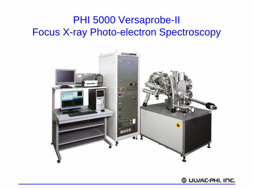
The very basic theory of XPS
XPS theroy
Surface Analysis
Ultra High Vacuum (UHV)
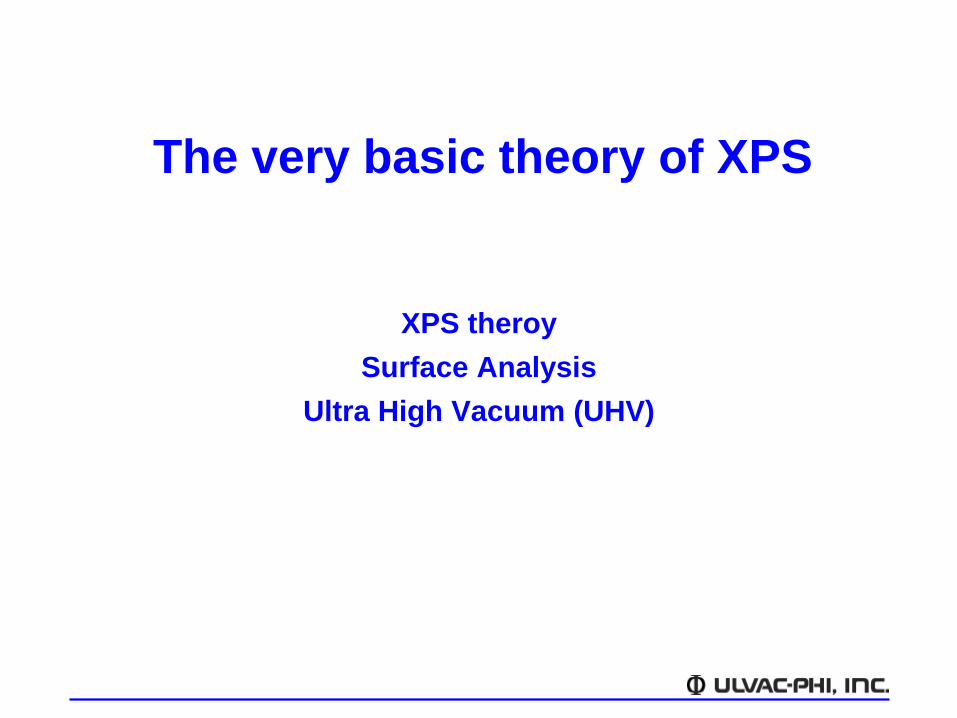
XPS Theory
XPS = X-ray Photo-electron Spectroscopy
X-ray and Photo Electron
Concept of Binding Energy
The XPS equation
hv = KE + BEhv = X-ray energy
KE = Kinetic energy of photo-e
BE = Binding energy
BE = hv - KE
X-ray
Photo-e
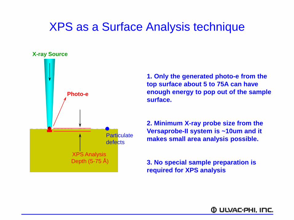
XPS as a Surface Analysis technique
XPS Analysis
Depth (5-75 Å)
Photo-e
1. Only the generated photo-e from the
top surface about 5 to 75A can have
enough energy to pop out of the sample
surface.
2. Minimum X-ray probe size from the
Versaprobe-II system is ~10um and it
makes small area analysis possible.
3. No special sample preparation is
required for XPS analysis
Particulate
defects
X-ray Source
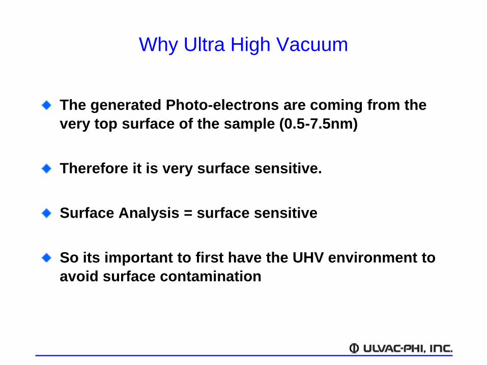
Why Ultra High Vacuum
The generated Photo-electrons are coming from the
very top surface of the sample (0.5-7.5nm)
Therefore it is very surface sensitive.
Surface Analysis = surface sensitive
So its important to first have the UHV environment to
avoid surface contamination
PHI 5000 Versaprobe-II system hardware overview
System component
X-ray Generation
Analyzer Input lens
Hemispherical Spherical Analyzer (HSA)
Multi-Channel Detector (MCD)
Ion gun with floating
Electron Neutralizer
PHI 5000 Versaprobe-II system hardware overview
System component
X-ray Generation
Analyzer Input lens
Hemispherical Spherical Analyzer (HSA)
Multi-Channel Detector (MCD)
Ion gun with floating
Electron Neutralizer
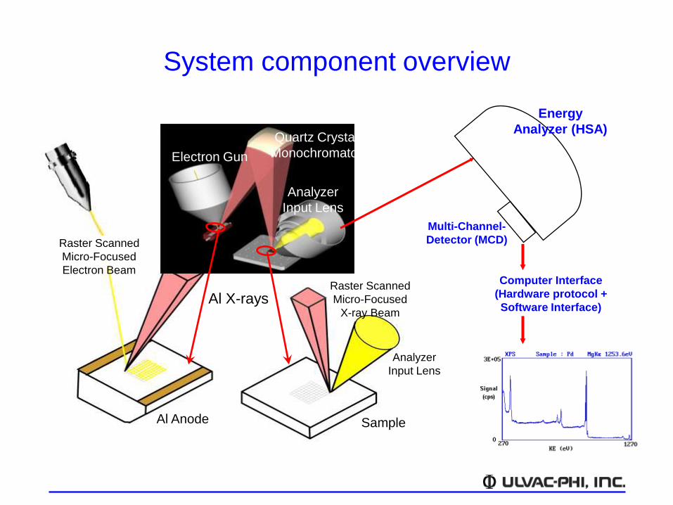
System component overview
Al X-rays
Raster Scanned
Micro-Focused
Electron Beam
Al Anode
Raster Scanned
Micro-Focused
X-ray Beam
Sample
Analyzer
Input Lens
Electron Gun
Quartz Crystal
Monochromator
Analyzer
Input Lens
Energy
Analyzer (HSA)
Multi-Channel-
Detector (MCD)
Computer Interface
(Hardware protocol +
Software Interface)
PHI 5000 Versaprobe-II system hardware overview
System component
X-ray Generation
Analyzer Input lens
Hemispherical Spherical Analyzer (HSA)
Multi-Channel Detector (MCD)
Ion gun with floating
Electron Neutralizer
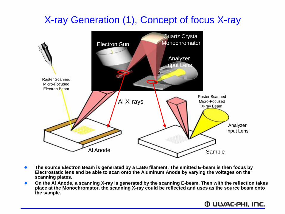
X-ray Generation (1), Concept of focus X-ray
The source Electron Beam is generated by a LaB6 filament. The emitted E-beam is then focus by Electrostatic lens and be able to scan onto the Aluminum Anode by varying the voltages on the scanning plates.
On the Al Anode, a scanning X-ray is generated by the scanning E-beam. Then with the reflection takes place at the Monochromator, the scanning X-ray could be reflected and uses as the source beam onto the sample.
Al X-rays
Raster Scanned
Micro-Focused
Electron Beam
Al Anode
Raster Scanned
Micro-Focused
X-ray Beam
Sample
Analyzer
Input Lens
Electron Gun
Quartz Crystal
Monochromator
Analyzer
Input Lens
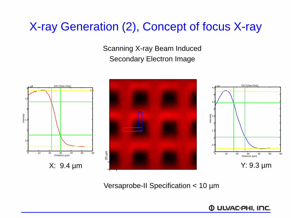
X-ray Generation (2), Concept of focus X-ray
20 µ
m0 10 20 30 40 50 600
0.5
1
1.5
2
2.5
3x 10⁴ SXI (View Only)
Distance (µm)
Inte
nsity
SXI
X: 9.4 µm
0 10 20 30 40 50 600
0.5
1
1.5
2
2.5
3
3.5
4
4.5x 10 SXI (View Only)
Distance (µm)
Inte
nsity
Y: 9.3 µm
Scanning X-ray Beam Induced
Secondary Electron Image
Versaprobe-II Specification < 10 µm
PHI 5000 Versaprobe-II system hardware overview
System component
X-ray Generation
Analyzer Input lens
Hemispherical Spherical Analyzer (HSA)
Multi-Channel Detector (MCD)
Ion gun with floating
Electron Neutralizer
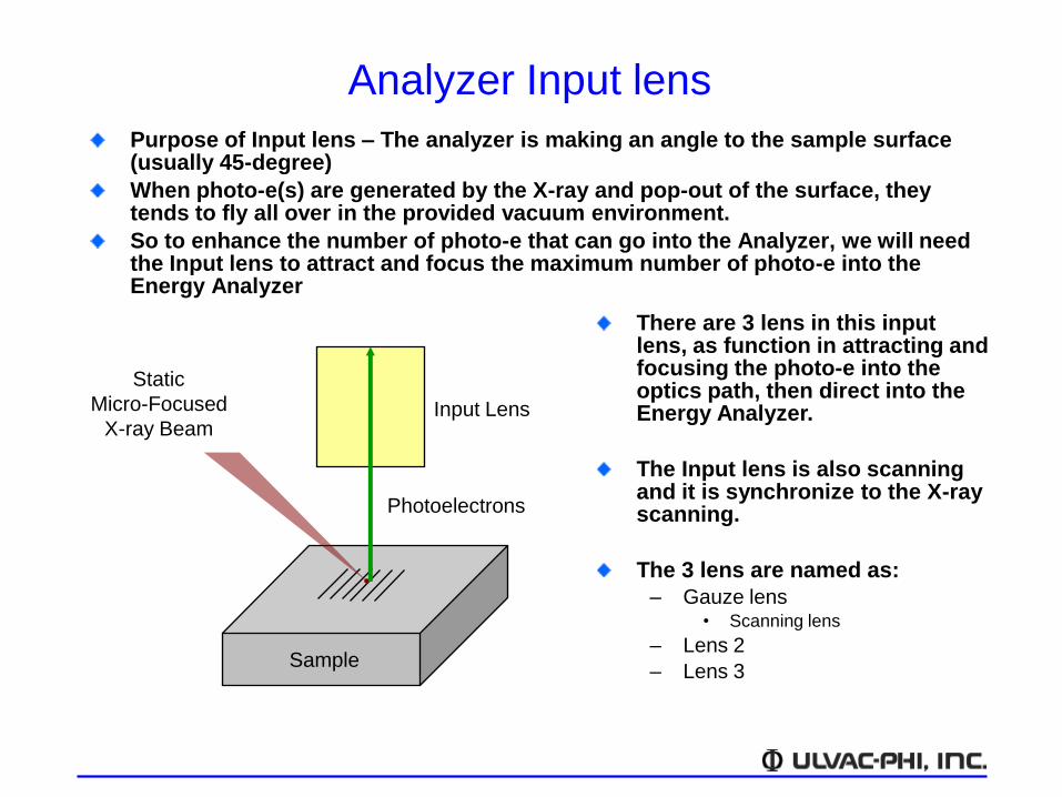
Analyzer Input lens
Purpose of Input lens – The analyzer is making an angle to the sample surface (usually 45-degree)
When photo-e(s) are generated by the X-ray and pop-out of the surface, they tends to fly all over in the provided vacuum environment.
So to enhance the number of photo-e that can go into the Analyzer, we will need the Input lens to attract and focus the maximum number of photo-e into the Energy Analyzer
Input Lens
Photoelectrons
Sample
Static
Micro-Focused
X-ray Beam
There are 3 lens in this input lens, as function in attracting and focusing the photo-e into the optics path, then direct into the Energy Analyzer.
The Input lens is also scanning and it is synchronize to the X-ray scanning.
The 3 lens are named as:
– Gauze lens • Scanning lens
– Lens 2
– Lens 3
PHI 5000 Versaprobe-II system hardware overview
System component
X-ray Generation
Analyzer Input lens
Hemispherical Spherical Analyzer (HSA)
Multi-Channel Detector (MCD)
Ion gun with floating
Electron Neutralizer
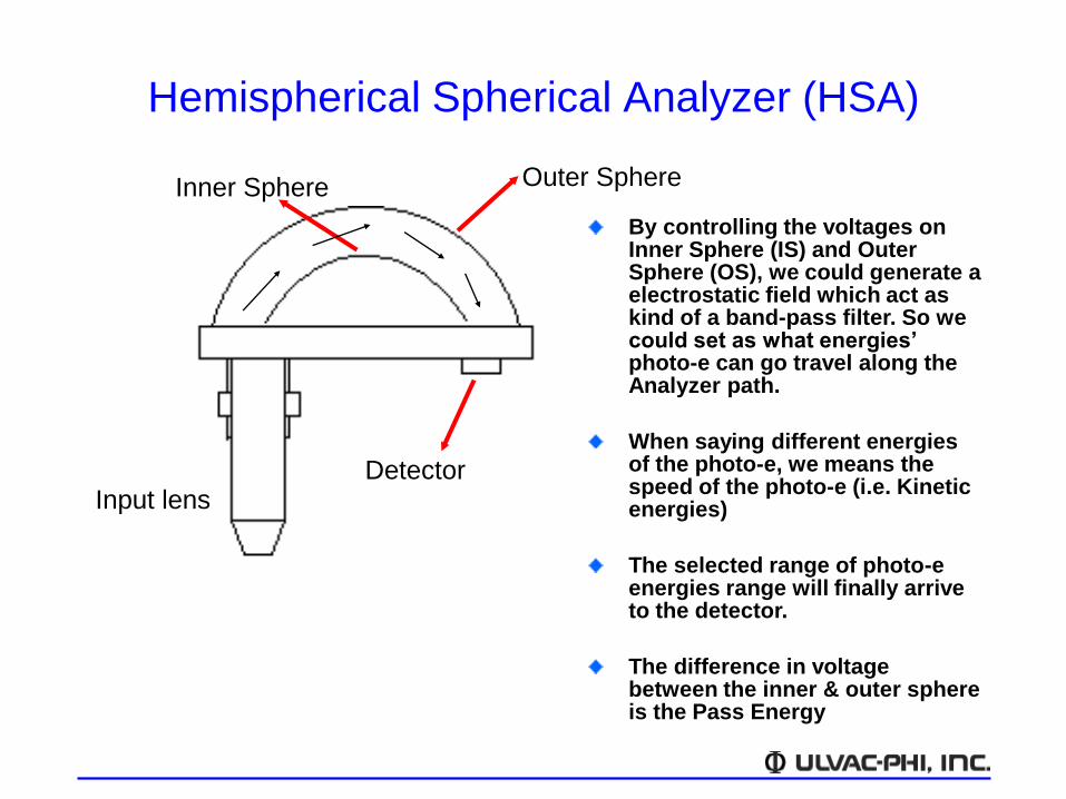
Hemispherical Spherical Analyzer (HSA)
Input lens
Inner Sphere Outer Sphere
By controlling the voltages on Inner Sphere (IS) and Outer Sphere (OS), we could generate a electrostatic field which act as kind of a band-pass filter. So we could set as what energies’ photo-e can go travel along the Analyzer path.
When saying different energies of the photo-e, we means the speed of the photo-e (i.e. Kinetic energies)
The selected range of photo-e energies range will finally arrive to the detector.
The difference in voltage between the inner & outer sphere is the Pass Energy
Detector
PHI 5000 Versaprobe-II system hardware overview
System component
X-ray Generation
Analyzer Input lens
Hemispherical Spherical Analyzer (HSA)
Multi-Channel Detector (MCD)
Ion gun with floating
Electron Neutralizer
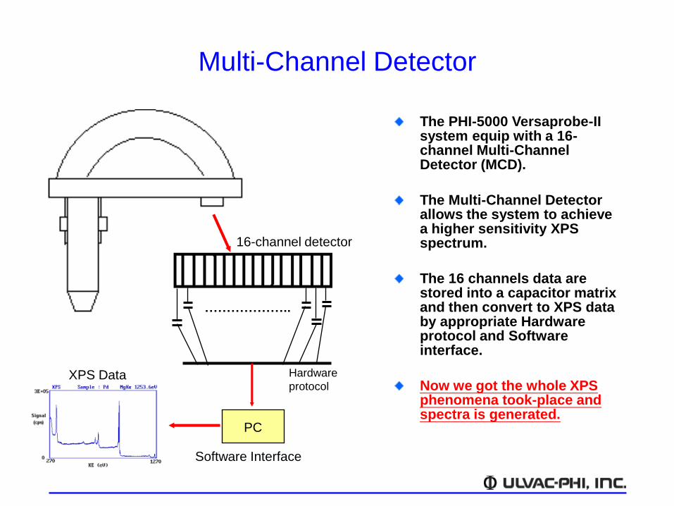
Multi-Channel Detector
16-channel detector
………………..
PC
Hardware
protocol
Software Interface
The PHI-5000 Versaprobe-II system equip with a 16-channel Multi-Channel Detector (MCD).
The Multi-Channel Detector allows the system to achieve a higher sensitivity XPS spectrum.
The 16 channels data are stored into a capacitor matrix and then convert to XPS data by appropriate Hardware protocol and Software interface.
Now we got the whole XPS phenomena took-place and spectra is generated.
XPS Data
PHI 5000 Versaprobe-II system hardware overview
System component
X-ray Generation
Analyzer Input lens
Hemispherical Spherical Analyzer (HSA)
Multi-Channel Detector (MCD)
Ion gun with floating
Electron Neutralizer
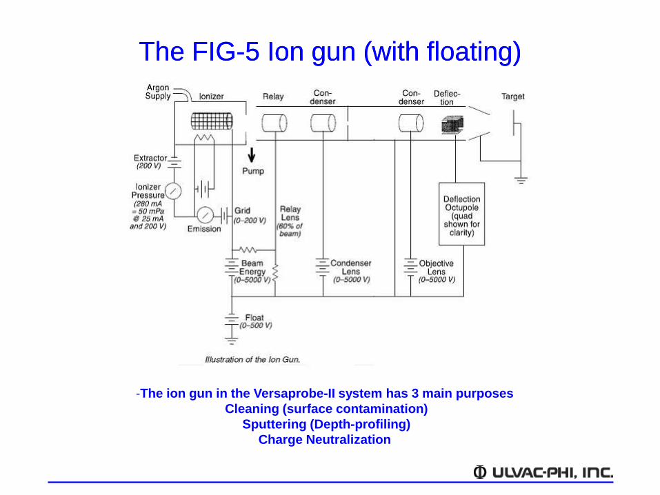
The FIG-5 Ion gun (with floating)The FIG-5 Ion gun (with floating)
-The ion gun in the Versaprobe-II system has 3 main purposes
Cleaning (surface contamination)
Sputtering (Depth-profiling)
Charge Neutralization
PHI 5000 Versaprobe-II system hardware overview
System component
X-ray Generation
Analyzer Input lens
Hemispherical Spherical Analyzer (HSA)
Multi-Channel Detector (MCD)
Ion gun with floating
Electron Neutralizer
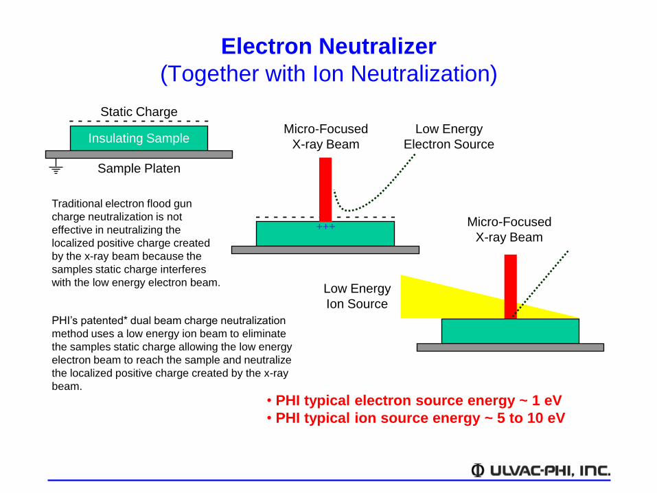
Electron Neutralizer
(Together with Ion Neutralization)
- - - - - - - - - - - - - - - -
- - - - - - - - - - - - - - - -+++
Sample Platen
Insulating Sample
Static Charge
Low Energy
Electron Source
Micro-Focused
X-ray Beam
Micro-Focused
X-ray Beam
Low Energy
Ion Source
Traditional electron flood gun
charge neutralization is not
effective in neutralizing the
localized positive charge created
by the x-ray beam because the
samples static charge interferes
with the low energy electron beam.
PHI’s patented* dual beam charge neutralization
method uses a low energy ion beam to eliminate
the samples static charge allowing the low energy
electron beam to reach the sample and neutralize
the localized positive charge created by the x-ray
beam.
• PHI typical electron source energy ~ 1 eV
• PHI typical ion source energy ~ 5 to 10 eV
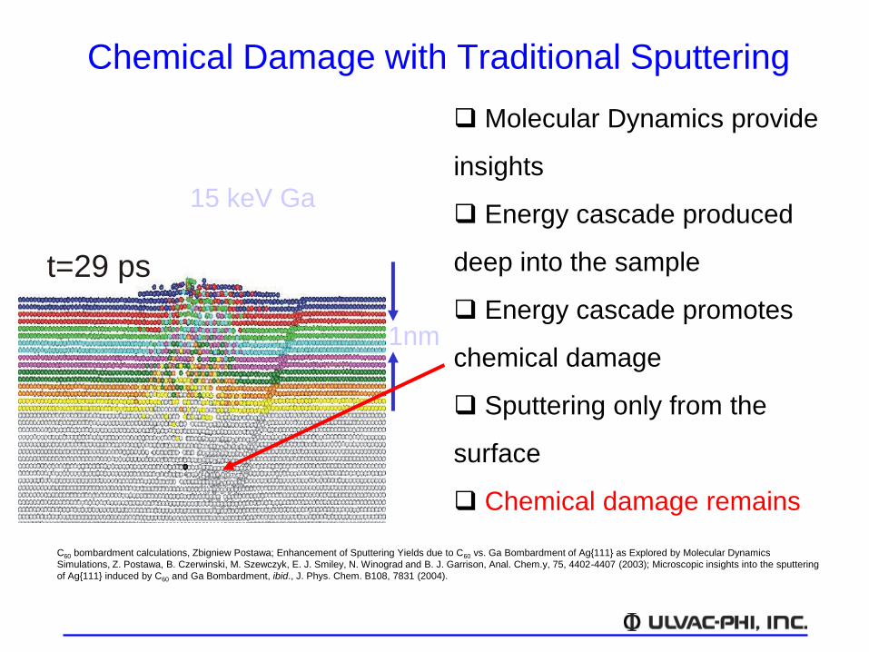
t=29 ps
15 keV Ga
Chemical Damage with Traditional Sputtering
C60 bombardment calculations, Zbigniew Postawa; Enhancement of Sputtering Yields due to C60 vs. Ga Bombardment of Ag{111} as Explored by Molecular Dynamics
Simulations, Z. Postawa, B. Czerwinski, M. Szewczyk, E. J. Smiley, N. Winograd and B. J. Garrison, Anal. Chem.y, 75, 4402-4407 (2003); Microscopic insights into the sputtering
of Ag{111} induced by C60 and Ga Bombardment, ibid., J. Phys. Chem. B108, 7831 (2004).
1nm
Molecular Dynamics provide
insights
Energy cascade produced
deep into the sample
Energy cascade promotes
chemical damage
Sputtering only from the
surface
Chemical damage remains
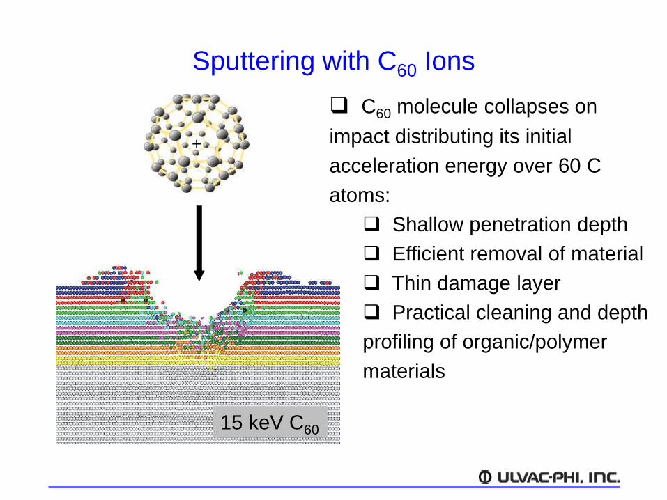
Sputtering with C60 Ions
+
15 keV C60
C60 molecule collapses on
impact distributing its initial
acceleration energy over 60 C
atoms:
Shallow penetration depth
Efficient removal of material
Thin damage layer
Practical cleaning and depth
profiling of organic/polymer
materials
So what can the PHI 5000 Versaprobe-II system do?
Real-life examples…
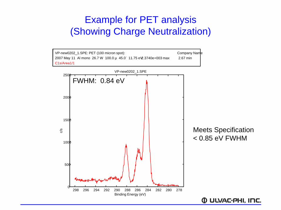
Example for PET analysis
(Showing Charge Neutralization)
VP-new0202_1.SPE: PET (100 micron spot): Company Name
2007 May 11 Al mono 26.7 W 100.0 µ 45.0° 11.75 eV2.3740e+003 max 2.67 min
C1s/Area1/1
FWHM: 0.84 eV
2782802822842862882902922942962980
500
1000
1500
2000
2500VP-new0202_1.SPE
Binding Energy (eV)
c/s Meets Specification
< 0.85 eV FWHM
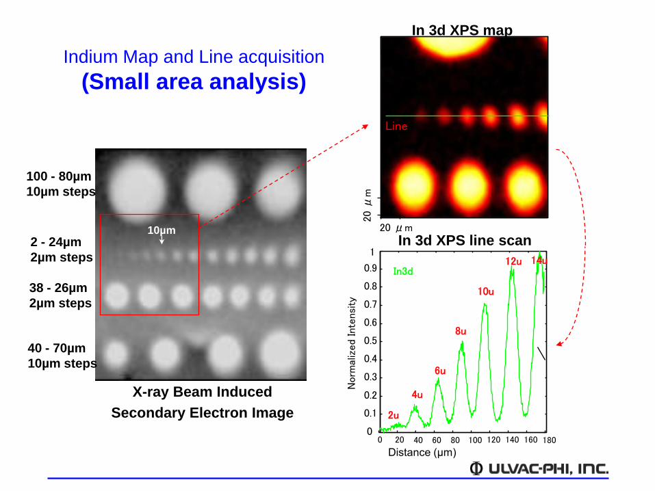
Indium Map and Line acquisition
(Small area analysis)
0 20 40 60 80 100 120 140 160 1800
0.1
0.2
0.3
0.4
0.5
0.6
0.7
0.8
0.9
1
Distance (μm)
Norm
aliz
ed Int
ensi
ty
In3d
4u
6u
8u
10u
12u 14u
2u
100 - 80µm
10µm steps
2 - 24µm
2µm steps
38 - 26µm
2µm steps
40 - 70µm
10µm steps
10µm 20 μm
20 μ
m
In 3d XPS map
Line
X-ray Beam Induced
Secondary Electron Image
In 3d XPS line scan
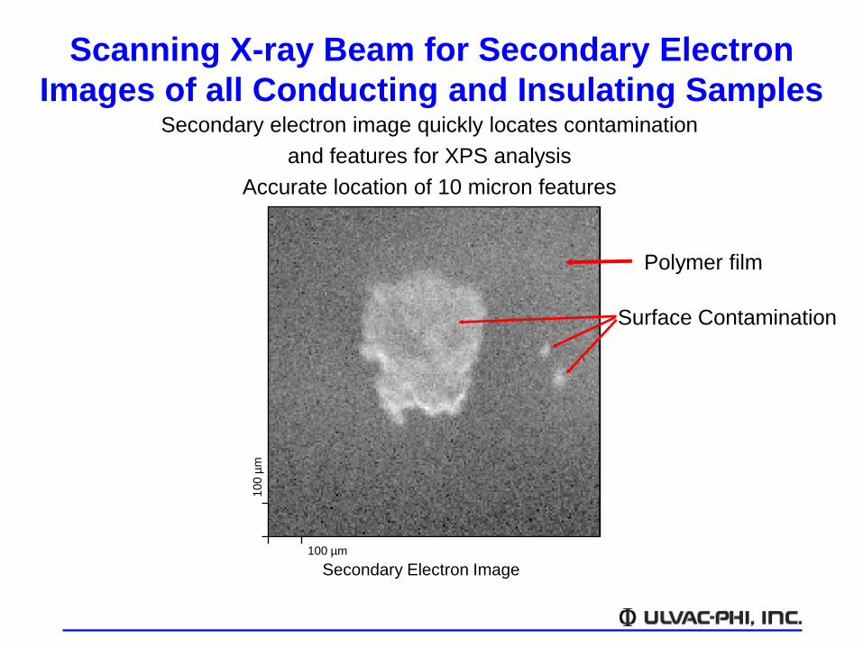
Scanning X-ray Beam for Secondary Electron
Images of all Conducting and Insulating Samples
100 µm
100 µ
m
Secondary electron image quickly locates contamination
and features for XPS analysis
Accurate location of 10 micron features
Polymer film
Surface Contamination
Secondary Electron Image
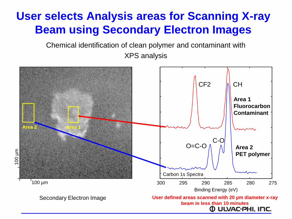
User selects Analysis areas for Scanning X-ray
Beam using Secondary Electron Images
100 µm
10
0 µ
m
Area 2 Area 1
Secondary Electron Image
275280285290295300
Binding Energy (eV)
Carbon 1s Spectra
Area 1
Fluorocarbon
Contaminant
Area 2
PET polymer
CF2 CH
O=C-OC-O
User defined areas scanned with 20 µm diameter x-ray
beam in less than 10 minutes
Chemical identification of clean polymer and contaminant with
XPS analysis
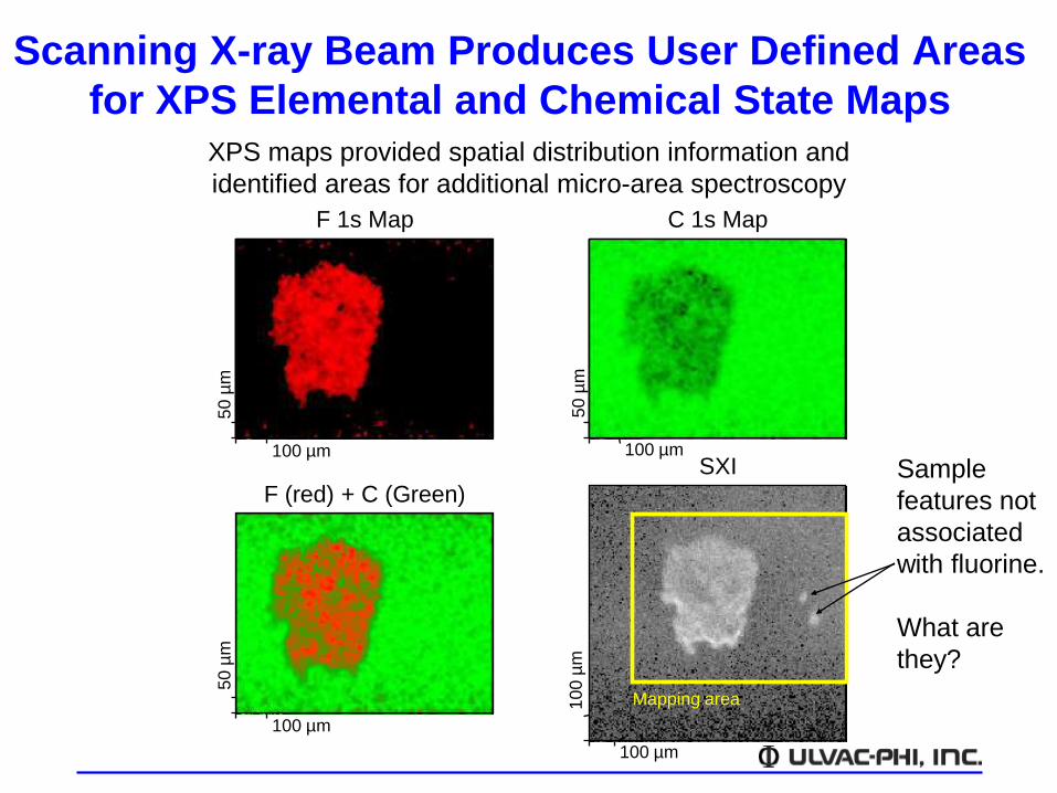
Scanning X-ray Beam Produces User Defined Areas
for XPS Elemental and Chemical State Maps
50
µm
100 µm
F 1s Map
50
µm
100 µm
C 1s Map5
0 µ
m
100 µm
F (red) + C (Green)
100 µm
10
0 µ
m
Mapping area
SXI Sample
features not
associated
with fluorine.
What are
they?
XPS maps provided spatial distribution information and
identified areas for additional micro-area spectroscopy
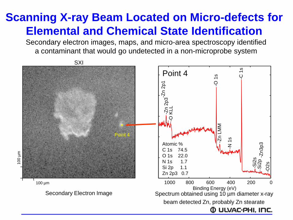
Scanning X-ray Beam Located on Micro-defects for
Elemental and Chemical State Identification
02004006008001000
Binding Energy (eV)
-Zn
2p
1-Z
n 2
p3
-O K
LL
-O 1
s-Z
n L
MM
-N 1
s
-C 1
s
-Si2
s-S
i2p
-Zn3
p3
-O2
s
Atomic %
C 1s 74.5
O 1s 22.0
N 1s 1.7
Si 2p 1.1
Zn 2p3 0.7
100 µm
100 µ
m
Point 4
SXI
Point 4
Spectrum obtained using 10 µm diameter x-ray
beam detected Zn, probably Zn stearate
Secondary electron images, maps, and micro-area spectroscopy identified
a contaminant that would go undetected in a non-microprobe system
Secondary Electron Image
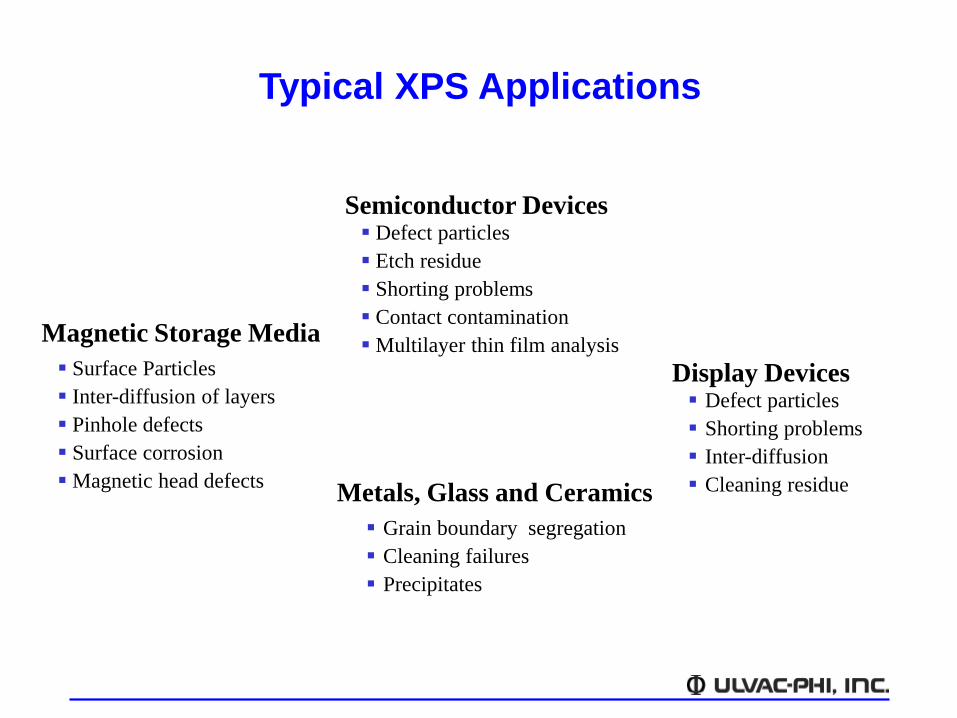
Typical XPS Applications
Semiconductor Devices
Magnetic Storage Media
Display Devices
Metals, Glass and Ceramics
Defect particles
Etch residue
Shorting problems
Contact contamination
Multilayer thin film analysis Surface Particles
Inter-diffusion of layers
Pinhole defects
Surface corrosion
Magnetic head defects
Defect particles
Shorting problems
Inter-diffusion
Cleaning residue
Grain boundary segregation
Cleaning failures
Precipitates

PHI 5000 Versaprobe-II
Focus X-ray Photo-electron Spectroscopy