Embed Size (px)
Citation preview
Characterization of plasma-treated surfaces by X-rayPhotoelectron Spectroscopy (XPS)
Teresa de los Arcos
September 13, 2010
X-Ray photoelectron spectroscopy (XPS) is a technique used to determine the ele-mental composition and chemical state (among other things) of surfaces. The goal of thispractical course is to use XPS in order to gain information about the changes induced ina surface due to di�erent plasma treatments. Due to time constrictions, the samples nec-essary for the execution of this experiment must have been previously prepared in otherplasma-related experiments. At the moment, this experiment can be combined with thefollowing f-Praktika:
• Ober�ächen Modi�kation mit Mikroplasmen (Dr. Volker Schulz von der Gathen)
• 402 Anwendungsorientierte Plasmaphysik (Dr. Marc Böke)
1
1 TheoryX-ray photoelectron spectroscopy (XPS) is an extremely powerful technique for the anal-ysis of the chemical composition and electronic characteristics of surfaces.
The technique is based in the photoelectric e�ect, where electrons are emitted by amaterial after irradiation with photons. The kinetic energy of the emitted electrons canbe related to the energy of the photons by the following formula:
hν = Ekin + Eb + Φ (1)Where hν is the energy of the incoming photon; Ekin is the kinetic energy of the emitted
electron, which we measure; Φ is the work function of the sample (the extra energy thatthe electron needs in order to physically leave the solid); and Eb is the binding energyof the electron in the material, which is what we want to determine. Therefore, if weirradiate the sample with photons of known energy, we can determine the original bindingenergy of the electron by simply measuring the kinetic energy.
Since each atom has its own distribution of core energy levels, it is possible to use XPSto determine the elemental composition of a sample surface (Si, C, O, etc). Furthermore,the precise binding energy position is also strongly in�uenced by the chemical environmentof the atom, and therefore, XPS can be used also to determine quantitatively the precisechemical composition of each element (Si, SiO2, etc.)
Photoelectron spectroscopy is a Ultra-High-Vacuum (UHV) methode, and we willoperate within a pressure range of 10−7− 10−6 Pa. The low pressure is neccesary in orderto:
• avoid scattering of the photoelectrons between the sample surface and the detector,
• avoid arcing between the high voltage components of the electronic,
• keep the sample surface clean.
The mean free path of the photoelectrons within the sample is relatively short. Thismeans that, although we will produce photoelectrons at several microns depth withinthe sample, only those electrons originating from the top few atomic layers will be ableto actually leave the sample without being reabsorbed. This fact makes XPS extremelysurface sensitive, and we will only be able to investigate the chemical composition ofapproximately the �rst 5 nm of the surface. This means that if the sample surface iscovered with a contaminant layer of adsorbed species (for example, from contact with theair), we will always measure this contaminant layer. If this layer is thicker than ∼ 5 nm wewill not be able to see the surface of interest. XPS is therefore a unique surface sensitivetechnique for chemical analysis.
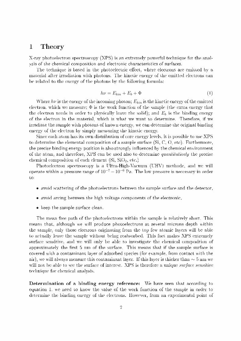
Determination of a binding energy reference: We have seen that according toequation 1, we need to know the value of the work function of the sample in order todetermine the binding energy of the electrons. However, from an experimental point of
2
view, it is very di�cult to determine simultaneously a binding energy reference and thework function of the sample. The solution employed in modern spectrometers is to useas a reference, not the work function of the sample under study, but the work functionof the spectrometer. What we do is to put the sample in good electric contact with thespectrometer, so that the two Fermi levels will be aligned. Our value for binding energyzero will be the position of the Fermi Level of both sample and spectrometer. The problemof the determination of the surface work function is also solved, since we can now use inour formula the known constant value of the work function of the spectrometer. Thecomputer will perform this calculation automatically. We will obtain in our computerscreen already the converted binding energy values of the photoelectrons. You can see anillustration if this in Figure 1.
Efot
Vac Level
Fermi Level
Ebin
EkinE´kin
fspectfsample
Figure 1: Illustration of Fermi-level alignment of a metallic sample and the spectrometer.
In certain cases it is not possible to have a good electric contact between the sample andthe spectrometer. This is going to be the case when the samples are not good conductors.In this case there are two e�ects that we need to take into account: sample charging anda �oating Fermi Level for the sample with respect to the spectrometer.
Sample charging: A non conducting sample does not have su�cient delocalized con-duction band electrons available in order to neutralize the positive holes left behind duringthe photoe�ect. As a result, a positive potential builds near the sample surface, which re-tards the outgoing electrons, making them lose some of their original kinetic energy. This
3
retardation appears in the spectrum as a positive shift towards higher binding energies.This e�ect does not occur in good conducting samples or in narrow gap semiconduc-tors, because at room temperature these systems have enough conduction electrons toneutralize the positive charge at the surface.
The solution to this problem is to neutralize the positive charge externally. In order todo this, we will irradiate the sample simultaneously with a �shower� of low energy electrons(to neutralize the positive charge) and low energy ions (to improve the homogeneity of theneutralization). Failure to compensate the charge in this way results not only in extremeshifts in binding energy positions, but also in deformation of the peak shape.
Fermi Level alignment: A serious problem is the establishment of a Fermi Levelposition, or zero reference position for the energy scala. This problem is inherent to theway in which modern spectrometers perform the measurement, and cannot be solved bythe neutralization procedure described above. As we can see in the Figure 1, in the caseof metallic samples the establishment of a reference energy level is a problem because theFermi levels of sample and spectrometer align themselves automatically. In the case of anon-conducting sample this alignment does not take place, becuase the sample and thespectrometer are not in electrical contact.
In these cases, the best procedure is to establish an arbitrary reference that will serveto �x the scala. In the case of polymer samples, we will do this by �xing the C1s corelevel of C-C bonding at a binding energy of exactly 285.0 eV. In the general case, we willuse the C1s signal corresponding to adventitious carbon (an unde�ned carbon-containinglayer that appears on the surface on every sample exposed to the air due to adsorption ofdi�erent molecules), which we will �x at an arbitrary value of 284.7 eV.
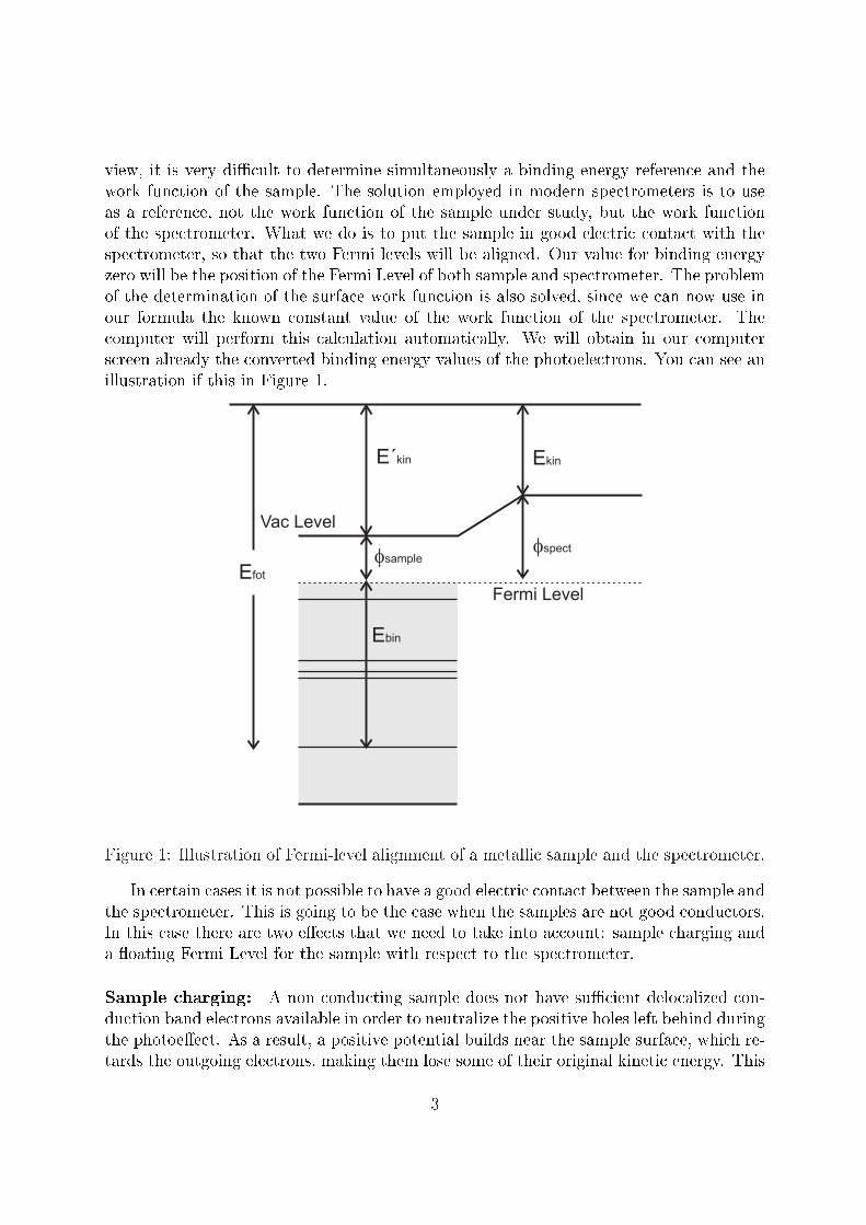
1.1 The spectrometerThe spectrometer that we will use for this experiment is a Versaprobe model from PhysicalElectronics, whose schema we can see in the Figure 2. It is basically divided in three parts:X-ray source, spherical analyzer and detector.
X-ray source: An electron beam with an energy of 15 kV impinges onto an Al anode.There is production of X-ray radiation due to the excitation and radiative relaxation ofinternal Al core levels. This X-ray radiation passes through a monochromator. Finallywe obtain a monochromatized beam of photons with energy of 1486.6 eV, correspondingto the Al Kα transition. The diameter of the X-ray beam is 100 µm.
Spherical Analyzer: The core of the spectrometer is the spherical analyzer, whichperforms electron separation according to their kinetic energy. The analyzer is composedof two concentric half spheres, separated by a thin space. The entrance slit is at oneside, and the detector is located at the other side. The electrons emitted from the samplehave to travel the thin space between the hemispheres in order to reach the detector. Byapplying a potential di�erence between the two hemispheres we create a radial electric
4
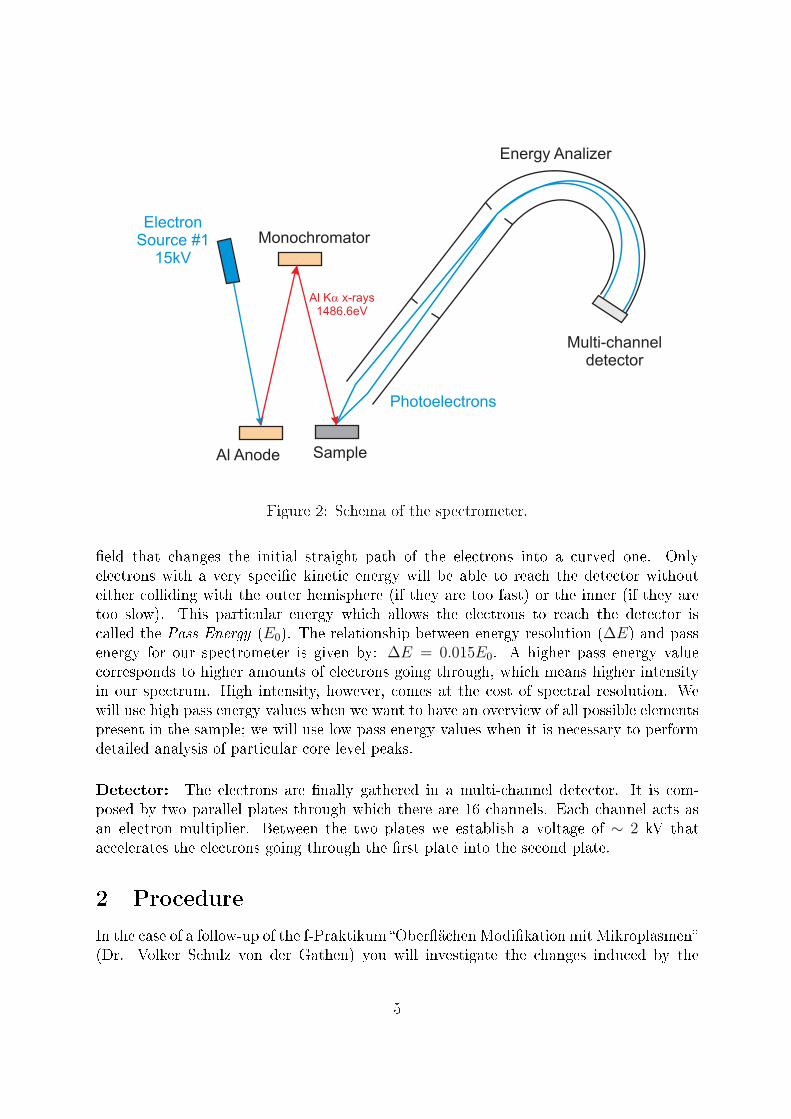
ElectronSource #1
15kV
Al Anode
Photoelectrons
Al K x-rays1486.6eV
a
Sample
Multi-channeldetector
Monochromator
Energy Analizer
Figure 2: Schema of the spectrometer.
�eld that changes the initial straight path of the electrons into a curved one. Onlyelectrons with a very speci�c kinetic energy will be able to reach the detector withouteither colliding with the outer hemisphere (if they are too fast) or the inner (if they aretoo slow). This particular energy which allows the electrons to reach the detector iscalled the Pass Energy (E0). The relationship between energy resolution (∆E) and passenergy for our spectrometer is given by: ∆E = 0.015E0. A higher pass energy valuecorresponds to higher amounts of electrons going through, which means higher intensityin our spectrum. High intensity, however, comes at the cost of spectral resolution. Wewill use high pass energy values when we want to have an overview of all possible elementspresent in the sample; we will use low pass energy values when it is necessary to performdetailed analysis of particular core level peaks.
Detector: The electrons are �nally gathered in a multi-channel detector. It is com-posed by two parallel plates through which there are 16 channels. Each channel acts asan electron multiplier. Between the two plates we establish a voltage of ∼ 2 kV thataccelerates the electrons going through the �rst plate into the second plate.
2 ProcedureIn the case of a follow-up of the f-Praktikum �Ober�ächen Modi�kation mit Mikroplasmen�(Dr. Volker Schulz von der Gathen) you will investigate the changes induced by the
5

plasma treatment on polymers, or on metal surfaces. In this case, we will investigateone un-treated sample and one treated sample in order to establish the chemical changesinduced in the surface due to the plasma treatment.
In the case of a follow-up to the f-Praktikum �402 Anwendungsorientierte Plasma-physik� (Dr. Marc Böke) you will perform a comparative analysis of the bare siliconsurface and of the deposited �lm.
The experimental procedure will be as follows:
1. Sample preparation for the measurement.
2. Low resolution measurement (survey spectrum).
3. High resolution measurements of the relevant core levels.
4. Mathematical analysis of the data and discussion.
2.1 Introduction of the sample in the spectrometerIt is important that the samples are never handled with bare hands, because of tworeasons: to avoid covering the surface of interest with a fat-layer, and to avoid the de-gassing of fat molecules in the UHV environment.
After cutting the sample to an appropriate size, you will mount it on a sample holderand introduce the sample holder in the interchange lock. You need to use the computerin order to vent this interchange lock.
The hardware of the spectrometer is controlled by a single program: PHI SUMMIT.When you click into this icon for the �rst time, three windows will open: Watcher,Acquisition settings, and Image. Watcher will allow you to control the transfer of thesample and the venting and pumping down procedures. Image will allow you to controlthe hardware necessary for the measurement: sample position, neutralizer, ion gun, X-raypower, etc. Acquisition setting will allow you to de�ne your measurement conditions.
How to introduce the sample: First you will introduce your sample in the interchangelock (labelled intro in the window Watcher):
1. Open the N2 bottle. In the window Watcher, press back�ll intro. This will ventthe small chamber on the side of the spectrometer.CAUTION: The top cover of this chamber is not �xed. It can be blown awayif the venting pressure is set too high! As a precaution, always vent with yourhand on top of this cover.
2. After mounting the sample in the fork of the manipulator, cover the chamber againand press pump intro. You will have to wait �ve minutes for the pressure to reacha good value before transferring the sample to the UHV chamber.
6

3. In window Image, go to Stage and press the buttom: intro. This will move the sam-ple stage holder (in the UHV chamber) to the appropriate position for transferringthe sample.
4. In window Watcher, press transfer sample. Follow the instructions in the screen.Once the sample holder is secured in the stage within the UHV chamber, removecarefully the manipulator until the end (when you reach the end position, valve V1will close automatically.)
2.2 Spectrometer start-upSECURITY CONSIDERATIONS.
For your security: Be careful. You are going to operate a machine which producesX-ray radiation by means of accelerating electron beams with high voltage (15kV). Theelectron detector operates also with a voltage of 2kV.
For the security of the machine: The XPS spectrometer operates in ultra highvacuum (UHV). It is important that you always monitor the pressure before starting anyprocedure that will switch on the X-ray tube. If the pressure is higher than 5 · 10−6 Pado not proceed with the measurement.
Once your sample is within the UHV chamber, you need to �nd the right position forthe measurement.
1. In window Image, go to Stage and select a value for the z-position of 16.5 mm. Pressmove. This will move the sample to a good starting position. Now you have to�ne-tune the z-position.
2. By pressing the arrow-buttons in the small box in the screen, move the sample holderand select with help of the camera the position where you want to measure.
3a. If you are measuring conducting samples: In window Image press auto-Z. The soft-ware will �nd the right height for the best measurement. Then go to AcquisitionSettings.
3b. If you are measuring polymers or other non-conducting samples (such as an oxidelayer): you will need to use neutralizing hardware. This implies preparing a sourceof low energy electrons (with the neutralizer) and a source of low energy Ar ions(with the ion gun):
1. First, we prepare the neutralizer. In window Image, go to Neutralizer. If thepressure is in the range of 107 Pa, press Standby.
7

2. Now we prepare the ion gun. (Note that this is also the procedure you haveto follow if you want to use the ion gun in order to sputter the sample). Inwindow Watcher press Di� vlv Open. This will open Valve V4 and closevalve V3.VERY IMPORTANT!Never open the valve that supplies Ar to the ion gun until you are surethat valve V4 is open. The software will not warn you if you make thismistake! If valve V4 is closed when you put Ar to the ion gun, the Arwill enter into the UHV chamber and the pressure will increase withoutcontrol until eventually the security measures of the machine will kick inand all the electronics will be shut o�.
3. In window Image, go to Ion gun. Press Standby. The program will ask youif Valve V4 is open. If you have opened it in the previous step, say Ok (if not,open it now). Now select the extractor pressure box.
4. Open slowly the manual valve (green color) of the ion Gun, controlling simulta-neously the main pressure and the extractor pressure. Open the valve until theextractor pressure shows a value of 30 mPa. At the same time, the pressurein the chamber should not be higher than 4 ·106 Pa. If the pressure in the mainchamber increases over this value without stabilizing, interrupt the procedureimmediately and close the valve.
5. Switch on the valve controller RVG050C (in the rack) with the on/o� blacklever. Now put the white lever limit/set point in the set point position. Waituntil the extractor pressure stabilizes at ∼ 10 mPa. You can now decide ifyou want to use the ion gun in the sputtering mode or in the neutralize mode.Deselect now extractor pressure (the continuous measurement of this pressureis not really necessary and it takes too many resources from the computer).
6. After preparing the neutralizing software, go to window Image, SXI/Auto-Z.Select for Mode [AutoZ] the boxes Neutralizer and Ion Gun Neut.. Go tothe upper right side of the window Image and press auto-Z. The software will�nd the right height for the best measurement. Now you can go to AcquisitionSettings and program your measurement.
2.3 Programming the measurementThe programming of the experiment is performed in the window Acquisition Setting.
First, select the folder where your measurement will be saved, and give a name to yourmeasurement. Following measurements will add a number automatically.
Survey spectrum. Perform always �rst a low resolution measurement with broad en-ergy range. Use the following parameters:
• Range -2, 1200 eV.
8
• Pass energy: 187.85 eV.
• Energy step 0.5 eV.
• Repeats: 1.
• Total Cycles: 5.
In the case of conducting samples: Neutralize OFF. If the case of non-conductingsamples: Neutralize ON.
When everything is ready, press Acquire.
Core level lines. After identi�cation of the di�erent elements present in the sample,you will measure one core level peak of each element (choose the most intense accordingto the Handbook of Photoelectron Spectroscopy [1]). Measurement parameters:
• Range: depends on the region. Select the appropriate range with help of the Ele-ment Table in the window Acquisition Setting.
• Pass energy: 23.5 eV.
• Energy step 0.05 eV.
• Repeats: Will depend on the intensity of the chosen peaks. For the most intensesignals in the spectrum, 10 scans are usually ok.
• Total Cycles: As many as are necessary. Note: you can measure several regionsin the same measurement. In each cycle, the program will measure each region asmany times as you determine with repeats.
If you have conducting samples: NeutralizeOFF. If you have non-conducting samples:Neutralize ON.
When everything is ready, press Acquire.
2.4 Data interpretationIn general, XPS spectra are featured as a plot of intensity vs decreasing binding energy(BE). A typical spectrum consists of well de�ned narrow lines (core level lines) over aelectronic background that increases with increasing BE. The background is formed byelectrons that have su�ered inelastic scattering processes after their emission from theiroriginal atom. The background is continuous because the energy loss processes are randomand multiple.
9
2.4.1 Types of linesSeveral types of lines are observed in a XPS spectra. Some appear always, some de-pend on the particular physical and chemical characteristics of the sample, and some areinstrumental in nature. Here we show a selection of the e�ects relevant to this experiment:
Photoelectron lines These are the narrowest lines observed in the spectra. They aregenerally symmetric, although pure metals can exhibit considerable asymmetry dueto interaction of photoelectrons with conduction electrons.
Auger lines The re�lling of the inner shell vacancy left by the emission of an electroncan be done by radiative (�uorescence) or non radiative(Auger) processes. However,in the energy range where we will work (∼ 1 keV), Auger will be the predominant�lling mechanism. Radiative processes compete with Auger only for transition en-ergies of ≥ 10 keV. Therefore, in addition to photoelectrons emitted through thephotoe�ect, Auger electrons will be emitted because of the relaxation of the excitedions remaining after photoemission. In an Auger process (which occurs roughly10−14 seconds after the photoelectric event), an outer electron falls into the innerorbital vacancy, and a second electron is simultaneously emitted, carrying o� theexcess energy. The kinetic energy of the Auger electron is equal to the di�erence be-tween the energy of the initial ion and the doubly charged ion, and it is independentof the mode of the initial ionization. There are four main Auger series observablein XPS. They are the KLL, LMM, MNN and NOO series.
Spin-orbit splitting Due to spin-orbit interactions (j=l±s), the p,d, and f levels splitduring ionization, leading to vacancies in the p1/2 and p3/2 (l=1), d3/2 and d5/2 (l=2)orbitals and so on.The relative intensities of the doublet components depend on the multiplicity of thestates, given by the available amount of di�erent magnetic states (di�erent possiblevalues of the quantum number mz: 2j + 1 di�erent possible numbers). Therefore,the spin-orbit splitting ratio is 1:2 for p levels, 2:3 for d levels and 3:4 for f levels.
Energy loss lines With some materials, there is the possibility of losing certain amountof energy due to interaction between the photoelectron and other electrons in thesurface region of the sample. In insulators these lines are not very intense, and canbe rather broad. However, in metals the e�ect is much more dramatic. Energyloss to the conduction electrons occurs in well de�ned quanta characteristic of eachmetal. These plasmons arise from group oscillations of the conduction electrons.The photoelectron line is mirrored at intervals of higher BE with reduced intensity.The energy interval between the main peak and the loss peak is called the plasmonenergy. The so-called bulk plasmons are the more prominent of these lines. A secondseries, the surface plasmons, exists at energy intervals determined approximately bydividing the energy of the bulk plasmon by
√2. For insulators, usually only the �rst
plasmon peak is seen.
10
Valence bands These signals are produced by photoelectron emission from molecularorbitals and from solid state energy bands. Di�erences between insulators andconductors are specially noted by the absence of presence of electron from conductionbands at the Fermi level.
2.4.2 Chemical ShiftThe core electron of an element has a unique binding energy, like a ��ngerprint�. Thusalmost all elements except for hydrogen and helium can be identi�ed by measuring thebinding energy of its core electron. Furthermore, the binding energy of core electrons issensitive to the chemical environment of element. The in�uence of the chemical environ-ment can be seen as a shift of the binding energy of the corresponding XPS peak, rangingfrom 0.1 eV to 10 eV. This e�ect is called �chemical shift�.
The chemical shift is therefore the di�erence between the energy of a photoelectronline for an element in a speci�c compound and the corresponding energy for the elementin its pure state. The chemical shift is frequently reported in publications and handbooks.As an example you can see in Figure 3 the C1s core level of a PET (Polyethylene tereph-thalate) sample. The carbon atoms of the polymer �see� a di�erent chemical environmentdepending on their position within the polymer chain. Di�erent chemical environmentsresult in di�erent chemical shifts, which we can analyze also quantitatively. This fact isthe essence of the utility of XPS for chemical analysis, and the reason why it is also knownas electron spectroscopy for chemical analysis (ESCA).
Note: you might �nd apparent shifts in binding energy positions that are not due to achemical shift! This refers to the two e�ects discussed previously: �oating Fermi energylevel of the sample, and sample charging (see Section 1).
2.5 Mathematical treatment of the data: Fitting procedure andchemical state identi�cation
The identi�cation of chemical states depends primarily on the accurate determinationof line energies. Once we have e�ectively determined the line positions, we can startdigging into the chemical composition determination problem by looking at the providedliterature.
In order to get a precise value for the binding energy position of each peak, we will�t the experimental data with a mathematical model. The peak shape for XPS spectrais best described by a convolution of the natural line width, the width of the x-ray linewhich created the photoelectron line, and the instrumental contribution. Additionally, insome cases we have to consider an asymmetry factor (in the case of metallic components.).
With the Multipak program, we will however simulate the line pro�le with a product ofa Gaussian and a Lorentzian lines. The Gaussian component accounts for the instrumentalbroadening, chemical disorder, charging, etc; the Lorentzian function accounts for the�nite lifetime of the core-hole in the photoionization process. The mathematical analysis
11
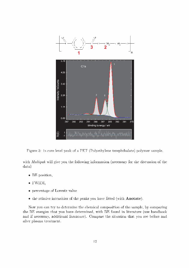
Figure 3: 1s core level peak of a PET (Polyethylene terephthalate) polymer sample.
with Multipak will give you the following information (necessary for the discussion of thedata)
• BE position,
• FWHM,
• percentage of Lorentz value
• the relative intensities of the peaks you have �tted (with Anotate).
Now you can try to determine the chemical composition of the sample, by comparingthe BE energies that you have determined, with BE found in literature (use handbookand if necessary, additional literature). Compare the situation that you see before andafter plasma treatment.
12

Quantitative analysis Since the number of photoelectron of an element is dependentupon the atomic concentration of that element in the sample, XPS is used to not onlyidentify the elements but also quantify the chemical composition.
In many cases it is important to be able to quantify the relative concentrations ofthe various constituents of the sample surface. In order to do this we will use the peakareas together with tabulated sensitivity factors. The program Multipak will perform thisquantitative analysis automatically, when you press the % symbol on the top right areaof the window. For detailed information on the procedure behind this simple mouse click,you can read the rest of this section.
For a sample homogeneous in the analysis volume, the number I of photoelectrons persecond in a speci�c spectra peak is given by:
I = nfσθyλAT
n: Number of atoms of the element per cm3 of the sample.
f: X-ray �ux in photons/cm2s
σ: Photoelectric cross section for the atomic orbital of interest in cm2.
θ: Angular e�ciency factor for the instrumental arrangement based on the angle betweenthe photon path and the detected electron.
y: E�ciency in the photoelectric process for formation of photoelectrons.
λ: Mean free path of the photoelectrons in the sample
A: Area of the sample from which photoelectrons are detected
T: Detection e�ciency for the electrons emitted from the sample
We are interested in n, which we can write as:
n =I
fσθyλAT≡ I
S
.The factors contained in S are either a characteristic of the spectrometer, or have a
weak dependence from sample to sample, so that, if we have an homogeneous sample, wecan establish the following relationships between peaks from di�erent elements:
n1
n2
=I1S1
I2S2
where, for each spectrometer, it is possible to determine the values of S for all elements.Note that these concrete values will be applicable only to a particular spectrometer, sincethey also need to be corrected by a transmission function typical of each machine.
13
So now, a general expression for determining the atom fraction of any constituent ina sample Cx can be written simply as:
Cx =nx∑ni
=Ix/Sx∑Ix/Sx
2.6 ReportFor the report, discuss the following points about your measurements:
• Identify all the features observed in the survey spectra.
• Using the core level spectra, discuss quantitatively the chemical composition of thesample before and after the plasma treatment.
Apart from the discussion relevant to the samples that you have investigated, you canuse the following set of questions to help you shape your report:
• What is the photoe�ect?
• What is the Auger-E�ect?
• What kind of information can we get from XPS?
• What features do we expect to see in a XPS spectrum? What is the origin of thesestructures? What is the approximate range of detectable BEs of all detectable linesby Al radiation?
• Why does the background level increase abruptly after each line?
• What is the so-called �chemical shift� in XPS?
• What is the origin of charging problems in XPS measurements? What can we doagainst it? What are the di�culties involved in the determination of a bindingenergy reference in the case of non conducting samples?
References[1] J F Moulder, W F Stickle, P E Sobol, K D Bomben. Handbook of X-ray
Photoelectron Spectroscopy. Published by ULVAC-PHI, 1995.
14


![Welcome [] · This X-ray Photoelectron Spectrometer (XPS) system with high resolution scanning field emission Auger system (AES), Ultraviolet Photoelectron Spectroscopy (UPS) and](https://img.pdfslide.us/doc/110x75/6112edfd9b5bbe153f6ae88c/welcome-this-x-ray-photoelectron-spectrometer-xps-system-with-high-resolution.jpg)