Embed Size (px)
Citation preview

Network for Computational Nanotechnology (NCN)Purdue, Norfolk State, Northwestern, MIT, Molecular Foundry, UC Berkeley, Univ. of Illinois, UTEP
Electronic and Thermal properties of semiconductor nanostructures:A modeling and simulation study
Abhijeet PaulNetwork for Computational Nanotechnology
(NCN),Electrical and Computer Engineering
Purdue Universityemail: [email protected]

Abhijeet Paul
Acknowledgements• Overall guidance and direction
» Prof. Gerhard Klimeck, Prof. Mark Lundstrom, Purdue University, USA.
» Prof. Timothy Boykin, University of Alabama at Huntsville, USA (PhD committee member).
» Prof. Leonid Rokhinson, Purdue University, USA (PhD committee member).• Theory and Code development
» Dr. Mathieu Luisier, ETH Zurich, Switzerland (OMEN/OMEN-BSLAB development).
» Prof. Timothy Boykin, University of Alabama Huntsville, USA (Tight-Binding and solid state phys. theory)
» Dr. Neophytos Neophytou, TU Wien, Austria (Initial MATLAB codes)• Discussions and work
» Saumitra Mehrotra, Parijat Sengupta, Shuaib Salamat, Sunhee Lee, Lang Zeng, Mehdi Salmani, Kai Miao, Dr. Raseong Kim and Changwook Jeong, Purdue University.
• .Experimental Collaborators
» Dr. Giuseppe Tettamanzi, TU Delft, Netherlands, Shweta Deora, IIT Bombay, India, Dr. Subash Rustagi, IME, Singapore, Dr. Mark Rodwell, UCSB, USA.
• Summer Undergrad students (for nanohub tools)
» Junzhe Geng, Victoria Savikhin, Mohammad Zulkifli, and Siqi Wang, Purdue University.• Funding and Computational Resources
» MSD-FCRP, SRC, NSF and MIND for funding.
» NCN and nanoHUB.org for computational resources.
2

Abhijeet Paul
PhD timeline and progress
[A] N. Singh et. al, EDL 2006 [B] A. Hochbaum et. al, Nature, 2008 [C] Yu et. al, Nature, 2010. [D] Pernot et. al, Nature, 2010.
Important experimental works that guided this PhD work.Important experimental works that guided this PhD work.
3
Abhijeet Paul
Outline of the talk
• Motivation» Why the present work is important ?
» Need for integrated atomistic simulation framework
• Computational modeling and simulation approaches.
• Application of the methods to Si nanowires (SiNWs).
• Application to non-Si system GaAs a quick look !!
• Global dissemination of findings nanoHUB.org
• Summary
• Future directions
4

Abhijeet Paul
Mo
re Mo
ore(M
M)
Beyo nd
Si
More than Moore(MtM) Beyond CMOS
90nm90nm
65nm65nm
45nm45nm
32nm32nm
22nm22nm
Baselin
e CM
OS
: CP
U, M
emo
ry, Lo
gic
Analog RF
Analog RF SensorSensorThermo
electricityThermo
electricity Bio-chipsBio-chips
Added Functional Diversity: More interaction
Sensory parts:
Measuring and
sense surrounding
Brain:Computation and
Calculations
Hig
her
Valu
e S
yste
ms
Faster processing and better interaction with environment holds the key to next-gen technologies.
MM and MtM are the solutions !!!
Faster processing and better interaction with environment holds the key to next-gen technologies.
MM and MtM are the solutions !!!
How to get more ???
5

Abhijeet Paul
ITRS
CMOS scaling challenges
Intel
Need higher
processing
Speed !!!
Need for f
aster
Transistors!!!
CMOS challengesCMOS challenges
New MaterialsNew Materials SiNW FET
New device structure
New device structure
Next-gen CMOS scaling solutions More MooreNext-gen CMOS scaling solutions More Moore6
Revolutionary Evolutionary

Abhijeet Paul
www.tellurex.com
Choudhary et. al, Nature nano. (2009)
Why thermoelectricity ???
Increasing
pollutio
n!!!
IEA, WEO, 2008
Increasing energy
demand!!!
Gelsinger et. al ISSCC 2001
Increasing IC
heat!!!
Nasty Problems Nasty Problems
On chip thermoelectric
cooling (BiTe SL)
DEER
Automobile wasteheat thermoelectricpower generation Green energy
Production bythermoelectricity
Green Solutions from thermoelectricity More than MooreGreen Solutions from thermoelectricity More than Moore7

Abhijeet Paul
Dimensional Scaling: CMOS 20
03
2005
2007
2009
2011
Strain Tec hno
lo gy
High- k
Meta
l Gate 3DF
ET
S
SiGe strained
High-KMG
From bulk planar to 3D nano-scale
SiNW FET
III-V FET
Graphene
CNT-FET
Non-Si3D FETs
are a solution
Non-Si3D FETs
are a solution
???
8
IBM
Abhijeet Paul
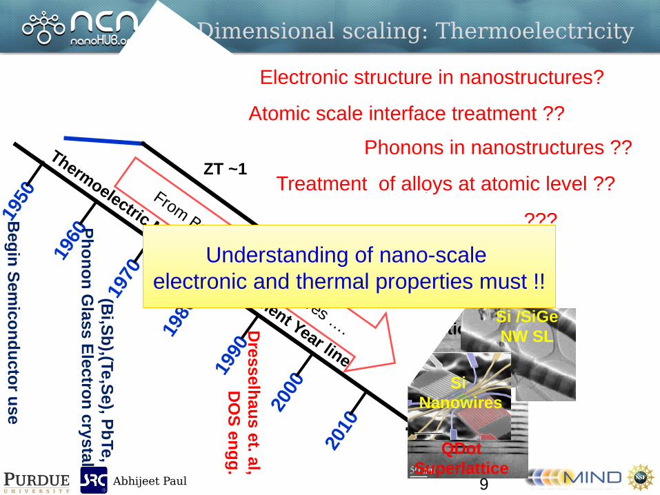
Dimensional scaling: Thermoelectricity
BiTe/PbTeQwell
Superlattice
SiGe/SiQDot
Superlattice
BiTe,PbTe Bulk
LAST
1950
2000
1990
1980
1970
1960
2010
Thermoelectric Material development Year line
Beg
in S
emico
nd
ucto
r use
(Bi,S
b) ,(Te,S
e ), Pb
Te , P
ho
no
n G
lass Electr o
n cry stal
Dresse lh
aus e t. al,
DO
S en
gg
.
PbTe Ddots
Si /SiGeNW SL
Si Nanowires
ZT ~1
1< ZT < 3ZT > 3
From Bulk to Nanostructures ….
9
Atomic scale interface treatment ??
Phonons in nanostructures ??
Treatment of alloys at atomic level ??
Electronic structure in nanostructures?
??????
Understanding of nano-scale electronic and thermal properties must !!
Understanding of nano-scale electronic and thermal properties must !!

Abhijeet Paul
Need for Atomic level modeling…
Si n-FinFETIMEC
H=65nm,W=25nmG. Tettamanzi et. al, EDL, 2009.
IntelSiGe pMOSFETIEDM 2010
Ultra-scale geometry with
finite atoms
Ultra-scale geometry with
finite atoms
An increasing need for atomic scale
modeling to simulate ultra-
scaled devices!!!
An increasing need for atomic scale
modeling to simulate ultra-
scaled devices!!!10
http://www.xray.cz/xray/csca/kol2010/abst/cechal.htm
Quantum DotMaterial variation at atomic scale
Material variation at atomic scale
Atomic scale strain variationAtomic scale
strain variation

Abhijeet Paul
Need for integrated device modeling …
SiGe
SiSiO2
Treatment of multiple valleysTreatment of
multiple valleys
Treatment of multiple materials
Treatment of multiple materials
Electron current Phonons
Treatment of multiple particles
Treatment of multiple particles
An increasing need for integrated
modeling to handle complex issues in device
modeling !!!
An increasing need for integrated
modeling to handle complex issues in device
modeling !!!
11

Abhijeet Paul
ITRS on the future device modeling ...
ITRS 2010, chapter 9, http://www.itrs.net
Physical models for stress induced device performance.
Physical models for novel materials eg. High-k stacks, Ge and compound III/V channels: … Morphology, Bandstructure, defects/traps,etc.
General , accurate, computationally efficient and robust quantumbased simulators incl. fundamental parameters linked to electronicbandstructure and phonon spectra.
Treatment of individual dopant atoms and traps…
Need for an integrated approach to model material, electronic and lattice properties at the atomic scale.
Need for an integrated approach to model material, electronic and lattice properties at the atomic scale.
12

Abhijeet Paul
Outline of the talk
• Motivation
»Why the present work is important ?
»Need for integrated atomistic simulation framework
• Computational modeling and simulation approaches.
• Application of the methods to Si nanowires (SiNWs).
• Application to non-Si system GaAs a quick look !!
• Global dissemination of findings nanoHUB.org
• Summary
• Future directions
13

Abhijeet Paul
How to study the nano-scale devices?
Bottom-up Approach
To nano-scale
devices
Bottom-up Approach
To nano-scale
devicesEle
ctro
nic
Stru
ctur
e Lattice Structure
Carrier Transport
AtomisticTight-binding
(TB)model
AtomisticTight-binding
(TB)model
14

Abhijeet Paul
<111>
Atomistic Tight binding Approach
15
Crystal structureCrystal structure
FEATURES/ADVANTAGESNearest neighbor atomic bond model with spin orbit (SO) coupling. Based on localized atomic orbital treatment. Appropriate for treating atomic level disorder. Strain treatment at atomic level. Structural and material variation treated easily. Potential variations can be accounted for (easily).
FEATURES/ADVANTAGESNearest neighbor atomic bond model with spin orbit (SO) coupling. Based on localized atomic orbital treatment. Appropriate for treating atomic level disorder. Strain treatment at atomic level. Structural and material variation treated easily. Potential variations can be accounted for (easily).
Y
Z
<100>
(x)<110>StructureStructure
OrbitalOrbitalInteractionInteraction
Assemble Assemble TB HamiltonianTB Hamiltonian
Atomistic Tight Binding (TB)A reliable way to calculate electronic structure in ultra-scaled structures.
Atomistic Tight Binding (TB)A reliable way to calculate electronic structure in ultra-scaled structures.
15

Abhijeet Paul
Bulk Bandstructure using Tight-binding
Si
Lent et. al, Superlat. and Microstruc., 1986
Pb
Se
sp3d5s*-SO model
sp3d5-SO model
Γ VB L
X CB L
Atomistic Tight-Binding method A robust and accurate electronic structure model
Atomistic Tight-Binding method A robust and accurate electronic structure model
ZincblendeRocksalt
LL
16

Abhijeet Paul
Application of TB to FETs: Charge-potential self-consistent approach
Schrodinger-Poisson self-consistent solution Electron transport analysis in nano-scale FETs.Schrodinger-Poisson self-consistent solution Electron transport analysis in nano-scale FETs.
17

Abhijeet Paul
Experimental validation of 2D atomistic Schrodinger-Poisson simulator
Collaboration between Purdue University & Institute of Microelectronics, Singapore (2007-08).
TEM image of Experimental SiNW FET
Device Dimensions:Tox = 9nmW = 25nmH = 14 nmSource/Drain doping : n-type ,1e20cm-3
Intrinsic <100> oriented Silicon channel.
Schrodinger using TB
2D FEM Poisson solution
4505 atoms4505 atoms
~20K FEM elements~20K FEM elements
chargechargepotentialpotential
Self-consistent Simulation
Self-consistent simulation of realistic devices using parallel C/C++ code.
Self-consistent simulation of realistic devices using parallel C/C++ code.
18

Abhijeet Paul
Experimental validation of atomistic simulator contd.
Electrical Potential Distribution.
Electron charge distribution
Self-consistent SimulationTerminal CV benchmarking
Good matchingGood matching
Impact: Work published in IEEE, EDL VOL. 30, NO. 5,MAY 2009. p.526 Impact: Work published in IEEE, EDL VOL. 30, NO. 5,MAY 2009. p.526
Simulator benchmarked !!!Quantum mechanical simulations for realistic FETs possible.
Simulator benchmarked !!!Quantum mechanical simulations for realistic FETs possible.
19

Abhijeet Paul
How to study the nano-scale devices?
Bottom-up Approach
To nano-scale
devices
Bottom-up Approach
To nano-scale
devicesEle
ctro
nic
Stru
ctur
e Lattice Structure
Carrier Transport
AtomisticTight-binding
(TB)model
AtomisticTight-binding
(TB)model
Modified Valence Force Field (MVFF)
model
Modified Valence Force Field (MVFF)
model
20

Abhijeet Paul
Phonon dispersion calculation:Modified VFF (MVFF) model
Old KeatingModel [1]
[A]
Bond-stretching(α)
Δr
[B]
Bond-bending(β)
Δθ
[C] Cross-bondstretch bend (γ)
[2] Zunger et. al. 1999ΔθΔr
Imp. For polar materials [2]
Imp. for polar
materials [2]
[F]
Coulomb interaction
[E]
Δθ1
Δθ2
Coplanar bond bending(τ)
Imp. for non-polar materials ([3] Sui et. al,
1993)
[D]
Δr1Δr2
Cross bondStretching (δ)
Short RangeShort Range
[1] Keating. Phys. Rev. 145, 1966.[2] PRB, 59,2881, 1999.[3] PRB, 48, 17938,1993
Long RangeLong Range
21
New combination of Interactions:Modified Valence Force Field
Calculate phonons in zinc-blende materials.
New combination of Interactions:Modified Valence Force Field
Calculate phonons in zinc-blende materials.

Abhijeet Paul
Bulk Si
Expt. (dots) [1]
What is the need for a new phonon model??
Accurate phonon model crucial for correct calculation of phonon dispersion in nanostructures.
Accurate phonon model crucial for correct calculation of phonon dispersion in nanostructures.
Bulk Si
Expt. (dots) [1]
[1] Nelsin et. al, PRB, 6, 3777, 1972. 22
Keating VFF Model
Over estimates acoustic modes at zone edges.
Over estimates optical modes
New MVFF model matchs the dispersion very well in the entire
Brillouin zone !!!
Expt. Data[1], inelastic neutron scattering (80K and 300K).
Expt. Data[1], inelastic neutron scattering (80K and 300K).
Abhijeet Paul
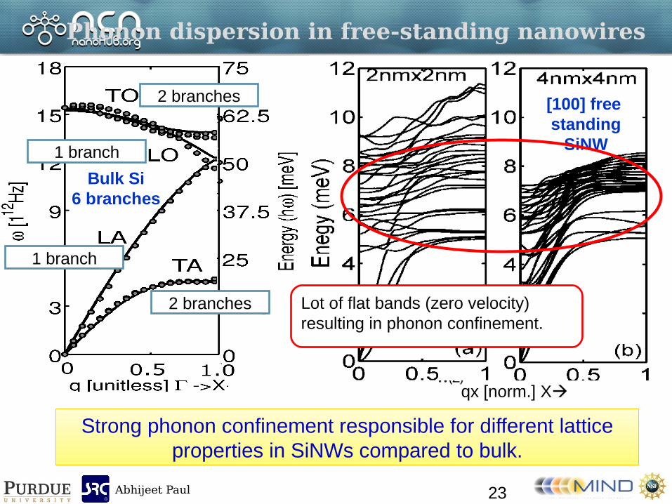
1D periodic [100] Si nanowire structure.
Surface atoms free to vibrate.
1D periodic [100] Si nanowire structure.
Surface atoms free to vibrate.
[100] free standing
SiNW
qx [norm.] X
Bulk Si6 branches
Phonon dispersion in free-standing nanowires
23
Strong phonon confinement responsible for different lattice properties in SiNWs compared to bulk.
Strong phonon confinement responsible for different lattice properties in SiNWs compared to bulk.
Lot of flat bands (zero velocity) resulting in phonon confinement.
2 branches
1 branch
1 branch
2 branches

Abhijeet Paul
Approaches to study the nano-scale devices
Bottom-up Approach
To nano-scale
devices
Bottom-up Approach
To nano-scale
devicesEle
ctro
nic
Stru
ctur
e Lattice Structure
Carrier Transport
AtomisticTight-binding
(TB)model
AtomisticTight-binding
(TB)model
Modified Valence Force Field (MVFF)
model
Modified Valence Force Field (MVFF)
model
Landauer’s model (LM)Landauer’s model (LM)
24

Abhijeet Paul
Material A
Material B
How to analyze thermoelectric properties of materials ?
V1
V2
INOUT
Tc Th
IQ
Ie
Ie
Steady-state linear thermoelectric (Onsager’s) relations [1,2]
[1] L. Onsager, Phys. Rev. 37 405 (1931).[2] G. D. Mahan, Many-body Physics.
lehhch TTTTTTVVV ,2,,21
TT q
TkV BLandauer’s Formula can be used to
evaluate the transport parameters Landauer’s Formula can be used to evaluate the transport parameters
TTGSVTGSIQ .. 2 TGSVGIe ..Electric current Heat current
25

Abhijeet Paul
Goodness of thermoelectric materials:Figure of Merit (ZT)
T
V
S
Generation of potential difference due to applied temperature difference`Seebeck Coefficient’.
Generation of potential difference due to applied temperature difference`Seebeck Coefficient’.
Generation of temperature difference due to applied potential difference `Peltier Coefficient’
Generation of temperature difference due to applied potential difference `Peltier Coefficient’
Measure of thermoelectric power generation (High)
T
VT
Measure of thermoelectric
cooling (High)
Ability of material to conduct electricity `Electrical Conductance’Ability of material to conduct electricity `Electrical Conductance’
V
IG
Measure of charge flow (High)
d
Q
T 1
Ability of material to conduct heat energy `Thermal Conductance’Ability of material to conduct heat energy `Thermal Conductance’
Measure of heat flow (Low)Both electrons (ke)and lattice(kl) carry heat.
ZT = ‘Thermoelectric Figure of Merit’ by Ioffe in 1949. S2G = Electronic Power Factor (PF)
ZT = ‘Thermoelectric Figure of Merit’ by Ioffe in 1949. S2G = Electronic Power Factor (PF)el
TGSZT
2
26
High ZT large G large S and small κ desired !!! High ZT large G large S and small κ desired !!!

Abhijeet Paul
Calculation of thermoelectric parameters
27
)(factor-Pre / lemLf
G,Sκe
(Electronic)
Landauer’s approach A suitable approach to calculate
thermoelectric transport parameters in nanostructures.
Landauer’s approach A suitable approach to calculate
thermoelectric transport parameters in nanostructures.
κl (Lattice)Landauer’s IntegralLandauer’s Integral
Under zero current condition
eLG 0 ee LLS 01 / ll L1

Abhijeet Paul
A closer look at electrons and phonons
28
max
0
)()()(
dM
T
F
LL BEphml
m Phonon IntegralPhonon Integral
Etop
FDel
m
B
em dEEM
E
EF
L
E
Tk
EfEL )(
)()(Electron IntegralElectron Integral
lemL / •No. of modes, M(E).
•Mean free path (λ).
Both need
•Moment calculation near Fermi Level•Fermi Dirac distribution (fermions!!)•M(E) Electronic bandstructure.
Electrons need
•No Fermi Level•Bose Einstein distribution (bosons!!)• M(ω) Phonon dispersion.
Phonons need
Accurate electronic & phonon dispersions must !!!.
Accurate electronic & phonon dispersions must !!!.

Abhijeet Paul
The complete approach set
Bottom-up Approach
To nano-scale
devices
Bottom-up Approach
To nano-scale
devicesEle
ctro
nic
Stru
ctur
e Lattice Structure
Carrier Transport
AtomisticTight-binding
(TB)model
AtomisticTight-binding
(TB)model
Modified Valence Force Field (MVFF)
model
Modified Valence Force Field (MVFF)
model
Landauer’s model (LM)Landauer’s model (LM)
Electronic PropertiesElectronic Properties
Thermal PropertiesThermal
Properties
ThermoelectricityThermoelectricity
An ‘integrated approach’ to study electronic, physical and thermal properties of nanostructures !!!
An ‘integrated approach’ to study electronic, physical and thermal properties of nanostructures !!!
29

Abhijeet Paul
Outline of the talk
• Motivation
»Why the present work is important ?
»Need for integrated atomistic simulation framework
• Computational modeling and simulation approaches.
• Application of the methods to Si nanowires (SiNWs).
• Application to non-Si system GaAs a quick look !!
• Global dissemination of findings nanoHUB.org
• Summary
• Future direction
30

Abhijeet Paul
SiNW
Explosive -sensor [E]
Silicon nanowires (SiNW): The vast potential
[A] Yang et. al, 2010, Nanoletters.[B] Kalzenberg et. al, 2008, Nanoletters. [C] Chin et. al, 2009, IEEE, TED. [D] Hochbaum et. al, 2008, Nature.[E] Patlosky et. al, 2010, Verlag, Germany.
CathodeLi2S
AnodeSiNW
Batteries [A]
Siliconnanowire
Solar cells [B]
Transistors [C]
Thermoelectricity [D]SiNWs have versatile applicationsand
are highly compatible to CMOS. Interesting system to study!!!
SiNWs have versatile applicationsand
are highly compatible to CMOS. Interesting system to study!!!
31

Abhijeet Paul
Nanoscale solutions in SiNWs
Siliconnanowire
Physical metrologyHow to determine size, shape and
orientation ?
Electrical metrologyHow to determine
interface traps in SiNW FETs?
Thermal propertiesHow to engineer
thermal properties of SiNW ?
ThermoelectricityHow to enhance PF and ZT of SiNW ?
??
32

Abhijeet Paul
Peeking into the channel of Si trigated n-FinFETs
33
Collaboration between Purdue University ,TU Delft, Netherlands and IMEC, Belgium (2009-2011).
TEM image of tri-gated n-FinFETs
Active Area(SAA)
Where do the charges flow ?
source
Channel
Barrier Height (Eb)
How easily charges go from
source to channel?
TemperatureBased G-V
measurement
Experiment
From slope
From intercept
Sub-threshold thermionic current provides information about undoped channel Si FinFETs !!!
Sub-threshold thermionic current provides information about undoped channel Si FinFETs !!!
Abhijeet Paul
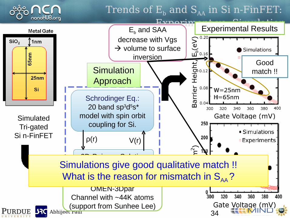
Trends of Eb and SAA in Si n-FinFET: Experiment vs. Simulation
34
Experimental ResultsEb and SAA decrease with Vgs
volume to surface inversion
SimulatedTri-gated
Si n-FinFET
Schrodinger Eq.: 20 band sp3d5s*
model with spin orbit coupling for Si.
Schrodinger Eq.: 20 band sp3d5s*
model with spin orbit coupling for Si.
2D-Poisson Solution2D-Poisson Solution
ρ(r) V(r)
SimulationApproach SimulationApproach
Performed using OMEN-3Dpar
Channel with ~44K atoms(support from Sunhee Lee)
Goodmatch !!
???Simulations give good qualitative match !!What is the reason for mismatch in SAA ?
Simulations give good qualitative match !!What is the reason for mismatch in SAA ?

Abhijeet Paul
Mismatch in SAA :Interface trap density (Dit) extraction
35
A
B
3D FinFETs bad sidewall etch [1] interface traps gate screened from channel mismatch in SAA
[1] Kapila et. al, IEEE, EDL, 2008
FromCharge
Neutrality
~2X~2X
No H2 anneal More mismatch!!
No H2 anneal More mismatch!!
A. Paul et. al, JAP, 2011
Difference in expt. and simulated SAA Dit extraction Method 1
H2 anneal reduce traps by ~2X.
Difference in expt. and simulated SAA Dit extraction Method 1
H2 anneal reduce traps by ~2X.

Abhijeet Paul
Mismatch in Eb :Interface trap density (Dit) extraction
36Gate Voltage (V)
Eb
(meV
) H2 anneal
H2 anneal
3D FinFETs bad sidewall etch [1] interface traps gate screened from channel mismatch in Eb
g
bV
E
Gate to Channel coupling.Suppressed by interface
traps
Dit ~18.1x10¹¹#/cm2
Dit ~15.3x10¹¹#/cm2
[110]
Dit ~10.3x10¹¹#/cm2
[100]Difference in expt. and simulated α Dit extraction Method 2
[110] sidewall Dit > [100] sidewall Dit.
Difference in expt. and simulated α Dit extraction Method 2
[110] sidewall Dit > [100] sidewall Dit.
A.Paul et. al, JAP, 2011

Abhijeet Paul
ConductanceMeasurement
and simulations.
ConductanceMeasurement
and simulations.
Siliconnanowire
Physical metrologyHow to determine size, shape and
orientation ?
Electrical metrologyHow to determine
interface traps in SiNW FETs?
Thermal propertiesHow to engineer
thermal properties of SiNW ?
ThermoelectricityHow to enhance PF and ZT of SiNW ?
??
37

Abhijeet Paul
Physical Metrology Raman Spectroscopy: A primer
Fre
qu
ency
(cm
-1)
Intensity (a.u)
Bulk Material
Nanostructure(NS)
Phonon Shift Raman
Spectrometer
Phonon Shift Raman
Spectrometer
Acoustic Phonon
shift
Acoustic Phonon
shift
q Fre
qu
ency
(ω)
Optical Phonon
shift
Optical Phonon
shift
q Fre
qu
ency
(ω)
Bulk/
NS// acoptacoptacopt
2 types of shifts
∆ω > 0 Blue-shift∆ω < 0 Red-shift
Info on size, dimensionality,
crystallanity of nanostructuresPhonon shifts provide vital information about
Physical properties of nanostructures!!!Phonon shifts provide vital information about
Physical properties of nanostructures!!!
38

Abhijeet Paul
Phonon shifts: Experimental benchmarking.
Acoustic hardening or blue-shiftin SiNWs
Acoustic hardening or blue-shiftin SiNWs
Optical softening or red-shift in SiNWs
Optical softening or red-shift in SiNWs
39
d
W
aA 0
Connects to dimensionality
of NS Connects to the
shape of the nanowire in 1D
MVFF compares
with expts. very well
Acousticd <1
for 1D. A >0
Opticald >1
for 1D.A < 0
MVFF provides correct trend for phonon shifts ‘A’ and ‘d’ correlation can connect to
SiNW shape
MVFF provides correct trend for phonon shifts ‘A’ and ‘d’ correlation can connect to
SiNW shape

Abhijeet Paul
Physical metrology of SiNWs
40
SiNW shapes under study
d
W
aA 0
‘A’ and ‘d’ from acoustic and optical phonon shifts correlate to
SiNW shape nanoscale metrology
‘A’ and ‘d’ from acoustic and optical phonon shifts correlate to
SiNW shape nanoscale metrology

Abhijeet Paul
ConductanceMeasurement
and simulations.
ConductanceMeasurement
and simulations.
Siliconnanowire
Physical metrologyHow to determine size, shape and
orientation ?
Electrical metrologyHow to determine
interface traps in SiNW FETs?
Thermal propertiesHow to engineer
thermal properties of SiNW ?
ThermoelectricityHow to enhance PF and ZT of SiNW ?
Raman spectroscopyPhonon shift
in SiNWs
Raman spectroscopyPhonon shift
in SiNWs
??
41

Abhijeet Paul
Heat SinkHeat Sink
BB
AA
Heat SourceHeat Source
Thermoelectric device
Need for tuning material thermal properties
42
Hea
t F
low
Thermal Capacitance
VCV thC
Equivalent thermal circuit
Thermal Resistance
L
A
th
thR
Engineering material thermal properties can improve system performance!!!
Engineering material thermal properties can improve system performance!!!
Better Laser CoolingBetter Heat evacuation
in FETs.Improved ZT in
thermoelectric devices

Abhijeet Paul
Strain: Tuning thermal conductivity of SiNWs
Set-up
Expt.Result
Gan et.alPurdue University
MVFF simulations show similar tuning for thermal conductivity
with strain.
MVFF simulations show similar tuning for thermal conductivity
with strain.
SimulationMVFF
A. Paul et. al, APL, 2011.
43
Abhijeet Paul
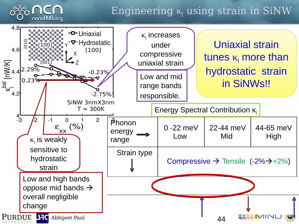
Engineering κl using strain in SiNW
Phonon energy range
0 -22 meVLow
22-44 meVMid
44-65 meVHigh
Strain type Compressive Tensile (-2%+2%)
Uniaxial 36%34% 52%50% 12%13%
Hydrostatic 32%37% 56%45% 11%16%
44
Energy Spectral Contribution κl
κl increases under
compressiveuniaxial strain
κl is weakly sensitive to hydrostatic
strain
Low and mid range bands
responsible.
Low and high bands oppose mid bands overall negligible change
Uniaxial strain tunes κl more than hydrostatic strain
in SiNWs!!
Uniaxial strain tunes κl more than hydrostatic strain
in SiNWs!!

Abhijeet Paul
Tuning Specific heat (Cv) of SiNWs using strain
45
Uniaxial strain brings neglible change to Cv
Very less change In energy
contribution under strain
Hydrostatic strain brings large change
to Cv
Higher energy bands contribute to the change in Cv.
Hydrostatic strain tunes Cv more than uniaxial strain in SiNWs !!!
Hydrostatic strain tunes Cv more than uniaxial strain in SiNWs !!!

Abhijeet Paul
ConductanceMeasurement
and simulations.
ConductanceMeasurement
and simulations.
Siliconnanowire
Physical metrologyHow to determine size, shape and
orientation ?
Electrical metrologyHow to determine
interface traps in SiNW FETs?
Thermal propertiesHow to engineer
thermal properties of SiNW ?
ThermoelectricityHow to enhance PF and ZT of SiNW ?
Strain tunes Phonon thermal
properties
Strain tunes Phonon thermal
properties
??
Raman spectroscopyPhonon shift
in SiNWs
Raman spectroscopyPhonon shift
in SiNWs
46

Abhijeet Paul
Porous crystalline Si for thermoelectricity
Hopkins et.al Nano. Lett.,
2011.
Tang et.al Nano Lett., 2010.
Yu et. al Nature Nanotech.
2010
Electrical Conductivity[1]
Electrical Conductivity[1]
~1.5X Drop
Thermal Conductivity[1]
Thermal Conductivity[1]
~8X Reduction
Experimental structures
Experimental structures
Experimental results
Experimental results
[1] Yu et. al Nature Nanotech., 2010.
Porous Silicon an attractive alternative for RT thermoelectric material. How about porous SiNWs ?
Porous Silicon an attractive alternative for RT thermoelectric material. How about porous SiNWs ?
47

Abhijeet Paul
Electronic and Phonon dispersion: Porous SiNW
Rh=0.4 nmDsep=0.2 to 1 nm
Hollow SiNW: [100], W=4nm
TightBinding
TightBinding
Increase in Ec more confinement
More flat bands Suppression of heat flow.MVFFMVFF
Increased electron and phonon confinement in porous SiNWs compared to filled nanowire.
Increased electron and phonon confinement in porous SiNWs compared to filled nanowire.
48

Abhijeet Paul
Electrical and thermal transport parameters Landauer’s method with scattering
Electrical and thermal transport parameters Landauer’s method with scattering
Electron and Phonon dispersionElectron and Phonon dispersion
Porous SiNWs:Electronic and lattice contribution to ZT
~7% drop
~35% drop
T)(
GSZT
l
2
e
Thermoelectric Efficiency
Thermoelectric Efficiency
PF (S2G)reduction ~49%
~55% drop
kl reduction ~55%
Interplay of PF and κl determine the final ZT !!! Interplay of PF and κl determine the final ZT !!!
49
Solid nanowire

Abhijeet Paul
Porous SiNW: Power-factor and ZT
~49% drop
~7% rise
Large reduction in Electrical power-factor
due to pores.
ZT improves due to large suppression on lattice thermal conductivity.
ZT in porous SiNW improves but at the expense of electrical performance !!!
ZT in porous SiNW improves but at the expense of electrical performance !!!
50

Abhijeet Paul
ConductanceMeasurement
and simulations.
ConductanceMeasurement
and simulations.
Siliconnanowire
Physical metrologyHow to determine size, shape and orientation ?
Electrical metrologyHow to determine
interface traps in SiNW FETs?
Thermal propertiesHow to determine
thermal properties of SiNW ?
Phonons Lattice thermal
properties
Phonons Lattice thermal
properties
ThermoelectricityHow to enhance PF and ZT of SiNW ?
Porous SiNW Enhance ZT
Porous SiNW Enhance ZT
Raman spectroscopyPhonon shift
in SiNWs
Raman spectroscopyPhonon shift
in SiNWsIntegrated modeling approach sheds light on
many nano-scale aspects of SiNWs.Integrated modeling approach sheds light on
many nano-scale aspects of SiNWs.
51

Abhijeet Paul
Key new findings and accomplishments
• Developed two new interface trap metrology methods in Si trigated FinFETs.
»Methods are complimentary and repeatable.
(Published in JAP, 2011, IEEE EDL 2010, IEEE EDL 2009)
• Correlated the shape and size of SiNWs to phonon shifts guides Raman Spectroscopy.
(Accepted in JAP 2011)
• Strain engineering of lattice thermal conductivity and specific heat of SiNWs possible. (Published in APL, 2011)
• Possibility of using porous SiNWs for enhanced ZT (~6% rise) at room temperature shown.
52

Abhijeet Paul
Outline of the talk
• Motivation» Why the present work is important ?
» Need for integrated atomistic simulation framework
• Computational modeling and simulation approaches.
• Application of the methods to Si nanowires (SiNWs).
• Application to non-Si system GaAs a quick look !!
• Global dissemination of findings nanoHUB.org
• Summary
• Future directions
53

Abhijeet Paul
GaAs nanostructures: Electronic and thermoelectric enhancement
54
SiNW SiNW
GaAs
[100]/(100)
~38% inc. in ION for 4%
strainp-type.
Integrated Modeling Approach
Integrated Modeling ApproachGa
As
GaAs NW
0%2%5%
kl = 1W/m-K [1]
~10% inc.in ZT for
tensile strainn-type
[1] Martin et al, Nanoletters, 10, 2010
A. Paul et. al, IEEE Nano, 2011
A. Paul et. al, IEEE DRC, 2011
Integrated modeling performance enhancement of GaAs nanostructures.
Integrated modeling performance enhancement of GaAs nanostructures.

Abhijeet Paul
Outline of the talk
• Motivation» Why the present work is important ?
» Need for integrated atomistic simulation framework
• Computational modeling and simulation approaches.
• Application of the methods to Si nanowires (SiNWs).
• Application to non-Si system GaAs a quick look !!
• Global dissemination of findings nanoHUB.org
• Summary
• Future directions
55

Abhijeet Paul
Global scientific outreach using nanoHUB.org
•C/C++ and Matlab based tools.•Enables research in electronic structure and thermoelectricity
56
Open research tool for fellow researchers !!!
Open research tool for fellow researchers !!!
BandStructure Lab
LANTEST ToolResearch Tools
Most popular tool on nanoHUB. Over 3K users.Till now ran 34503 simulations.Has been cited 28 times in research.

Abhijeet Paul
Global semiconductor education using nanoHUB.org
57
Semiconductor Educational Tools
Crystal Viewer Tool
Periodic Potential lab
• 6 C/C++ and MATLAB based semiconductor physics tools developed.
•Used in EE305 (Semiconductor Introduction) at Purdue University
Users (last 12 months) = 887 Simulations (last 12 months) ~3K
Enabled dissemination of device physics knowledge
globally.
Enabled dissemination of device physics knowledge
globally.

Abhijeet Paul
Outline of the talk
• Motivation» Why the present work is important ?
» Need for integrated atomistic simulation framework
• Computational modeling and simulation approaches.
• Application of the methods to Si nanowires (SiNWs).
• Application to non-Si system GaAs a quick look !!
• Global dissemination of findings nanoHUB.org
• Summary
• Future directions
58

Abhijeet Paul
Summary
• An integrated modeling approach developed to study nanoscale devices.
• SiNWs :»Electrical metrology trap extraction
method.
»Structural metrology Raman spectroscopy phonon shift
»Thermal property tuning Phonon confinement.
»Thermoelectricity Porosity control.
59

Abhijeet Paul
Summary
• GaAs:»Compressive strain and body
scaling enhances ION of UTB p-FETs.
»Tensile strain and orientation enhances ZT of GaAs nanowires.
• Global outreach for research using nanoHUB.org.
60

Abhijeet Paul
Outline of the talk
• Motivation» Why the present work is important ?
» Need for integrated atomistic simulation framework
• Computational modeling and simulation approaches.
• Application of the methods to Si nanowires (SiNWs).
• Application to non-Si system GaAs a quick look !!
• Global dissemination of findings nanoHUB.org
• Summary
• Future directions
61

Abhijeet Paul
Future directions
• Combining electrons and phonons for better eletro-thermal understanding in nano-scale devices.
• Increased device to system level interaction for better design optimizations.
62
http://www.comsol.com/papers/6801/

Abhijeet Paul
Future directions
• Inclusion of thermodynamics into
phonon calculations.
• Investigation of source to drain tunneling for performance evaluation of ultra-short MOSFETs.
63
Lattice thermal expansionSi bulk
http://www.ioffe.ru/SVA/NSM/Semicond/Si

Abhijeet Paul
Thank you!!!
64

Abhijeet Paul
Appendix A
• References for Acoustic phonon shift»Si-1/Si-2: T. Thonhauser et. al, PRB, 69, 2004. (T)
»Si-3: Hepplestone et. al., APL, 87, 2005. (T)
• References for Optical phonon shift:»Si-1: Hepplestone et. al., APL, 87, 2005. (T)
»Si-2: K. Adu et. al, App. Phys. A, 85, 2006. (E)
»Si-3: Sun et. al, PRB, 72, 2005. (T)
»Si-4: Campbell et. Al, Solid State Comm., 58, 1986. (T)
»Si-5: Zi et. Al, APL, 69, 1996. (T)
»Si-6: Yang et. Al, Jour. Phys. Chem., 112, 2008. (E)
»Si-7: Faraci et. Al, Journ. App. Phys., 109, 2011. (T)
T = Theory , E = Expt.
65


