Embed Size (px)
Citation preview
Petr Zhuvasin
A Healthcare Monitoring Device
Technology and Communication
2019
2
VAASAN AMMATTIKORKEAKOULU
VAASA UNIVERSITY OF APPLIED SCIENCES
Information Technology – Software Engineering
ABSTRACT
Author: Petr Zhuvasin
Title: Healthcare Monitoring Device
Year: 2019
Language: English
Pages: 56
Name of Supervisor: Jukka Matila
The modern world is steadily becoming more conscious of health due to increasing
accessibility of developing technologies. The area and possibilities of their usage
has increased vastly due to the boost of performance of computers and, specifically,
mobile phones as well as improvement of communication technologies, thus mak-
ing use of the medical technologies more mobile. The objective of this project was
to create a small sized embedded system which registers the data obtained by sen-
sors and sends the data over BLE connection to the phone application.
Delektre LTD is developing a ring which contains the embedded system stated be-
fore; this device obtains the coordinates from an accelerometer, the ratios of re-
flected LED lights from the human skin from a photodiode and the temperature of
skin from a temperature sensor and sends the received data over a Bluetooth Low
Energy connection to the mobile phone with a special software installed in it.
The first working, non-optimized prototype of such a device was implemented in
this project. The device is able to perform the operations described in the previous
paragraphs. The prototype of the software and the electronic design was done by
using a Kinetis® KW41Z-2.4 GHz Dual Mode board, a breadboard and necessary
electronic components provided by Vaasa University of Applied Sciences and Del-
ektre LTD.
Keywords Embedded C, microcontroller, BLE
3
CONTENTS ABSTRACT
LIST OF ABBREVIATIONS .............................................................................. 5
LIST OF FIGURES AND TABLES .................................................................... 6
1. INTRODUCTION ......................................................................................... 9
1.1. Delektre LTD.......................................................................................... 9
1.2. Ring Development Background .............................................................. 9
1.3. Objective ................................................................................................ 9
1.4. Implementation plan ............................................................................. 10
2. THEORY AND BACKGROUND INFORMATION .................................... 11
2.1. Hardware .............................................................................................. 11
2.2. Application Theory ............................................................................... 11
2.2.1. Measurements ............................................................................. 11
2.2.2. Application Overview.................................................................. 12
2.2.3. BLE Service Description ............................................................. 13
2.2.4. Measurements format .................................................................. 14
2.2.5. Ring buffer .................................................................................. 15
3. USED TECHNOLOGY ............................................................................... 16
3.1. SDK...................................................................................................... 16
3.2. Kernel ................................................................................................... 16
3.2.1. KSDK Drivers and Modules Implementations ............................ 16
3.3. Hardware components........................................................................... 17
3.3.1. KW41Z MCU ............................................................................. 17
3.3.2. Crystal oscillator ......................................................................... 18
3.3.3. LED Driver and LEDs ................................................................. 19
3.3.4. Photodiode .................................................................................. 19
3.3.5. Temperature Sensor..................................................................... 20
3.3.6. IMU ............................................................................................ 20
3.3.7. Resistors...................................................................................... 20
3.3.8. Capacitors ................................................................................... 20
4. RELEVANT TECHNOLOGIES .................................................................. 20
4.1. Bluetooth Low Energy (BLE) ............................................................... 20
4
4.2. I2C ....................................................................................................... 22
5. THE IMPLEMENTATION OF THE PROJECT .......................................... 23
5.1. Hardware Design Implementation ......................................................... 23
5.1.1. KW41Z MCU ............................................................................. 23
5.1.2. LTC3207 .................................................................................... 23
5.1.3. SFH2201 .................................................................................... 23
5.1.4. LED Driver and Photodiode Conjunction .................................... 24
5.1.5. Step Detector .............................................................................. 25
5.1.6. Temperature sensor ..................................................................... 26
5.1.7. Schematic ................................................................................... 28
5.2. Application Implementation .................................................................. 28
5.3. Application Structure ............................................................................ 29
5.3.1. Main function ............................................................................. 29
5.3.2. Hardware Initialization ............................................................... 30
5.3.3. Task Creating and launching scheduler ....................................... 30
5.3.4. BLE Application ......................................................................... 31
5.3.5. GATT Profile ............................................................................. 35
5.3.6. BLE Service Functions ............................................................... 36
5.3.7. Sensors Interface and Drivers Implementation ............................ 37
5.3.8. I2C ............................................................................................. 37
5.3.9. Other Peripheral Interfaces.......................................................... 39
5.3.10. IMU .......................................................................................... 39
5.3.11. Temperature sensor ................................................................... 43
5.3.12. LED and Light Sensor ............................................................... 44
5.3.13. Ring buffer ................................................................................ 47
5.3.14. Global Sensors Interface Implementation .................................. 49
6. TESTING .................................................................................................... 51
6.1. Preparations .......................................................................................... 51
6.2. Testing phase ........................................................................................ 52
7. CONCLUSION AND FUTURE WORK ...................................................... 54
8. REFERENCES ............................................................................................ 55
5
LIST OF ABBREVIATIONS
ADC Analog-To-Digital Converter/Conversion
BLE Bluetooth Low Energy
CPU Central Processing Unit
DCDC Direct Current to Direct Current Converter/Conversion
DVCC Digital Voltage Source
FSK Frequency-shift keying
GAP Generic Access Profile
GATT Generic Attribute Profile
GFSK Gaussian frequency shift keying
GND Ground
GPIO General Purpose Input/Output
I2C Inter-Integrated Circuit
IEEE Institute of Electrical and Electronics Engineers
IMU Inertial Measurement Unit
LED Light-emitting diode
MCU Microcontroller unit
O-QPSK Offset quadrature phase-shift keying
RF Radio Frequency
RLC Resonant circuit
RT Real time
RTOS Real-Time Operating System
SCL Clock line
SDA Data line
SOC System on Chip
SRAM Static Random-Access Memory
UUID Universally Unique Identifier
VBAT Battery voltage
6
LIST OF FIGURES AND TABLES
Figure 1. Application diagram p. 13
Figure 2. Data buffer diagram p. 14
Figure 3. MKW41Z512VHT p. 18
Figure 4. GATT-based Profile hierarchy p. 21
Figure 5. LTC3207 and SFH2201 conjunction p. 24
Figure 6. LTC3207 schematic p. 24
Figure 7. BMI160 connection diagram p. 26
Figure 8. LM75B connection schematic p. 27
Figure 9. Prototype schematic p. 28
Figure 10. Diagram of application p. 29
Figure 11. main() diagram p. 30
Figure 12. The start of the application p. 32
Figure 13. Generic Callback p. 33
Figure 14. BleApp_Config() source code p. 33
Figure 15. BleApp_ConnectionCallback diagram p. 34
Figure 16. gatt_uuid128.h p. 35
Figure 17. gatt_db.h p. 35
Figure 18. rsConfig_t structure p. 36
Figure 19. I2C_init_transfer function p. 37
Figure 20. I2C_sendcmd function p. 38
Figure 21. Callback function p. 39
Figure 22. ADC initialization p. 39
Figure 23. BMI160 initialization function p. 40
7
Figure 24. Configuration of the setup function p. 40
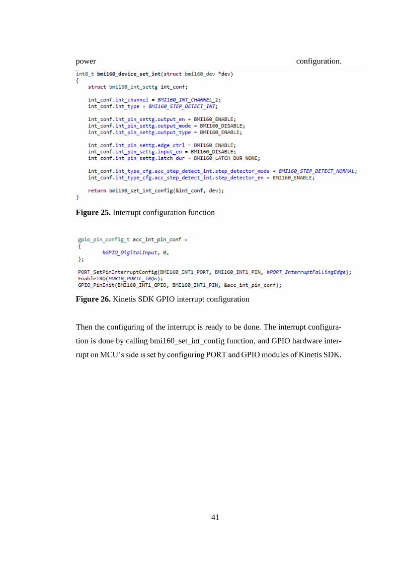
Figure 25. Interrupt configuration function p. 41
Figure 26. Kinetis SDK GPIO interrupt configuration p. 41
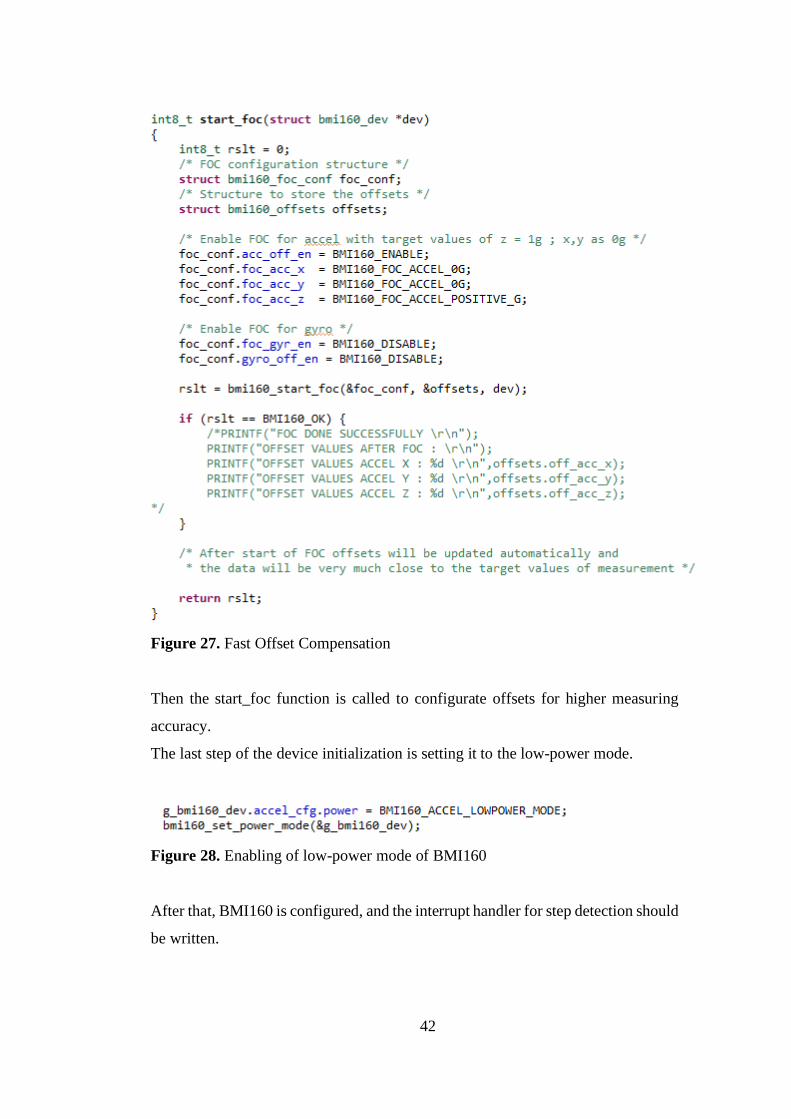
Figure 27. Fast Offset Compensation p. 42
Figure 28. Enabling of low-power mode of BMI160 p. 42
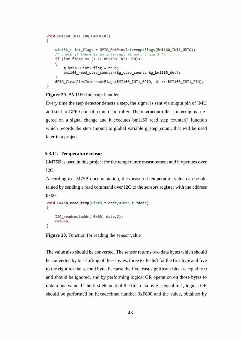
Figure 29. BMI160 Interrupt handler p. 43
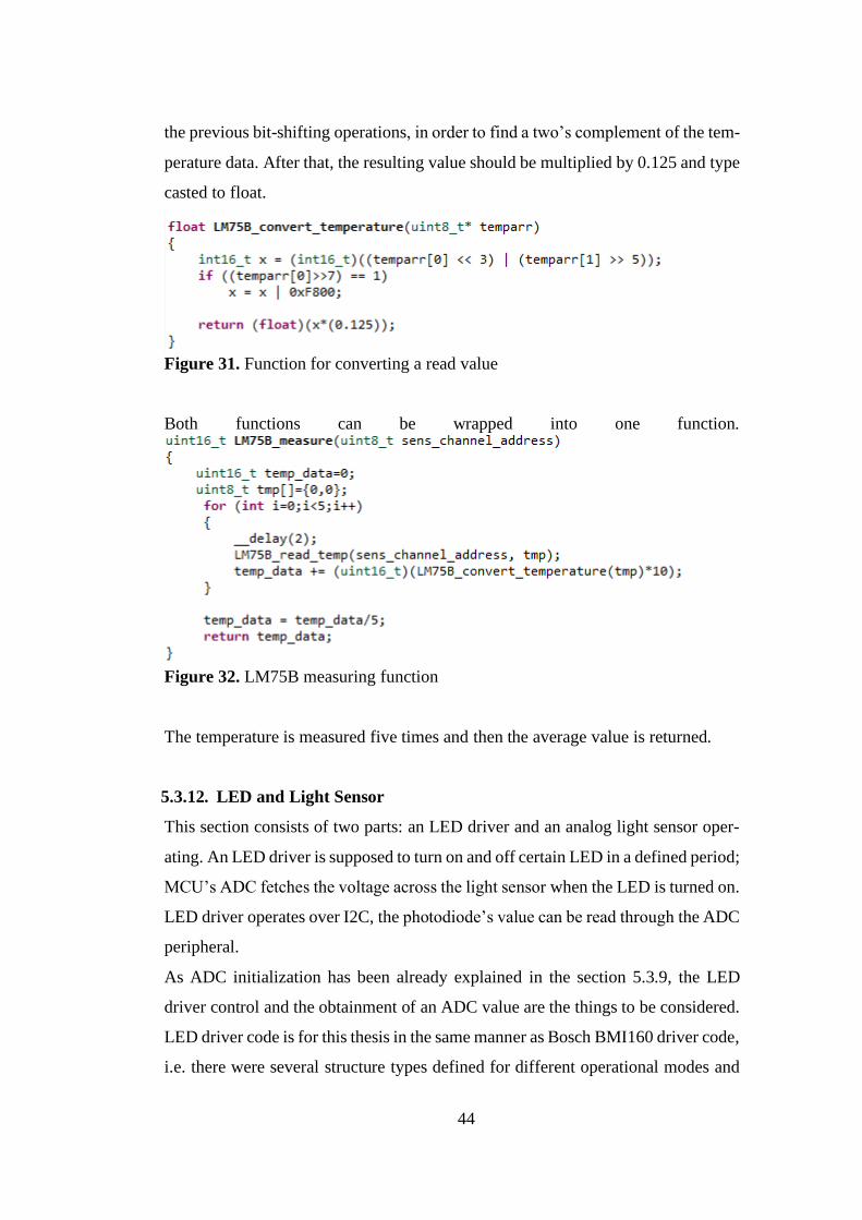
Figure 30. Function for reading the sensor value p. 43
Figure 31. Function for converting a read value p. 44
Figure 32. LM75B measuring function p. 44
Figure 33. Initialization of LTC3207 and SFH 2201 p. 45
Figure 34. Light measuring function p. 45
Figure 35. ltc3207_dev structure p. 46
Figure 36. LED_power function p. 46
Figure 37. ltc3207_set_uled function p. 47
Figure 38. Ring buffer structure p. 47
Figure 39. Ring buffer initialization function p. 47
Figure 40. Function for adding elements to a buffer p. 48
Figure 41. __fill_in_buff() p. 48
Figure 42. Function for obtaining elements from a buffer p. 48
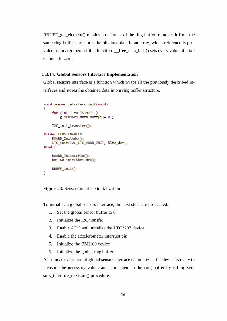
Figure 43. Sensors interface initialization p. 49
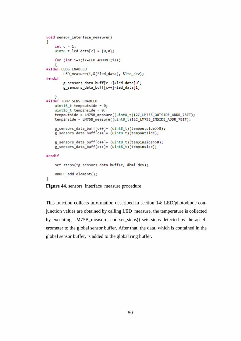
Figure 44. sensors_interface_measure procedure p. 50
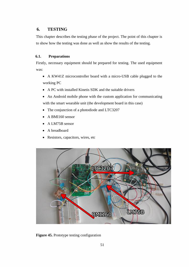
Figure 45. Prototype testing configuration p. 51
Table 1. GATT Services and Characteristics table p. 13

8
Table 2. Digital logic pin address defining p. 27

9
1. INTRODUCTION
Rapid growth and increasing accessibility of information technologies are changing
the way and the scope of application. Ubiquitous Internet access, low-power em-
bedded systems and powerful (in the way of performance) smartphones make it
possible to apply informational technologies on a personal level in many areas, in-
cluding the area of health monitoring. One of these applications of modern infor-
mation technologies is described in this thesis work: a compact health tracking de-
vice, which is designed in a form of a ring.
1.1. Delektre LTD
Delektre LTD is a small company placed in Vaasa, Finland. The company was
founded in 2010. The company offers research, consultancy and development ser-
vices for customers. The company cooperates with leading European research in-
stitutions and we are networked around the world from SMEs to conglomerates.
This company’s products include devices, such as a smart ring with exceptional
measurement capabilities.
Currently the company’s focus is on providing solutions in the sphere of healthcare.
/1/
1.2. Ring Development Background
A healthcare monitoring ring is a project which was started by Delektre in 2014.
The idea and the main features of this project were originated from the work of
Delektre and were based on a multispectral camera and the thesis work written by
Tommi Rintala /2/, which later was transformed into a personal health tracking ring
device. The first prototype of the ring was made by using Arduino Uno microcon-
troller board, which was later switched to Kinetis® KW41Z microcontroller due to
power saving options and better customization of the latter one.
1.3. Objective
The objective of this project is to produce a mobile, small-sized and low-power
embedded system which could be fit in a plastic case of a size of a ring, this includes
10
designing of embedded software and making an electronic scheme using a bread-
board and all selected components. As a result a fully working prototype of a system
should gather the data from the sensors, store it in a format of a ring buffer using
internal memory and transmit it over BLE connection in a pre-defined format.
1.4. Implementation plan
There are two distinct parts of a system that should be implemented: a software one
and a hardware one.
Software for the device must perform such functions as: Bluetooth functionality,
collecting data from different sensors and storing the obtained data. The application
is based on a BLE example application provided in Kinetis SDK where the func-
tionality has been already implemented partly; FreeRTOS used as a kernel for its
task management functionality.
A hardware element of a system consists of hardware selection (choosing the right
MCU and sensors) and designing electronic schematic with all necessary electronic
components. The list of all electronic components is provided by Delektre LTD.
11
2. THEORY AND BACKGROUND INFORMATION
The theory required to achieve the needed result, is introduced in this chapter.
2.1. Hardware
The hardware design of the prototype device consists of several parts: the micro-
controller board, an accelerometer, a temperature sensor, an LED driver and a pho-
tosensor, as well as resistors, capacitors and other components.
The microcontroller is the most important part of the project. It is required for the
project because of its ability to process, store and send information as well as to
operate sensors.
An accelerometer, temperature sensors, an LED driver and a photosensor are used
in the project to solve the specific task of the ring device. The purpose of these
components is described in the next section, 2.2.1.
2.2. Application Theory
This section contains theory of the measurements and the approach of their obtain-
ment, the application principles, the description of the BLE connection, the format
of the transmitted data and the method of storing obtained data.
2.2.1. Measurements
The theory behind measurements is to collect different type of data from different
sensors to analyse the health status of a person wearing the ring.
LEDs and a photodiode conjunction obtains a reflection of a LED light from the
skin of a finger. The principle of the work of these components is the same as pulse
oximetry. /3/ The photodiode changes voltage going through the diode, the change
in a voltage value has a linear relationship with illuminance: the more light is illu-
minated to a photodiode, the higher the voltage of a photodiode would be. The result
of the measurements is raw data of voltage values, produced by a photodiode by
reacting to different colour LED light reflection from the skin.
Two temperature sensors measure the temperature of human skin and the tempera-
ture outside the ring, the temperature of outside the ring is needed to bring more
accuracy to the measurements.
12
The amount of physical steps done by a user of a ring also plays part in the analysis
of the body state. An IMU with a step detecting feature is used for this purpose.
All data is sent as it is to the mobile phone application, where the data is sent to
other applications for detailed research and analysis.
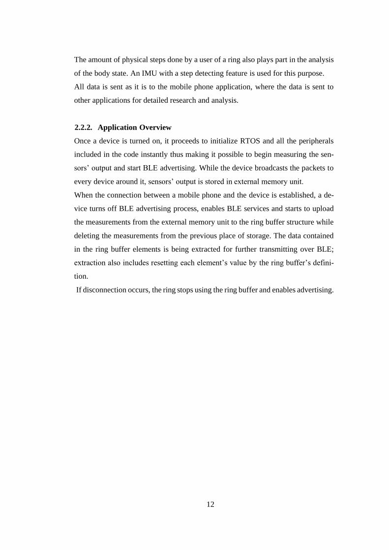
2.2.2. Application Overview
Once a device is turned on, it proceeds to initialize RTOS and all the peripherals
included in the code instantly thus making it possible to begin measuring the sen-
sors’ output and start BLE advertising. While the device broadcasts the packets to
every device around it, sensors’ output is stored in external memory unit.
When the connection between a mobile phone and the device is established, a de-
vice turns off BLE advertising process, enables BLE services and starts to upload
the measurements from the external memory unit to the ring buffer structure while
deleting the measurements from the previous place of storage. The data contained
in the ring buffer elements is being extracted for further transmitting over BLE;
extraction also includes resetting each element’s value by the ring buffer’s defini-
tion.
If disconnection occurs, the ring stops using the ring buffer and enables advertising.
13
Figure 1. Application diagram
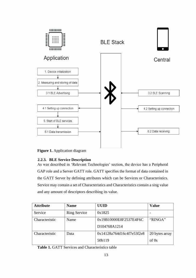
2.2.3. BLE Service Description
As was described in ‘Relevant Technologies’ section, the device has a Peripheral
GAP role and a Server GATT role. GATT specifies the format of data contained in
the GATT Server by defining attributes which can be Services or Characteristics.
Service may contain a set of Characteristics and Characteristics contain a sing value
and any amount of descriptors describing its value.
Attribute Name UUID Value
Service Ring Service 0x1825 -
Characteristic Name 0x19B10000E8F2537E4F6C
D104768A1214
“RINGA”
Characteristic Data 0x14128a764d16c4f7e53f2e8
50b119
20 bytes array
of 0s
Table 1. GATT Services and Characteristics table
14
The service is named “Ring Service” and has UUID 0x1825. The reason of choice
of such an UUID number was based on the lack of this number in GATT character-
istics list, provided by Bluetooth technology official website. /4/
This service contains two characteristics. The first one is “Name”, which has a value
of “RINGA” and specific UUID. This characteristic is used for discovering of the
ring device and can be read over the BLE connection. The second characteristic is
“Data”, which contains on empty 20 byte array filled with 0 values. This character-
istic is used for storing and transmitting the data gathered by the device and it can
be readable.
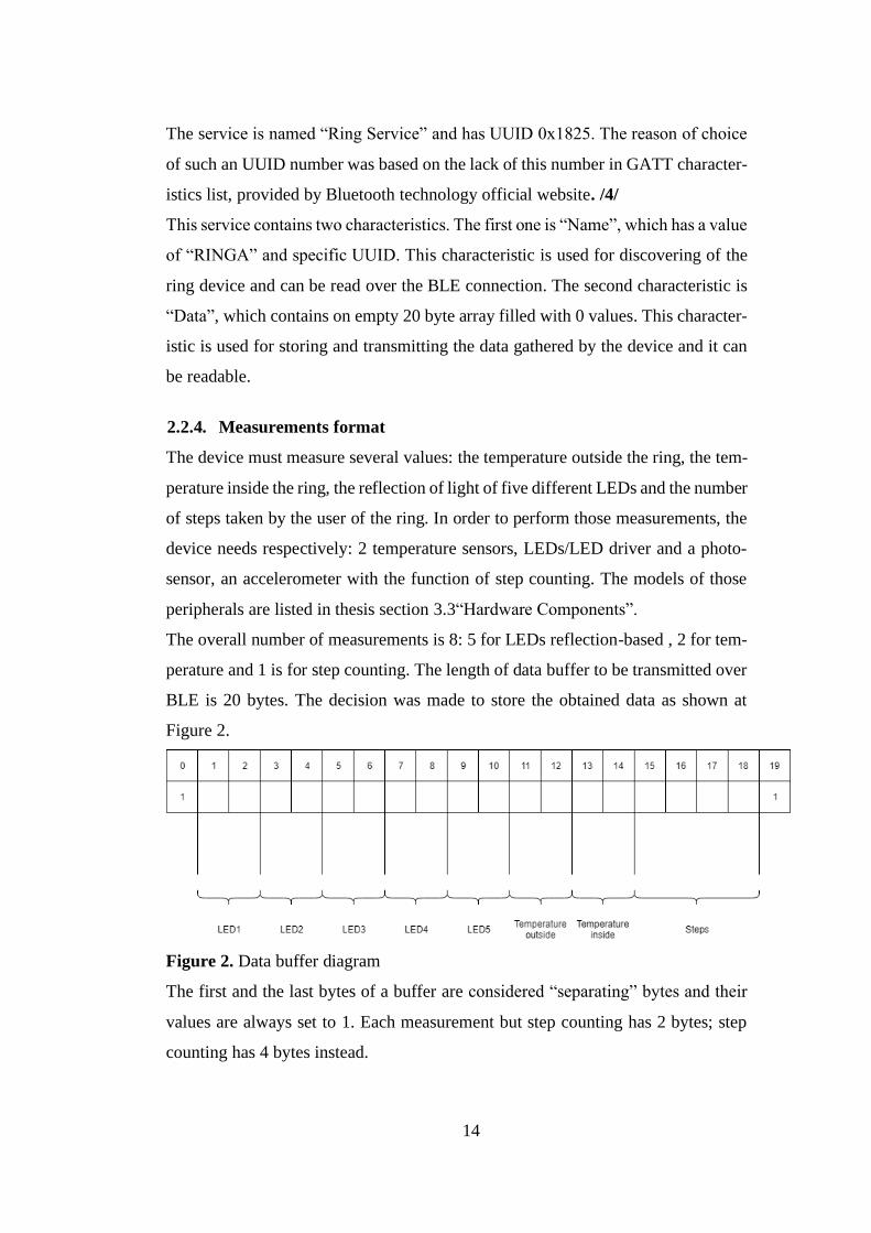
2.2.4. Measurements format
The device must measure several values: the temperature outside the ring, the tem-
perature inside the ring, the reflection of light of five different LEDs and the number
of steps taken by the user of the ring. In order to perform those measurements, the
device needs respectively: 2 temperature sensors, LEDs/LED driver and a photo-
sensor, an accelerometer with the function of step counting. The models of those
peripherals are listed in thesis section 3.3“Hardware Components”.
The overall number of measurements is 8: 5 for LEDs reflection-based , 2 for tem-
perature and 1 is for step counting. The length of data buffer to be transmitted over
BLE is 20 bytes. The decision was made to store the obtained data as shown at
Figure 2.
Figure 2. Data buffer diagram
The first and the last bytes of a buffer are considered “separating” bytes and their
values are always set to 1. Each measurement but step counting has 2 bytes; step
counting has 4 bytes instead.
15
Data received from the LEDs-photosensor system for each LED has a size of 12
bits. To transfer it over BLE, it should be stored in 2 bytes by putting 8 least signif-
icant bits to the second byte and the rest of the bits to the first byte.
Data of each temperature sensor is 2 bytes size, temperature data of each sensor is
split into two parts and is stored in each temperature sensor sector of BLE buffer.
The steps section of the BLE buffer allows to store up to 4 bytes, which means that
it is possible to store up to 4 294 967 295 steps, which is more than enough.
2.2.5. Ring buffer
Ring buffer is a data structure that uses a single fixed-size buffer as if it were con-
nected end-to-end. Due to the nature of a project, the ring buffer contains a single
array of arrays of 20 bytes; each array of 20 bytes has the same structure as a data
buffer described in Figure 2. The ring buffer is used in case when the connection
between the device and the mobile application is established; the data from the ex-
ternal unit is copied to ring buffer sub-array element and is deleted from the source.
With each operation on an element of the buffer, the tail and head pointers change
respectively.
16
3. USED TECHNOLOGY
The software tools and the hardware components of the project, which were se-
lected for the project implementation, are described in this chapter.
3.1. SDK
The software for the platform is created with the help of Kinetis SDK 2.0.
The MCUXpresso SDK is a comprehensive software enablement package designed
to simplify and accelerate application development with NXP’s LPC and Kinetis®
microcontrollers and i.MX RT crossover processors based on Arm® Cortex®-M
cores. The MCUXpresso SDK includes production-grade software with integrated
RTOS (optional), integrated stacks and middleware, reference software, and more.
/5/
3.2. Kernel
Amazon FreeRTOS™ is a kernel integrated into KSDK. It is a real-time operating
system, which extends the FreeRTOS kernel with several special related to Amazon
services features. /6/ /7/
FreeRTOS itself provides such features as:
• Pre-emptive or co-operative operation
• Flexible task priority assignment
• Flexible, fast and light task notification mechanism
• Queues
• Binary and counting semaphores
• Mutexes (including recursive mutexes)
• Software timers
• A tick-less capability
A full list of features can be found at Mastering the FreeRTOS Real Time Kernel
A Hands-On Tutorial Guide or at official FreeRTOS website.
3.2.1. KSDK Drivers and Modules Implementations
• Low Power Timer
17
• Analog-to-digital converter
• DCDC
• GPIO and PORT modules of MKW41Z
• I2C
• Bluetooth Low Energy
3.3. Hardware components
In order to make an embedded system application, one should know what type of
hardware is used, since the different electronical components are not easily replace-
able (both code-wise and connection-wise) and require different tools to be made
operative. In this section of the thesis, the list of components with their description
and explanation of their usage will be presented.
3.3.1. KW41Z MCU
The KW41Z is an ultra-low power, highly integrated single-chip device that enables
Bluetooth low energy (BLE), IEEE Std. 802.15.4 RF and Generic FSK connectivity
for portable, extremely low-power embedded systems.
The KW41Z SoC integrates a radio transceiver operating in the 2.36 GHz to 2.48
GHz range supporting a range of FSK/GFSK and O-QPSK modulations, an ARM
CortexM0+ CPU, up to 512 KB Flash and up to 128 KB SRAM, BLE Link Layer
hardware, 802.15.4 packet processor hardware and peripherals optimized to meet
the requirements of the target applications. /8/
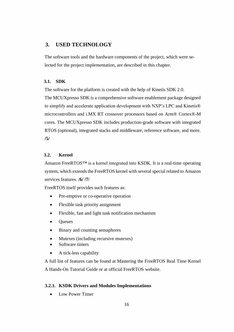
KW41Z is a core of the device. The KW41Z chip contains such functionality as
CPU, Flash, SRAM and peripherals. Software is executed on this chip and all hard-
ware components are connected to this chip. The used peripherals will be descripted
in detail in a software code chapter.
18
Figure 3. MKW41Z512VHT (source:nxp.com)
3.3.2. Crystal oscillator
Crystal oscillator is an electronic circuit used for generating a sinusoidal waveform
whose frequency is determined by piezoelectric crystal device. /9/
A crystal is a solid which consists of atoms, molecules or ions in a special order,
making a repeating pattern which extends in three dimensions. Usually the quartz
is used as a material for the crystal. /10/
The principle of operation of a crystal oscillator is to make a crystal of quartz dis-
torted by providing voltage to a nearby electrode or on the crystal itself creating an
electric field. After the electric field is removed, the crystal returns to its previous
form and generates voltage; the quartz behaviour is similar to the behaviour of RLC
circuit. As a result, resonant frequency is produced and can be used for purposes
described below.
The purpose of crystal oscillators is to provide stable clock signal for digital circuits
or to stabilize frequencies for radio transmitters and receivers by causing the fre-
quency which can be used as a reference for synchronizing.
There are two crystals in the device: one has 32 kHz frequency and another one has
32 MHz frequency.
The 32 kHz frequency crystal is used as a low power clock source for RTC periph-
eral, the 32 MHz frequency crystal is used as a clock for clocking MCU and Radio.
/11/
The chosen implementations of such components are FC-135 and FA-128 respec-
tively
19
Crystal oscillator is embedded into KW41Z microcontroller board.
3.3.3. LED Driver and LEDs
LEDs are used to produce light which will be reflected from the human skin. Due
to lack of digital-to-analog outputs in MKW41Z chip and for simplification of using
of LEDs, the LED driver is utilized. LTC3207 was chosen as a driver component.
LTC3207 has 8 pins to provide power to 8 LEDs and communicates through I2C
(or I²C). I2C stands for Inter-Integrated Circuit and it is a synchronous, multi-mas-
ter, multi-slave, single-ended serial bus. The driver has a role of slave in this bus,
while the MCU is in a master mode. The MCU sends commands over the bus to
turn LEDs on and off.
As the LED components for the purpose described in this section, the next compo-
nents were chosen: KINGBRIGHT 460nm-590nm APHB1608QBDSYKC, LU-
MEX 660nm LX0603SRW, LUMEX 636nm LX3632SISUGSBC, VISHAY
466nm TLMB1100, VISHAY 605nm VLMO1300, WURTH 850 nm
15406085BA300, WURTH 940nm 15406094BA500.
3.3.4. Photodiode
A photodiode is a semiconductor device that converts light into an electrical current
which is generated when photons are absorbed by a photodiode. SFH 2201 was
chosen as a photodiode component. The working mode of this photodiode is pho-
toconductive mode. The diode is reverse biased (cathode is driven positive with
respect to anode) and it reduces the response time by increasing the width of the
depletion region thus decreasing junction’s capacitance. The reverse bias also in-
creases dark current with small change in photocurrent.
The depletion region is the region in a semiconductor in which the mobile-carrier
charge density is insufficient to neutralize the net charge density of the fixed donor
and acceptor ions. /12/
Dark current is the relatively small electric current that flows through a photosen-
sitive device such as a photodiode even when no photons are entering the device; it
consists of the charges generated in the detector when no outside radiation is enter-
ing the detector.
20
3.3.5. Temperature Sensor
A temperature sensor is used to measure skin and outside temperatures. In this pro-
ject, the temperature-to-digital converter and temperature sensor LM75B is used.
This converter uses Sigma-Delta Analog-to-Digital conversion technique to convert
the signals from the sensors. The communication between MCU and this device
occurs with the help of I2C. /13/
3.3.6. IMU
Bosch BMI160 is a low-power IMU which has the features of accelerometer, gyro-
scope and externally connected device (magnetometer); nonetheless only the step
detecting function of an accelerometer is used. The communication between MCU
and this device occurs with the help of I2C. /14/
3.3.7. Resistors
Resistors in this project are commonly used to define output current in ICs or to
lower the voltage level.
3.3.8. Capacitors
Capacitors are used to filter the voltage peaks.
4. RELEVANT TECHNOLOGIES
In this section information on BLE and I2C technologies will be provided.
4.1. Bluetooth Low Energy (BLE)
The ring device is supposed to transfer the collected data to the phone application.
Bluetooth Low Energy technology satisfies such a requirement, as a Bluetooth chip-
set is a common module of modern smartphones.
The Bluetooth system defines a base profile which all devices implement. This pro-
file is called Generic Access Profile (GAP), which defines the basic requirements
and functionality. The GAP role of the project device is peripheral since the ring
responds to a phone application’s requests and it needs only one connection and
21
does not initiate a connection; the GAP role of mobile phone is central and it acts
as a master.
The Generic Attribute Profile (GATT) is built on top of Attribute Profile (ATT) and
it establishes operations and framework. GATT defines two roles: Server and Cli-
ent. In case of this project, the ring device acts as a GATT server since the device
accepts requests. The mobile phone application acts as a client respectively.
.
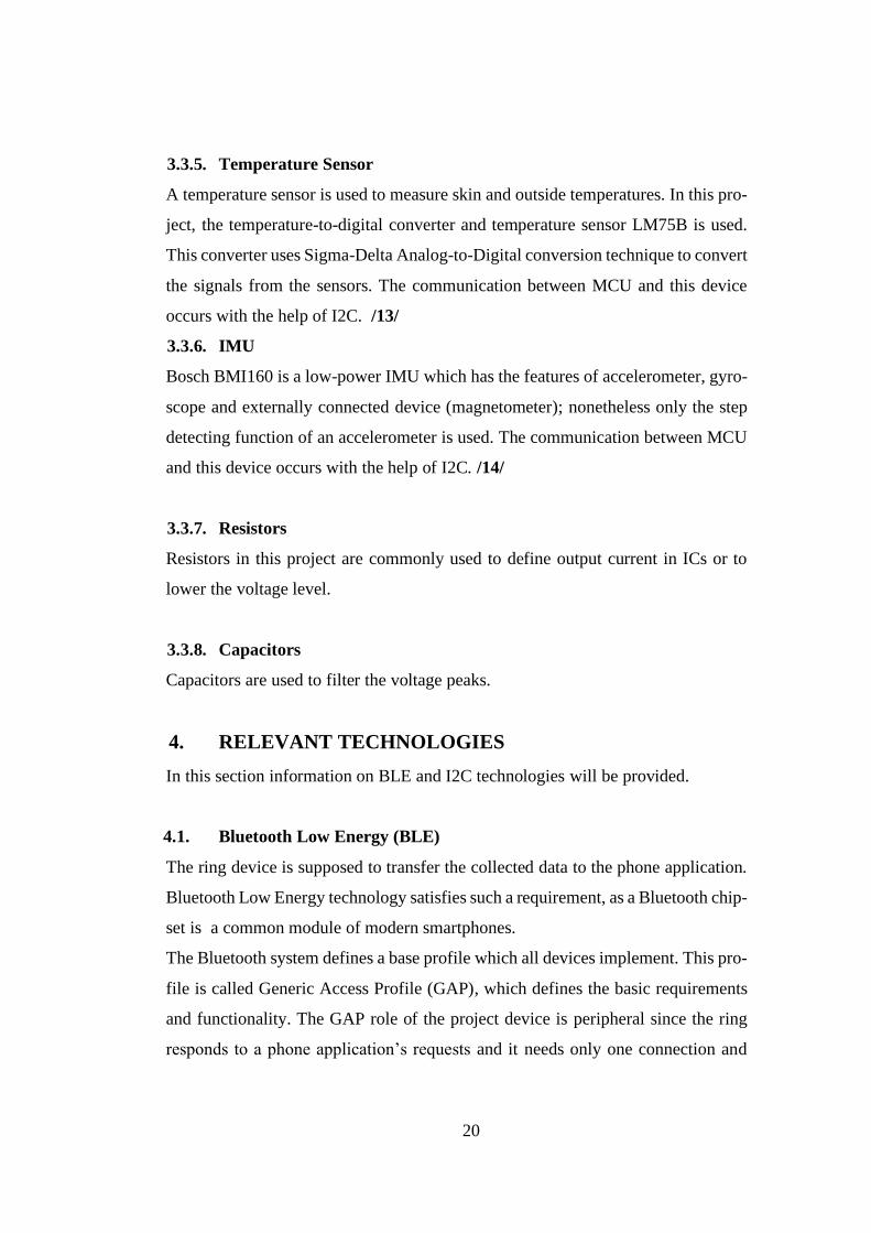
Figure 4. GATT-based Profile hierarchy (source: bluetooth.com)
In this project only one service is used; the service is primary and it provides the
characteristics of a ring device.
In this project the primary GATT service contains two characteristics: one is used
as a “device name”; this characteristic contains universal unique identifier (UUID)
value of a ring service with characteristics allowing GATT clients to read it and to
receive notifications. The second characteristic is “data characteristic” and this
characteristic is responsible for storing the data buffer which is sent over BLE later;
22
as well as the data buffer, the UUID of characteristic and the descriptor are defined
in this characteristic. The descriptor’s purpose is to specify either the server sends
notifications or indications; in case of this project, the notifications are sent over
BLE stream.
Since the Kinetis SDK provides all the necessary abstractions needed for all the
layers, no information on hardware specifications of Bluetooth technology will be
provided in this section.
4.2. I2C
I2C (Inter-Integrated Circuit) is a synchronous, multi-master, multi-slave, packet
switched, single-ended computer bus which is used for attaching lower-speed pe-
ripheral integrated circuits in intra-board communication. I2C is used in systems
where simplicity and low manufacturing cost are more important than communica-
tion speed. The main advantage of I2C is the capability of a processor or a micro-
controller to control the network of devices by using only 2 GPIO pins and software.
/15/
The ring device acts as a master to the components by generating the clock signal
and initiation the connection. The components BMI160 IMU, LM75B Temperature
sensor and LTC3207 LED Driver act as I2C slaves. All components are connected
to SDA and SCL lines with pull-up 10k Ohm resistors for each lane of each com-
ponent-to-bus connection. The transmission speed over I2C lines is set to 100
Kbit/s.

23
5. THE IMPLEMENTATION OF THE PROJECT
In this chapter the implementation and integration of hardware and software parts
of the project are set out.
5.1. Hardware Design Implementation
This chapter describes the hardware implementation of the prototype of this project.
The prototype is built of several components: Freescale Kinetis KW41Z MCU
board, Bosch BM160 IMU, LTC3207 LED driver, SFH2201 analog photodiode,
LM75B temperature sensor.
5.1.1. KW41Z MCU
Freescale Kinetis ® KW41Z MCU board is the core of the project. KW41Z can be
programmed to control all the connected modules, which are essential for this pro-
ject, as well as to store data obtained from the sensors.
The used features of KW41Z board are:
• BLE radio module
• I2C module
• ADC
• GPIO
5.1.2. LTC3207
LTC3207 is chosen as a LED driver for this project due to its low price and its
features, which are necessary to implement this project. These features of LTC3207
are:
• Up to 600 mA Total Output Current
• Independent On/Off, brightness level for each current source
• Ability to control LTC3207 by using 2-wire I2C interface
• Operating voltage: from 2.9V to 5.5V
5.1.3. SFH2201
SFH2201 was chosen as a photodiode. Notable features of SFH2201 are:
• It is an analog sensor, so no complicated interfaces needed
24
• Small package
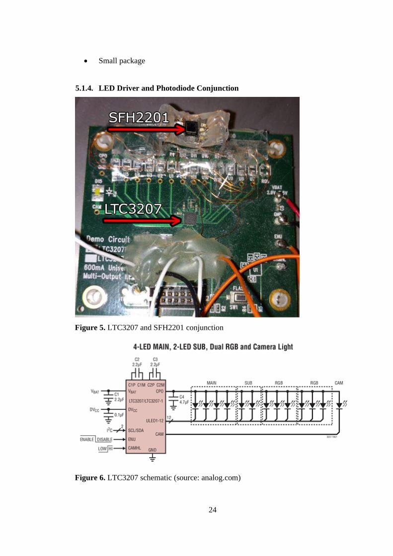
5.1.4. LED Driver and Photodiode Conjunction
Figure 5. LTC3207 and SFH2201 conjunction
Figure 6. LTC3207 schematic (source: analog.com)
25
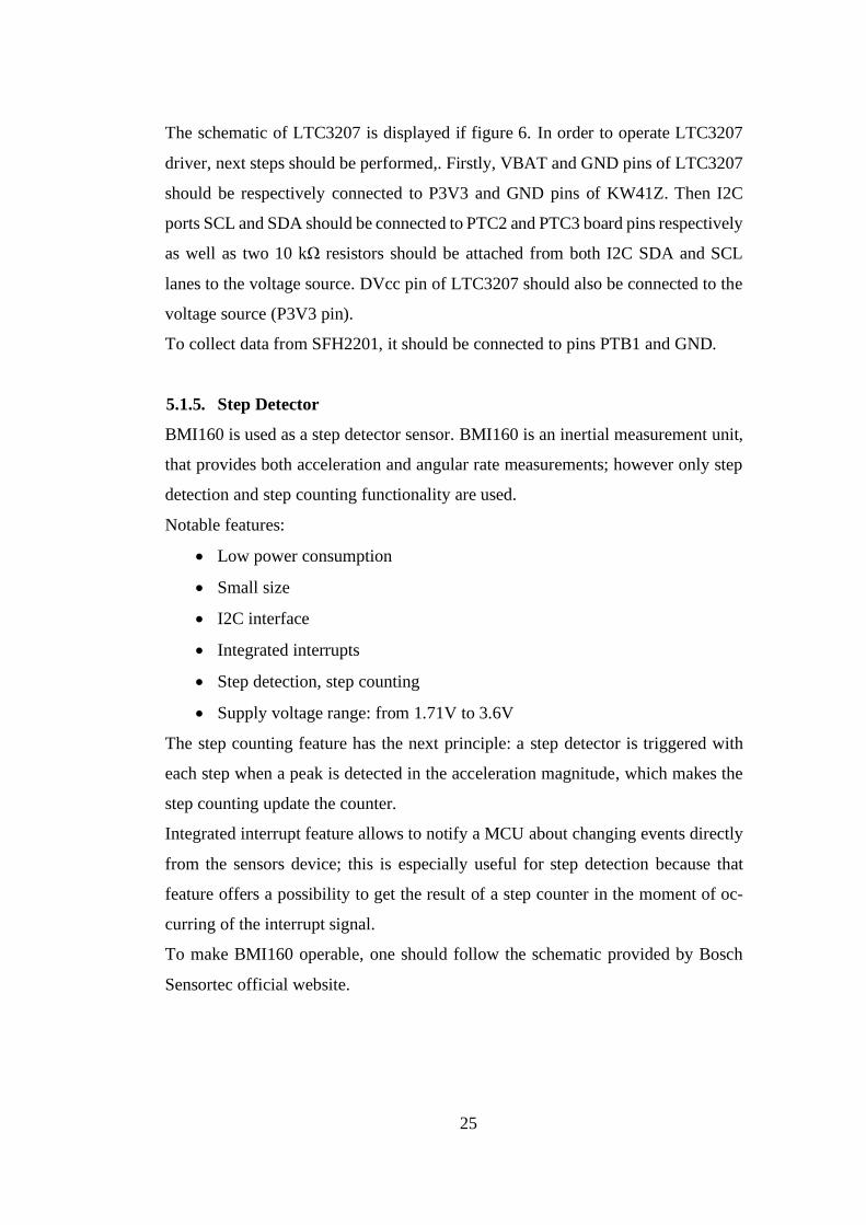
The schematic of LTC3207 is displayed if figure 6. In order to operate LTC3207
driver, next steps should be performed,. Firstly, VBAT and GND pins of LTC3207
should be respectively connected to P3V3 and GND pins of KW41Z. Then I2C
ports SCL and SDA should be connected to PTC2 and PTC3 board pins respectively
as well as two 10 kΩ resistors should be attached from both I2C SDA and SCL
lanes to the voltage source. DVcc pin of LTC3207 should also be connected to the
voltage source (P3V3 pin).
To collect data from SFH2201, it should be connected to pins PTB1 and GND.
5.1.5. Step Detector
BMI160 is used as a step detector sensor. BMI160 is an inertial measurement unit,
that provides both acceleration and angular rate measurements; however only step
detection and step counting functionality are used.
Notable features:
• Low power consumption
• Small size
• I2C interface
• Integrated interrupts
• Step detection, step counting
• Supply voltage range: from 1.71V to 3.6V
The step counting feature has the next principle: a step detector is triggered with
each step when a peak is detected in the acceleration magnitude, which makes the
step counting update the counter.
Integrated interrupt feature allows to notify a MCU about changing events directly
from the sensors device; this is especially useful for step detection because that
feature offers a possibility to get the result of a step counter in the moment of oc-
curring of the interrupt signal.
To make BMI160 operable, one should follow the schematic provided by Bosch
Sensortec official website.
26
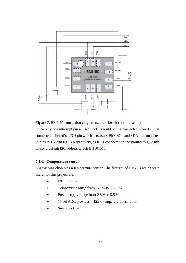
Figure 7. BMI160 connection diagram (source: bosch-sensortec.com)
Since only one interrupt pin is used, INT2 should not be connected when INT1 is
connected to board’s PTC5 pin which acts as a GPIO. SCL and SDA are connected
to pins PTC2 and PTC3 respectively, SDO is connected to the ground to give this
sensor a default I2C address which is 1101000.
5.1.6. Temperature sensor
LM75B was chosen as a temperature sensor. The features of LM75B which were
useful for this project are:
• I2C interface
• Temperature range from -55 ℃ to +125 ℃
• Power supply range from 2.8 V to 5.5 V
• 11-bit ADC provides 0.125℃ temperature resolution
• Small package
27
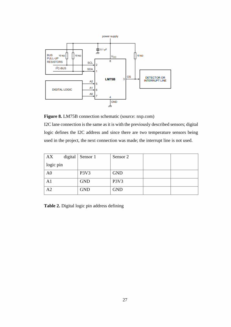
Figure 8. LM75B connection schematic (source: nxp.com)
I2C lane connection is the same as it is with the previously described sensors; digital
logic defines the I2C address and since there are two temperature sensors being
used in the project, the next connection was made; the interrupt line is not used.
AX digital
logic pin
Sensor 1 Sensor 2
A0 P3V3 GND
A1 GND P3V3
A2 GND GND
Table 2. Digital logic pin address defining
28
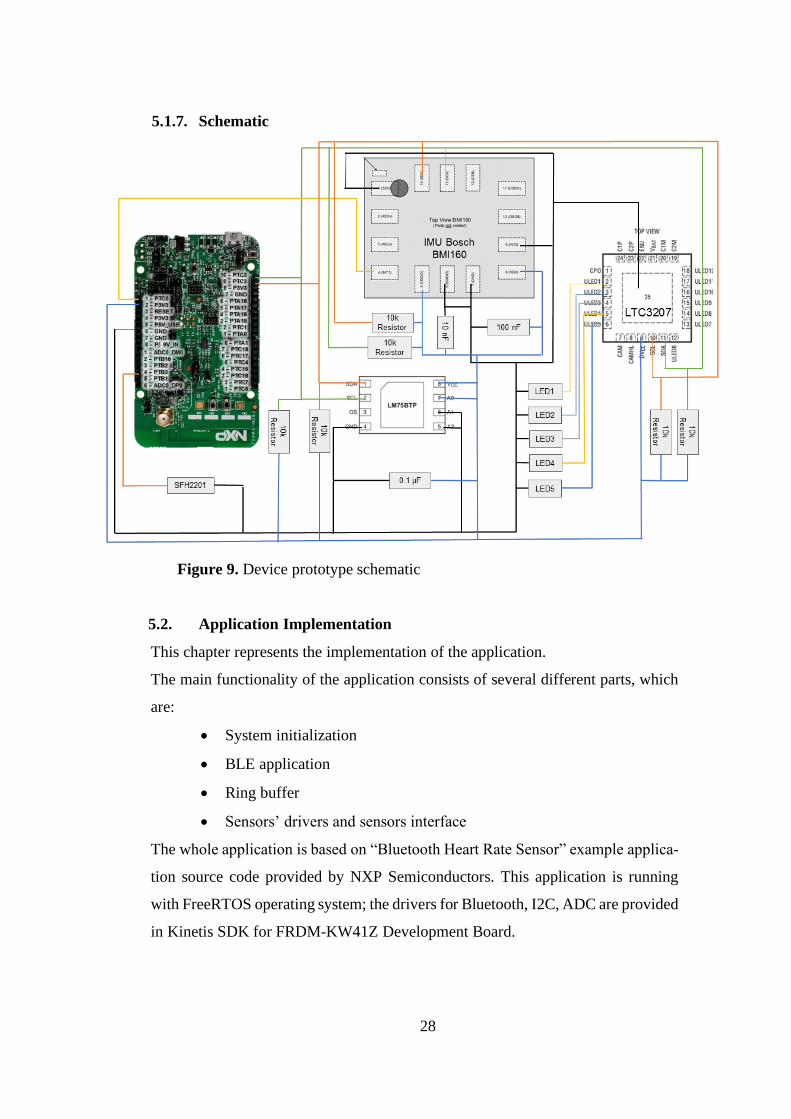
5.1.7. Schematic
Figure 9. Device prototype schematic
5.2. Application Implementation
This chapter represents the implementation of the application.
The main functionality of the application consists of several different parts, which
are:
• System initialization
• BLE application
• Ring buffer
• Sensors’ drivers and sensors interface
The whole application is based on “Bluetooth Heart Rate Sensor” example applica-
tion source code provided by NXP Semiconductors. This application is running
with FreeRTOS operating system; the drivers for Bluetooth, I2C, ADC are provided
in Kinetis SDK for FRDM-KW41Z Development Board.
29
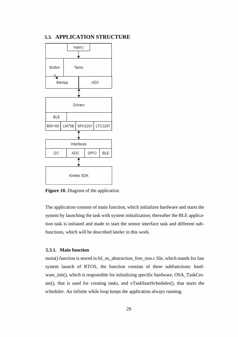
5.3. APPLICATION STRUCTURE
Figure 10. Diagram of the application
The application consists of main function, which initializes hardware and starts the
system by launching the task with system initialization; thereafter the BLE applica-
tion task is initiated and made to start the sensor interface task and different sub-
functions, which will be described lateler in this work.
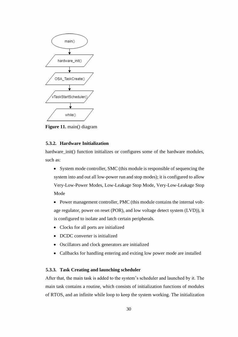
5.3.1. Main function
main() function is stored in fsl_os_abstraction_free_rtos.c file, which stands for fast
system launch of RTOS, the function consists of three subfunctions: hard-
ware_init(), which is responsible for initializing specific hardware, OSA_TaskCre-
ate(), that is used for creating tasks, and vTaskStartScheduler(), that starts the
scheduler. An infinite while loop keeps the application always running.
30
Figure 11. main() diagram
5.3.2. Hardware Initialization
hardware_init() function initializes or configures some of the hardware modules,
such as:
• System mode controller, SMC (this module is responsible of sequencing the
system into and out all low-power run and stop modes); it is configured to allow
Very-Low-Power Modes, Low-Leakage Stop Mode, Very-Low-Leakage Stop
Mode
• Power management controller, PMC (this module contains the internal volt-
age regulator, power on reset (POR), and low voltage detect system (LVD)), it
is configured to isolate and latch certain peripherals.
• Clocks for all ports are initialized
• DCDC converter is initialized
• Oscillators and clock generators are initialized
• Callbacks for handling entering and exiting low power mode are installed
5.3.3. Task Creating and launching scheduler
After that, the main task is added to the system’s scheduler and launched by it. The
main task contains a routine, which consists of initialization functions of modules
of RTOS, and an infinite while loop to keep the system working. The initialization
31
functions of modules of RTOS initialize message module private variables, timers,
LEDs, hardware cryptography, random module, non-volatile memory module,
modules for low-power operating mode and BLE application.
5.3.4. BLE Application
BLE Application consists of several functions:
• BleApp_init(), an initialization function of different peripherals
• BleApp_Start(), a start function which responds for starting advertising
• BleApp_HandleKeys(), a function for handling the buttons (board switches)
events (this feature is used in the prototype)
• BleApp_GenericCallback(), BLE Generic callback, which is responsible ei-
ther for configurating the BLE Stack by launching service after establishing a
connection between the device and a phone or by starting the advertisement
• BleApp_Config(), a configuration of BLE Stack is used for setting up the
advertisement, services, etc;
• BleApp_Advertise(), configuration and start of advertisement
• Callbacks for advertising, connection, GATT server, BleApp_Advertising-
Callback(), BleApp_ConnectionCallback() and BleApp_GattServerCallback()
• LocalTimeTickTimerCallback() and MeasurementsTimerCallback()
callback functions for a local timer and a measurement task timer
• UpdateMeasurementsTimerCallback() for a timed task for updating and up-
loading the measurements to internal memory
32
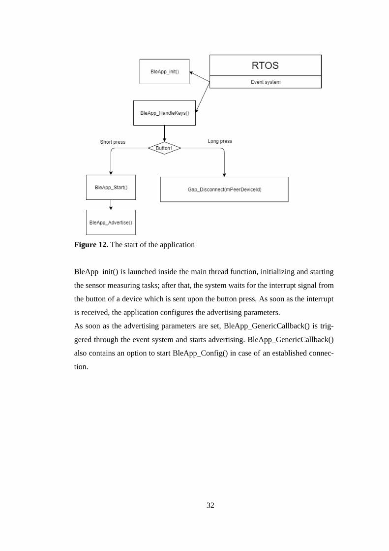
Figure 12. The start of the application
BleApp_init() is launched inside the main thread function, initializing and starting
the sensor measuring tasks; after that, the system waits for the interrupt signal from
the button of a device which is sent upon the button press. As soon as the interrupt
is received, the application configures the advertising parameters.
As soon as the advertising parameters are set, BleApp_GenericCallback() is trig-
gered through the event system and starts advertising. BleApp_GenericCallback()
also contains an option to start BleApp_Config() in case of an established connec-
tion.
33
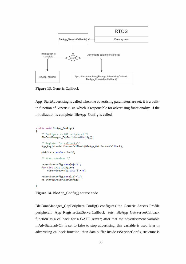
Figure 13. Generic Callback
App_StartAdvertising is called when the advertising parameters are set; it is a built-
in function of Kinetis SDK which is responsible for advertising functionality. If the
initialization is complete, BleApp_Config is called.
Figure 14. BleApp_Config() source code
BleConnManager_GapPeripheralConfig() configures the Generic Access Profile
peripheral; App_RegisterGattServerCallback sets BleApp_GattServerCallback
function as a callback for a GATT server; after that the advertisement variable
mAdvState.advOn is set to false to stop advertising, this variable is used later in
advertising callback function; then data buffer inside rsServiceConfig structure is
34
set to its default value and starts “Ring Service” by launching Rs_Start function
with the reference to the service configuration structure as an argument.
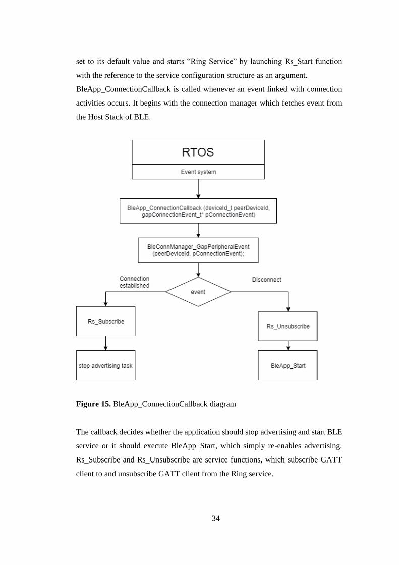
BleApp_ConnectionCallback is called whenever an event linked with connection
activities occurs. It begins with the connection manager which fetches event from
the Host Stack of BLE.
Figure 15. BleApp_ConnectionCallback diagram
The callback decides whether the application should stop advertising and start BLE
service or it should execute BleApp_Start, which simply re-enables advertising.
Rs_Subscribe and Rs_Unsubscribe are service functions, which subscribe GATT
client to and unsubscribe GATT client from the Ring service.
35
5.3.5. GATT Profile
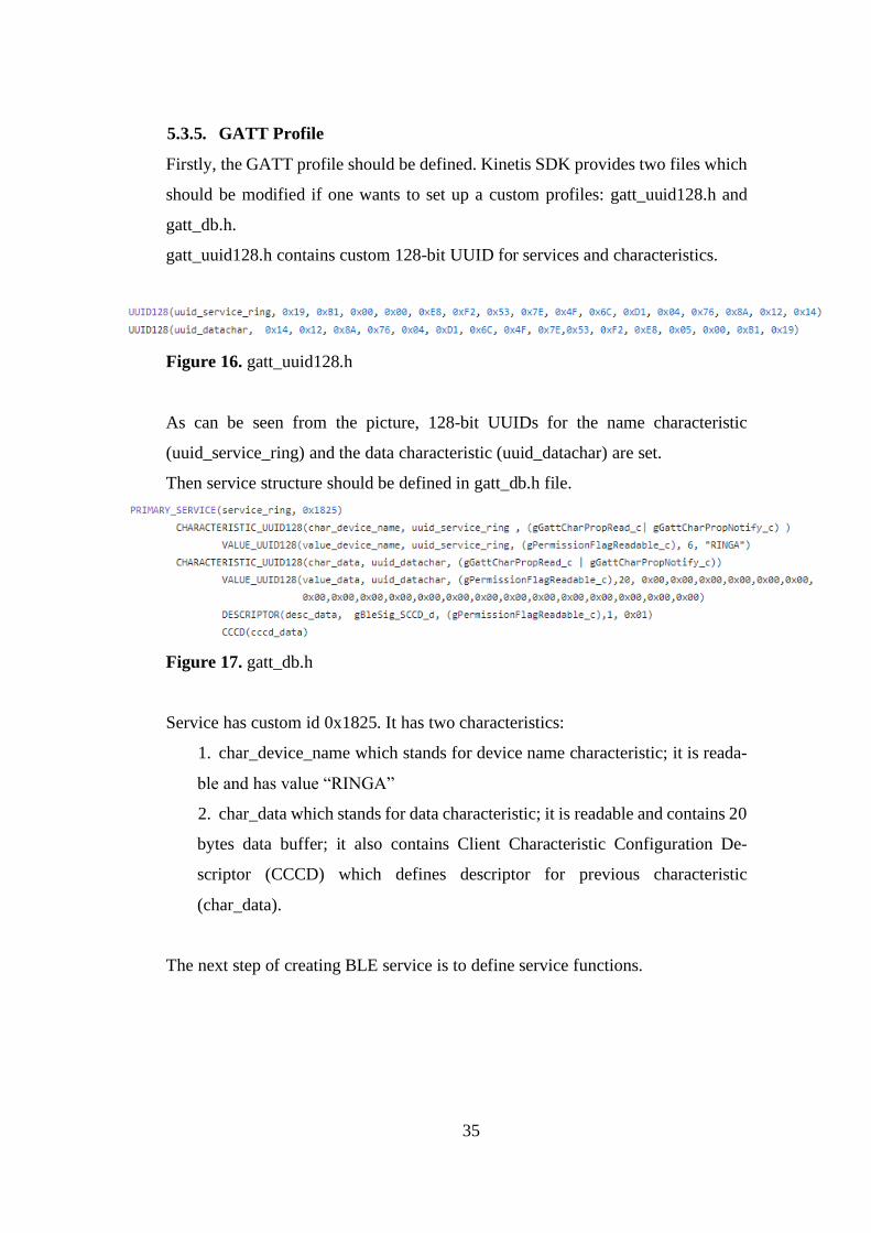
Firstly, the GATT profile should be defined. Kinetis SDK provides two files which
should be modified if one wants to set up a custom profiles: gatt_uuid128.h and
gatt_db.h.
gatt_uuid128.h contains custom 128-bit UUID for services and characteristics.
Figure 16. gatt_uuid128.h
As can be seen from the picture, 128-bit UUIDs for the name characteristic
(uuid_service_ring) and the data characteristic (uuid_datachar) are set.
Then service structure should be defined in gatt_db.h file.
Figure 17. gatt_db.h
Service has custom id 0x1825. It has two characteristics:
1. char_device_name which stands for device name characteristic; it is reada-
ble and has value “RINGA”
2. char_data which stands for data characteristic; it is readable and contains 20
bytes data buffer; it also contains Client Characteristic Configuration De-
scriptor (CCCD) which defines descriptor for previous characteristic
(char_data).
The next step of creating BLE service is to define service functions.
36
5.3.6. BLE Service Functions
Once the GATT profile is configured, drivers are required to handle and to respond
to client’s requests properly. Two files were created: ring_service.c and ring_inter-
face.h. ring_interface.h consists definitions of functions and data types required for
the service functionality; ring_service.c contains service functions.
Functions:
• bleResult_t Rs_Start(rsConfig_t *rServiceConfig) – start service
• bleResult_t Rs_Stop(rsConfig_t *rServiceConfig) = stop service
• bleResult_t Rs_Subscribe(deviceId_t clientDeviceId) – subscribe a specific
client to a service
• bleResult_t Rs_Unsubscribe() – unsubscribe a specific client from a service
• bleResult_t Rs_SetService(uint16_t handle, uint8_t* data) – writes data
characteristic and invokes Rs_SendDataNotification
• bleResult_t Rs_RecordData(uint16_t serviceHandle, uint8_t* data) – writes
data to GATT database making it possible to obtain the data by client
• void Rs_SendDataNotification(uint16_t serviceHandle) – send notification
to a client
Data types:
• struct rsConfig_tag, which is also redefined as rsConfig_t
• bleResult_t is pre-defined enum variable type with values for different out-
comes
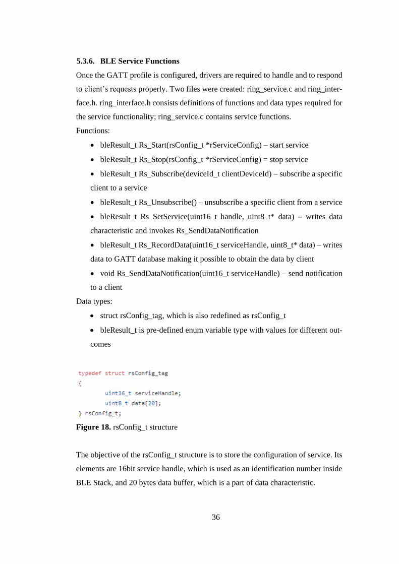
Figure 18. rsConfig_t structure
The objective of the rsConfig_t structure is to store the configuration of service. Its
elements are 16bit service handle, which is used as an identification number inside
BLE Stack, and 20 bytes data buffer, which is a part of data characteristic.
37
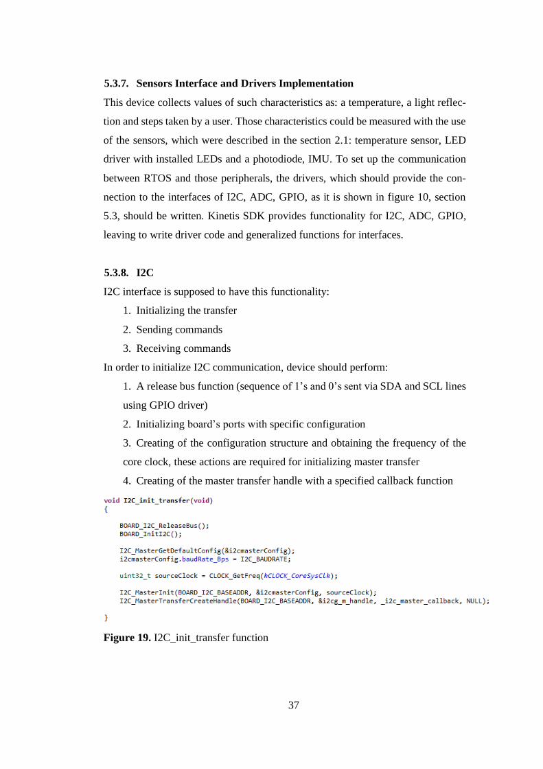
5.3.7. Sensors Interface and Drivers Implementation
This device collects values of such characteristics as: a temperature, a light reflec-
tion and steps taken by a user. Those characteristics could be measured with the use
of the sensors, which were described in the section 2.1: temperature sensor, LED
driver with installed LEDs and a photodiode, IMU. To set up the communication
between RTOS and those peripherals, the drivers, which should provide the con-
nection to the interfaces of I2C, ADC, GPIO, as it is shown in figure 10, section
5.3, should be written. Kinetis SDK provides functionality for I2C, ADC, GPIO,
leaving to write driver code and generalized functions for interfaces.
5.3.8. I2C
I2C interface is supposed to have this functionality:
1. Initializing the transfer
2. Sending commands
3. Receiving commands
In order to initialize I2C communication, device should perform:
1. A release bus function (sequence of 1’s and 0’s sent via SDA and SCL lines
using GPIO driver)
2. Initializing board’s ports with specific configuration
3. Creating of the configuration structure and obtaining the frequency of the
core clock, these actions are required for initializing master transfer
4. Creating of the master transfer handle with a specified callback function
Figure 19. I2C_init_transfer function
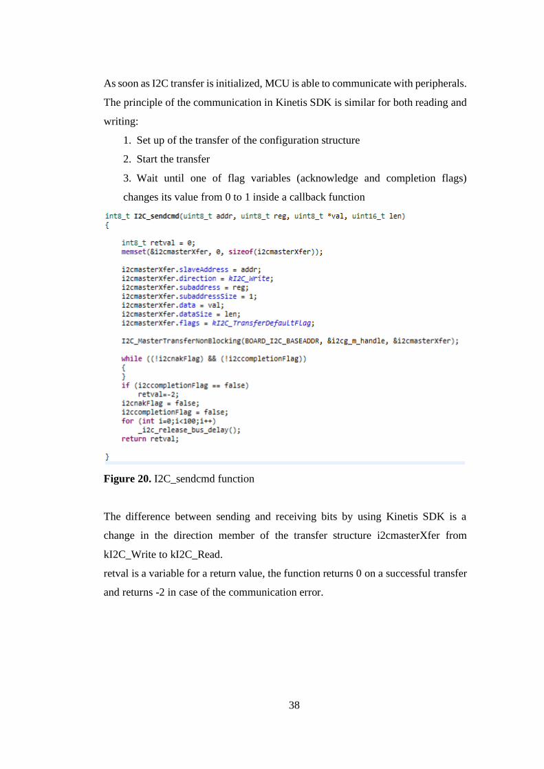
38
As soon as I2C transfer is initialized, MCU is able to communicate with peripherals.
The principle of the communication in Kinetis SDK is similar for both reading and
writing:
1. Set up of the transfer of the configuration structure
2. Start the transfer
3. Wait until one of flag variables (acknowledge and completion flags)
changes its value from 0 to 1 inside a callback function
Figure 20. I2C_sendcmd function
The difference between sending and receiving bits by using Kinetis SDK is a
change in the direction member of the transfer structure i2cmasterXfer from
kI2C_Write to kI2C_Read.
retval is a variable for a return value, the function returns 0 on a successful transfer
and returns -2 in case of the communication error.
39
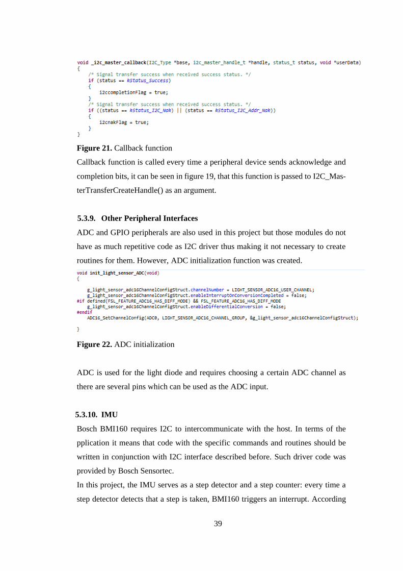
Figure 21. Callback function
Callback function is called every time a peripheral device sends acknowledge and
completion bits, it can be seen in figure 19, that this function is passed to I2C_Mas-
terTransferCreateHandle() as an argument.
5.3.9. Other Peripheral Interfaces
ADC and GPIO peripherals are also used in this project but those modules do not
have as much repetitive code as I2C driver thus making it not necessary to create
routines for them. However, ADC initialization function was created.
Figure 22. ADC initialization
ADC is used for the light diode and requires choosing a certain ADC channel as
there are several pins which can be used as the ADC input.
5.3.10. IMU
Bosch BMI160 requires I2C to intercommunicate with the host. In terms of the
pplication it means that code with the specific commands and routines should be
written in conjunction with I2C interface described before. Such driver code was
provided by Bosch Sensortec.
In this project, the IMU serves as a step detector and a step counter: every time a
step detector detects that a step is taken, BMI160 triggers an interrupt. According
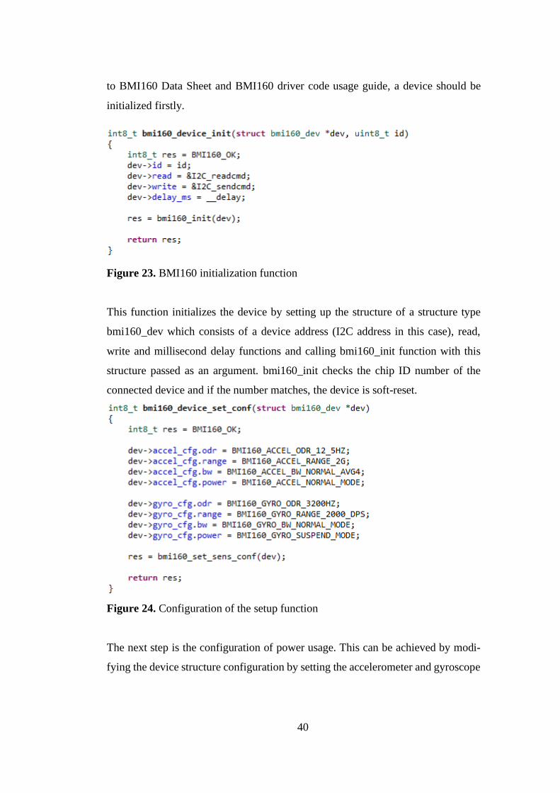
40
to BMI160 Data Sheet and BMI160 driver code usage guide, a device should be
initialized firstly.
Figure 23. BMI160 initialization function
This function initializes the device by setting up the structure of a structure type
bmi160_dev which consists of a device address (I2C address in this case), read,
write and millisecond delay functions and calling bmi160_init function with this
structure passed as an argument. bmi160_init checks the chip ID number of the
connected device and if the number matches, the device is soft-reset.
Figure 24. Configuration of the setup function
The next step is the configuration of power usage. This can be achieved by modi-
fying the device structure configuration by setting the accelerometer and gyroscope
41
power configuration.
Figure 25. Interrupt configuration function
Figure 26. Kinetis SDK GPIO interrupt configuration
Then the configuring of the interrupt is ready to be done. The interrupt configura-
tion is done by calling bmi160_set_int_config function, and GPIO hardware inter-
rupt on MCU’s side is set by configuring PORT and GPIO modules of Kinetis SDK.
42
Figure 27. Fast Offset Compensation
Then the start_foc function is called to configurate offsets for higher measuring
accuracy.
The last step of the device initialization is setting it to the low-power mode.
Figure 28. Enabling of low-power mode of BMI160
After that, BMI160 is configured, and the interrupt handler for step detection should
be written.
43
Figure 29. BMI160 Interrupt handler
Every time the step detector detects a step, the signal is sent via output pin of IMU
and sent to GPIO port of a microcontroller. The microcontroller’s interrupt is trig-
gered on a signal change and it executes bmi160_read_step_counter() function
which records the step amount to global variable g_step_count, that will be used
later in a project.
5.3.11. Temperature sensor
LM75B is used in this project for the temperature measurement and it operates over
I2C.
According to LM75B documentation, the measured temperature value can be ob-
tained by sending a read command over I2C to the sensors register with the address
0x00.
Figure 30. Function for reading the sensor value
The value also should be converted. The sensor returns two data bytes which should
be converted by bit-shifting of these bytes, three to the left for the first byte and five
to the right for the second byte, because the five least significant bits are equal to 0
and should be ignored, and by performing logical OR operation on those bytes to
obtain one value. If the first element of the first data byte is equal to 1, logical OR
should be performed on hexadecimal number 0xF800 and the value, obtained by
44
the previous bit-shifting operations, in order to find a two’s complement of the tem-
perature data. After that, the resulting value should be multiplied by 0.125 and type
casted to float.
Figure 31. Function for converting a read value
Both functions can be wrapped into one function.
Figure 32. LM75B measuring function
The temperature is measured five times and then the average value is returned.
5.3.12. LED and Light Sensor
This section consists of two parts: an LED driver and an analog light sensor oper-
ating. An LED driver is supposed to turn on and off certain LED in a defined period;
MCU’s ADC fetches the voltage across the light sensor when the LED is turned on.
LED driver operates over I2C, the photodiode’s value can be read through the ADC
peripheral.
As ADC initialization has been already explained in the section 5.3.9, the LED
driver control and the obtainment of an ADC value are the things to be considered.
LED driver code is for this thesis in the same manner as Bosch BMI160 driver code,
i.e. there were several structure types defined for different operational modes and
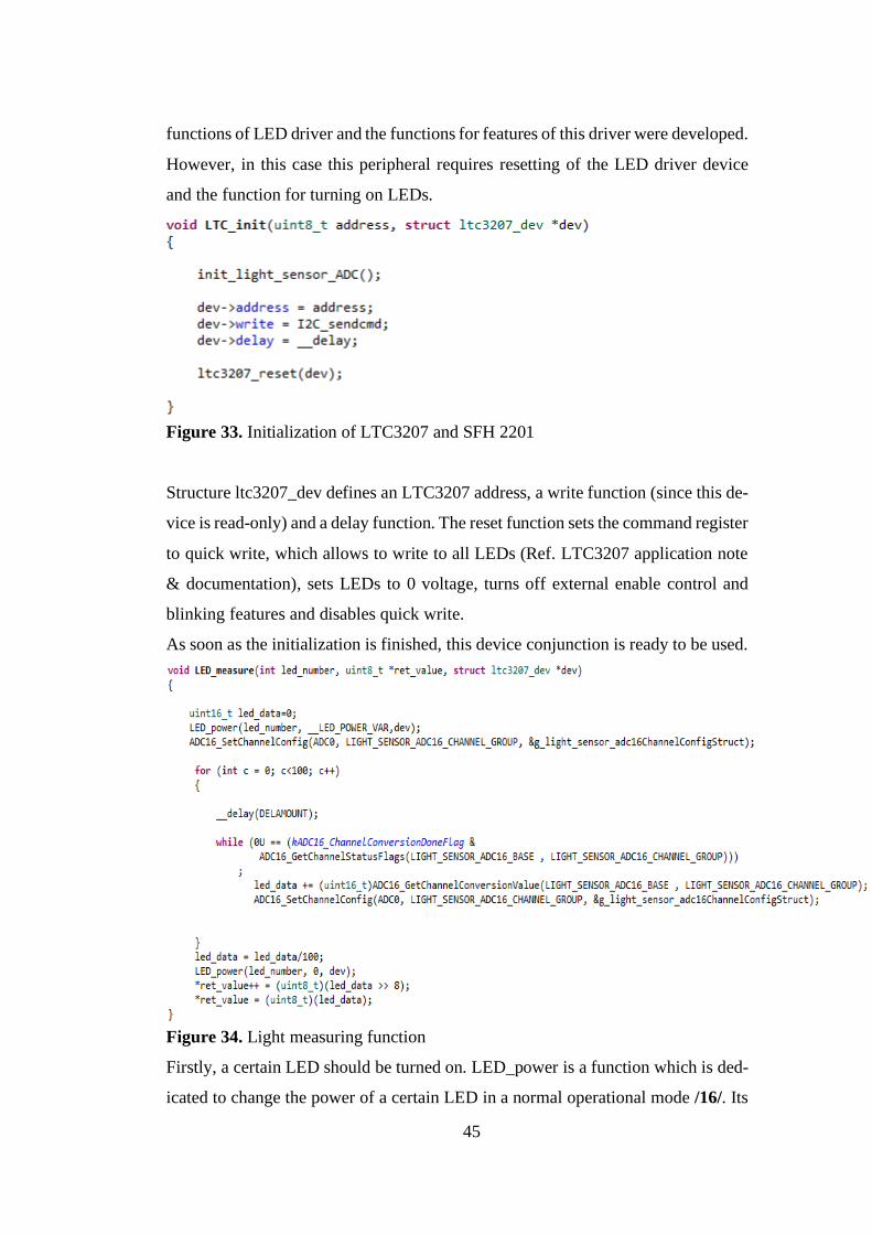
45
functions of LED driver and the functions for features of this driver were developed.
However, in this case this peripheral requires resetting of the LED driver device
and the function for turning on LEDs.
Figure 33. Initialization of LTC3207 and SFH 2201
Structure ltc3207_dev defines an LTC3207 address, a write function (since this de-
vice is read-only) and a delay function. The reset function sets the command register
to quick write, which allows to write to all LEDs (Ref. LTC3207 application note
& documentation), sets LEDs to 0 voltage, turns off external enable control and
blinking features and disables quick write.
As soon as the initialization is finished, this device conjunction is ready to be used.
Figure 34. Light measuring function
Firstly, a certain LED should be turned on. LED_power is a function which is ded-
icated to change the power of a certain LED in a normal operational mode /16/. Its
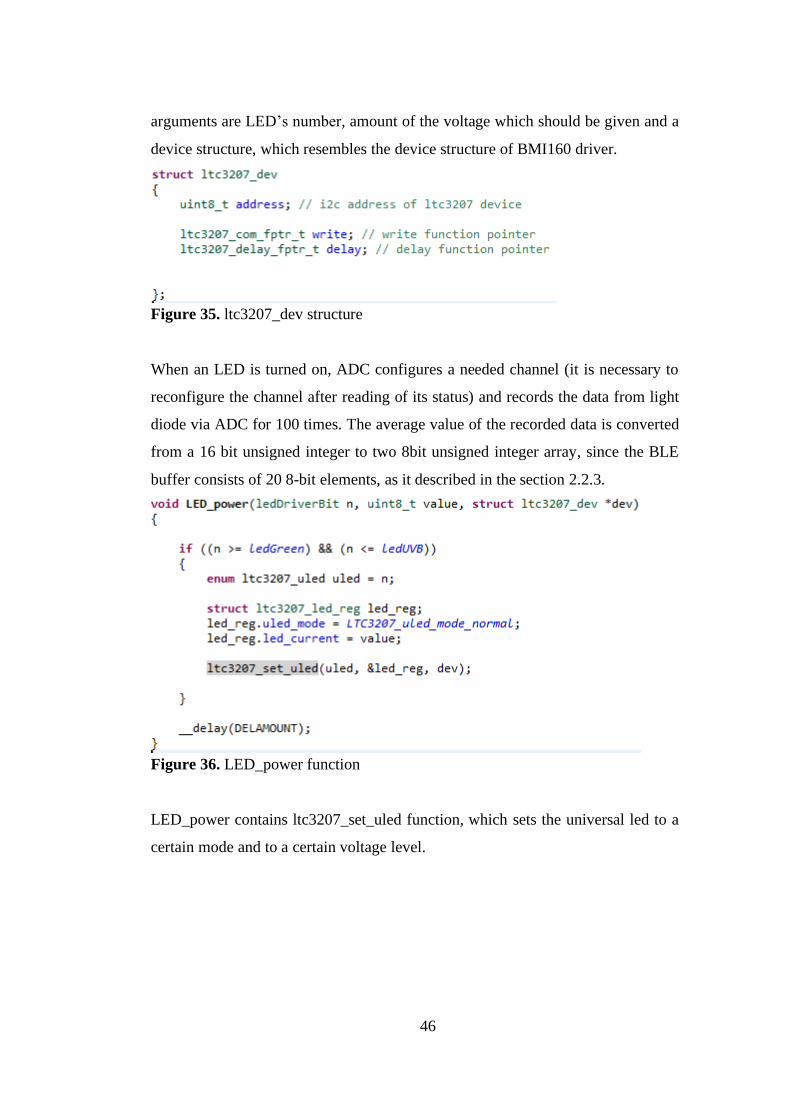
46
arguments are LED’s number, amount of the voltage which should be given and a
device structure, which resembles the device structure of BMI160 driver.
Figure 35. ltc3207_dev structure
When an LED is turned on, ADC configures a needed channel (it is necessary to
reconfigure the channel after reading of its status) and records the data from light
diode via ADC for 100 times. The average value of the recorded data is converted
from a 16 bit unsigned integer to two 8bit unsigned integer array, since the BLE
buffer consists of 20 8-bit elements, as it described in the section 2.2.3.
Figure 36. LED_power function
LED_power contains ltc3207_set_uled function, which sets the universal led to a
certain mode and to a certain voltage level.
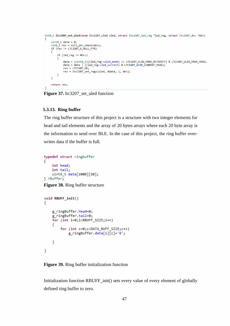
47
Figure 37. ltc3207_set_uled function
5.3.13. Ring buffer
The ring buffer structure of this project is a structure with two integer elements for
head and tail elements and the array of 20 bytes arrays where each 20 byte array is
the information to send over BLE. In the case of this project, the ring buffer over-
writes data if the buffer is full.
Figure 38. Ring buffer structure
Figure 39. Ring buffer initialization function
Initialization function RBUFF_init() sets every value of every element of globally
defined ring buffer to zero.
48
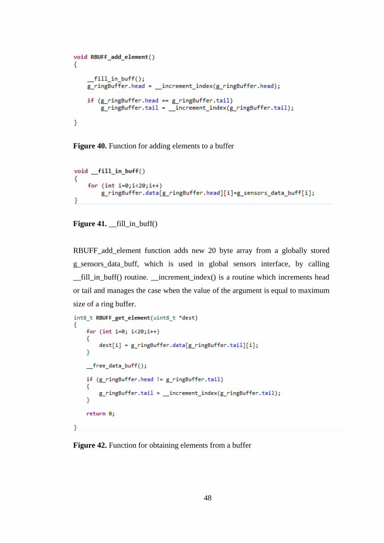
Figure 40. Function for adding elements to a buffer
Figure 41. __fill_in_buff()
RBUFF_add_element function adds new 20 byte array from a globally stored
g_sensors_data_buff, which is used in global sensors interface, by calling
__fill_in_buff() routine. __increment_index() is a routine which increments head
or tail and manages the case when the value of the argument is equal to maximum
size of a ring buffer.
Figure 42. Function for obtaining elements from a buffer
49
RBUFF_get_element() obtains an element of the ring buffer, removes it from the
same ring buffer and stores the obtained data in an array, which reference is pro-
vided as an argument of this function. __free_data_buff() sets every value of a tail
element to zero.
5.3.14. Global Sensors Interface Implementation
Global sensors interface is a function which wraps all the previously described in-
terfaces and stores the obtained data into a ring buffer structure.
Figure 43. Sensors interface initialization
To initialize a global sensors interface, the next steps are proceeded:
1. Set the global sensor buffer to 0
2. Initialize the I2C transfer
3. Enable ADC and initialize the LTC3207 device
4. Enable the accelerometer interrupt pin
5. Initialize the BMI160 device
6. Initialize the global ring buffer
As soon as every part of global sensor interface is initialized, the device is ready to
measure the necessary values and store them in the ring buffer by calling sen-
sors_interface_measure() procedure.
50
Figure 44. sensors_interface_measure procedure
This function collects information described in section 14: LED/photodiode con-
junction values are obtained by calling LED_measure, the temperature is collected
by executing LM75B_measure, and set_steps() sets steps detected by the accel-
erometer to the global sensor buffer. After that, the data, which is contained in the
global sensor buffer, is added to the global ring buffer.
51
6. TESTING
This chapter describes the testing phase of the project. The point of this chapter is
to show how the testing was done as well as show the results of the testing.
6.1. Preparations
Firstly, necessary equipment should be prepared for testing. The used equipment
was:
• A KW41Z microcontroller board with a micro-USB cable plugged to the
working PC
• A PC with installed Kinetis SDK and the suitable drivers
• An Android mobile phone with the custom application for communicating
with the smart wearable unit (the development board in this case)
• The conjunction of a photodiode and LTC3207
• A BMI160 sensor
• A LM75B sensor
• A breadboard
• Resistors, capacitors, wires, etc
Figure 45. Prototype testing configuration
52
Secondly, all of the components were connected to the microcontroller board the
way it was described in section 5.1. Each of the sensors is connected to the common
ground and to the common voltage source (GND and P3V3 board pins); each sensor
having I2C is connected to I2C lanes leading to PTC2 and PTC3 and each of I2C
connection has a pull up resistor to the voltage source.
Thirdly, MCUXpresso software with installed Kinetis SDK was run and the firm-
ware for a wearable unit was loaded to the board.
After every connection was made and the firmware was loaded, the microprocessor
started the program, the LED driver started lighting up LEDs in certain order, sen-
sors started measuring necessary data and the BLE module started advertising.
6.2. Testing phase
The testing phase has several stages. The first stage is a test of BLE connection
between microcontroller board and the mobile phone application. During this stage,
the buffer containing 1XXX XXXX XXXX XXXX XXX1 bytes, where X is either
1 or 0, was sent to the mobile phone periodically. As soon as the mobile application
started to correctly receive packages, the testing process moved to the next stage.
The second stage of testing is to check the microcontroller’s ability of obtaining the
data from sensors. In order to proceed this testing step, the source code for each
module (the LED driver and light sensor conjunction, the temperature sensor, the
accelerometer source code) was carried out to separate projects and was tested in-
dividually. After completing this stage, the testing of functionality of the ring buffer
was performed.
During the third of stage, the ring buffer was made to gather and to remove (push
and pop operations) random data periodically. When the ring buffer successfully
performed processing of incoming and outcoming data, the testing phase moved to
the last step of the complete testing of the system.
The objective of this step is to make each part of the project work with the other
parts. The source code of the sensors and the ring buffer was integrated into the
BLE source code. The sensors successfully obtained data and passed it to the board;
the ring buffer interface was able to store in and return data from the ring buffer;

53
finally, the BLE connection between the board and the application was established
and the data was correctly sent via a Bluetooth connection.
The whole testing went successfully, and the project was made to operate as desired
without any flaws: the sensor data was gathered, stored and sent over a Bluetooth
connection. The mobile phone application received exactly the same information
the microcontroller board sent to it.

54
7. CONCLUSION AND FUTURE WORK
In this thesis project, the prototype of a device was built and the software for that
device was written to provide the base for a mobile health-monitoring skin-analyz-
ing device as a solution. The goal was to develop a firmware for a low-power device
which can operate the sensors, store the information gathered from sensors in the
internal memory and send it with the use of Bluetooth Low-Energy technology.
The developed system is made of a Kinetis® KW41Z microcontroller board, a LED
driver, a light sensor, a temperature sensor and an IMU. The purpose of the system
is to make the measurements with the sensors in series and to transfer the gathered
information of those measurements to the mobile phone application.
In my opinion, there is a potential to the ring device due to the improvement of the
modern technologies as well as the increase in their availability and the raise of
people’s awareness of their health. The ring device can provide many options for
health tracking while being mobile, compact and light weight. It can be used as a
personal device or as professional medical equipment. In case of being professional
medical equipment there also can be the possibility to gather records from vast
amounts of people, and these measurements can then be analyzed for finding the
correlation between the set of specific data, gathered from the ring, and the state of
the health.
55
8. REFERENCES
/1/ - Delektre LTD LinkedIn profile, accessed 11.11.2019
https://www.linkedin.com/company/delektre-oy
/2/ - Near-Infrared Spectroscopy in Food Quality Control, Tommi Rintala, 2013.
https://www.tritonia.fi/download/gradu/5177
/3/ Wikipedia, Accessed 11.11.2019
https://en.wikipedia.org/wiki/Pulse_oximetry
/4/- Bluetooth Official Web-Site. Accessed 11.11.2019.
https://www.bluetooth.com/specifications/gatt/characteristics/
/5/ - MKW41Z/31Z/21Z Reference Manual, NXP B.V. 2016., p 55
https://www.nxp.com/files-static/32bit/doc/ref_man-
ual/MKW41Z512RM.pdf?&fasp=1&WT_TYPE=Reference%20Manu-
als&WT_VENDOR=FREESCALE&WT_FILE_FORMAT=pdf&WT_AS-
SET=Documentation&fileExt=.pdf
/6/- NXP, MCUXpresso Software Development Kit (SDK). Accessed 11.11.2019
https://www.nxp.com/support/developer-resources/software-development-
tools/mcuxpresso-software-and-tools/mcuxpresso-software-development-kit-
sdk:MCUXpresso-SDK
/7/ - AWS Amazon, FreeRTOS. Accessed 11.11.2019.
https://aws.amazon.com/freertos/
/8/ - NXP, MCUXpresso Software Development Kit (SDK). Accessed 11.11.2019
https://www.nxp.com/design/software/development-software/mcuxpresso-soft-
ware-and-tools/mcuxpresso-software-development-kit-sdk:MCUXpresso-SDK
/9/ - Laplante, P. A., 2005. Comprehensive Dictionary of Electrical Engineering.
2nd edition. CRC Press Taylor & Francis Group, p. 161
/10/ - Wikipedia, Accessed 11.11.2019
https://en.wikipedia.org/wiki/Crystal
/11/ - NXP B.V. 2016. MKW41Z/31Z/21Z Reference Manual. p 154
56
https://www.nxp.com/files-static/32bit/doc/ref_man-
ual/MKW41Z512RM.pdf?&fasp=1&WT_TYPE=Reference%20Manu-
als&WT_VENDOR=FREESCALE&WT_FILE_FORMAT=pdf&WT_AS-
SET=Documentation&fileExt=.pdf
/12/ - Van Valkenburg, M. E.; Middleton, W. M. Reference Data for Engineers.
9th edition. Newnes; p 20-4.
/13/ - NXP B.V, 2015. LM75B Product Data Sheet. p1
/14/ - Bosch Sensortec. 2016. BMI160 Data sheet, p 2-3
https://www.mouser.com/datasheet/2/783/BST-BMI160-DS000-07-786474.pdf
/15/ - NXP B.V. 2014. I2C-bus specification and user manual. Pp 3-5
https://www.nxp.com/docs/en/user-guide/UM10204.pdf
/16/ - Linear Technology Corporation. LTC3207 Data sheet, p 12
https://www.analog.com/media/en/technical-documentation/data-
sheets/3207fc.pdf