Embed Size (px)
Citation preview
Conference Paper NREL/CP-520-45012 February 2009
Performance Limitations of mc-Si Solar Cells Caused by Defect Clusters Preprint B. Sopori, P. Rupnowski, V. Mehta, V. Budhraja S. Johnston, N. Call, H. Moutinho, and M. Al-Jassim National Renewable Energy Laboratory
A. Shaikh Ferro Electronic Materials
M. Seacrist MEMC Electronic Materials
D. Carlson BP Solar
To be presented at Semicon China 2009 Shanghai, China March 17–19, 2009

NOTICE
The submitted manuscript has been offered by an employee of the Alliance for Sustainable Energy, LLC (ASE), a contractor of the US Government under Contract No. DE-AC36-08-GO28308. Accordingly, the US Government and ASE retain a nonexclusive royalty-free license to publish or reproduce the published form of this contribution, or allow others to do so, for US Government purposes.
This report was prepared as an account of work sponsored by an agency of the United States government. Neither the United States government nor any agency thereof, nor any of their employees, makes any warranty, express or implied, or assumes any legal liability or responsibility for the accuracy, completeness, or usefulness of any information, apparatus, product, or process disclosed, or represents that its use would not infringe privately owned rights. Reference herein to any specific commercial product, process, or service by trade name, trademark, manufacturer, or otherwise does not necessarily constitute or imply its endorsement, recommendation, or favoring by the United States government or any agency thereof. The views and opinions of authors expressed herein do not necessarily state or reflect those of the United States government or any agency thereof.
Available electronically at http://www.osti.gov/bridge
Available for a processing fee to U.S. Department of Energy and its contractors, in paper, from:
U.S. Department of Energy Office of Scientific and Technical Information P.O. Box 62 Oak Ridge, TN 37831-0062 phone: 865.576.8401 fax: 865.576.5728 email: mailto:[email protected]
Available for sale to the public, in paper, from: U.S. Department of Commerce National Technical Information Service 5285 Port Royal Road Springfield, VA 22161 phone: 800.553.6847 fax: 703.605.6900 email: [email protected] online ordering: http://www.ntis.gov/ordering.htm
Printed on paper containing at least 50% wastepaper, including 20% postconsumer waste
1
Performance Limitations of mc-Si Solar Cells Caused by Defect Clusters*
ABSTRACT
Bhushan Sopori,1 P. Rupnowski,1 V. Mehta,1 V. Budhraja,1 S. Johnston,1 N. Call,1 H. Mountinho,1 M. Al-Jassim,1 Aziz Shaikh,2 M. Seacrist,3 and D. Carlson4
1National Renewable Energy Laboratory, 2Ferro Electronic Materials, 3MEMC Electronic Materials, 4BP Solar
Multicrystalline silicon wafers used for solar cells exhibit defect clusters—localized crystal defects in and near grains of some specific orientations. Defect clusters are also dominant sites for impurity precipitation, and they remain ungettered and unpassivated through the solar cell processing. This paper describes characteristics of defect clusters, and shows, through theory and experiment, that defect clusters typically lower cell efficiency by 3 to 4 absolute percentage points. To recover this efficiency loss, it is necessary to getter precipitated impurities.
INTRODUCTION Multicrystalline silicon (mc-Si) constitutes more that 50% of the total Si for photovoltaic (PV) applications and this share is expected to grow rapidly. The techniques for growing mc-Si by casting or by shaped crystal growth have been developed in the last 30 years primarily for solar cell applications to lower the wafer cost. Multicrystalline Si does not require seeding, and furnace designs are simpler that Czochralski (CZ) or float-zone (FZ) methods; therefore, the cost of casting and ribbon growth techniques is considerably lower. Also, mc-Si is produced from a lower-grade feedstock, consisting primarily of reject and out-of-spec material from the microelectronics industry. Consequently, the mc-Si wafers contain high concentrations of impurities. The lower material purity does not impact the quality of the ingot to the same degree as in CZ and FZ methods. But, because mc-Si material is grown very rapidly, the ingot experiences higher thermal stresses, accompanied by high defect densities. Dislocations are the primary intragrain defects. The impurities interact with defects during crystal growth, which leads to a very strong influence of defects on the cell performance [1]. This paper presents theoretical and experimental results of our studies to determine the performance limitations set by defect clusters (DCs) in mc-Si solar cells. DCs in mc-Si wafers are manifested as spatially localized, large regions of high dislocation density, around grains of certain preferred orientations. The presence of DCs has a strong influence on the material properties and cell performance. The objective of our comprehensive study on DCs is to understand their nature and their influence on cell performance, and to assess the performance improvement that can be realized if the influence of DCs can be eliminated. The effect of grain orientation on the defect density is also investigated. Finally, we explore possibilities of eliminating the formation of defect clusters during crystal growth or treating them during cell processing to minimize their electronic influence.
*Employees of the Alliance for Sustainable Energy, LLC, under Contract No. DE-AC36-08G028308 with the US. Dept. of Energy have authored this work. The United States Government retains and the publisher, by accepting the article for publication, acknowledges that the United States Government retains a non-exclusive, paid-lip, irrevocable, worldwide license to publish or reproduce the published form of this work. or allow others to do so, for United States Government purposes.
2
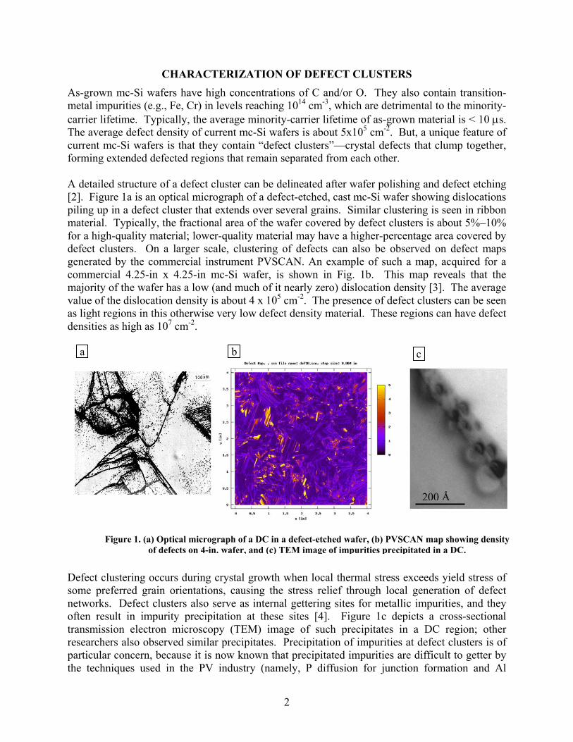
CHARACTERIZATION OF DEFECT CLUSTERS As-grown mc-Si wafers have high concentrations of C and/or O. They also contain transition-metal impurities (e.g., Fe, Cr) in levels reaching 1014 cm-3, which are detrimental to the minority-carrier lifetime. Typically, the average minority-carrier lifetime of as-grown material is < 10 µs. The average defect density of current mc-Si wafers is about 5x105 cm-2. But, a unique feature of current mc-Si wafers is that they contain “defect clusters”—crystal defects that clump together, forming extended defected regions that remain separated from each other. A detailed structure of a defect cluster can be delineated after wafer polishing and defect etching [2]. Figure 1a is an optical micrograph of a defect-etched, cast mc-Si wafer showing dislocations piling up in a defect cluster that extends over several grains. Similar clustering is seen in ribbon material. Typically, the fractional area of the wafer covered by defect clusters is about 5%–10% for a high-quality material; lower-quality material may have a higher-percentage area covered by defect clusters. On a larger scale, clustering of defects can also be observed on defect maps generated by the commercial instrument PVSCAN. An example of such a map, acquired for a commercial 4.25-in x 4.25-in mc-Si wafer, is shown in Fig. 1b. This map reveals that the majority of the wafer has a low (and much of it nearly zero) dislocation density [3]. The average value of the dislocation density is about 4 x 105 cm-2. The presence of defect clusters can be seen as light regions in this otherwise very low defect density material. These regions can have defect densities as high as 107 cm-2.
Defect clustering occurs during crystal growth when local thermal stress exceeds yield stress of some preferred grain orientations, causing the stress relief through local generation of defect networks. Defect clusters also serve as internal gettering sites for metallic impurities, and they often result in impurity precipitation at these sites [4]. Figure 1c depicts a cross-sectional transmission electron microscopy (TEM) image of such precipitates in a DC region; other researchers also observed similar precipitates. Precipitation of impurities at defect clusters is of particular concern, because it is now known that precipitated impurities are difficult to getter by the techniques used in the PV industry (namely, P diffusion for junction formation and Al
Figure 1. (a) Optical micrograph of a DC in a defect-etched wafer, (b) PVSCAN map showing density of defects on 4-in. wafer, and (c) TEM image of impurities precipitated in a DC.
a c
b
200 Å
3
alloying for back-contact formation). Hence, defect clusters have an important bearing on the development of new impurity-gettering methods that must dissolve the precipitates during gettering.
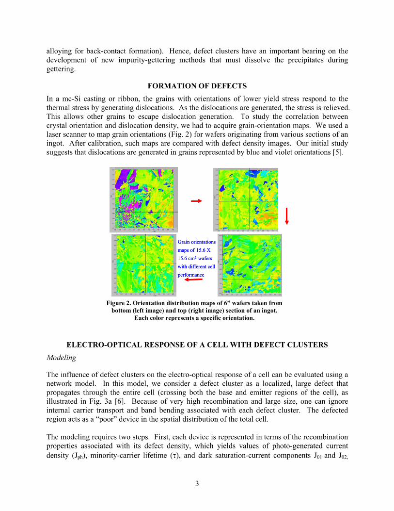
FORMATION OF DEFECTS In a mc-Si casting or ribbon, the grains with orientations of lower yield stress respond to the thermal stress by generating dislocations. As the dislocations are generated, the stress is relieved. This allows other grains to escape dislocation generation. To study the correlation between crystal orientation and dislocation density, we had to acquire grain-orientation maps. We used a laser scanner to map grain orientations (Fig. 2) for wafers originating from various sections of an ingot. After calibration, such maps are compared with defect density images. Our initial study suggests that dislocations are generated in grains represented by blue and violet orientations [5].
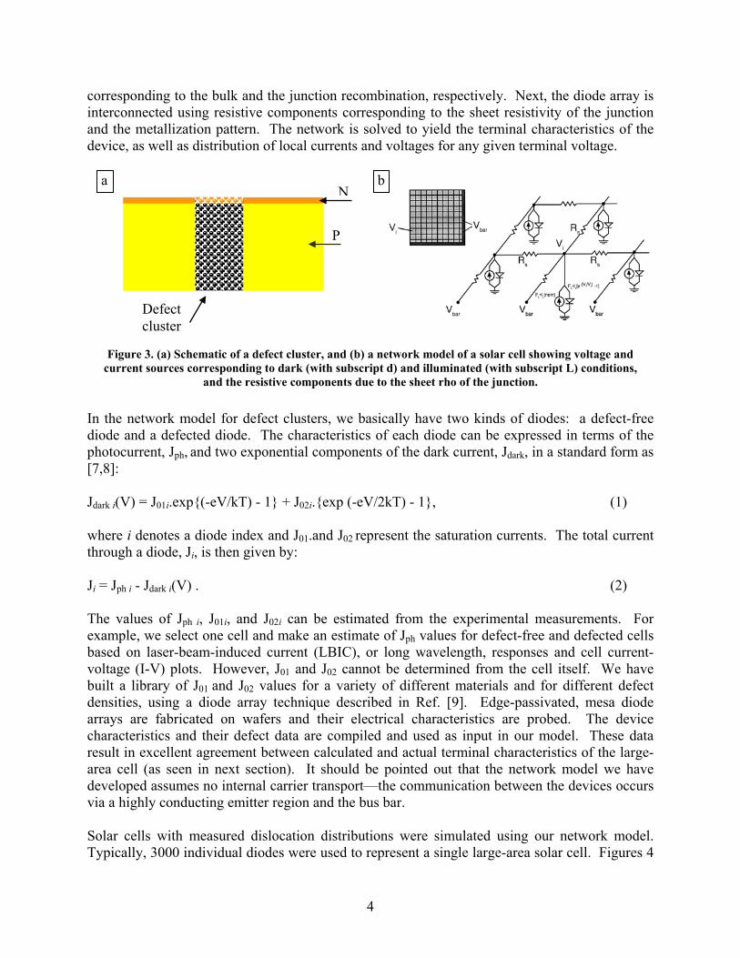
ELECTRO-OPTICAL RESPONSE OF A CELL WITH DEFECT CLUSTERS Modeling The influence of defect clusters on the electro-optical response of a cell can be evaluated using a network model. In this model, we consider a defect cluster as a localized, large defect that propagates through the entire cell (crossing both the base and emitter regions of the cell), as illustrated in Fig. 3a [6]. Because of very high recombination and large size, one can ignore internal carrier transport and band bending associated with each defect cluster. The defected region acts as a “poor” device in the spatial distribution of the total cell. The modeling requires two steps. First, each device is represented in terms of the recombination properties associated with its defect density, which yields values of photo-generated current density (Jph), minority-carrier lifetime (τ), and dark saturation-current components J01 and J02,
Grain orientations maps of 15.6 X 15.6 cm2 wafers with different cell performance
Grain orientations maps of 15.6 X 15.6 cm2 wafers with different cell performance
Figure 2. Orientation distribution maps of 6” wafers taken from
bottom (left image) and top (right image) section of an ingot. Each color represents a specific orientation.
4
corresponding to the bulk and the junction recombination, respectively. Next, the diode array is interconnected using resistive components corresponding to the sheet resistivity of the junction and the metallization pattern. The network is solved to yield the terminal characteristics of the device, as well as distribution of local currents and voltages for any given terminal voltage.
In the network model for defect clusters, we basically have two kinds of diodes: a defect-free diode and a defected diode. The characteristics of each diode can be expressed in terms of the photocurrent, Jph, and two exponential components of the dark current, Jdark, in a standard form as [7,8]: Jdark i(V) = J01i.exp{(-eV/kT) - 1} + J02i.{exp (-eV/2kT) - 1}, (1) where i denotes a diode index and J01.and J02 represent the saturation currents. The total current through a diode, Ji, is then given by: Ji = Jph i - Jdark i(V) . (2) The values of Jph i, J01i, and J02i can be estimated from the experimental measurements. For example, we select one cell and make an estimate of Jph values for defect-free and defected cells based on laser-beam-induced current (LBIC), or long wavelength, responses and cell current-voltage (I-V) plots. However, J01 and J02 cannot be determined from the cell itself. We have built a library of J01 and J02 values for a variety of different materials and for different defect densities, using a diode array technique described in Ref. [9]. Edge-passivated, mesa diode arrays are fabricated on wafers and their electrical characteristics are probed. The device characteristics and their defect data are compiled and used as input in our model. These data result in excellent agreement between calculated and actual terminal characteristics of the large-area cell (as seen in next section). It should be pointed out that the network model we have developed assumes no internal carrier transport—the communication between the devices occurs via a highly conducting emitter region and the bus bar. Solar cells with measured dislocation distributions were simulated using our network model. Typically, 3000 individual diodes were used to represent a single large-area solar cell. Figures 4
Figure 3. (a) Schematic of a defect cluster, and (b) a network model of a solar cell showing voltage and current sources corresponding to dark (with subscript d) and illuminated (with subscript L) conditions,
and the resistive components due to the sheet rho of the junction.
a N
P
Defect cluster
b
5
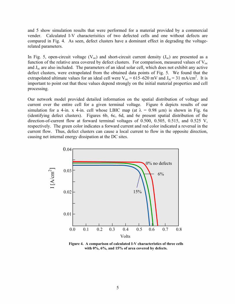
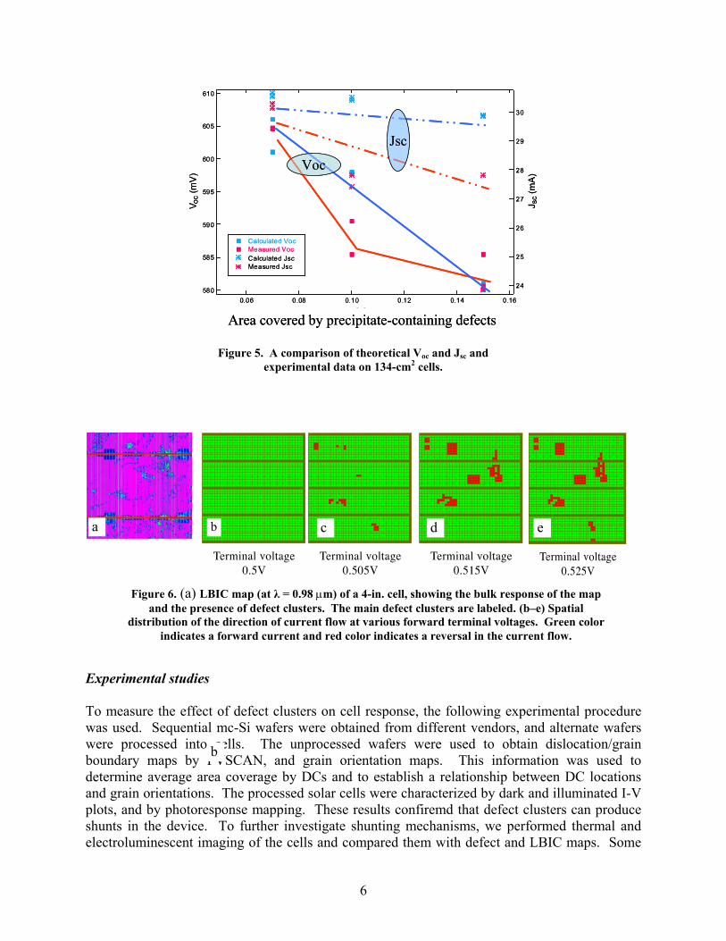
and 5 show simulation results that were performed for a material provided by a commercial vender. Calculated I-V characterisitics of two defected cells and one without defects are compared in Fig. 4. As seen, defect clusters have a dominant effect in degrading the voltage-related parameters. In Fig. 5, open-circuit voltage (Voc) and short-circuit current density (Jsc) are presented as a function of the relative area covered by defect clusters. For comparison, measured values of Voc and Jsc are also included. The parameters of an ideal solar cell, which does not exhibit any active defect clusters, were extrapolated from the obtained data points of Fig. 5. We found that the extrapolated ultimate values for an ideal cell were Voc = 615–620 mV and Jsc = 31 mA/cm2. It is important to point out that these values depend strongly on the initial material properties and cell processing. Our network model provided detailed information on the spatial distribution of voltage and current over the entire cell for a given terminal voltage. Figure 6 depicts results of our simulation for a 4-in. x 4-in. cell whose LBIC map (at λ = 0.98 µm) is shown in Fig. 6a (identifying defect clusters). Figures 6b, 6c, 6d, and 6e present spatial distribution of the direction-of-current flow at forward terminal voltages of 0.500, 0.505, 0.515, and 0.525 V, respectively. The green color indicates a forward current and red color indicated a reversal in the current flow. Thus, defect clusters can cause a local current to flow in the opposite direction, causing net internal energy dissipation at the DC sites.
0.04
0.03
0.02
0.01
0% no defects
15%
6%
0.0 0.1 0.2 0.3 0.4 0.5 0.6 0.7 0.8 Volts
I [A
/cm
2 ]
Figure 4. A comparison of calculated I-V characteristics of three cells with 0%, 6%, and 15% of area covered by defects.
6
Experimental studies To measure the effect of defect clusters on cell response, the following experimental procedure was used. Sequential mc-Si wafers were obtained from different vendors, and alternate wafers were processed into cells. The unprocessed wafers were used to obtain dislocation/grain boundary maps by PVSCAN, and grain orientation maps. This information was used to determine average area coverage by DCs and to establish a relationship between DC locations and grain orientations. The processed solar cells were characterized by dark and illuminated I-V plots, and by photoresponse mapping. These results confiremd that defect clusters can produce shunts in the device. To further investigate shunting mechanisms, we performed thermal and electroluminescent imaging of the cells and compared them with defect and LBIC maps. Some
Figure 5. A comparison of theoretical Voc and Jsc and experimental data on 134-cm2 cells.
Voc
Jsc
Area covered by precipitate-containing defects
Voc
Jsc
Area covered by precipitate-containing defects
Figure 6. (a) LBIC map (at λ = 0.98 µm) of a 4-in. cell, showing the bulk response of the map and the presence of defect clusters. The main defect clusters are labeled. (b–e) Spatial
distribution of the direction of current flow at various forward terminal voltages. Green color indicates a forward current and red color indicates a reversal in the current flow.
a c d e
b
b

7
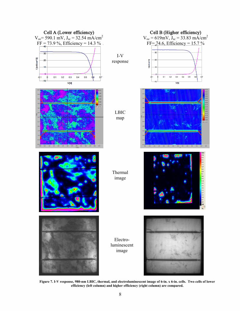
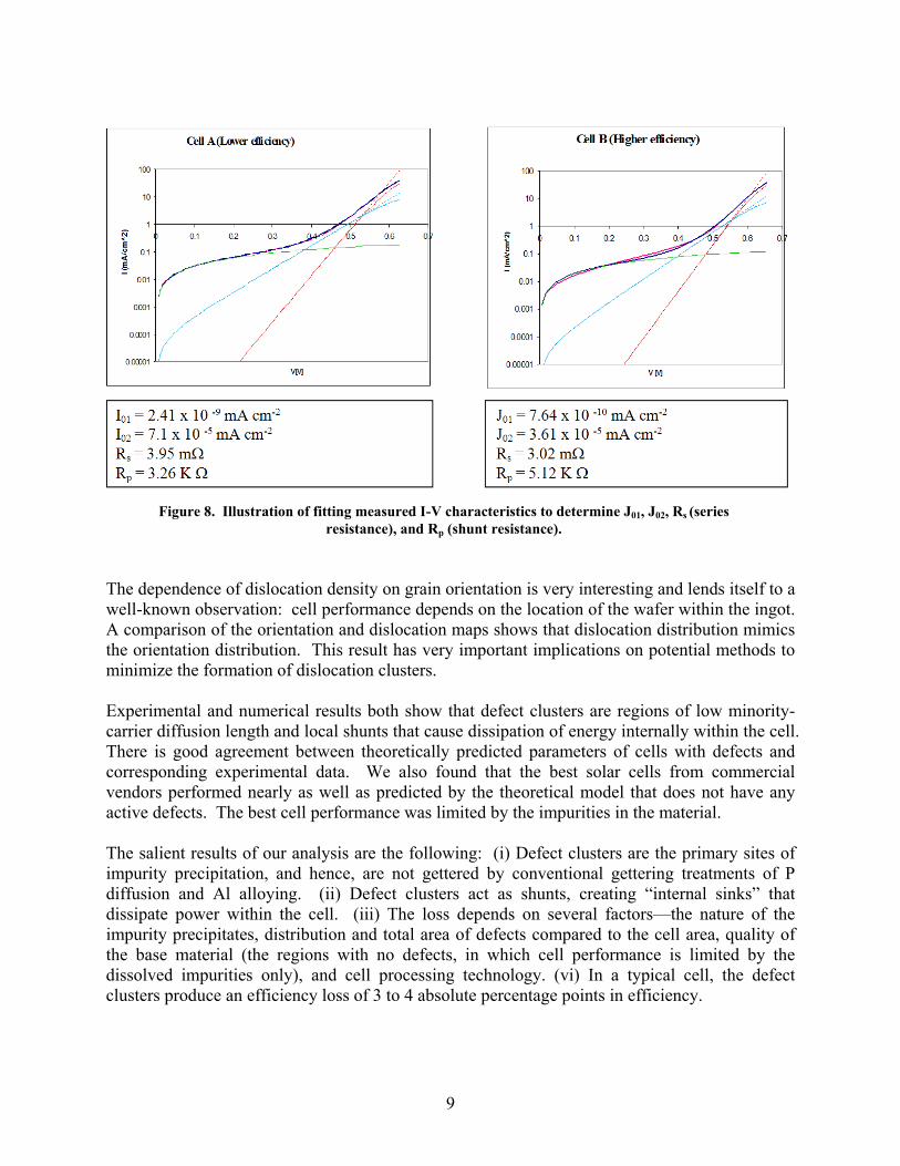
samples were used to perform cross-sectional analyses by TEM, atomic force microscopy (AFM), and capacitive atomic force microscopy (CFM). A comparison of two 6-in. cells labeled A and B is presented in Figs. 7 and 8. These two cells were chosen because they belong to two different efficiency categories. The efficiency of cells A and B are 14.3% and 15.7%, respectively. Figure 7 includes light and dark I-V response, basic cell parameters, LBIC maps for wavelength of 980 nm, as well as thermal and electroluminescent images. It can be observed that all three cell parameters—Voc, Jsc, and fill factor (FF)—are lower in the case of cell A. Further investigation of LBIC maps clearly revealed the structural difference between the cells. Cell B yielded a very uniform response over the entire area, with only a few spots with active defects. Contrary to cell B, cell A contains extensive active defect clusters that reveal themselves as regions of lower response. In general, thermal images show shunting areas where the energy radiates outward in the form of heat. For cell A, much heat is generated in various areas of the cell. The locations of these hot spots overlap with areas of low LBIC response. Therefore, it is clear that active defect clusters are responsible for poor performance of this cell. For higher-efficiency cell B, there are much fewer hot spots. Comparing the figures, it can also be observed that the hot spots and active defect clusters are not coincident. This means that some other mechanisms dominate in shunting generation in cell B. Electroluminescent maps in Fig. 7 clearly revealed the material’s nonuniformities. The location and size of active defect clusters can easily be determined. A very good correlation between LBIC and electroluminescent maps was found for cells with both good and bad performance. Another useful and complementary approach to investigate the influence of DCs is to examine the electronic characteristics of the entire cell by dissecting the dark and illuminated I-V plots. Here, we show some results of deriving important parameters that characterize the behavior of a cell by fitting the experimentally measured dark I-V plots with the theoretical two-diode model (i.e., applying Eq.[1] to the entire cell). It is important to recognize that we are obtaining lumped parameters of a distributed device. This procedure yields J01, J02, series resistance, and shunt resistance of each device. The quality of the fit can be determined by regenerating a theoretical I-V plot and comparing it with the experimental plot. Figures 8a and 8b show the values of the parameter values determined by this procedure for two cells described in Fig. 7. Figure 8 also shows that the theoretical and experimental I-V plots have excellent agreement. One can see that the higher-efficiency device, which contains a lower density of DCs, has lower values of J01 and J02, a lower series resistance, and higher shunt resistance.
CONCLUSIONS This paper presents a combination of numerical and experimental methods that were used to characterize defect clusters in mc-Si solar cells. In particular, we described a defect-generation mechanism, grain-orientation effect, interaction of defects with impurities, effect of defect distribution on cell performance, and shunting mechanisms associated with defect clusters.
8
Cell A (Lower efficiency) Voc= 590.1 mV, Jsc = 32.54 mA/cm2 FF = 73.9 %, Efficiency = 14.3 %
Cell B (Higher efficiency) Voc = 619mV, Jsc = 33.83 mA/cm2
FF= 74.6, Efficiency = 15.7 %
I-V response
LBIC map
Thermal image
Electro-luminescent
image
Figure 7. I-V response, 980-nm LBIC, thermal, and electroluminescent image of 6-in. x 6-in. cells. Two cells of lower efficiency (left column) and higher efficiency (right column) are compared.
9
The dependence of dislocation density on grain orientation is very interesting and lends itself to a well-known observation: cell performance depends on the location of the wafer within the ingot. A comparison of the orientation and dislocation maps shows that dislocation distribution mimics the orientation distribution. This result has very important implications on potential methods to minimize the formation of dislocation clusters. Experimental and numerical results both show that defect clusters are regions of low minority-carrier diffusion length and local shunts that cause dissipation of energy internally within the cell. There is good agreement between theoretically predicted parameters of cells with defects and corresponding experimental data. We also found that the best solar cells from commercial vendors performed nearly as well as predicted by the theoretical model that does not have any active defects. The best cell performance was limited by the impurities in the material. The salient results of our analysis are the following: (i) Defect clusters are the primary sites of impurity precipitation, and hence, are not gettered by conventional gettering treatments of P diffusion and Al alloying. (ii) Defect clusters act as shunts, creating “internal sinks” that dissipate power within the cell. (iii) The loss depends on several factors—the nature of the impurity precipitates, distribution and total area of defects compared to the cell area, quality of the base material (the regions with no defects, in which cell performance is limited by the dissolved impurities only), and cell processing technology. (vi) In a typical cell, the defect clusters produce an efficiency loss of 3 to 4 absolute percentage points in efficiency.
Figure 8. Illustration of fitting measured I-V characteristics to determine J01, J02, Rs (series resistance), and Rp (shunt resistance).
10
To recover the efficiency loss caused by cluster defects, it is necessary to either eliminate them during crystal growth or getter precipitated impurities at DC sites. The information gathered on defect clusters suggests potential techniques that can minimize defect cluster formation and/or dissolve precipitated impurities at temperatures and times that are compatible with solar cell fabrication; these techniques offer the potential to raise efficiency of mc-Si solar cells to >20%. An intuitive approach to mitigating the influence of defect clusters would be to dissolve the precipitates by a high-temperature treatment prior to or during gettering. A new approach, recently developed at the National Renewable Energy Laboratory, dissolves impurity precipitates by using vacancy injection to lower the temperature needed for precipitate dissolution. REFERENCES 1. B.L. Sopori, Proc. ICDS-19, Trans Tech Pub., edited by G. Davies and M.H. Nazare, 527
(1997). 2. B.L. Sopori, J. Electrochem. Soc. 131, 667 (1984). 3. PVSCAN uses optical scattering from a defect-etched wafer to statistically count defects. It
is also fitted with capabilities to make LBIC and reflectance measurements at 0.63 and 0.98 µm. It is available from GT Solar Technologies, Nashua, NH 03054. Also see B.L. Sopori, U.S. Patent 5,581,346.
4. T. Buonassisi, O.F. Vyvenko, A.A. Istratov, E.R. Weber, G. Hahn, D. Sontag, J.P. Rakotoniaina, O. Breitenstein, J. Isenberg, and R. Schindler, J. Appl. Phys. 95, 1556 (2004).
5. B. Sopori, P. Rupnowski, D. Balzar, P. Sheldon, “Dislocation Generation in Si: A Thermo-Mechanical Model Based on Measurable Parameters”, Conference Record of the 2006 IEEE 4th World Conference on Photovoltaic Energy Conversion, May 7-12, 2006, 936 - 939
6. B.L. Sopori and R.A. Murphy, Proceedings of 12th European Photovoltaic Solar Energy Conference, April 1994, Amsterdam, The Netherlands, 1797.
7. J.G. Fossum and F.A. Lindholm., IEEE Trans. ED-27 692(1980). 8. B.L. Sopori, R.A. Murphy, and C. Marshall, Proceedings of the 23rd IEEE Photovoltaic
Specialists Conference, Louisville, Kentucky, May 10–14, 1993, 190. 9. B.L. Sopori, Appl. Phys. Lett. 52, 1718 (1988).

F1147-E(10/2008)
REPORT DOCUMENTATION PAGE Form Approved OMB No. 0704-0188
The public reporting burden for this collection of information is estimated to average 1 hour per response, including the time for reviewing instructions, searching existing data sources, gathering and maintaining the data needed, and completing and reviewing the collection of information. Send comments regarding this burden estimate or any other aspect of this collection of information, including suggestions for reducing the burden, to Department of Defense, Executive Services and Communications Directorate (0704-0188). Respondents should be aware that notwithstanding any other provision of law, no person shall be subject to any penalty for failing to comply with a collection of information if it does not display a currently valid OMB control number. PLEASE DO NOT RETURN YOUR FORM TO THE ABOVE ORGANIZATION. 1. REPORT DATE (DD-MM-YYYY)
February 2009 2. REPORT TYPE
Conference Paper 3. DATES COVERED (From - To)
17-19 March 2009 4. TITLE AND SUBTITLE
Performance Limitations of mc-Si Solar Cells Caused by Defect Clusters: Preprint
5a. CONTRACT NUMBER DE-AC36-08-GO28308
5b. GRANT NUMBER
5c. PROGRAM ELEMENT NUMBER
6. AUTHOR(S) B. Sopori. P. Rupnowski, V. Mehta, V. Budhraja, S. Johnston, N. Call, H. Moutinho, M. Al-Jassim, A. Shaikh, M. Seacrist, and D. Carlson
5d. PROJECT NUMBER NREL/CP-520-45012
5e. TASK NUMBER PVA93110
5f. WORK UNIT NUMBER
7. PERFORMING ORGANIZATION NAME(S) AND ADDRESS(ES) National Renewable Energy Laboratory 1617 Cole Blvd. Golden, CO 80401-3393
8. PERFORMING ORGANIZATION REPORT NUMBER NREL/CP-520-45012
9. SPONSORING/MONITORING AGENCY NAME(S) AND ADDRESS(ES)
10. SPONSOR/MONITOR'S ACRONYM(S) NREL
11. SPONSORING/MONITORING AGENCY REPORT NUMBER
12. DISTRIBUTION AVAILABILITY STATEMENT National Technical Information Service U.S. Department of Commerce 5285 Port Royal Road Springfield, VA 22161
13. SUPPLEMENTARY NOTES
14. ABSTRACT (Maximum 200 Words) Multicrystalline silicon wafers used for solar cells exhibit defect clusters—localized crystal defects in and near grains of some specific orientations. Defect clusters are also dominant sites for impurity precipitation, and they remain ungettered and unpassivated through the solar cell processing. This paper describes characteristics of defect clusters, and shows, through theory and experiment, that defect clusters typically lower cell efficiency by 3 to 4 absolute percentage points. To recover this efficiency loss, it is necessary to getter precipitated impurities.
15. SUBJECT TERMS PV; multicrystalline silicon; solar cells; defect clusters; photogenerated current density; minority-carrier lifetime; dark saturation current; grain orientation;
16. SECURITY CLASSIFICATION OF: 17. LIMITATION OF ABSTRACT
UL
18. NUMBER OF PAGES
19a. NAME OF RESPONSIBLE PERSON a. REPORT
Unclassified b. ABSTRACT Unclassified
c. THIS PAGE Unclassified 19b. TELEPHONE NUMBER (Include area code)
Standard Form 298 (Rev. 8/98) Prescribed by ANSI Std. Z39.18