Embed Size (px)
Citation preview

123
Energy Systems in Electrical Engineering
Sherif HekalAhmed AllamAdel B. Abdel-RahmanRamesh K. Pokharel
Compact Size Wireless Power Transfer Using Defected Ground Structures

Energy Systems in Electrical Engineering
Series Editor
Muhammad H. Rashid, Florida Polytechnic University, Lakeland, USA

More information about this series at http://www.springer.com/series/13509

Sherif Hekal • Ahmed Allam •
Adel B. Abdel-Rahman •
Ramesh K. Pokharel
Compact Size WirelessPower Transfer UsingDefected Ground Structures
123

Sherif HekalFaculty of Engineering at ShoubraBenha UniversityCairo, Egypt
Ahmed AllamSchool of Electronics, Communications,and Computer EngineeringEgypt-Japan University of Scienceand TechnologyAlexandria, EgyptAdel B. Abdel-Rahman
Egypt-Japan University of Scienceand TechnologyAlexandria, Egypt
Ramesh K. PokharelKyushu UniversityFukuoka, Japan
ISSN 2199-8582 ISSN 2199-8590 (electronic)Energy Systems in Electrical EngineeringISBN 978-981-13-8046-4 ISBN 978-981-13-8047-1 (eBook)https://doi.org/10.1007/978-981-13-8047-1
© Springer Nature Singapore Pte Ltd. 2019This work is subject to copyright. All rights are reserved by the Publisher, whether the whole or partof the material is concerned, specifically the rights of translation, reprinting, reuse of illustrations,recitation, broadcasting, reproduction on microfilms or in any other physical way, and transmissionor information storage and retrieval, electronic adaptation, computer software, or by similar or dissimilarmethodology now known or hereafter developed.The use of general descriptive names, registered names, trademarks, service marks, etc. in thispublication does not imply, even in the absence of a specific statement, that such names are exempt fromthe relevant protective laws and regulations and therefore free for general use.The publisher, the authors and the editors are safe to assume that the advice and information in thisbook are believed to be true and accurate at the date of publication. Neither the publisher nor theauthors or the editors give a warranty, expressed or implied, with respect to the material containedherein or for any errors or omissions that may have been made. The publisher remains neutral with regardto jurisdictional claims in published maps and institutional affiliations.
This Springer imprint is published by the registered company Springer Nature Singapore Pte Ltd.The registered company address is: 152 Beach Road, #21-01/04 Gateway East, Singapore 189721,Singapore

To our families

Preface
The technology of wireless power transfer (WPT) has attracted considerableattention recently due to the increasing demand of wireless applications such asportable electronic devices, biomedical implants, and wireless buried sensors. WPTtechnology can be found also in contactless radio-frequency identification (RFID)and remote charging of electrical vehicles. It is beneficial to power electricaldevices in cases where interconnecting wires are inconvenient, dangerous, orimpossible. Wireless power transmission can be implemented by different methodsthat employ time-varying electric/magnetic (near-field) or electromagnetic(far-field) fields. Near-field (no-radiative) WPT systems have recently becomepopular as they are considered to be safe for health and provide high efficiency forshort and mid-range applications.
This book addresses the design challenges in the near-field WPT systems such ashigh efficiency, compact size, and long transmission range. Most of the near-fieldWPT systems depend upon magnetic resonant coupling (MRC) using 3D wireloops or helical antennas which are often bulky. This, in turn, poses technicaldifficulties for their use in small electronic devices and biomedical implants.Recently to get compact structures, the printed spiral coils (PSCs) have emerged asa candidate for low-profile WPT system. However, most of the MRC-WPT systemsthat use PSCs have limitations in the maximum achievable efficiency due to thefeeding method. Inductive feeding constrains the geometric dimensions of the maintransmitting (TX)/receiving (RX) resonators.
The book presents new low-profile designs for the TX/RX structures usingdifferent shapes of defected ground structures (DGSs), such as H, semi-H, andspiral-strip DGS. The main advantage of the DGS WPT system is the feedingtopology, where the power is transferred from/to the main TX/RX resonators byelectrical coupling. We gain two advantages from this feeding topology: Firstly, theexternal quality factor can be easily optimized by an additional capacitor connected
vii

between the feed/load microstrip line and the DGS resonator. Secondly, no limi-tations exist on the optimization of the DGS resonator parameters to achievemaximum power transfer efficiency, unlike the case of conventional inductivefeeding.
Chapter 1 presents an overview of the technology of wireless power transfer(WPT) which can be utilized in many applications such as charging mobile devicesand implanted biomedical devices as well as applications where interconnectingwires are inconvenient, dangerous, or impossible to implement, as in the cases ofwireless buried sensors and sterilized rooms. Different implementation methods arediscussed in brief by mentioning the current products that use these methods. Thebenefits of WPT are given by introducing the applications in our daily life and howthey make our life hassle-free. This chapter also presents the challenges WPTsystems face such as transfer efficiency, compact size, and transmission distance.After that, this chapter provides motivations to these vital topics that have attractedthe attention of many researchers recently.
Chapter 2 begins by discussing briefly the history of WPT over the last decades.The different techniques of transferring power wirelessly will be presented. Somecommercial products and applications that use WPT are shown. A review of thecurrent state of short-range WPT technology is given, and the trending researchtopics are noted. This chapter ends with a detailed explanation of the defectedground structures (DGSs) and their usage in microwave applications.
Chapter 3 describes the principle of operation of using the defected groundstructures (DGSs) as building blocks for WPT from circuit theory and microwavetheories point of views. All design parameters and equivalent circuit elements that areassociated with the proposed WPT systems will be defined. A more accurate circuitmodel is introduced to provide a better understanding of how the losses affect theefficiency of the WPT systems. This chapter also provides a detailed analysis of thedesign parameters that can realize the maximum achievable WPT efficiency. Anasymmetric size WPT system with high efficiency is developed by the implemen-tation of very compact size RX that can be embedded in the electronic consumingdevices or biomedical implants to be charged wirelessly by larger-size TX.
Chapter 4 reviews the different design methods that are currently being used inWPT systems. This chapter shows how the traditional design methods, whichdepend on iterative optimization, are not suitable due to a large amount of timeneeded to complete the design. This chapter provides an overview of the designmethods that depend on circuit analysis using the impedance (Z-) parameters or theadmittance (J-) inverters and discusses their principle of operation. A new designmethod is developed to represent the proposed WPT systems as a second-orderButterworth BPF using admittance inverters. A detailed mathematical analysis isperformed to investigate the new design method and its effectiveness to reach theoptimum design parameters and circuit elements accurately and fast. The noveldesign method is applicable to symmetric and asymmetric WPT systems. A design
viii Preface

case is given detailing the design procedure and the experimental results to verifythe new design method.
Chapter 5 reviews the outcomes of the work presented in the book and concludesthe book. Recommendations for future directions are also presented.
Shoubra, Egypt Sherif HekalAlexandria, Egypt Ahmed AllamQena, Alexandria, Egypt Adel B. Abdel-RahmanFukuoka, Japan Ramesh K. Pokharel
Preface ix

Acknowledgements
Contributions from many colleagues in Kyushu University, Japan, and Egypt-JapanUniversity of Science and Technology (E-JUST), Egypt, led to the completion ofthis book. Particularly, the authors would like to thank Professor Haruichi Kanaya,Associate Professor Hongting Jia, and Dr. Adel. Barakat. The authors would like tothank Professor Kuniaki Yoshitomi, Kyushu University, for his valuable coopera-tion and support in the designs fabrications and measurements.
The authors would like to acknowledge that this work was supported in part by aGrant-in-Aid for Scientific Research (C) under Grant 16K06301, in part by theVLSI Design and Education Center (VDEC) at the University of Tokyo in col-laboration with the Keysights Corporation, in part by the Egyptian Ministry ofHigher Education and Scientific Research (MoHESR), Cairo, Egypt, and in part byEgypt-Japan University of Science and Technology (E-JUST), Alexandria, Egypt.
xi

Contents
1 Introduction . . . . . . . . . . . . . . . . . . . . . . . . . . . . . . . . . . . . . . . . . . . 11.1 Overview of Wireless Power Transfer . . . . . . . . . . . . . . . . . . . . . 11.2 Applications of WPT . . . . . . . . . . . . . . . . . . . . . . . . . . . . . . . . . 31.3 Motivations of WPT . . . . . . . . . . . . . . . . . . . . . . . . . . . . . . . . . . 41.4 Challenges of WPT Systems Implementation . . . . . . . . . . . . . . . . 5
1.4.1 Non-radiative Systems . . . . . . . . . . . . . . . . . . . . . . . . . . . 51.4.2 Radiative Systems . . . . . . . . . . . . . . . . . . . . . . . . . . . . . . 6
References . . . . . . . . . . . . . . . . . . . . . . . . . . . . . . . . . . . . . . . . . . . . . 7
2 Basics of Wireless Power Transfer . . . . . . . . . . . . . . . . . . . . . . . . . . 92.1 Introduction . . . . . . . . . . . . . . . . . . . . . . . . . . . . . . . . . . . . . . . . 92.2 History of Wireless Power Transfer . . . . . . . . . . . . . . . . . . . . . . . 92.3 Wireless Power Transfer Methods . . . . . . . . . . . . . . . . . . . . . . . . 12
2.3.1 Capacitive Coupling . . . . . . . . . . . . . . . . . . . . . . . . . . . . 132.3.2 Inductive Coupling . . . . . . . . . . . . . . . . . . . . . . . . . . . . . 142.3.3 Resonant Inductive Coupling . . . . . . . . . . . . . . . . . . . . . . 152.3.4 Strong Resonant Inductive Coupling . . . . . . . . . . . . . . . . . 152.3.5 Electromagnetic (EM) Radiation . . . . . . . . . . . . . . . . . . . . 16
2.4 Implementation of Near-Field WPT Systems . . . . . . . . . . . . . . . . 172.5 Implementation of Far-Field WPT Systems . . . . . . . . . . . . . . . . . 192.6 Frequency Selection . . . . . . . . . . . . . . . . . . . . . . . . . . . . . . . . . . 232.7 Overview of Commercial Products Supporting WPT . . . . . . . . . . 24References . . . . . . . . . . . . . . . . . . . . . . . . . . . . . . . . . . . . . . . . . . . . . 26
3 Wireless Power Transfer Using DGSs . . . . . . . . . . . . . . . . . . . . . . . . 333.1 Introduction . . . . . . . . . . . . . . . . . . . . . . . . . . . . . . . . . . . . . . . . 333.2 An Overview on Defected Ground Structures (DGS) . . . . . . . . . . 353.3 WPT Systems Using DGSs . . . . . . . . . . . . . . . . . . . . . . . . . . . . . 38
xiii

3.3.1 H-Shape DGS . . . . . . . . . . . . . . . . . . . . . . . . . . . . . . . . . 383.3.2 Semi H-Shape . . . . . . . . . . . . . . . . . . . . . . . . . . . . . . . . . 453.3.3 Spiral-Strips DGS . . . . . . . . . . . . . . . . . . . . . . . . . . . . . . 53
3.4 Design Method of the DGS-WPT Systems . . . . . . . . . . . . . . . . . . 583.5 Fabrication and Measurements . . . . . . . . . . . . . . . . . . . . . . . . . . . 643.6 Power Transmission Through the Human Body . . . . . . . . . . . . . . 683.7 Power Handling Capability of the Proposed WPT Systems . . . . . . 70References . . . . . . . . . . . . . . . . . . . . . . . . . . . . . . . . . . . . . . . . . . . . . 70
4 Design Methods . . . . . . . . . . . . . . . . . . . . . . . . . . . . . . . . . . . . . . . . 734.1 Introduction . . . . . . . . . . . . . . . . . . . . . . . . . . . . . . . . . . . . . . . . 734.2 Design Method #1 . . . . . . . . . . . . . . . . . . . . . . . . . . . . . . . . . . . 734.3 Design Method #2 . . . . . . . . . . . . . . . . . . . . . . . . . . . . . . . . . . . 784.4 Verification of Design Method #2 . . . . . . . . . . . . . . . . . . . . . . . . 80
4.4.1 Symmetric WPT System . . . . . . . . . . . . . . . . . . . . . . . . . 804.4.2 Asymmetric WPT System . . . . . . . . . . . . . . . . . . . . . . . . 83
References . . . . . . . . . . . . . . . . . . . . . . . . . . . . . . . . . . . . . . . . . . . . . 85
5 Future Directions . . . . . . . . . . . . . . . . . . . . . . . . . . . . . . . . . . . . . . . 875.1 Summary . . . . . . . . . . . . . . . . . . . . . . . . . . . . . . . . . . . . . . . . . . 875.2 Future Directions . . . . . . . . . . . . . . . . . . . . . . . . . . . . . . . . . . . . 88References . . . . . . . . . . . . . . . . . . . . . . . . . . . . . . . . . . . . . . . . . . . . . 91
xiv Contents

About the Authors
Sherif Hekal is currently an Assistant Professor at the Department of Electronicsand Communications Engineering, Faculty of Engineering at Shoubra—BenhaUniversity, Cairo. He received his B.Sc. and M.Sc. degrees in ElectricalEngineering from the same university in 2007 and 2012, respectively. He receivedhis Ph.D. from the Egypt-Japan University of Science and Technology (E-JUST) inElectronics and Communications Engineering in 2016. As part of his Ph.D. pro-gram, he spent time at the Faculty of Information Science and ElectricalEngineering, Kyushu University, Fukuoka, Japan. Dr. Hekal also worked as acommunications engineer at Motorola Co. Ltd. and Nokia Siemens Networks in thefield of 2G/3G RF optimization. His research interests include RF/microwaveapplications, antennas, wireless power transfer, and energy harvesting systems.
Dr. Ahmed Allam is currently an Associate Professor at the Department ofElectronics and Communications Engineering, Egypt-Japan University of Scienceand Technology, Alexandria, Egypt. He received his B.Sc. in Electrical Engineeringfrom Alexandria University, Egypt, and his M.Eng. and Ph.D. from the Universityof Alberta, Canada. From April 1994 to January 1998, he worked as an instrumentengineer with Schlumberger. From May 2000 to September 2001, he was withMurandi Communications Ltd., Calgary, Alberta, where he worked on RF trans-ceivers design. From April 2007 to April 2008, he worked on RF CMOS trans-ceivers design at Scanimetrics Inc., Edmonton, Alberta. His research interestsinclude the design of RF circuits and systems.
Adel B. Abdel-Rahman is currently a Professor at the Department of Electronicsand Communications Engineering, Egypt-Japan University of Science andTechnology, Alexandria, Egypt. He received his B.S. and M.S. in ElectricalEngineering, Communication, and Electronics from Assiut University, Egypt, andhis Dr.-Ing. degree in Communication Engineering from Otto von GuerickeUniversity, Germany in 2005. Since October 2006, he has been an AssistantProfessor at the Electrical Engineering Department, South Valley University, Qena,Egypt. He has published more than 120 refereed journal and conference papers and
xv

has two patents. He was the Executive Director for Information andCommunication Technology, South Valley University, from 2010–2012. SinceOctober 2012, he joined the School of Electronics, Communications and ComputerEngineering, Egypt-Japan University of Science and Technology (E-JUST),Alexandria, Egypt, and has been the Dean of the Faculty of Computers andInformation, South Valley University from 2016–2018. His research interestsinclude the design and analysis of antennas, filters, millimeter-wave devices, WPT,and metamaterials and their application in wireless communication, as well asoptimization techniques with applications to microwave devices and antenna arrays.
Ramesh K. Pokharel is a Professor in the Department of I&E Visionaries atKyushu University. He received M.E. and PhD in Electrical Engineering from theUniversity of Tokyo, Japan in 2000 and 2003, respectively. In April 2005, he joinedthe Graduate School of Information Science and Electrical Engineering, KyushuUniversity. He was the secretary of IEEE MTT-S Japan Society from Jan. 2012 toDec. 2013 and the deputy-chair of the Education committee of IEEE-MTT-S JapanSociety from Jan. 2014 to Dec. 2017 and has been serving as the chair of the samecommittee since 2017. His current research interests include low cost RFIC andanalog circuits for microwave and millimeter wave wireless communications, andon-chip meta-materials in CMOS.
xvi About the Authors

Abbreviations
2-D Two Dimensional3-D Three DimensionalA4WP Alliance for Wireless PowerAC Alternating CurrentADS Advanced Design SystemsBPF Band Pass FilterBSF Band Stop FilterCST Computer Simulation TechnologyDC Direct CurrentDCP Dual Circularly PolarizedDGS Defected Ground StructureEIRP Effective Isotropic Radiated PowerEM ElectromagneticFCC Federal Communications CommitteeHFSS High Frequency Structures SimulatorIMN Impedance Matching NetworkIPT Inductive Power TransferISM Industrial Scientific MedicalJAXA Japanese Space AgencyLHCP Left hand circular polarizationLOS line-of-sightMCR Magnetically Coupled ResonanceMPE Maximum Permissible ExposureMRC Magnetic Resonant CouplingNASA National Aeronautics and Space AdministrationPCB Printed Circuit BoardPCE Power conversion efficiencyPMA Power Matters AlliancePSC Printed Spiral CoilPV Photovoltaic
xvii

RAMP Raytheon Airborne Microwave PlatformRectenna Rectifying AntennaRF Radio FrequencyRFID Radio Frequency IdentificationRHCP right hand circular polarizationRX Receiver / ReceivingSAE Society of Automotive EngineersSAR Specific Absorption RateSHARP Stationary High-Altitude Relay PlatformSMD surface mountedSPS Solar Power SatelliteTX Transmitter / TransmittingUAV Unmanned Aerial VehiclesWBAN wireless body area networkWPC Wireless Power ConsortiumWPT Wireless Power TransferWRSN wireless renewable sensor network
xviii Abbreviations

Nomenclature
Symbols
L Self-inductanceM Mutual inductancek Coupling coefficientCP Parallel capacitanceCS Series capacitanceh Transmission distanceD Outer diameter of resonatord Inner diameter of resonatoru Fill factorN Number of turns of printed spiral
Units
µ0 Permeability of free space (4p 10−7 Henry/m)e0 Permittivity of free space (8.85 10−12 Farad/m)
xix
List of Figures
Fig. 1.1 Implementation of WPT systems using a near-field coupling,and b far-field radiations. . . . . . . . . . . . . . . . . . . . . . . . . . . . . . . 2
Fig. 1.2 Some of the most famous WPT applications [9]. . . . . . . . . . . . . 3Fig. 1.3 Motivations of using wireless power transfer systems. . . . . . . . . 4Fig. 1.4 Dream of wireless power society [10]. . . . . . . . . . . . . . . . . . . . . 5Fig. 2.1 Tesla WPT experiments a Theory of operation. b Tesla’s
lab and tower [7] . . . . . . . . . . . . . . . . . . . . . . . . . . . . . . . . . . . . 10Fig. 2.2 First-ever laser-powered aircraft, designed and built
by a team of NASA researchers [13] . . . . . . . . . . . . . . . . . . . . . 11Fig. 2.3 WPT systems using capacitive coupling . . . . . . . . . . . . . . . . . . . 13Fig. 2.4 WPT using inductive coupling . . . . . . . . . . . . . . . . . . . . . . . . . . 14Fig. 2.5 WPT using resonant inductive coupling . . . . . . . . . . . . . . . . . . . 15Fig. 2.6 WPT using strong resonant inductive coupling . . . . . . . . . . . . . . 16Fig. 2.7 Schematic of the experimental setup of strongly coupled
magnetic resonances implemented by the MIT team [26] . . . . . . 18Fig. 2.8 Far-field wireless charging [30]. . . . . . . . . . . . . . . . . . . . . . . . . . 20Fig. 2.9 ISM band . . . . . . . . . . . . . . . . . . . . . . . . . . . . . . . . . . . . . . . . . . 23Fig. 2.10 Powercast wireless charging system a Transmitter.
b Receiver. c Wireless rechargeable sensor system. . . . . . . . . . . 25Fig. 3.1 Different shapes of DGSs. a Circular head dumbbell.
b Triangular head dumbbell. c Square head dumbbell. d SpiralDGS. e Meander lines. f U-slot. g Square open-loop with a slotin middle section . . . . . . . . . . . . . . . . . . . . . . . . . . . . . . . . . . . . 35
Fig. 3.2 Equivalent RLC circuit of DGS unit . . . . . . . . . . . . . . . . . . . . . . 36Fig. 3.3 Conventional design and analysis method of DGS . . . . . . . . . . . 37Fig. 3.4 Quasi-static modeling [38]. a Unit cell DGS. b Surface
current on the ground plane . . . . . . . . . . . . . . . . . . . . . . . . . . . . 37
xxi

Fig. 3.5 Schematic equivalent current sheet (filament model) [38] . . . . . . 38Fig. 3.6 Hekal et al. [1] a Proposed coupled H-shape DGS resonators
WPT system. b H-shape DGS resonator as BSF at 300 MHz.c Simulated current distribution at phases (90°, and 270°) . . . . . 39
Fig. 3.7 Verification of the quasi-static model for H-shape DGS.a Equivalent circuit [1]. b Comparison between |S-parameters|of EM and circuit simulations [1] . . . . . . . . . . . . . . . . . . . . . . . . 40
Fig. 3.8 PCB layout of H-shape DGS resonator for the proposedWPT system [1] . . . . . . . . . . . . . . . . . . . . . . . . . . . . . . . . . . . . . 41
Fig. 3.9 An equivalent circuit of the proposed WPT system usingcoupled H-shape DGS resonators [1] . . . . . . . . . . . . . . . . . . . . . 42
Fig. 3.10 Measurement setup of the fabricated WPT systems usingH-shape DGS resonators [1] . . . . . . . . . . . . . . . . . . . . . . . . . . . . 44
Fig. 3.11 Comparison between the measured and the simulated|S-parameters| of the proposed WPT system using H-shapeDGS resonators at 300 MHz and at transmission distanceh = 13 mm [1] . . . . . . . . . . . . . . . . . . . . . . . . . . . . . . . . . . . . . . 44
Fig. 3.12 3D schematic view of the proposed WPT system with therepresentation of the stub as a lumped capacitor [1] . . . . . . . . . . 45
Fig. 3.13 Representation of the stub as a lumped capacitor. a CSTSimulated |S-parameters| [1]. b ADS Simulated|S-parameters| [1] . . . . . . . . . . . . . . . . . . . . . . . . . . . . . . . . . . . . 46
Fig. 3.14 Misalignment studies for H-shape DGS-WPT system(20 20 mm2). a Schematic of misalignment due tohorizontal shift and orientation [1]. b EM simulated WPTefficiency versus misalignment shifts [1]. c EM simulatedWPT efficiency versus orientation angle [1] . . . . . . . . . . . . . . . . 47
Fig. 3.15 Schematic of semi H-shape DGS resonator [1] . . . . . . . . . . . . . . 48Fig. 3.16 The proposed WPT system based on semi H-shape DGS
resonators [1]. a PCB layout of a single resonator. b 3Dschematic view. c equivalent circuit . . . . . . . . . . . . . . . . . . . . . . 48
Fig. 3.17 EM simulated magnetic field distribution of the coupled semiH-shape resonators WPT system at 300 MHz at plane X = 0[1]. a U = 0°. b U = 90°. c U = 180°. d U = 270° . . . . . . . . . . 50
Fig. 3.18 Measurement setup of the fabricated WPT systems using semiH-shape DGS resonators [1] . . . . . . . . . . . . . . . . . . . . . . . . . . . . 50
Fig. 3.19 Comparison between the measured and the simulated|S-parameters| of the proposed WPT system using semiH-shape DGS resonators at 300 MHz and at a transmissiondistance h = 25 mm [1] . . . . . . . . . . . . . . . . . . . . . . . . . . . . . . . 51
Fig. 3.20 Measured WPT efficiency versus transmission distance (h) forH-shape and semi H-shape DGS resonators at 300 MHz [1] . . . 51
Fig. 3.21 Comparison between the measured power transfer efficiencyversus misalignment [1] due a horizontal shift, and b different
xxii List of Figures

orientation angles for H-shape (20 20 mm2) and semiH-shape (21 21 mm2) DGS-WPT systems . . . . . . . . . . . . . . . 52
Fig. 3.22 Comparison between three different shapes of DGS (H-shape,semi H-shape, spiral-strips DGS) [2]. a Current distribution.b Computed self-inductance . . . . . . . . . . . . . . . . . . . . . . . . . . . . 54
Fig. 3.23 Proposed spiral-strips DGS resonator as BSF [2]. a PCBlayout. b, c EM and circuit simulated |S-parameters| embeddedwith equivalent circuit extracted by quasi-static modeling andanalogy with one-pole Butterworth BSF response,respectively . . . . . . . . . . . . . . . . . . . . . . . . . . . . . . . . . . . . . . . . . 55
Fig. 3.24 a Model of the proposed spiral-strips DGS-WPT system,and b its EM simulated |S11| & |S21| . . . . . . . . . . . . . . . . . . . . . . 57
Fig. 3.25 a PCB layout of the realized TX/RX structure [2].b The equivalent circuit of the proposed WPT system.c Analysis of the equivalent circuit using J-inverters [48]. . . . . . 58
Fig. 3.26 The proposed applications for wireless charging of mobilehandsets [3] . . . . . . . . . . . . . . . . . . . . . . . . . . . . . . . . . . . . . . . . 59
Fig. 3.27 Investigation of the computed U-factor of the coupledresonators versus the width Wt,i and separation si for theproposed symmetric WPT systems (50 50 mm2) [3] . . . . . . . 60
Fig. 3.28 Optimum WPT efficiency at different transmission distancesfor the symmetric WPT system (50 50 mm2) . . . . . . . . . . . . . 61
Fig. 3.29 Optimum WPT efficiency at different transmission distancesfor the asymmetric WPT system . . . . . . . . . . . . . . . . . . . . . . . . . 62
Fig. 3.30 Magnetic field distribution of the symmetric (50 50 mm2)WPT system at phases Ф = 0°, 45°, 90°, 135°,and 180° [3] . . . . . . . . . . . . . . . . . . . . . . . . . . . . . . . . . . . . . . . . 63
Fig. 3.31 Magnetic field distribution of the asymmetric WPT system(TX 50 50 mm2 & RX 30 30 mm2) at phases Ф = 0°,45°, 90°, 135°, and 180° [3] . . . . . . . . . . . . . . . . . . . . . . . . . . . . 64
Fig. 3.32 Measurement setup of the fabricated WPT systems (Symmetric50 50 mm2, Symmetric 30 30 mm2, and AsymmetricTX = 50 50 mm2, RX = 30 30 mm2) [3] . . . . . . . . . . . . . . 65
Fig. 3.33 Comparison between the measured and the simulated|S-parameters|. a Symmetric 50 50 mm2 at h = 50 mm.b Symmetric 30 30 mm2 at h = 30 mm. c AsymmetricTX = 50 50 mm2, RX = 30 30 mm2 at h = 40 mm.d Measured WPT efficiency versus different transmissiondistances [3] . . . . . . . . . . . . . . . . . . . . . . . . . . . . . . . . . . . . . . . . 65
Fig. 3.34 Fabricated designs and measurements of the proposedspiral-strips DGS-WPT system at f0 = 13.5 MHz [3] . . . . . . . . . 67
Fig. 3.35 Simulated and measured |S-parameters| for the proposedspiral-strips DGS-WPT system at h = 10 cm and f0 = 13.5MHz [3] . . . . . . . . . . . . . . . . . . . . . . . . . . . . . . . . . . . . . . . . . . . 68
List of Figures xxiii

Fig. 3.36 Representing human life tissue effects on the efficiency ofpower transmission by insertion of a human hand . . . . . . . . . . . 69
Fig. 3.37 Comparison between the measured |S-parameters| of the WPTsystem in Fig. 3.36 with and without a human hand presence,where the transmission distance is 50 mm . . . . . . . . . . . . . . . . . 69
Fig. 4.1 A wireless power transfer systems using two coils [3] . . . . . . . . 74Fig. 4.2 Equivalent circuits of admittance inverters in Fig. 4.1b [3]. . . . . 75Fig. 4.3 Flowchart of design method #1. . . . . . . . . . . . . . . . . . . . . . . . . . 77Fig. 4.4 a Proposed system block diagram. b Its equivalent circuit.
c Equivalent circuit based on J-inverters . . . . . . . . . . . . . . . . . . . 79Fig. 4.5 The analytical design procedure of the symmetric
WPT system . . . . . . . . . . . . . . . . . . . . . . . . . . . . . . . . . . . . . . . . 80Fig. 4.6 The analytical design procedure of the asymmetric
WPT system . . . . . . . . . . . . . . . . . . . . . . . . . . . . . . . . . . . . . . . . 81Fig. 4.7 The proposed WPT system a 3D view. b Planar view . . . . . . . . 81Fig. 4.8 Comparison between the simulated |S-Parameters|
of the symmetric WPT system using ADS and HFSS . . . . . . . . 82Fig. 4.9 Measurement setup of the fabricated asymmetric
WPT system . . . . . . . . . . . . . . . . . . . . . . . . . . . . . . . . . . . . . . . . 84Fig. 4.10 Comparison between the circuit (ADS), EM (HFSS)
simulations, and the measured performance of the fabricatedasymmetric WPT system. . . . . . . . . . . . . . . . . . . . . . . . . . . . . . . 85
Fig. 5.1 The proposed WPT system using dual-band adaptive near-fieldfocusing . . . . . . . . . . . . . . . . . . . . . . . . . . . . . . . . . . . . . . . . . . . 89
Fig. 5.2 The difference in the received RF power density betweenthe implementation of near-field focusing and far-fieldfocusing using 8 8 array of single-band antennas [6] . . . . . . . 89
Fig. 5.3 Implementation of adaptive near-field focusing for a Singleband. b Dual band . . . . . . . . . . . . . . . . . . . . . . . . . . . . . . . . . . . 90
xxiv List of Figures

List of Tables
Table 2.1 Comparison between the different implementation methodsof WPT systems. . . . . . . . . . . . . . . . . . . . . . . . . . . . . . . . . . . . . 22
Table 2.2 Dielectric characteristics of human body tissues at 50 MHz . . . 23Table 2.3 Dielectric characteristics of human body tissues
at 500 MHz . . . . . . . . . . . . . . . . . . . . . . . . . . . . . . . . . . . . . . . . 24Table 2.4 Wireless power transfer standards . . . . . . . . . . . . . . . . . . . . . . . 24Table 3.1 Design parameters of H-shape DGS resonator [1] . . . . . . . . . . . 40Table 3.2 Design parameters and equivalent circuit elements of H-shape
DGS resonator WPT system . . . . . . . . . . . . . . . . . . . . . . . . . . . 43Table 3.3 Comparison between the optimum design parameters of
H-shape and semi H-shape DGS resonators and their WPTefficiency at 300 MHz . . . . . . . . . . . . . . . . . . . . . . . . . . . . . . . . 49
Table 3.4 Comparative study with other compact WPT systems . . . . . . . . 53Table 3.5 Optimized design parameters and equivalent circuit RLC
values of the proposed WPT system using spiral-stripsDGS [3] . . . . . . . . . . . . . . . . . . . . . . . . . . . . . . . . . . . . . . . . . . . 60
Table 3.6 Optimum design parameters ðCTXP ;CRX
P ;CTXS ; and CRX
S Þ toachieve gopt for the symmetric WPT system (50 50 mm2)at each transmission distance [3] . . . . . . . . . . . . . . . . . . . . . . . . 62
Table 3.7 Optimum design parameters (CTXP ;CRX
P ;CTXS ; and CRX
S ) toachieve gopt for the asymmetric WPT system at eachtransmission distance [3] . . . . . . . . . . . . . . . . . . . . . . . . . . . . . . 63
Table 3.8 Comparison of the proposed spiral-strips DGS-WPT systemwith the recent published planar WPT systems [3] . . . . . . . . . . 66
Table 3.9 Optimum design parameters and equivalent RLC values of theproposed spiral-strips DGS-WPT system (100 100 mm2)fabricated on FR4 substrate at f0 = 13.5 MHz . . . . . . . . . . . . . . 67
Table 4.1 Summary of the designed, simulated and optimizedparameters and performance of the symmetric WPT system . . . 82
xxv

Table 4.2 Summary of the designed, simulated and optimizedparameters and performance of the asymmetricWPT system. . . . . . . . . . . . . . . . . . . . . . . . . . . . . . . . . . . . . . . . 84
Table 4.3 Comparison between the different design methods for resonantinductive WPT systems . . . . . . . . . . . . . . . . . . . . . . . . . . . . . . . 85
xxvi List of Tables

Chapter 1Introduction
1.1 Overview of Wireless Power Transfer
Wireless power transmission (WPT) is defined as the transmission of electrical powerfrom a power transmitter to one ormore electrical loads, such as a network ofwirelesssensors or electronic devices, without the use of interconnecting cables or conductivewires. The wireless sensor networks hidden in bridges or buildings to track theeffect of heavy loads and environmental changes on the structure strength [1–4], arean example of the importance of WPT. WPT is crucial for implanted biomedicaldevices in order to avoid performing surgical procedures to replace the battery [5].WPT systems can be implemented by different power transmission techniques thatemploy time-varying magnetic, electric, or electromagnetic fields. In these systems,the power transmitter (resonator or antenna) is connected to a power source whichtransfers the field energy across an intermediate space to one ormore receivers, whereit is converted back to an electrical current and then exploited [6].
Wireless power transmission first emerged in the experiments of Nikola Teslain the 1890s, wishing to transfer hundreds of Kilovolts of electricity through theair from Niagara Falls, and then feed it out to cities, factories, and private housesfrom the top of his tower without wires [7]. However, this technology has beenmade practical with touchable benefits to real-world applications in the past threedecades due to advances in technology and better implementations of power transfertechniques. The implementation techniques of WPT can be divided into two maincategories: non-radiative and radiative techniques. In the non-radiative power trans-mission, or what is the called near-field coupling techniques, power is transmitted bymagnetic fields using magnetic inductive or resonant inductive coupling between 3Dwire loops, helical antennas or printed spirals. Applications of this WPT techniqueinclude RFID tags, and chargers for implanted biomedical devices like pacemakers.Magnetic coupling is also utilized in inductive powering or charging of electric vehi-cles like cars, trains or buses [8]. Power may also be transferred by electric fields
© Springer Nature Singapore Pte Ltd. 2019S. Hekal et al., Compact Size Wireless Power Transfer Using DefectedGround Structures, Energy Systems in Electrical Engineering,https://doi.org/10.1007/978-981-13-8047-1_1
1

2 1 Introduction
Fig. 1.1 Implementation of WPT systems using a near-field coupling, and b far-field radiations
using capacitive coupling between metal plates, which will be discussed in detailsin Chap. 2.
Figure 1.1a illustrates the implementation of short-rangeWPT system using near-field coupling, where the AC power is converted to DC in an AC/DC rectifier block,or alternatively using aDC supply. A high-efficiency switching amplifier converts theDC voltage into an RF signal that is used to drive the transmitting (TX) resonator. Theimpedancematching network (IMN) is used to efficiently couple the amplifier outputto the TX resonator. The magnetic or electric field provided by the transmitting (TX)resonator is coupled to the receiving (RX) resonator, exciting the resonator whichdirects the energy efficiently to the RF/DC rectifier through an IMN. Finally, therectified energy is coupled out to directly power a load or charge a battery.
In radiative techniques, also called far-field techniques, power is transferred byelectromagnetic radiation, like RF and microwave signals or laser beams. In theseWPT systems, power is generated using RF/Microwave power sources like mag-netron or klystron, and this generated power is passed to the TX antenna. As shownin Fig. 1.1b, the receiving unit consists of the RX antennawhich captures the receivedRF/microwave power. The IMN matches the impedance of the antenna with that ofthe rectifier to transfer maximum captured power from the antenna to the rectifiercircuit. This RX antenna along with the rectifier is known as the rectenna. Becauseof the safety considerations required for humans, the received power is in the rangeof mW or µW, so storage capacitors are needed to accumulate the received power.

1.1 Overview of Wireless Power Transfer 3
These techniques are used to transfer power for longer distances and can be foundin some applications like solar power satellites, wireless powered drone aircraft, andwireless charging of portable handsets from cellular networks, orWiFi access points.
1.2 Applications of WPT
The technology of Wireless Power Transfer (WPT) has attracted considerable atten-tion recently due to its potential numerous applications such as wireless charging ofportable electronic devices, biomedical implants, and wireless hidden sensors. Thistechnology can support a wide range of applications, from low-power toothbrush tohigh-power electric vehicles because of its convenience. Nowadays, wireless charg-ing is rapidly progressing from ideas and principles to standard features on commer-cial products, especially mobile phones and portable smart devices. It can be foundalso in contactless radio-frequency identification (RFID) for security applicationsand transportations, remote charging and powering of electrical vehicles.
Figure 1.2 shows some of the most popular and vital applications of WPT thatare found nowadays in our daily life or going to be current in the near future.
With the growing demand for the variety and the large number of portable elec-tronic devices (laptop, tablet, mobile phone, etc.), WPT offers feasibility of chargingbatteries without the annoyance of heavyweight cables, and the inconvenience of“plugging in”. Another usage of wireless power transfer can be found in biomed-ical applications, mainly medical implants. These fast-emerging applications canresult in a major quality of life improvements and have significant life-extendingconsequences. Wireless power transmission can also be utilized in safety-critical
RFIDs Wireless Buried Sensors Charging Portable handsets
BiomedicalImplants likePacemakers
Charging Electrical Vehicles
Wall
Sensor reader
Reading Display
Fig. 1.2 Some of the most famous WPT applications [9]

4 1 Introduction
Complicated powering system
Free and easy WPT
WIFI signal
Fig. 1.3 Motivations of using wireless power transfer systems
environments such as explosive or corrosive atmospheres, or any location wherethere is a safety risk when an electrical connection is made or broken.
1.3 Motivations of WPT
The technology of WPT has replaced the complicated powering systems to a freewireless powering system as shown in Fig. 1.3. One can imagine how our life willbe hassle free to power electrical devices, electronic consuming devices, and manyother applications like wireless buried sensors or biomedical implants without inter-connecting wires. Many organizations have adopted the idea of generalization ofwireless power transfer in many applications, and also benefited from renewableenergy sources to provide power through WPT systems like solar power satellites.
Figure 1.4 depicts the dream of wireless power society supported by WiPoT (oneof the organizations that are developing the standards of WPT systems) to use WPTsystems in our life. This new system can support power in emergency cases wherethere are no available power sources. Solar power satellites will collect solar energyusing photovoltaic cells. The collected energy will then be transferred to earth usingmicrowave beams to power millions of devices on earth. As shown in Fig. 1.4,electrical vehicles can be charged wirelessly when they are running on roads usingfixed power stations.
The technology of WPT outperforms the wired power transfer systems in elimi-nating costs related tomaintaining direct conductive cables, convenience for chargingportable electronic devices, and safer power transfer to devices that require steriliza-

1.3 Motivations of WPT 5
Fig. 1.4 Dream of wireless power society [10]
tion. WPT can also provide robust power delivery to rotating and mobile industrialequipment like movable robots and robotic arms. It is very effective to transfer powerto unreachable hidden sensors and critical systems working in dirty, wet, or disin-fected environments.
1.4 Challenges of WPT Systems Implementation
In spite of the advantages and the beneficial applications of wireless power transfer,there are some challenges that impede the implementation ofWPT systems. Some ofthese challenges are market driven, while others are related to the methods of designand implementation of theWPT systems. Today the mobile gadget market is leadingthe development of WPT, thus setting many of its requirements and challenges.
1.4.1 Non-radiative Systems
These requirements include high efficiency, particularly for the receiving devicesdue to the limited available power budgets, low physical profile, and robustnessto all operating conditions. From the user point of view, WPT systems should not

6 1 Introduction
have limitations on the numbers, or sizes of the devices to be powered. The mainrequirements of WPT systems are summarized below:
• High efficiency—limited power dissipation with highWPT efficiency of 80–90%.• Low profile—small design area (≤30× 30mm2) especially for the receiving (RX)resonator which is desirable for the portable market.
• Robust to dynamic operating conditions—the WPT efficiency should keep itsvalue within an acceptable range due to misalignment between the TX and RXresonators.
• Defined response to foreign metal objects—recognition of the foreign objectsaround the system is of significant importance because of their ability to absorbenergy from the wireless power supply field in the form of heat (parasitic heating)and possibly becoming a threat.
• Compliance to commercial standards—e.g., Qi standard developed by WirelessPower Consortium (WPC), PowerMatters Alliance (PMA), andAlliance forWire-less Power (A4WP).
1.4.2 Radiative Systems
Working strictly with the agencies of national safety and health, the Federal Commu-nications Committee (FCC) has approved restrictions for safe exposure to RF signals[11]. These restrictions are given in terms of
(1) Maximum Transmit Output Power:
Numerous FCC instructions govern the transmit power permitted in the Industrial,Scientific, and Medical (ISM) bands. A brief of these rules is listed below:
(a) Maximum transmitter output power, fed into the antenna, is 30 dBm (1 W).(b) Maximum Effective Isotropic Radiated Power (EIRP) is 36 dBm (4 W).
The EIRP is given by
[E I RP]dBm = [Pt ]dBm + [Gt ]dB − [Limp]dB (1.1)
where Pt is the output power level of the transmitter, Gt is the gain of the transmitterantenna, Limp is the impedance mismatch of the Tx antenna.
(2) Maximum Permissible Exposure (MPE) Limit:
The equivalent FCCstandard for uncontrollable exposure to an intentional transmitteroperating at a frequency of 2.4 GHz is 10 W/m2 MPE [11].
[W f ]W/m2 = E I RP
4 × π × d2≤ 10
W
m2(1.2)
1.4 Challenges of WPT Systems Implementation 7
(3) Specific Absorption Rate (SAR) Limit:
The Specific Absorption Rate (SAR) is a measure of the amount of RF energyabsorbed by the body when exposed to RF EM field. For example, the SAR limit asstandardized by FCC for cell phones is 1.6 W/kg [12]. FCC requires mobile phonesmanufacturers to ensure that their handsets fulfill this limit for safe exposure. Anymobile phone at, or lower than this SAR level is a “safe” phone, as measured by thisstandard.
SAR is a function of the induced E-field from the radiated energy (V/m), theelectrical conductivity (S/m), and the mass density of the tissue (kg/m3). The SARis calculated by averaging over a specific volume (typically a 1 g or 10-gram area)[13]:
SAR =∫
sample
σ(r)|E(r)|2ρ(r)
dr (1.3)
(4) Focalized Temperature Limit:
The absorbed power from an electromagnetic field can increase the temperature ofbody tissues. It is necessary that the temperature of the tissues nearby the implanteddevice do not increase more than 1–2 °C.
To follow FCC regulations, the transmitted power level should be assigned care-fully, and the permissible received power (Pr ) can be calculated using Friis radiolink formula:
Pr = GtGrλ20
(4πd)2(1 − |S11|2)(1 − |S22|2)eP × Pt (1.4)
where Pt is the transmitter output power, Gt is the TX antenna gain, Gr is the RXantenna gain, d is the distance between Tx andRx, ep is the polarizationmismatchingbetween antennas.
In real radio systems, there are many factors that can reduce the value of thereceived power given by Friis formula.
References
1. K. Shams, M. Ali, Wireless power transmission to a buried sensor in concrete. IEEE Sens. J.7, 1573–1577 (2007)
2. S. Jiang, S.V. Georgakopoulos, Optimum power transmission of wireless sensors embedded inconcrete, in 2010 IEEE International Conference on RFID (2010), pp. 237–244
3. O. Jonah, S.V. Georgakopoulos, Wireless power transmission to sensors embedded in con-crete via magnetic resonance, in 2011 IEEE 12th Annual Wireless and Microwave TechnologyConference (WAMICON) (2011), pp. 1–6
4. O. Jonah, S.V. Georgakopoulos, Wireless power transfer in concrete via strongly coupledmagnetic resonance. IEEE Trans. Antennas Propag. 61(3), 1378–1384 (2013)

8 1 Introduction
5. B.M. Badr, R. Somogyi-Gsizmazia, N. Dechev, K.R. Delaney, Power transfer via magneticresonant coupling for implantablemice telemetry device, in2014 IEEEWirelessPowerTransferConference (WPTC) (2014), pp. 259–264
6. J.I. Agbinya, Wireless Power Transfer (River Publishers, 2012)7. http://www.teslasociety.com/tesla_tower.htm. Accessed 31 May 20168. T. Imura, H. Okabe, Y. Hori, Basic experimental study on helical antennas of wireless power
transfer for electric vehicles by using magnetic resonant couplings, in Vehicle Power andPropulsion Conference, 2009 VPPC’09. (IEEE, 2009), pp. 936–940
9. J.I. Agbinya, Wireless Power Transfer, vol. 45 (River Publishers, 2015)10. Wireless Power Transfer for Practical Application, http://www.wipot.jp/english/11. C.Liu,Y.-X.Guo,H. Sun, S.Xiao,Design and safety considerations of an implantableRectenna
for Far-Fieldwireless power transfer. IEEETrans. Antennas Propag. 62(11), 5798–5806 (2014)12. https://www.fcc.gov/general/specific-absorption-rate-sar-cellular-telephones13. http://www.antenna-theory.com/definitions/sar.php

Chapter 2Basics of Wireless Power Transfer
2.1 Introduction
The usage of conductive cables is always preferred as the first choice to powerelectrical loads. It is appropriate and efficient especially for most of the stationaryloads that support our daily applications, whether in our homes or in industry. On theother hand, with the rapid evolution of technology, products are becoming smallerand portable so depending on wired connection to gain energy may not be an appliedsolution formany applications. Therefore, having a direct cable connectionmay limitthe movement freedom and in many cases may not be a safe choice [1].
In wireless power transmission (WPT), instead of using conductive transmissionmedia, electrical power is converted to another form (electrical field, magnetic field,or electromagnetic radiation) that can be transmitted through a certain media (air,walls, tables, human body, etc.) without wires. A simple model of wireless energytransfer can be found in the use of radio waves to transfer information (voice, video,or data), which is possible now in broadcasting and cellular networks. The field ofwireless power transfer is motivating, and the future of this field seems sunny. Thereis a growing interest nowadays inWPT applications especially in the field of wirelesssensor networks [2], research in biology (e.g., animals and insects surveillance [3]),and implanted biomedical devices [4, 5]. There has been also an increasing demandfrom industry which was adopted by a number of organizations such as WiTricity,uBeam, Ossia, Artemis, Energous, and Proxi [6].
2.2 History of Wireless Power Transfer
Nikola Tesla was the first person to demonstrate the concept of WPT in 1891 [7],Tesla illuminatedfluorescent lamps 25miles from the power sourcewithoutwires.Heachieved this result by means of static electric fields of the high frequency generated
© Springer Nature Singapore Pte Ltd. 2019S. Hekal et al., Compact Size Wireless Power Transfer Using DefectedGround Structures, Energy Systems in Electrical Engineering,https://doi.org/10.1007/978-981-13-8047-1_2
9

10 2 Basics of Wireless Power Transfer
Fig. 2.1 Tesla WPT experiments a Theory of operation. b Tesla’s lab and tower [7]
from lightning sparks as illustrated in Fig. 2.1. He led further experiments in theWardenclyffe Tower until it was destroyed in 1917 [7]. Despite the innovation ofTesla’s idea and his personal efforts to globalize WPT, he soon ran out of fundingbecause it was cheaper to use copper than to build the system necessary to transmitpower through radio waves.
Research in WPT continued mainly through the development of telecommunica-tions during the first few decades of the twentieth century. The next most importantdevelopment in WPT was the utilization of microwaves to power distant objects byWilliam C. Brown in the 1960s [8–11]. Brown invented the Rectenna (rectifyingantenna) which converts microwaves to DC current, and in 1964 [8] he proved itsability to transfer power wirelessly by flying a small helicopter 60 feet away relyingentirely on microwave power, as a part of a shared project with NASA [13 and 14].
The attention to transporting power wirelessly increased after the energy catastro-phe in 1973. NASA proposed a novel concept for finding renewable energy resourcesand aimed to collect solar energy by satellites, convert it to microwaves, and beamit to earth, where it is reconverted into useful power [11]. Another line of researchfocused on powering unmanned aerial vehicles (UAV) wirelessly. In 1987, Canada’sCommunication Centre successfully designed a small aircraft that could fly at aheight of 21 km powered wirelessly by focusing a 2.45 GHz microwave beam to an

2.2 History of Wireless Power Transfer 11
Fig. 2.2 First-everlaser-powered aircraft,designed and built by a teamof NASA researchers [13]
onboard microwave antenna from earth. This project was named SHARP (StationaryHigh Altitude Relay Platform) [12].
The use of laser for wireless power transmission has also been proposed sinceits invention in the 1950s. An electric current can be generated using a high-powerlaser beam focused on a photovoltaic (VP) cell. However, due to the low efficienciesof a photovoltaic cell, the use of laser to transfer energy wirelessly was not favored.Thus, microwaveWPTwas the pioneer for transferring power wirelessly over severalkilometers during the second half of the twentieth century. The concept of using laserrose oncemore in the late twentieth centurywhen the JapaneseSpaceAgency (JAXA)led research programs in the field of space power stations to transfer Giga Watts ofenergy via laser beams using huge mirrors positioned in different orbits around theEarth. In 2003, a NASA research team designed a laser-powered airplane [13], wherethe full body of themodel plane was covered with photovoltaic cells to convert powerback from a ground-based infrared laser, shown in Fig. 2.2.
Besides the mentioned far-field (radiative) WPT techniques, there were also sub-stantial efforts done to develop the near-field techniques, which are built on eitherinductive or capacitive coupling. Inductive power transfer between neighboring coilsappeared with the development of the electrical transformer in the 1800s. In 1892,M. Hutin and M. Leblanc patented a wireless method of powering railroad trainsusing inductively coupled resonant coils [14]. Inductive charging is used in smallelectronic appliances like the electric toothbrushes and the electric shavers. The firstpassive radio-frequency identification (RFID) devices were invented in the 1970s[15, 16], and applied widely in the industry (e.g., contactless smartcards) in the1990s. In 2007, M. Soljacic with his team at MIT used strongly coupled resonantcircuits made of a 60 cm resonant coil to transfer 60 W of power over a distance of2 m achieving an efficiency of 40%.

12 2 Basics of Wireless Power Transfer
A variety of mobile devices such as smartphones, tablets, and laptops has led tolaunching Wireless Power Consortium in 2008. The target of this association is toestablish international standards for wireless charging, which has been standardizedin the form of the Qi standard [17]. The Qi standard has been launched in August2009 to enable charging and powering of portable electronic devices of up to 5 Wover distances of 4 cm.
2.3 Wireless Power Transfer Methods
Several methods have been developed for transferring energy wirelessly between apower source and an electrical load. Any WPT system consists of two subsystems,which are the transmitter (TX) and the receiver (RX). The transmitter is locatedwhere energy from a power source is to be transmitted. The receiver is located wherethe electrical load is to be powered. There are two main implementation techniquesfor WPT depending on the required distance (h) between the TX and the RX.
Near-field coupling (non-radiative) techniques:The near-field region is defined as the area within (λ/2π) of the antenna, where λ isthe wavelength of the electrical signal. In this region, the electric (E) and magnetic(H) fields are separate (phases of E andH are near quadrature) [18], so the electric andthe magnetic fields can exist independently of each other, and one type of field candominate. These fields are non-radiative but the power can be transferred to anothernear antenna/resonator by capacitive or inductive coupling via electric or magneticfields, respectively. The fields in this region decay with the distance by (1/h3), sothe power transfer efficiency decays by (1/h6) [18]. The near-field techniques are abetter choice for short-range andmid-range applications, because they provide safetyand high-power transfer efficiency especially at lower frequencies. Other techniques,such as resonant inductive coupling and strong resonant coupling, have emerged toincrease the coupling between the resonators, allowing higher efficiency at greaterdistances (mid-range) [19, 20].
Far-field (radiative) techniques:The far-field region is the area away one wavelength from the antenna, where theelectric and magnetic fields are in phase and propagate as an electromagnetic (EM)radiative wave. The fields in this region decay with the distance by (1/h), so thepower transfer efficiency decays by (1/h2) [18]. Far-field techniques are preferred inlong-range applications, but they are limited due to lower power transfer efficiencyand undefined safety. Far-field techniques using radio waves, microwaves, or laserbeams are used in applications such as very-low-power devices or sensor networks,where efficiency is not of paramount importance. Also, they could be implemented

2.3 Wireless Power Transfer Methods 13
in high-power space, military, or industrial applications that are not sensitive to costsuch as solar-powered satellites and drone aircraft.
Near-field coupling methods will be discussed next because they are the mostpopular for applications such as RFIDs and wireless charging of portable electronicdevices, biomedical implants, or wireless buried sensors.
2.3.1 Capacitive Coupling
In capacitive coupling, power is transferred through the electric field between twopar-allel metal plates which induce what is called the displacement current. A capacitive-coupled system can be constructed as a pair of capacitors each consisting of two par-allel plates separated by the transmission distance [21]. The transmitter is connectedto the bottom plates of each capacitor and the receiver is connected to the top plates.If an AC voltage is applied to the TX plates, then a time-varying electric field willbe induced across the two plates of both capacitors and a varying electric field willproduce a displacement current. This current allows energy to be transferred acrossthe medium between the plates of the capacitors. If an electrical load is connectedbetween the top plates of the capacitors, then the time-varying displacement currentwill cause electric charges to be continuously moved forward and backward betweenthe plates. Consequently, an electric current is formed in the receiver. Figure 2.3illustrates the process of wireless power transfer using capacitive coupling [22, 23].
Capacitive coupling was one of the earliest approaches used to transfer electricalenergy wirelessly as confirmed by Tesla. However, it was not an appropriate methodto transfer power because of the requirement of high voltages (several K volts) andthe need for large plates for long distances [21].
TX RXRec fier
Load
Power source Oscillator
Fig. 2.3 WPT systems using capacitive coupling

14 2 Basics of Wireless Power Transfer
Advantages:
• Simplicity;• Very short range (less than a few centimeters) with very high efficiency.
Disadvantages:
• The requirement of high voltages;• Efficient charging only on short distance.
2.3.2 Inductive Coupling
Inductive coupling transfers energy between TX and RX through two coils locatedclose to each other. When an alternating (AC) current passes in the transmitting (TX)coil, it generates a time-varying magnetic field which crosses the receiving (RX) oneand induces a current. This system was the base for the first global wireless chargingstandard (Qi) produced by Wireless Power Consortium [11]. The first version of theQi standard (for low-power inductive charging issued in 2009. The standard stipulatesa technique for wireless power transfer over a small distance. The disadvantage ofthis technique is that the TX and RX coils should be located very near to each otherand specifically aligned. That is the reason this technique is not the most suitable forWireless Power Transfer Networks applications (which need distances longer than afew centimeters). Figure 2.4 illustrates the process of wireless power transfer usingconventional inductive coupling. Inductive coupling has succeeded to be deployed inconsumer electronics (e.g., mobile phones and toothbrushes) and electric vehicles.This technique will not be probably be used in other applications, as the powertransfer using this technique is efficient only in close proximity.
Rec fier Load
Powersource
Oscillator
TX
RX
Fig. 2.4 WPT using inductive coupling
2.3 Wireless Power Transfer Methods 15
Advantages:
• Simplicity;• Very short range (few centimeters) with high efficiency.
Disadvantages:
• Requires accurate orientation of the TX and RX coils;• Efficient charging only on short distance.
2.3.3 Resonant Inductive Coupling
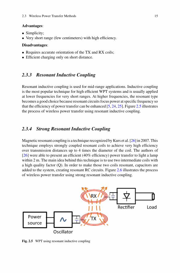
Resonant inductive coupling is used for mid-range applications. Inductive couplingis the most popular technique for high efficient WPT systems and is usually appliedat lower frequencies for very short ranges. At higher frequencies, the resonant typebecomes a good choice because resonant circuits focus power at specific frequency sothat the efficiency of power transfer can be enhanced [5, 24, 25]. Figure 2.5 illustratesthe process of wireless power transfer using resonant inductive coupling.
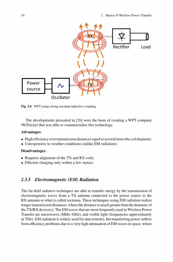
2.3.4 Strong Resonant Inductive Coupling
Magnetic resonant coupling is a technique recognized byKurs et al. [26] in 2007. Thistechnique employs strongly coupled resonant coils to achieve very high efficiencyover transmission distances up to 4 times the diameter of the coil. The authors of[26] were able to present an efficient (40% efficiency) power transfer to light a lampwithin 2 m. The main idea behind this technique is to use two intermediate coils witha high quality factor (Q). In order to make those two coils resonant, capacitors areadded to the system, creating resonant RC circuits. Figure 2.6 illustrates the processof wireless power transfer using strong resonant inductive coupling.
Rec fier Load
Powersource
Oscillator
TX
RX
Fig. 2.5 WPT using resonant inductive coupling
16 2 Basics of Wireless Power Transfer
Rec fier Load
Powersource
Oscillator
TX
RX
Fig. 2.6 WPT using strong resonant inductive coupling
The developments presented in [26] were the basis of creating a WPT company|WiTricity| that was able to commercialize this technology.
Advantages:
• Highefficiencyover transmissiondistances equal to several times the coil diameter;• Unresponsive to weather conditions (unlike EM radiation);
Disadvantages:
• Requires alignment of the TX and RX coils;• Efficient charging only within a few meters.
2.3.5 Electromagnetic (EM) Radiation
The far-field radiative techniques are able to transfer energy by the transmission ofelectromagnetic waves from a TX antenna connected to the power source to theRX antenna or what is called rectenna. These techniques using EM radiation realizelonger transmission distances,where the distance ismuch greater than the diameter ofthe TX/RX device(s). The EMwaves that aremost frequently used inWireless PowerTransfer are microwaves (MHz–GHz), and visible light (frequencies approximatelyin THz). EM radiation is widely used for data transfer, but transferring power suffersfrom efficiency problems due to a very high attenuation of EMwaves in space, where

2.3 Wireless Power Transfer Methods 17
the loss is usually inversely proportional to the square of the distance between TXand RX antennas [18].
Energy is transferred through the electric field of an electromagnetic wave, whichis radiative. Because of the safety matters raised by RF exposures, radiative wirelesscharging generally operates in a low-power region [27]. For example, omnidirectionalRF radiation is suitable only for sensor node applications with up to 10 mW powerconsumption [28, 29]. Systems based on light are mainly used directionally.
Advantages:
• Small receiver size;• Efficient power transfer over long distances specifically using directive radiations(microwave/laser).
Disadvantages:
• High losses of EM waves in the atmosphere;• For directional devices—requires complex tracking mechanisms and line of sight(LOS).
2.4 Implementation of Near-Field WPT Systems
This section discusses the recent developments and contributions in the non-radiativeWPT systems especially the inductive coupling, which is most popular due to theirsimplicity, high efficiency, and low cost. Inductive coupling systems can be mainlyclassified into two categories: magnetic induction and resonant inductive coupling.These systems, employing magnetic induction, transfer energy from a TX wind-ing coil to an RX winding coil using an alternating magnetic field [79, 80]. Thistechnology is usually suitable for short-range WPTs. On the other hand, mid-rangeWPT systems are usually implemented using electromagnetic resonant couplingtechnique. This technique uses resonance on both sending and receiving terminalsand has received a great amount of attention in recent years after being first presentedin 2007 by Kurs et al. [26]. This technique, developed by M. Soljacic and his team,utilized strongly coupled resonant circuits made of identical self-resonant helicalcoils of high quality factor to transfer power over a distance of 2 m achieving around40% efficiency as illustrated in Fig. 2.7 [26].
Figure 2.7 shows the experimental setup of strongly coupled magnetic resonancesimplemented by the MIT team [26].
Because of the simplicity and low cost of implementation, most of the existingWPT applications have embraced inductive coupling, or what is called InductivePower Transfer (IPT). IPT is capable of supporting high-power transfer above kilo-watt level, so it is commonly used in industrial automation applications [81], auto-mated underwater vehicles [82], electrical vehicles (EV) [83, 84], and high-speedtrains [85, 86].

18 2 Basics of Wireless Power Transfer
Fig. 2.7 Schematic of the experimental setup of strongly coupled magnetic resonances imple-mented by the MIT team [26]
The medium-power near-field charging (operating from several watts to tens ofwatts) are used for charging of medical implants and in daily applications. Wirelesscharging based on magnetic resonance coupling exhibits more powerful penetrationability especially for biomedical implants [4, 5, 80, 87]. The authors in [88] haveachieved, with a 3 cm TX coil and 2 cm RX coil, above 60% charging efficiencyover 2 cm distance.
The daily usage powering can be found in applications like portable electronicdevices and everyday devices (inductive toothbrush [89], TV [90], and lighting [91]).Regarding portable devices, the authors in [31] have reported the available differ-ent standard compliant wireless chargers, such as Energizer Qi charger, Verizon Qicharging pad, RAV Power’s Qi charger, ZENS Qi charging pad, Airpulse chargingpad, and Duracell Powermat, that have been commercialized to supply energy toportable devices [31].
Most of the WPT designs developed in the past decades were based on largewire wound coils, and several patterns of resonators that have been proposed formagnetically coupled resonance (MCR) WPT systems, such as helical and spiralresonators [92–94]. The disadvantages of theseMCR-WPT structures are their three-dimensional (3D) shape and their geometry (bulky) which are difficult to fabricate,and not suitable for charging small electronic devices like portable mobile phonesor biomedical implants.
In January 2014, M. Falavarjani and others reported a planar WPT system withsquare spiral resonators printed on the top and bottom layer of a single FR4 substrate,such that the printed spiral resonator is driven by the magnetic field of the coupling(feeding/load) loop [95]. The inductive coupled (feeding/load) loop is used to realizethe input/output matching network. The proposed WPT system in [95] achieved ameasuredWPT efficiency of 43% using TX/RX size of 12× 12 cm2 at a transmissiondistance of 10 cm.
2.4 Implementation of Near-Field WPT Systems 19
In August 2014, F. Jolani presented a magnetically coupled resonance WPT(MCR-WPT) system using printed spiral coil (PSC) resonators [96], where theTX/RX resonant coil and the feeding/load loop are printed on the same side ofan FR4 substrate to create a fully planar TX/RX coil set. The proposed WPT designin [96] with a two-turn PSC resonator and optimized geometric parameters achieveda maximumWPT efficiency of 77.27% at a transmission distance of 10 cm; with theparallel paths created with auxiliary strips, the effective series resistance (ESR) ofthe TX/RX PSC is decreased, the quality factor of the PSC resonators is improved,and the maximum WPT efficiency increased to 81.68% [96].
In January 2015, F. Jolani presented another highly efficient planar MCR-WPTsystem using two additional resonators for the TX and RX sides to increase thequality factor of the resonators [97]. Two substrates are stacked, where two PSCsare printed at the opposite sides of one substrate, and the third PSC is printed onthe bottom surface of the other substrate; and three PSC resonators are connectedto each other at the ends through vias [97]. To further improve the transmissionefficiency of the system, the outer edges of the multilayer resonator are connectedtogether using shorting walls. The proposed planar MCR-WPT system in [97] withmultilayer resonators offers higher transfer efficiency than the conventional planarMCR-WPT system, where a WPT efficiency of 84% has been achieved using thestacked substrates.
By the end of 2014, a breakthrough technology, named magnetic MIMO (Mag-MIMO), has been introduced to perform multi-antenna beamforming based on mag-netic waves [31]. This technology has opened an area for the magnetic-field beam-forming research [31]. The authors in [98] presented Magnetic MIMO, a systemthat can charge portable devices at distances up to 40 cm irrespective of the device’sposition and orientation, while commercial chargers are limited to less than 10 cm[98]. Magnetic MIMO achieved this performance by adapting the wireless conceptof MIMO beamforming to concentrate the resonating magnetic field on the receiverdevice to maximize the power transfer efficiency. Magnetic MIMO does not requireanymodification to the phone and hence can be usedwith today’s phones by includingthe small receiver coil (and circuit) in an outer cover attached to the phone.
2.5 Implementation of Far-Field WPT Systems
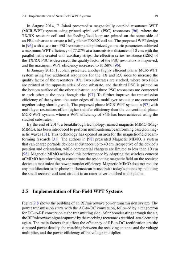
Figure 2.8 shows the building of an RF/microwave power transmission system. Thepower transmission starts with the AC-to-DC conversion, followed by a magnetronfor DC-to-RF conversion at the transmitting side. After broadcasting through the air,theRF/microwave signal capturedby the receiving rectenna is rectified into electricityagain. The main factors that affect the efficiency of RF-to-DC rectification are thecaptured power density, the matching between the receiving antenna and the voltagemultiplier, and the power efficiency of the voltage multiplier.

20 2 Basics of Wireless Power Transfer
Fig. 2.8 Far-field wireless charging [30]
Nikola Tesla was the first to perform experiments of wireless power transferbased on microwave technology. He focused on long-range wireless power transferand realized the transfer of microwave signals over a distance of about 48 km in1896 [32]. Another key step forward was accomplished in 1899 to transmit 100 MVof high-frequency electric power over a distance of 40 m to light 200 lamps [32].However, the technology that Tesla applied was put off because of the potentiallyharmful effects of emitting high voltages in electric arcs.
In 1964, W. Brown, the chief pioneer of practical wireless charging, used arectenna to convert microwaves to electricity. Brown demonstrated the practical-ity of microwave power transfer by powering a model helicopter [8]. Furthermore,the solar-powered satellite (SPS), that was presented in 1968, is another motivatingforce for long-range microwave power transfer [34]. The idea is to position hugesolar cells in geostationary earth orbit to collect sunlight energy. Electromagneticmicrowave beam is used to transmit energy back to earth. NASA’s project on SPSprompted great developments in microwave power transfer during the 1970s and1980s [31].
Far-field powering/charging systems can be implemented through either directive(beamforming) or non-directive radiation. Non-directive RF radiation techniques donot support line of sight, and they are less sensitive to the orientation or locationrelative to the transmitting antenna, so they are used in wireless power broadcasting.However, the resultant charging efficiency is relatively low. Low-power wireless sys-tems, such as wireless renewable sensor networks (WRSNs) and RFID systems arethe most embraced applications for non-directive charging [29, 31]. WRSNs withlow power consumption can keep a continuous operation with RF power densities inthe range of 20–200 μW/cm2 range [35]. The authors in [36] developed an ultra-lowpower sensor with far-field charging. The implemented transmitting and receivingsensor units consume only the power of 1.8 mW and 0.68 mW, respectively. Simi-lar wireless charging system designs for sensors that work with intentional wirelesscharger have been reported in [37–39]. Furthermore,wireless charging systems basedon ambient energy harvesting of RF/Microwave signals have also been developed. In[31], the authors reported the development of self-recharging sensors platform scav-enging environmental RF signals from TV broadcast [40, 41], amplitude-modulated

2.5 Implementation of Far-Field WPT Systems 21
(AM) radio broadcast [42, 43], mobile communications bands (900MHz/1800MHz)[44–46], WiFi routers [47, 48], and satellite communications [49–51].
Wireless RF-powered sensors are also used in applications such as wireless bodyarea networks (WBANs) [31]. WBANs are mainly categorized into implanted andwearable devices, and they have been reported in many articles [52, 53]. The powerconsumption of the wearable body sensors is tens of milliwatt, and the chargingefficiency is very small (for example 1.2% in [54]). A charging efficiency of smallerthan 0.1% was achieved for powering implanted sensors deeply inside body organs[55]. In [55–57], the authors have demonstrated biomedical implants that are poweredaway from tens of centimeters, with amicrowatt-level RF power source. RF-poweredsensors have also been used in the Internet of Things (IoT) applications [58, 59], andmachine-to-machine (M2M) communication systems [60].
Directive RF beamforming is employed to provide larger power consumptionfor wireless charging of electronic devices. Delivering high power across long dis-tance, throughmicrowavebeamforming techniques, has beenoffered in the 1960s and1970s. In 1975 [61],WilliamC. Brown presented themeasured and calculated resultsfor transporting electric power from one point to another via a wireless free spaceradiated microwave beam at 2.45 GHz. Far-field microwave beamforming has alsodriven the development of enormouswireless charging systems, such as SPS [62–64],microwave-driven unmanned vehicles [65, 66], Raytheon Airborne Microwave Plat-form (RAMP) [33], and Stationary High Altitude Relay Program (SHARP) [12, 67].Throughout the last decade, directive RF beamforming has found its medium-powerapplications for charging electronic devices [31]. The commercialized Cota system[68] can offer power beam equal to 10 mwithout any directive transmission. Further-more, the RF power station (beacon) has been developed to power mobile handsetsthrough cellular networks [69, 70].
Concerning the recent contributions for the far-field (RF/microwave) energy trans-mission, we noticed that all researches have concentrated on three main aspects:increasing the power conversion efficiency (RF-to-DC) [35, 71, 72], human safetyconsiderations [73, 74], and decreasing the size of the receiver (rectennas) [75]. In2001 [76], Hagerty designed planar rectenna arrays using printed right-hand circularpolarization (RHCP) and left-hand circular polarization (LHCP) spirals loaded withSchottky diodes to support fully right-and left-hand circular polarized rectennas thatare able to capture all incident signals irrespective of their polarization. This designhas achieved a conversion efficiency of 45% using linearly polarized wave, and withpower densities of 1.5mW/cm2. In 2003 [77], B. Strassner, andK. Chang have devel-oped a 5.8-GHz circularly polarized dual-loop traveling-wave rectifying antenna forlow power-density wireless power transmission applications. The rectenna achieved82% RF-to-DC conversion efficiency at an input power density of 2 mW/cm2 at5.8 GHz using a low-profile band-reject filter to suppress the re-radiated secondharmonic.

22 2 Basics of Wireless Power Transfer
Yong Park and others, in 2005 [78], designed a rectenna with a microstripharmonic-rejecting circular sector antenna at 2.4GHz.As compared to a conventionalmicrostrip square patch antenna, the circular sector antenna exhibited high reflectioncoefficients at the second and the third harmonics generated by a diode. The rectennaintegratedwith circular sector antenna can remove the need for a low-pass filter (LPF)placed between the antenna and the diode, in addition to producing higher outputpower, with maximum power conversion efficiency of 77.8% at an input power of10 dBm. in 2011 [78], Harouni and others proposed a 2.45-GHz rectenna using acompact dual circularly polarized (DCP) patch antenna with an RF/DC power con-version. The DCP antenna is joined to a microstrip line by an aperture in the groundplane and comprises a bandpass filter for harmonic rejections. The dual polarizationswere achieved using two crossed slots etched on the ground plane. The maximumefficiency is 63% for a power density of 0.525 mW/cm2. In 2015 [75], H. Visser hasdemonstrated a rectenna designed by neglecting the matching network and directlyconjugate impedance matching the antenna to the rectifier. The power conversionefficiency (PCE) has been increased, and the rectenna size was reduced, as it wasdemonstrated with a prototype with a PCE of 55% for a −10 dBm RF input power.
Table 2.1 summarizes the different implementation techniques of wireless powertransmission using the near-field (inductive/capacitive) coupling techniques and thefar-field (RF/microwaves/laserbeams) radiative techniques.
Table 2.1 Comparison between the different implementation methods of WPT systems
Technology Range Frequency Antenna type Applications
Inductive coupling Short Hz–MHz 3D wire loops, helicalantennas
charging electricalvehicles and electrictooth brush
Resonant inductivecoupling
Mid MHz–GHz Tuned wire coils,printed resonantspirals
Charging portabledevices, biomedicalimplants, RFIDs,smartcards
Capacitive coupling Short KHz–MHz Electrodes Charging portabledevices, smartcards.
RF and Microwaves Long GHz Rectennas, phasedarrays
Solar power satellites,powering droneaircraft
Light waves Long THz Laser beams, lenses,Photocells
Powering droneaircraft usingphotovoltaic cellpanels
2.6 Frequency Selection 23
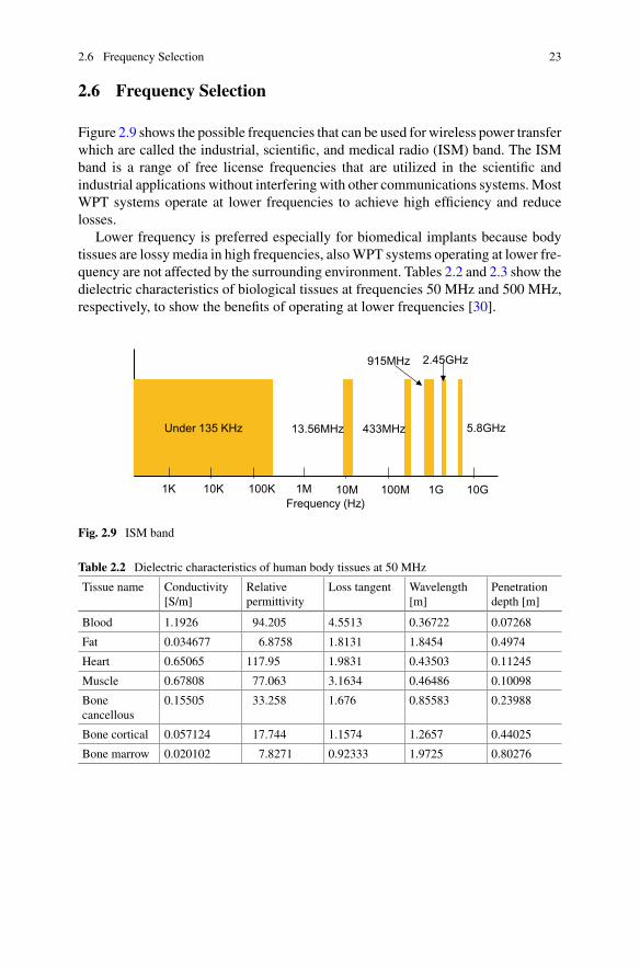
2.6 Frequency Selection
Figure 2.9 shows the possible frequencies that can be used for wireless power transferwhich are called the industrial, scientific, and medical radio (ISM) band. The ISMband is a range of free license frequencies that are utilized in the scientific andindustrial applications without interfering with other communications systems.MostWPT systems operate at lower frequencies to achieve high efficiency and reducelosses.
Lower frequency is preferred especially for biomedical implants because bodytissues are lossy media in high frequencies, alsoWPT systems operating at lower fre-quency are not affected by the surrounding environment. Tables 2.2 and 2.3 show thedielectric characteristics of biological tissues at frequencies 50 MHz and 500 MHz,respectively, to show the benefits of operating at lower frequencies [30].
Under 135 KHz
10K1K 100K 1M 10M 100M 1G 10G
13.56MHz 433MHz
915MHz
5.8GHz
2.45GHz
Frequency (Hz)
Fig. 2.9 ISM band
Table 2.2 Dielectric characteristics of human body tissues at 50 MHz
Tissue name Conductivity[S/m]
Relativepermittivity
Loss tangent Wavelength[m]
Penetrationdepth [m]
Blood 1.1926 94.205 4.5513 0.36722 0.07268
Fat 0.034677 6.8758 1.8131 1.8454 0.4974
Heart 0.65065 117.95 1.9831 0.43503 0.11245
Muscle 0.67808 77.063 3.1634 0.46486 0.10098
Bonecancellous
0.15505 33.258 1.676 0.85583 0.23988
Bone cortical 0.057124 17.744 1.1574 1.2657 0.44025
Bone marrow 0.020102 7.8271 0.92333 1.9725 0.80276

24 2 Basics of Wireless Power Transfer
Table 2.3 Dielectric characteristics of human body tissues at 500 MHz
Tissue name Conductivity[S/m]
Relativepermittivity
Loss tangent Wavelength[m]
Penetrationdepth [m]
Blood 1.3834 63.257 0.78622 0.07073 0.032531
Fat 0.042793 5.5444 0.27748 0.25227 0.29486
Heart 1.02 64.039 0.5726 0.072225 0.043208
Muscle 0.82245 56.445 0.52383 0.077352 0.050033
Bonecancellous
0.25397 21.95 0.41597 0.1254 0.099945
Bone cortical 0.10047 12.946 0.27901 0.16507 0.19192
Bone marrow 0.031217 5.619 0.19973 0.2517 0.4051
2.7 Overview of Commercial Products Supporting WPT
Applications using WPT technology have been most noticeable in the consumerelectronics market, where wireless charging promises to deliver new levels of con-venience for charging of everyday devices. In the 1990s, commercialized wirelesscharging products began to emerge due to thewidespread usage of portable electronicdevices [99]. Over the two past decades, many industrial organizations have initiatedactivities to develop standards and specifications correlated to the commercializa-tion and the implementation of WPT. The Society of Automotive Engineers (SAE)has a committee developing recommendations and eventually a standard for wire-less charging of electric vehicles. Furthermore, a number of industrial organizationshave been established to develop specifications for WPT systems and their com-ponents (e.g., Power Matters Alliance (PMA), Wireless Power Consortium (WPC),and Alliance for Wireless Power (A4WP)) [20] as summarized in Table 2.4 [17, 100,101].
Both far-field and near-field wireless charging approaches are experiencing devel-opments. In 2007, a research team, led by Prof. Marin Soljacic, proposed WiTricity
Table 2.4 Wireless power transfer standards
Standard
Frequency 6.78 MHz ~100–205 kHz ~201–315 kHz
Power 6.5 W 5 W 5 W
Coupling Loose < 50 mmResonance
Tight < 5 mmInductive
Tight < 5 mmInductive
Communicationsand powercontrol
Bluetooth In-band In-band

2.7 Overview of Commercial Products Supporting WPT 25
PowerTransmi er Mobile devices
Above ceilings orinaccessible places
Behind walls
Sensi ve or hazardous areas
Fig. 2.10 Powercast wireless charging system a Transmitter. b Receiver. c Wireless rechargeablesensor system
technology which verified through experimentations that mid-range non-radiativewireless charging is very efficient and practical. Furthermore, radiative wirelesscharging systems like Cota system [102], PRIMOVE [102], and Powercast wirelessrechargeable sensor system [103] (shown in Fig. 2.10) have been commercialized.
A survey regarding the current companies operating in the field of wireless charg-ing, energy harvesting, andwireless power transfer, yielded the following companies:
1. PowermatThis company was founded in 2006. Its first products were launched in 2009 [104].The wireless charger uses a “ring” coil that can attach to a smartphone or tablet.Charging begins once the ringed device is placed on a mat (charging pad) [104].
2. PowerByProxiThis company was founded in 2007, and they specialized in wireless charging forsmartphones and tablets, wearable devices, and industrial applications [105]. Thecompany depends on transmitting electrical currents from charging platform to thereceiving device wirelessly so that the electronic device stays charged without theneed to use an outlet again.
3. WiTricity/Wireless Power Consortium (WPC)WiTricitywas founded in 2007 to commercialize a new technology forwireless powertransfer using strong resonant inductive coupling that was invented and patented by ateam fromMassachusetts Institute of Technology (MIT). WiTricity or what is calledlater Wireless Power Consortium is a very big organization that adopted standard-ization and commercialization of WPT technology. As a result, the Qi standard hasemerged in 2009 [17, 106]. Qi provides wireless charging for over 300 products [17].A Qi wireless charger can power any Qi device. It relies on the magnetic resonant

26 2 Basics of Wireless Power Transfer
coupling between the transmitting coil in the charging pad and the receiving coil ina Qi device.
4. Mojo MobilityIt was founded in 2005 and they are interested in developing wireless chargingtechnologies for products like wearable electronics, mobile phones, and even high-power electric vehicle charging [107]. One of the advantages of this product is that itcan charge several devices simultaneously anyplace on the charging pad, contrastingother products that can charge only one device, and only if the device is locatedaccurately.
5. WiPower/QualcommWiPower is thewireless solution being developed byQualcomm through theAlliancefor Wireless Power Standard [108]. Qualcomm is advertising the wireless chargingtechnology to power your smartphone, lamps, wireless keyboards and mice, anddigital cameras. In 2012, Qualcomm co-founded the Alliance for Wireless Power,supporting the evolution of wireless power technology, products, and services, inaddition to launching a global standardization for wireless power transfer (Rezencebrand) [108].
6. OssiaIt was founded in 2013, and they developed a new technology entitled “Cota” thatdeliver remote, targeted energy to devices safely and intelligently [68]. Cota wirelesscharger can charge a mobile device up to 12 m away without requiring a direct line ofsight. The technology can even penetrate through walls and doors to power a device.
7. EnergousEnergous Corporation, founded in 2012, is the developer of WattUp wire-free charg-ing system. WattUp is a revolutionary radio-frequency (RF)-based charging solutionthat delivers smart mountable power via radio bands, like WiFi access points [109].
References
1. S. Aldhaher, Design and optimization of switched-mode circuits for inductive links. Ph.D.thesis, Cranfield University, Bedford, U.K., 2014
2. S. He, J. Chen, F. Jiang, D.K. Yau, G. Xing, Y. Sun, Energy provisioning in wireless recharge-able sensor networks. IEEE Trans. Mob. Comput. 12(10), 1931–1942 (2013)
3. S.J. Thomas, R.R. Harrison, A. Leonardo, M.S. Reynolds, A battery-free multichannel digitalneural/emg telemetry system for flying insects. IEEE Trans. Biomed. Circuits Syst. 6(5),424–436 (2012)
4. M. Zargham, P.G. Gulak, A 0.13μmCMOS integratedwireless power receiver for biomedicalapplications, in 2013 Proceedings of the ESSCIRC (ESSCIRC), (2013), pp. 137–140
5. R.-F. Xue, K.-W. Cheng, M. Je, High-Efficiency wireless power transfer for biomedicalimplants by optimal resonant load transformation. IEEE Trans. Circuits Syst. Regul. Pap.60(4), 867–874 (2013)
6. M.G. Golinski, Designing efficient wireless power transfer networks (Delft University ofTechnology, TU Delft, 2015)

References 27
7. N. Tesla, System of electric engineering, U.S. Patent No. 454,6228. W.C. Brown, Experimental airborne microwave supported platform, DTIC Document, 19659. W.C. Brown, R.H. George, N.I. Heenan, R.C. Wonson, Microwave to DC converter, U.S.
Patent No. US3434678A10. W.C. Brown, The history of power transmission by radio waves. IEEE Trans. Microw. Theory
Tech. 32(9), 1230–1242 (1984)11. W.C. Brown, The solar power satellite as a source of base load electrical power. IEEE Trans.
Power Appar. Syst. 6, 2766–2774 (1981)12. G. W. Jull, A. Lillemark, R. M. Turner, SHARP (stationary high altitude relay platform)
telecommunications missions and systems, in GLOBECOM’85-Global TelecommunicationsConference, vol. 1, (1985), pp. 955–959
13. NASA—NASAResearch Team Successfully Flies First Laser-Powered Aircraft. http://www.nasa.gov/vision/earth/improvingflight/laser_plane.html. Accessed 04 June 2016
14. M. Hutin, Transformer system for electric railways, U.S. Patent No. US527857A15. M. Cardullo, W. Parks, Transponder apparatus and system, U.S. Patent No. US3713148A16. A.R. Koelle, S.W. Depp, R.W. Freyman, Short-range radio-telemetry for electronic identifi-
cation, using modulated RF backscatter (Los Alamos Scientific Lab, NM, 1975)17. Wireless Power Consortium. https://www.wirelesspowerconsortium.com/. Accessed 04 Jun
201618. C.A. Balanis, Antenna Theory: Analysis and Design. (Wiley, 2016)19. S. Jalali Mazlouman, A. Mahanfar, B. Kaminska, Mid-range wireless energy transfer using
inductive resonance for wireless sensors, in IEEE International Conference on ComputerDesign, 2009. ICCD 2009, 2009, pp. 517–522
20. M.Kesler,HighlyResonantWireless Power Transfer: Safe, Efficient, and overDistance (2013)21. M. Kline, I. Izyumin, B. Boser, S. Sanders, Capacitive power transfer for contactless charging,
in 2011 Twenty-Sixth Annual IEEE Applied Power Electronics Conference and Exposition(APEC), (2011), pp. 1398–1404
22. A. Rozin, G.Kaplun, Capacitively coupled bi-directional data and power transmission system,US5847447 A (1998)
23. A.M. Sodagar, P. Amiri, Capacitive coupling for power and data telemetry to implantablebiomedical microsystems, in Neural Engineering, 2009. NER’09. 4th InternationalIEEE/EMBS Conference on, (2009), pp. 411–414
24. B.L. Cannon, J.F. Hoburg, D.D. Stancil, S.C. Goldstein, Magnetic resonant coupling as apotential means for wireless power transfer to multiple small receivers. IEEE Trans. PowerElectron. 24(7), 1819–1825 (2009)
25. O. Jonah, S.V.Georgakopoulos,Wireless power transmission to sensors embedded in concretevia magnetic resonance, in Wireless and Microwave Technology Conference (WAMICON),2011 IEEE 12th Annual, (2011), pp. 1–6
26. A. Kurs, A. Karalis, R. Moffatt, J.D. Joannopoulos, P. Fisher, M. Soljacic, Wireless powertransfer via strongly coupled magnetic resonances. Science, 317(5834), 83–86 (2007)
27. C.S. Branch, Limits of human exposure to radiofrequency electromagnetic energy in thefrequency range from 3 kHz to 300 GHz. Safe Code, 6 (2009)
28. L. Xie, Y. Shi, Y.T. Hou, A. Lou,Wireless power transfer and applications to sensor networks.IEEE Wirel. Commun. 20(4), 140–145 (2013)
29. A.P. Sample, D.J. Yeager, P.S. Powledge, A.V. Mamishev, J.R. Smith, Design of an RFID-based battery-free programmable sensing platform. IEEE Trans. Instrum. Meas. 57(11),2608–2615 (2008)
30. Dielectric Properties of Body Tissues: HTML clients. http://niremf.ifac.cnr.it/tissprop/htmlclie/htmlclie.php. Accessed 23 July 2016
31. X. Lu, P. Wang, D. Niyato, D.I. Kim, Z. Han, Wireless charging technologies: fundamentals,standards, and network applications. IEEE Commun. Surv. Tutor. 18(2), 1413–1452 (2016)
32. N. Tesla, Apparatus for transmitting electrical energy, U.S. Patent No. US1119732A33. B. Strassner, K. Chang, Microwave power transmission: historical milestones and system
components. Proc. IEEE 101(6), 1379–1396 (2013)

28 2 Basics of Wireless Power Transfer
34. J.O. McSpadden, J.C. Mankins, Space solar power programs and microwave wireless powertransmission technology. IEEE Microw. Mag. 3(4), 46–57 (2002)
35. Z. Popovic, E.A. Falkenstein, D. Costinett, R. Zane, Low-power far-field wireless poweringfor wireless sensors. Proc. IEEE 101(6), 1397–1409 (2013)
36. Y.-J. Hong, J. Kang, S.J. Kim, S.J. Kim, U.-K. Kwon, Ultra-low power sensor platformwith wireless charging system, in Circuits and Systems (ISCAS), 2012 IEEE InternationalSymposium on, (2012), pp. 978–981
37. S. Percy, C. Knight, F. Cooray, K. Smart, Supplying the power requirements to a sensornetwork using radio frequency power transfer. Sensors 12(12), 8571–8585 (2012)
38. C. Cato, S. Lim, UHF far-field wireless power transfer for remotely powering wireless sen-sors, in Antennas and Propagation Society International Symposium (APSURSI), 2014 IEEE,(2014), pp. 1337–1338
39. N. Shinohara, T. Ichihara, Coexistence of wireless power transfer via microwaves and wire-less communication for battery-less ZigBee sensors, in Electromagnetic Compatibility, Tokyo(EMC’14/Tokyo), 2014 International Symposium on, (2014), pp. 445–448
40. H. Nishimoto, Y. Kawahara, T. Asami, Prototype implementation of ambient RF energyharvesting wireless sensor networks, in Sensors, 2010 IEEE, (2010), pp. 1282–1287
41. R. Vyas, B. Cook, Y. Kawahara,M. Tentzeris, A self-sustaining, autonomous, wireless-sensorbeacon powered from long-range, ambient, RF energy, in Microwave Symposium Digest(IMS), 2013 IEEE MTT-S International, (2013), pp. 1–3
42. T. Sogorb, J.V. Llario, J. Pelegri, R. Lajara, J. Alberola, Studying the feasibility of energyharvesting from broadcast RF station for WSN, (2008), pp. 1360–1363
43. X.Wang,A.Mortazawi,High sensitivityRF energy harvesting fromAMbroadcasting stationsfor civilian infrastructure degradation monitoring, inWireless Symposium (IWS), 2013 IEEEInternational, (2013), pp. 1–3
44. L.M. Borges et al., Design and evaluation of multi-band RF energy harvesting circuits andantennas for WSNs, in Telecommunications (ICT), 2014 21st International Conference on,(2014), pp. 308–312
45. T.B. Lim, N.M. Lee, B.K. Poh, Feasibility study on ambient RF energy harvesting for wirelesssensor network, inMicrowaveWorkshop Series on RF andWireless Technologies for Biomed-ical and Healthcare Applications (IMWS-BIO), 2013 IEEE MTT-S International, (2013),pp. 1–3
46. M. Arrawatia, M.S. Baghini, G. Kumar, RF energy harvesting system from cell towers in900 MHz band, in Communications (NCC), 2011 National Conference on, (2011), pp. 1–5
47. E.A. Kadir, A.P. Hu, M. Biglari-Abhari, K.C. Aw, IndoorWiFi energy harvester with multipleantenna for low-power wireless applications, in Industrial Electronics (ISIE), 2014 IEEE 23rdInternational Symposium on, (2014), pp. 526–530
48. F. Alneyadi, M. Alkaabi, S. Alketbi, S. Hajraf, R. Ramzan, 2.4 GHz WLAN RF energyharvester for passive indoor sensor nodes, in Semiconductor Electronics (ICSE), 2014 IEEEInternational Conference on, (2014), pp. 471–474
49. A. Takacs, H. Aubert, L. Despoisse, S. Fredon, Microwave energy harvesting for satelliteapplications. Electron. Lett. 49(11), 722–724 (2013)
50. A. Takacs, H. Aubert, L. Despoisse, S. Fredon, Design and implementation of a rectenna forsatellite application, inWireless Power Transfer (WPT), 2013 IEEE, (2013), pp. 183–186
51. A. Takacs, H. Aubert, S. Fredon, L. Despoisse, K-band energy harvesting circuits for satelliteapplication, inMicrowave Conference (EuMC), 2013 European, (2013), pp. 991–994
52. F. Zhang, S.A. Hackwoth, X. Liu, C. Li, M. Sun, Wireless power delivery for wearablesensors and implants in body sensor networks, inEngineering inMedicine andBiology Society(EMBC), 2010 Annual International Conference of the IEEE, (2010), pp. 692–695
53. W.Y. Toh, Y.K. Tan, W.S. Koh, L. Siek, Autonomous wearable sensor nodes with flexibleenergy harvesting. IEEE Sens. J. 14(7), 2299–2306 (2014)
54. N. Desai, J. Yoo, A.P. Chandrakasan, A scalable, 2.9 mW, 1Mb/s e-textiles body area networktransceiver with remotely-powered nodes and bi-directional data communication. IEEE J.Solid-State Circuits 49(9), 1995–2004 (2014)

References 29
55. S. Majerus, S.L. Garverick, M.S. Damaser, Wireless battery charge management forimplantable pressure sensor, in Circuits and Systems Conference (DCAS), 2014 IEEE Dallas,(2014), pp. 1–5
56. E.Y. Chow, C.-L. Yang, Y. Ouyang, A.L. Chlebowski, P.P. Irazoqui, W.J. Chappell, Wire-less powering and the study of RF propagation through ocular tissue for development ofimplantable sensors. IEEE Trans. Antennas Propag. 59(6), 2379–2387 (2011)
57. M.Arsalan,M.H.Ouda, L.Marnat, T.J.Ahmad,A. Shamim,K.N. Salama,A5.2GHz, 0.5mWRF powered wireless sensor with dual on-chip antennas for implantable intraocular pressuremonitoring, inMicrowave SymposiumDigest (IMS), 2013 IEEEMTT-S International, (2013),pp. 1–4
58. Y.-K. Chen, Challenges and opportunities of internet of things, in Design Automation Con-ference (ASP-DAC), 2012 17th Asia and South Pacific, (2012), pp. 383–388
59. S. Gollakota, M.S. Reynolds, J.R. Smith, D.J. Wetherall, The emergence of RF-poweredcomputing. Computer 47(1), 32–39 (2014)
60. D.W.K. Ng, R. Schober, Energy-efficient power allocation for M2 M communications withenergy harvesting transmitter, in Globecom Workshops (GC Wkshps), 2012 IEEE, (2012),pp. 1644–1649
61. R.M. Dickinson, W.C. Brown, Radiated microwave power transmission system efficiencymeasurements, 1975
62. P.E. Glaser, The potential of satellite solar power. Proc. IEEE 65(8), 1162–1176 (1977)63. W.C. Brown, E.E. Eves, Beamed microwave power transmission and its application to space.
IEEE Trans. Microw. Theory Tech. 40(6), 1239–1250 (1992)64. R.H. Nansen, Wireless power transmission: the key to solar power satellites. IEEE Aerosp.
Electron. Syst. Mag. 11(1), 33–39 (1996)65. J. Miyasaka et al., Control for microwave-driven agricultural vehicle: tracking system of
parabolic transmitting antenna and vehicle rectenna panel—. Eng. Agric. Environ. Food 6(3),135–140 (2013)
66. J. Miyasaka et al., Development of an electric vehicle by microwave power transmission:development of small model vehicle and control of rectenna panel. Eng. Agric. Environ. Food7(2), 103–108 (2014)
67. T.W. East, A self-steering array for the SHARP microwave-powered aircraft. IEEE Trans.Antennas Propag. 40(12), 1565–1567 (1992)
68. http://www.ossiainc.com69. K. Huang, V.K. Lau, Enabling wireless power transfer in cellular networks: architecture,
modeling and deployment. IEEE Trans. Wirel. Commun. 13(2), 902–912 (2014)70. M. Erol-Kantarci, H.T. Mouftah, Radio-frequency-based wireless energy transfer in LTE-A
heterogenous networks, in Computers and Communication (ISCC), 2014 IEEE Symposiumon, (2014), pp. 1–6
71. C.R. Valenta, G.D. Durgin, Harvesting wireless power: survey of energy-harvester conversionefficiency in far-field, wireless power transfer systems. IEEE Microw. Mag. 15(4), 108–120(2014)
72. M. Xia, S. Aissa, On the efficiency of far-field wireless power transfer. IEEE Trans. SignalProcess. 63(11), 2835–2847 (2015)
73. S. Code, 6, Limits of human exposure to radiofrequency electromagnetic fields in the fre-quency range from 3 kHz to 300 GHz, Environ. Health Dir. Health Prot. Branch Health Can.Can., (1999)
74. C. Liu, Y.-X. Guo, H. Sun, S. Xiao, Design and safety considerations of an implantablerectenna for far-field wireless power transfer. IEEE Trans. Antennas Propag. 62(11),5798–5806 (2014)
75. H.J. Visser, S. Keyrouz, A.B. Smolders, Optimized rectenna design. Wirel. Power Transf.2(01), 44–50 (2015)
76. J.A. Hagerty, Z. Popovic, An experimental and theoretical characterization of a broadbandarbitrarily-polarized rectenna array, in Microwave Symposium Digest, 2001 IEEE MTT-SInternational, vol. 3, (2001), pp. 1855–1858

30 2 Basics of Wireless Power Transfer
77. B. Strassner, K. Chang, 5.8-GHz circularly polarized dual-rhombic-loop traveling-wave rec-tifying antenna for low power-density wireless power transmission applications. IEEE Trans.Microw. Theory Tech. 51(5), 1548–1553 (2003)
78. J.-Y. Park, S.-M. Han, and others, A rectenna design with harmonic-rejecting circular-sectorantenna. IEEE Antennas Wirel. Propag. Lett. 3(1), 52–54 (2004)
79. C.-J. Chen, T.-H. Chu, C.-L. Lin, Z.-C. Jou, A study of loosely coupled coils for wirelesspower transfer. IEEE Trans Circuits Syst. II Express Briefs 57(7), 536–540 (2010)
80. M. Zargham, P.G.Gulak,Maximumachievable efficiency in near-field coupled power-transfersystems. IEEE Trans. Biomed. Circuits Syst. 6(3), 228–245 (2012)
81. A. Kawamura, K. Ishioka, J. Hirai, Wireless transmission of power and information throughone high-frequency resonant AC link inverter for robot manipulator applications. IEEE Trans.Ind. Appl. 32(3), 503–508 (1996)
82. T. McGinnis, C.P. Henze, K. Conroy, Inductive power system for autonomous underwatervehicles, in OCEANS 2007, (2007), pp. 1–5
83. R. Severns, E. Yeow, G. Woody, J. Hall, J. Hayes, An ultra-compact transformer for a 100 Wto 120 kW inductive coupler for electric vehicle battery charging, in Applied Power Electron-ics Conference and Exposition, 1996. APEC’96. Conference Proceedings 1996., EleventhAnnual, vol. 1, (1996), pp. 32–38
84. J. Huh, S.W. Lee, W.Y. Lee, G.H. Cho, C.T. Rim, Narrow-width inductive power transfersystem for online electrical vehicles. IEEE Trans. Power Electron. 26(12), 3666–3679 (2011)
85. S. Lee et al., The optimal design of high-powered power supply modules for wireless powertransferred train, in Electrical Systems for Aircraft, Railway and Ship Propulsion (ESARS),2012, (2012), pp. 1–4
86. J.H. Kim et al., Development of 1-MW inductive power transfer system for a high-speed train.IEEE Trans. Ind. Electron. 62(10), 6242–6250 (2015)
87. A.K. RamRakhyani, S. Mirabbasi, M. Chiao, Design and optimization of resonance-basedefficient wireless power delivery systems for biomedical implants. IEEE Trans. Biomed.Circuits Syst. 5(1), 48–63 (2011)
88. D. Ahn, S. Hong, Wireless power transmission with self-regulated output voltage for biomed-ical implant. IEEE Trans. Ind. Electron. 61(5), 2225–2235 (2014)
89. M. Stratmann, P. Trawinski, Rechargeable toothbrushes with charging stations, U.S PatentNo. US20030085687A1
90. J. Kim, H.-C. Son, D.-H. Kim, Y.-J. Park, Optimal design of a wireless power transfer systemwith multiple self-resonators for an LED TV. IEEE Trans. Consum. Electron. 58(3) (2012)
91. D.W. Baarman, Inductively powered lamp assembly, U.S. Patent No. US6731071B292. M. Kiani, M. Ghovanloo, The circuit theory behind coupled-mode magnetic resonance-based
wireless power transmission. IEEE Trans. Circuits Syst. Regul. Pap. 59(9), 2065–2074 (2012)93. H. Hirayama, T. Amano, N. Kikuma, K. Sakakibara, An investigation on self-resonant and
capacitor-loaded helical antennas for coupled-resonant wireless power transfer. IEICE Trans.Commun. 96(10), 2431–2439 (2013)
94. X. Shi et al., Effects of coil shapes onwireless power transfer viamagnetic resonance coupling.J. Electromagn. Waves Appl. 28(11), 1316–1324 (2014)
95. M.M. Falavarjani,M. Shahabadi, J. Rashed-Mohassel,Design and implementation of compactWPT system using printed spiral resonators. Electron. Lett. 50(2), 110–111 (2014)
96. F. Jolani, Y. Yu, Z. Chen, A planar magnetically coupled resonant wireless power transfersystem using printed spiral coils. IEEE Antennas Wirel. Propag. Lett. 13, 1648–1651 (2014)
97. F. Jolani, Y. Yu, Z. Chen, Enhanced planar wireless power transfer using strongly coupledmagnetic resonance. Electron. Lett. 51(2), 173–175 (2015)
98. J. Jadidian, D. Katabi, Magnetic MIMO: how to charge your phone in your pocket, in Pro-ceedings of the 20th Annual International Conference on Mobile Computing and Networking,(2014), pp. 495–506
99. T.A. Vanderelli, J.G. Shearer, J.R. Shearer, Method and apparatus for a wireless power supply,U.S. Patent No. US7027311B2

References 31
100. R. Tseng, B. von Novak, S. Shevde, K.A. Grajski, Introduction to the alliance for wirelesspower loosely-coupled wireless power transfer system specification version 1.0, in WirelessPower Transfer (WPT), 2013 IEEE, (2013), pp. 79–83
101. J.I. Agbinya, Wireless Power Transfer, vol. 45. (River Publishers, 2015)102. http://primove.bombardier.com103. Powercast, www.powercastco.com104. Powermat, Wireless charging solutions, Powermat Life at 100%. http://www.powermat.com/.
Accessed 20 Apr 2017105. PowerbyProxi • Wireless power transfer & charging solutions, PowerbyProxi. https://
powerbyproxi.com/. Accessed 20 Apr 2017106. D. Van Wageningen, T. Staring, The Qi wireless power standard, in Power Electronics and
Motion Control Conference (EPE/PEMC), 2010 14th International, (2010), pp. S15–S25107. Mojo Mobility Technology. http://www.mojomobility.com/technology. Accessed 21 Apr
2017108. WiPower, Qualcomm, 12-Mar-2014. https://www.qualcomm.com/products/wipower.
Accessed 25 Mar 2017109. Energous—WattUp® Wire-Free Charging Technology

Chapter 3Wireless Power Transfer Using DGSs
3.1 Introduction
The recent rapid growth in wireless applications and the growing usage of consumerelectronic devices have radically augmented the market prospective for wirelesspower transfer (WPT) technology [1–13]. The growing demand forWPT technology,especially near-field coupling techniques, is motivated by wide-ranging applicationssuch as RFIDs [4], implanted medical devices [5–7], wireless buried sensors [8–11],and portable electronic devices [12, 13]. Moreover, near-field WPT is non-radiativeand is considered to be safe for health. Non-radiative techniques are based on induc-tive or capacitive coupling for short-range applications [14], and resonant inductivecoupling for mid-range applications [15]. Inductive coupling is the most widespreadtechnique for highly efficientWPT systems and is usually utilized at low frequencies.At high-frequency ranges, the resonant type becomes a good preference. Resonantcircuits concentrate more power at a definite frequency so that the power transferefficiency can be enhanced. On the other hand, strong resonant coupling usesmidwayresonators with high Q-factors to increase the WPT efficiency [10, 16].
Most of the transmitters and the receivers for magnetic resonant coupling WPTsystems were designed using 3D wired loops, spiral loops, or helical antennas[17–19]. Those coils are often massive in geometry and need accurate fabricationto keep high Q factor of the coil, which in sequence poses technical difficulties forthe WPT systems to be used in small electronic devices and implanted biomedicaldevices. On the other hand, other WPT systems have utilized printed spirals withsurface mounted (SMD) capacitors to get more compactness that are appropriatefor biomedical implants and board-to-board applications [20, 21]. Small footprintWPT systems can be designed using the printed spiral coils (PSCs) [22]. Most ofthe reported designs, to the best of our information, employed the printed spirals for
© Springer Nature Singapore Pte Ltd. 2019S. Hekal et al., Compact Size Wireless Power Transfer Using DefectedGround Structures, Energy Systems in Electrical Engineering,https://doi.org/10.1007/978-981-13-8047-1_3
33

34 3 Wireless Power Transfer Using DGSs
strong resonant coupling. To reduce the size, strongly coupled printed spirals wereoffered for the transmitting (TX) and receiving (RX) terminals, where inductivelycoupled feeds were used on each terminal to realize input/output impedance match-ing [22–25]. A five turns self-resonant printed spiral was used to achieve a WPTefficiency of 43.5% at a maximum transmission distance/
√bilateral area (h/D) of
0.83 [23]. In [24], supplementary strips have been added to decrease the ohmic resis-tance which in turn increased the quality factor and realized, at h/D = 1, a powertransfer efficiency of 81.7%. Furthermore,multilayer spiralswith shortingwallswereused to increase the Q factor and the mutual coupling [25], where an efficiency, ath/D = 1, of 84.4% was achieved. However, in [24, 25], the TX/RX spirals weredesigned on the same plane with the feed loops, and stacked substrates were stackedup to gather the inductance. In spite of the increased fabrication complexity in thestacked substrates, the available area for the inner loop is limited which limits fur-ther improvement of matching, mutual coupling and quality factor correspondingly.These systems, despite using high Q factor resonators, experience design complexityand restriction of transmission distance that does not exceed themaximumdimensionof the resonators.
Many microwave applications have employed the defected ground structures(DGSs) as quasi-lumped elements to implement low profiles of band-pass and band-stop filters (BSF) [26–29]. These compact structures have small sizes; which makethem appropriate to low-profile applications like portable electronic appliances andbiomedical implants. In the same manner, we can use capacitive loaded DGSs asbuilding blocks for WPT systems. In [30], comparison between different shapesof DGSs, used to get the same band rejection response, has been performed andthis study has proved that H-shaped DGS has the smallest size. The initial idea ofusing H-shaped DGSs for wireless power transmission has been illustrated in [31]by building H-shape resonators with an area of 25 × 25 mm2 to transfer power withtransmission efficiency of 80% at a distance of 5 mm at a frequency of 1 GHz. Thisdesign has then been improved using strong resonant coupling approach in [32] toaccomplish WPT efficiency of 70% at operational transmission distance of 9 mm at1.5 GHz. We investigate here systematic and asymmetric approaches of WPT sys-tem designs using different DGS resonators, driven by capacitive coupling. Differentshapes of DGS resonators (H, semi H, and spiral) are studied here with full-waveelectromagnetic (EM) analysis and circuit simulations at different frequency bands.An estimated quasi-static model depending upon the current distribution is used toextract equivalent circuits for these WPT systems. In this work, full-wave EM sim-ulator (High-Frequency Structures Simulator) for EM simulations, and Keysight’ADS for circuit analysis are used.

3.2 An Overview on Defected Ground Structures (DGS) 35
(a) (b) (c) (d)
(e) (f) (g)
Fig. 3.1 Different shapes ofDGSs. aCircular head dumbbell.bTriangular head dumbbell. c Squarehead dumbbell. d Spiral DGS. e Meander lines. f U-slot. g Square open-loop with a slot in middlesection
3.2 An Overview on Defected Ground Structures (DGS)
In recent years, there has been a growing interest in several new concepts that can beapplied to distributed (quasi-lumped) microwave circuits to meet the strict require-ments ofmodernmicrowave communication systems like highperformance, compactsize, and low cost [33]. One of these techniques is defected ground structure (DGS),where the metal ground plane of a microstrip (or strip line, or coplanar waveguide)circuit is intentionally modified to enhance performance [34]. The basic element ofDGS is etched periodic or nonperiodic cascaded resonant slots defected in the groundplane, placed directly under a transmission line, which perturb the shield current dis-tribution in the ground plane [33, 34]. This perturbation change characteristics ofthe transmission line such as line capacitance and inductance. In other words, anydefect etched in the ground plane of the microstrip can result in increasing the effec-tive capacitance and inductance. Figure 3.1 shows some of the resonant DGSs thatmay be used. Each one varies in occupied area, equivalent RLC circuit, couplingcoefficient, higher order responses, and other electrical parameters [34]. A user canchoose the structure that operates better for a particular application.
The design process, and the equivalent circuit extraction are challenging prob-lems for the efficient use of DGS. The equivalent circuit aids in applying a DGSto a practical circuit design, and in knowing the critical dimensions that affect thefrequency response of the DGS. The equivalent circuit elements (RLC) of DGS unitcan be extracted using the following methods:

36 3 Wireless Power Transfer Using DGSs
Fig. 3.2 Equivalent RLCcircuit of DGS unit
C
R
LZ0
Z0VS DGS unit
(a) Curve fitting of EM simulated S-parameters
In order to extract the equivalent circuit parameters of a DGS unit at the referenceplane, the scattering (S-) parameters versus frequency are calculated by EM sim-ulation to get the cutoff and central pole frequencies of the DGS response. Thenthe circuit elements for the derived equivalent circuit can be extracted by fitting theEM simulated S-parameters response for the one-pole Butterworth-type low-passresponse [35–37] using the formulas in [33]. The model shown in Fig. 3.2 com-prising a parallel R, L, and C resonant circuit connected to transmission lines at itsboth sides can be used to model effectively a DGS unit. The resistance correspondsto the radiation, conductor and dielectric losses in the defect. A physical vision ofthe working theory of DGS can be given knowing the correspondence between thephysical dimensions of DGS and the equivalent RLC parameters. The full-wave EManalysis do no assist in realizing this vision. The frequency response of DGS is notpredictable until the optimized solutions are achieved through iterative optimization.The conventional design and analysis method of DGSs is described using the flowchart shown in Fig. 3.3.
(b) Quasi-static modeling
The limitations of the above-mentioned curve fitting method can be overcome usingthismodelingmethod, as an equivalent circuitmodel, canbederived from thephysicaldimensions of the DGS. As can be seen in Fig. 3.4a of the DGS-disturbed microstriptransmission line, the return path of the current is fully perturbed and this currentis confined to the boundary of the perturbation, as shown in Fig. 3.4b, and returnsbelow the microstrip line once the perturbation is over [38]. The width of the sidefilament arms, which contributes to the inductance of the DGS, is determined, basedon the maximum concentration of the return current. The equivalent filament modelof the DGS is shown in Fig. 3.5. Hence, the equivalent circuit model is derived usingthe quasi-static expressions for microstrip bends, gaps, and crosses as explained indetails in [38]. The filament inductances for bends and straight lines are calculatedusing expressions found in [39–42]. This type of modeling clearly describes thephysical operation of DGS including how the DGS generates band-pass and band-stop responses and which dimensions affect significantly the performance [38].

3.2 An Overview on Defected Ground Structures (DGS) 37
Start
Select dielectric material (substrate), , thickness, metal thickness
Guess dimensions of the DGS
Perform full-wave EM analysis
Is the frequency response acceptable
Extract the equivalent circuit elements ( )
Stop
Yes
No
Change dimensions iteratively
Extract the EM simulated S-parameters vs. frequency
Fig. 3.3 Conventional design and analysis method of DGS
Fig. 3.4 Quasi-static modeling [38]. a Unit cell DGS. b Surface current on the ground plane
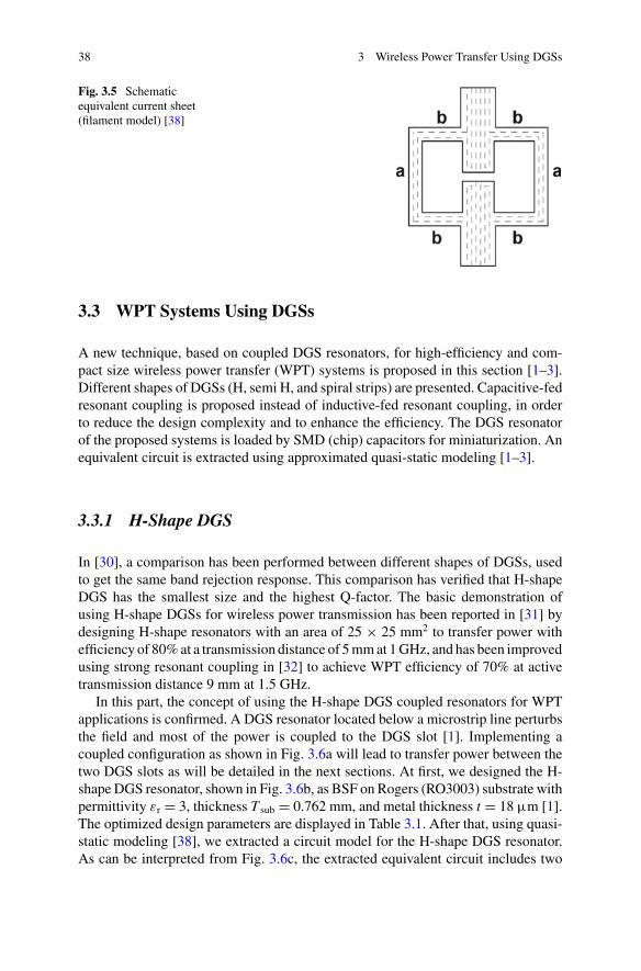
38 3 Wireless Power Transfer Using DGSs
Fig. 3.5 Schematicequivalent current sheet(filament model) [38]
3.3 WPT Systems Using DGSs
A new technique, based on coupled DGS resonators, for high-efficiency and com-pact size wireless power transfer (WPT) systems is proposed in this section [1–3].Different shapes of DGSs (H, semi H, and spiral strips) are presented. Capacitive-fedresonant coupling is proposed instead of inductive-fed resonant coupling, in orderto reduce the design complexity and to enhance the efficiency. The DGS resonatorof the proposed systems is loaded by SMD (chip) capacitors for miniaturization. Anequivalent circuit is extracted using approximated quasi-static modeling [1–3].
3.3.1 H-Shape DGS
In [30], a comparison has been performed between different shapes of DGSs, usedto get the same band rejection response. This comparison has verified that H-shapeDGS has the smallest size and the highest Q-factor. The basic demonstration ofusing H-shape DGSs for wireless power transmission has been reported in [31] bydesigning H-shape resonators with an area of 25 × 25 mm2 to transfer power withefficiency of 80%at a transmission distance of 5mmat 1GHz, and has been improvedusing strong resonant coupling in [32] to achieve WPT efficiency of 70% at activetransmission distance 9 mm at 1.5 GHz.
In this part, the concept of using the H-shape DGS coupled resonators for WPTapplications is confirmed. A DGS resonator located below a microstrip line perturbsthe field and most of the power is coupled to the DGS slot [1]. Implementing acoupled configuration as shown in Fig. 3.6a will lead to transfer power between thetwo DGS slots as will be detailed in the next sections. At first, we designed the H-shape DGS resonator, shown in Fig. 3.6b, as BSF on Rogers (RO3003) substrate withpermittivity εr = 3, thickness T sub = 0.762 mm, and metal thickness t = 18 μm [1].The optimized design parameters are displayed in Table 3.1. After that, using quasi-static modeling [38], we extracted a circuit model for the H-shape DGS resonator.As can be interpreted from Fig. 3.6c, the extracted equivalent circuit includes two

3.3 WPT Systems Using DGSs 39
90° 270°Top layer Bottom layer
50Port
50Port
h
CLP
CLS
P1 P1
P2P2
Wflsub
Wsub
d
WS
g
CLP
W
H
WH
lH
(a)
(b) (c)
Fig. 3.6 Hekal et al. [1] a Proposed coupled H-shape DGS resonators WPT system. b H-shapeDGS resonator as BSF at 300 MHz. c Simulated current distribution at phases (90°, and 270°)
parallel inductances L due to the two parallel rectangular loops of lengthH, widthW,and thickness d. Moreover, the equivalent circuit includes two parallel capacitances:the first capacitanceCg is because of the slot of length g andwidthWS, and the secondcapacitance CLP is due to the SMD chip capacitor. The equivalent circuit of H-shapeDGS resonator is exported from its physical dimensions where the inductance L iscalculated as (3.1) [42], the slot capacitance Cg as (3.2), and the resistance as (3.3).By substituting with the calculated design parameters from Table 3.1 in (3.1)–(3.3),we get the following equivalent circuit parameters L = 30 nH, R = 0.12 , Cg = 0.3pF that lead to LP= 15 nH, CP = Cg + CLP = 17.2 pF, Req = 0.06 . An equivalentcircuit model is shown in Fig. 3.7a. As shown in Fig. 3.7b, we have good agreementbetween circuit and EM simulated scattering (S-) parameters of the DGS-BSF, whichproves the offered equivalent circuit [1].

40 3 Wireless Power Transfer Using DGSs
Table 3.1 Design parameters of H-shape DGS resonator [1]
Dimension lsub W sub g WS lH WH H W d W f
Value (mm) 20 20 0.5 3 17 7 18.5 8.5 1.5 1.88
port50 Ω
port50 Ω
L R
L RCLP
Cg
CP
LP Req
(a)
(b)
Fig. 3.7 Verification of the quasi-static model for H-shape DGS. a Equivalent circuit [1]. b Com-parison between |S-parameters| of EM and circuit simulations [1]
L = e(W + H)
(0.0234
[log
(2WH
t + de
)− W
W + Hlog
[(W +
√W 2 + H 2
)e]
− H
W + Hlog
[(H +
√W 2 + H 2
)e]]
+ 0.01
[2
(√W 2 + H 2
W + H
)− 0.5 + 0.447
(t + d
W + H
)])μH, e = 39.37 (3.1)
Cg = 2Ws
πεoεre f f cosh
−1
(lHLs
)(3.2)
εre f f = εr + 1
2+ εr − 1
2
(1 + 12
(TsubW f
))− 12

3.3 WPT Systems Using DGSs 41
d
WS
g
CLP
W
H
WH
lH
Wf
lsub
Wsub
lstWst
Top layer Bo om layer
Stub
Feed line
lf
CLS
Fig. 3.8 PCB layout of H-shape DGS resonator for the proposed WPT system [1]
R = Rdct
δ(1 − e−t/ δ
)(1 + t
d
) (3.3)
As shown in the PCB outline of the single resonator in Fig. 3.8, the top layer is a50 microstrip line with length lf and width W f [1]. A stub loaded by capacitor isadded for impedance matching, which is easily represented by a series capacitanceCS calculated using (3.4). Where Z0 is the characteristic impedance of the stub andis adjusted by the stub width (Wst), β is the phase shift constant, lS = lst + lLS is thetotal equivalent length of the stub loaded capacitor, lst is the stub length and lLS =β−1 tan−1(ωZ0CLS) is the additional stub length added by the loading capacitor(CLS) [1].
CS = 1
ωZ0tan(βlS) (3.4)
If the stub length offers sufficient capacitance, no loading capacitor will berequired and the total length will reduce to lst . Most of the WPT structures, that usea strong resonant coupling, depend on inductive feed followed by resonant inductivecoupling; herewe use capacitive feed, realized by the stub-loaded capacitor, followedby resonant inductive coupling. The equivalent circuit model of the WPT system isshown in Fig. 3.9.
The proposedWPT system operating at 300MHz is fabricated using the designedparameters illustrated in Table 3.2 and Keysights’ vector network analyzer (PNAN5222A) was used in the measurements. In order to fix the distance between thetwo resonators, we insert a cuboid foam whose relative permittivity is 1.2. Themeasurement setups of the fabricated WPT systems using H-shape DGS resonators

42 3 Wireless Power Transfer Using DGSs
Fig. 3.9 An equivalentcircuit of the proposed WPTsystem using coupledH-shape DGS resonators [1]
LP
CP
LP
CPReq Req
CSCS
port50 Ω
port50 Ω
K
CPCP ReqReq
LPLP
port50 Ω
port50 Ω
Cst CstCLSCLS
K
are shown in Fig. 3.10. The chip capacitors used are fromMurata with package/case0402 (1 mm × 0.5 mm). It can be found that the measured |S-parameters| of theH-shape DGS resonators WPT system are in good agreement with the circuit andEM simulation results as shown in Fig. 3.11. The fabricated design on a RO3003substrate has a size of 20 × 20 mm2. The achieved transmission distance of h =13mm indicates the critical coupling. Themeasured and simulatedWPT systems areoptimized for a very insignificant return loss (|S11| < −20 dB); hence, the efficiencycan be simply calculated from the following formula |S21|2×100% and consequentlya 68% measured WPT efficiency is achieved at 300 MHz.
The following section intends to validate the proposed equivalent circuit, par-ticularly representation of the stub, and its title role for impedance matching. Thestub and its equivalent capacitance representation are shown in Fig. 3.12. From thecomparison of circuit and EM simulation results shown in Fig. 3.13a, b, it can beobserved that the stub is equivalent to a series capacitor, and it has a straight effecton the impedance matching and frequency adjustment.Misalignment StudyThis section investigates the dependability of theH-shapeDGS-WPT system throughanalysis of its performance with the different WPT critical factors (horizontal shiftand coaxial orientation misalignments) [1].Horizontal shift misalignmentThe misalignment between the TX and RX resonators due to a horizontal shift inX and Y directions, as shown in the L.H.S of Fig. 3.14a, is studied. The verticaltransmission distance is fixed at h = 13 mm. From the results shown in Fig. 3.14b,it can be noticed that the maximum power transfer efficiency is achieved at perfectalignment. A little decrease in the efficiency happens for the Y shift. However, ahuge degradation in the efficiency occurs at a shift of 7 mm for the X and X = Y
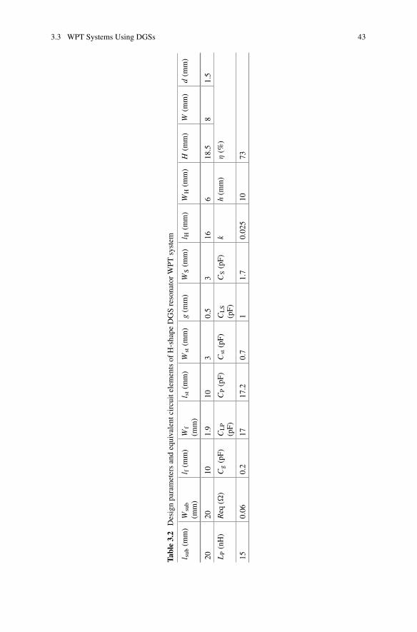
3.3 WPT Systems Using DGSs 43
Table3.2
Designparametersandequivalent
circuitelementsof
H-shape
DGSresonatorWPT
system
l sub
(mm)
Wsub
(mm)
l f(m
m)
Wf
(mm)
l st(m
m)
Wst(m
m)
g(m
m)
WS(m
m)
l H(m
m)
WH(m
m)
H(m
m)
W(m
m)
d(m
m)
2020
101.9
103
0.5
316
618.5
81.5
LP(nH)
Req
()
Cg(pF)
CLP
(pF)
CP(pF)
Cst(pF)
CLS
(pF)
CS(pF)
kh(m
m)
η(%
)
150.06
0.2
1717.2
0.7
11.7
0.025
1073

44 3 Wireless Power Transfer Using DGSs
13 mm
Fig. 3.10 Measurement setup of the fabricated WPT systems using H-shape DGS resonators [1]
-40
-35
-30
-25
-20
-15
-10
-5
0
285 290 295 300 305 310 315
|S-p
aram
eter
s| (d
B)
Frequency (MHz)
-5-4-3-2-1
295 300 305
MeasuredEM Sim.Circuit Sim.
|S21|
|S11|
Fig. 3.11 Comparison between the measured and the simulated |S-parameters| of the proposedWPT system using H-shape DGS resonators at 300 MHz and at transmission distance h = 13 mm[1]
shifts where the position of the maximum magnetic field of RX resonator faces aminimum magnetic field of the TX resonator.Coaxial orientation misalignmentWe study here the coaxial orientation’s effect of the RX resonator at different angleswith respect to the TX resonator as shown in the R.H.S of Fig. 3.14a. From the resultsshown in Fig. 3.14c, it can be found out that perfect orientation lead to the highestEM simulated WPT efficiency of 75% [1]. However, as the RX resonator rotates

3.3 WPT Systems Using DGSs 45
Fig. 3.12 3D schematicview of the proposed WPTsystem with therepresentation of the stub asa lumped capacitor [1]
around the z-axis, the WPT efficiency decayed to 50% at ±50° due to polarizationmisalignment [1]. Furthermore, the cross-polarization that takes place between thedriving and the load resonators at angle ±90° leads to a destructive coupling.
3.3.2 Semi H-Shape
In this section, a semi H-shape DGS resonator is presented as shown in Fig. 3.15.Considering the current distribution loops, the semi H-shape resonator consists ofonly one current loop which realizes a higher inductance than that of H-shape res-onator that consequently increases theWPTefficiency, and increases the transmissiondistance [1]. The PCB layout of semi H-shape DGS resonator is shown in Fig. 3.16a.The problem with the H-shape DGS resonator emerges from the value of the equiva-lent inductance of the two parallel loops. The equivalent inductance is half of one ofthem. In addition, the opposite direction of the current flow in these loops as shown inFig. 3.6c, is the reason for the degradation in the performance due to misalignmentsas explained earlier. The proposed semi H-shape DGS resonator with a half size ofthe H-shape doubles the inductance because of the existence of single loop [1].
The proposed structure for WPT is composed of two coupled semi H-shape DGSresonators set back to back as shown in Fig. 3.16b. The equivalent circuit of theproposed structure is shown inFig. 3.16c.Themutual inductancebetween twocoaxialidentical square loops can be determined from the sum of the mutual inductances ofthe parallel wires [43]. For two parallel square loops of side length “a” and separated

46 3 Wireless Power Transfer Using DGSs
-30
-25
-20
-15
-10
-5
0
-10
-8
-6
-4
-2
0
285 290 295 300 305 310 315
|S11
| (dB
)
|S21
| (dB
)
Frequency (MHz)
Cs=1.5pFCs=1.9pFCs=2.1pFCs=2.5pF
|S11|
|S21|
-30
-25
-20
-15
-10
-5
0
-10
-8
-6
-4
-2
0
285 290 295 300 305 310 315
|S11
| (dB
)
|S21
| (dB
)
Frequency (MHz)
Cs=1.5pFCs=1.9pFCs=2.1pFCs=2.5pF
|S11|
|S21|
(a)
(b)
Fig. 3.13 Representation of the stub as a lumped capacitor. a CST Simulated |S-parameters| [1].b ADS Simulated |S-parameters| [1]
by distance h, the mutual inductance, and the coupling coefficient can be calculatedusing (3.5), (3.6), respectively [20]. This design is implemented, approximately, withthe same size of the H-shape DGS-WPT system. The same substrate is used for bothdesigns. As a result, we get the following design parameters: lf = 10.5 mm, W f =1.88 mm, lst = 7 mm, W st = 2.5 mm, A = 21 mm, d = 1.8 mm, g = 0.2 mm, andthe circuit parameters: LP = 45 nH, CP = 5.2 pF, CS = 1.2 pF, LM = 1.1 nH, and k= 0.033.
LM = 2μ0
π
[a ln
(a + √
a2 + h2
h
)−
√a2 + h2 + h
+√2a2 + h2 −
√a2 + h2 − a ln
(a + √
2a2 + h2√a2 + h2
)](3.5)

3.3 WPT Systems Using DGSs 47
Fig. 3.14 Misalignment studies for H-shape DGS-WPT system (20 × 20 mm2). a Schematic ofmisalignment due to horizontal shift and orientation [1]. b EM simulated WPT efficiency versusmisalignment shifts [1]. c EM simulated WPT efficiency versus orientation angle [1]

48 3 Wireless Power Transfer Using DGSs
Semi H-shapeH-shape
Fig. 3.15 Schematic of semi H-shape DGS resonator [1]
A a
50 Ωport
50 Ωport CLS
CLP
d
lst
lfWf
Wst
g
LP
CP
LP
CPReq Req
CSCS
port50 Ω
K
port50 Ω
(a)
(b)
(c)
Fig. 3.16 The proposed WPT system based on semi H-shape DGS resonators [1]. a PCB layoutof a single resonator. b 3D schematic view. c equivalent circuit

3.3 WPT Systems Using DGSs 49
Table 3.3 Comparison between the optimum design parameters of H-shape and semi H-shapeDGS resonators and their WPT efficiency at 300 MHz
WPTsystem
Size(mm2)
R(Ω)
LP(nH)
LM(nH)
CP (pF) CS (pF) h(mm)
Meas. η(%)CLP Cg CLS Cst
H-shape 20 × 20 0.06 15 0.27 17 0.3 1.2 0.8 13 68
SemiH-shape
21 × 21 0.15 45 1.1 5 0.2 0.8 0.4 25 73
k = LM
LP(3.6)
In [44, 45], a method to predict the WPT system maximum obtainable efficiency(ηopt ) by means of a factor named U has been discussed. The U-factor and thecorresponding ηopt are calculated using (3.7) and (3.8), respectively. Table 3.3 showsa comparison between the optimum design parameters of theWPT systems using H-shapeDGS and semiH-shapeDGS resonators at 300MHz.Wediscuss the distinctionin the performance between the two structures in the following lines. As illustratedpreviously, the H-shape DGS is composed of two parallel loops. This configurationleads to lower losses than that of the semi H-shape DGS. However, the oppositeflow of the current in the H-shape DGS loops leads to a poor coupling performance;hence, themutual inductance is much lower than that of the semi H-shape DGS-WPTsystem. Consequently, the U-factor and ηopt of the H-shape DGS-WPT system havelower values than the same factors of the semi-H-shape DGS-WPT system with thesame size and separation distance.
U = kQ = ω0LM
R(3.7)
ηopt = U 2/(1 +
√1 +U 2
)2(3.8)
Table 3.3 shows a comparison between the optimum design parameters of theWPT systems using H-shape DGS and semi H-shape DGS resonators at 300 MHz.Figure 3.17 shows themagnetic field distribution of the proposed semi H-shapeWPTsystem at different phases (0°, 90°, 180°, and 270°).
Directly, the proposed WPT system using semi H- shape DGS resonators is fab-ricated with executing the optimum designed parameters described in Table 3.3.Keysights’ vector network analyzer PNA N5222A is used in the measurements. Inorder to fix the distance between the two resonators, we insert a cuboid foam withrelative permittivity 1.2. The measurement setups of the fabricated WPT systemusing semi H-shape DGSs are presented in Fig. 3.18. The used chip capacitors arefrom Murata Electronics with package/case 0402 (1 mm × 0.5 mm). The parasiticeffect of the used capacitor values (0.8 and 5 pF) is negligible at the desired operatingfrequency (300 MHz) [23]. It can be found that the measured |S-parameters| of the
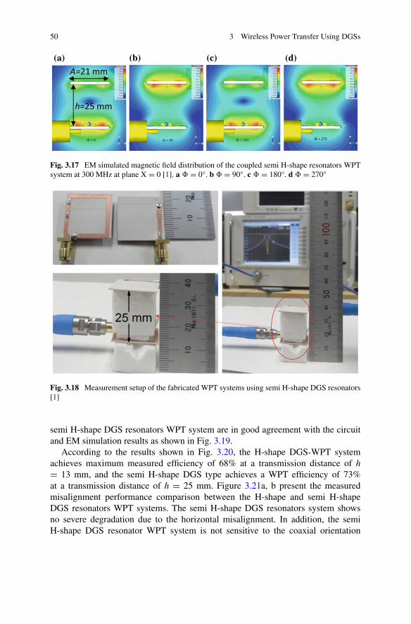
50 3 Wireless Power Transfer Using DGSs
A=21 mm
h=25 mm
(a) (b) (c) (d)
Fig. 3.17 EM simulated magnetic field distribution of the coupled semi H-shape resonators WPTsystem at 300 MHz at plane X = 0 [1]. a = 0°. b = 90°. c = 180°. d = 270°
Fig. 3.18 Measurement setup of the fabricated WPT systems using semi H-shape DGS resonators[1]
semi H-shape DGS resonators WPT system are in good agreement with the circuitand EM simulation results as shown in Fig. 3.19.
According to the results shown in Fig. 3.20, the H-shape DGS-WPT systemachieves maximum measured efficiency of 68% at a transmission distance of h= 13 mm, and the semi H-shape DGS type achieves a WPT efficiency of 73%at a transmission distance of h = 25 mm. Figure 3.21a, b present the measuredmisalignment performance comparison between the H-shape and semi H-shapeDGS resonators WPT systems. The semi H-shape DGS resonators system showsno severe degradation due to the horizontal misalignment. In addition, the semiH-shape DGS resonator WPT system is not sensitive to the coaxial orientation
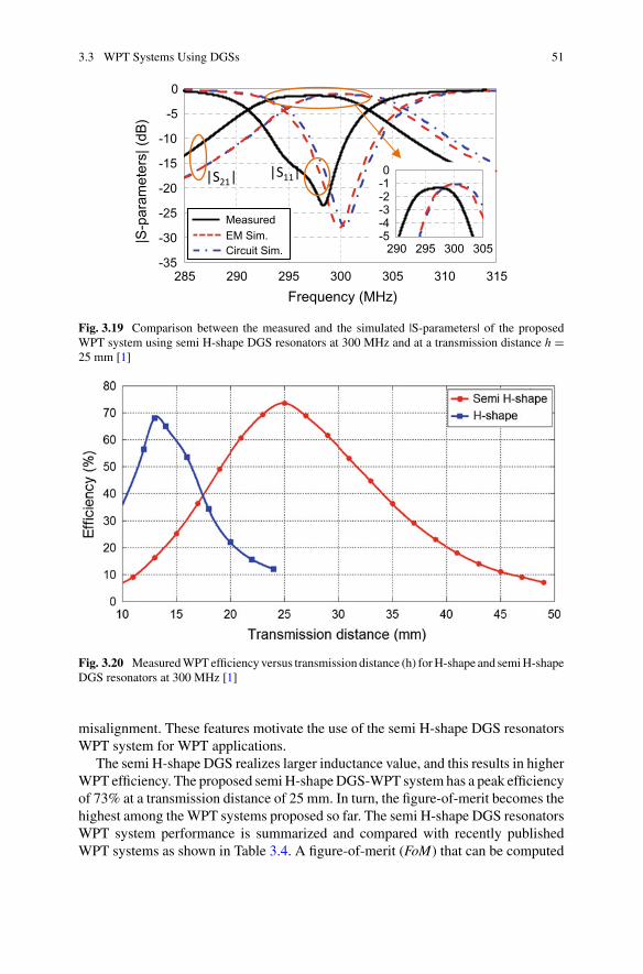
3.3 WPT Systems Using DGSs 51
-35
-30
-25
-20
-15
-10
-5
0
285 290 295 300 305 310 315
|S-p
aram
eter
s| (d
B)
Frequency (MHz)
MeasuredEM Sim.Circuit Sim.
|S21| |S11|
-5-4-3-2-10
290 295 300 305
Fig. 3.19 Comparison between the measured and the simulated |S-parameters| of the proposedWPT system using semi H-shape DGS resonators at 300 MHz and at a transmission distance h =25 mm [1]
Fig. 3.20 MeasuredWPTefficiency versus transmission distance (h) forH-shape and semiH-shapeDGS resonators at 300 MHz [1]
misalignment. These features motivate the use of the semi H-shape DGS resonatorsWPT system for WPT applications.
The semi H-shape DGS realizes larger inductance value, and this results in higherWPT efficiency. The proposed semiH-shapeDGS-WPT system has a peak efficiencyof 73% at a transmission distance of 25 mm. In turn, the figure-of-merit becomes thehighest among theWPT systems proposed so far. The semi H-shape DGS resonatorsWPT system performance is summarized and compared with recently publishedWPT systems as shown in Table 3.4. A figure-of-merit (FoM) that can be computed

52 3 Wireless Power Transfer Using DGSs
Fig. 3.21 Comparison between the measured power transfer efficiency versus misalignment [1]due a horizontal shift, and b different orientation angles for H-shape (20 × 20 mm2) and semiH-shape (21 × 21 mm2) DGS-WPT systems
using (3.9) is used to compare the performance [32]. The proposed design showsthe highest FoM. Besides, its WPT distance is about 1.2 times its resonators’ largestdimension.
FoM = η × h√Size
(3.9)
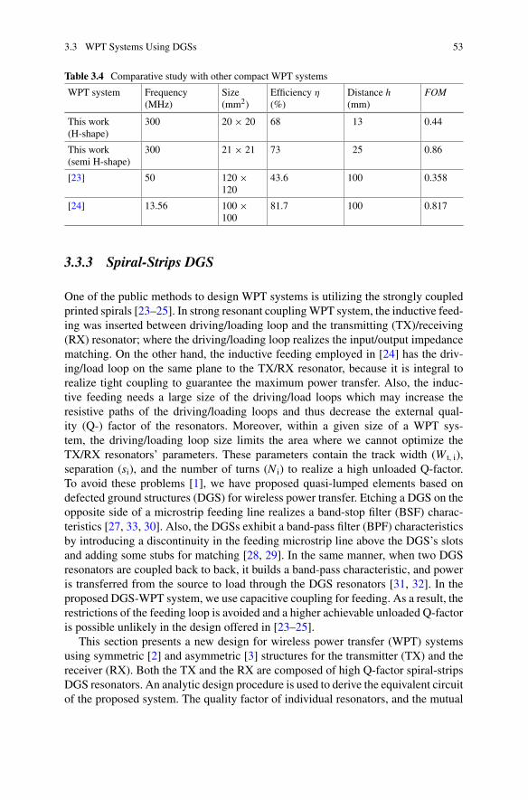
3.3 WPT Systems Using DGSs 53
Table 3.4 Comparative study with other compact WPT systems
WPT system Frequency(MHz)
Size(mm2)
Efficiency η
(%)Distance h(mm)
FOM
This work(H-shape)
300 20 × 20 68 13 0.44
This work(semi H-shape)
300 21 × 21 73 25 0.86
[23] 50 120 ×120
43.6 100 0.358
[24] 13.56 100 ×100
81.7 100 0.817
3.3.3 Spiral-Strips DGS
One of the public methods to design WPT systems is utilizing the strongly coupledprinted spirals [23–25]. In strong resonant couplingWPT system, the inductive feed-ing was inserted between driving/loading loop and the transmitting (TX)/receiving(RX) resonator; where the driving/loading loop realizes the input/output impedancematching. On the other hand, the inductive feeding employed in [24] has the driv-ing/load loop on the same plane to the TX/RX resonator, because it is integral torealize tight coupling to guarantee the maximum power transfer. Also, the induc-tive feeding needs a large size of the driving/load loops which may increase theresistive paths of the driving/loading loops and thus decrease the external qual-ity (Q-) factor of the resonators. Moreover, within a given size of a WPT sys-tem, the driving/loading loop size limits the area where we cannot optimize theTX/RX resonators’ parameters. These parameters contain the track width (W t, i),separation (si), and the number of turns (N i) to realize a high unloaded Q-factor.To avoid these problems [1], we have proposed quasi-lumped elements based ondefected ground structures (DGS) for wireless power transfer. Etching a DGS on theopposite side of a microstrip feeding line realizes a band-stop filter (BSF) charac-teristics [27, 33, 30]. Also, the DGSs exhibit a band-pass filter (BPF) characteristicsby introducing a discontinuity in the feeding microstrip line above the DGS’s slotsand adding some stubs for matching [28, 29]. In the same manner, when two DGSresonators are coupled back to back, it builds a band-pass characteristic, and poweris transferred from the source to load through the DGS resonators [31, 32]. In theproposed DGS-WPT system, we use capacitive coupling for feeding. As a result, therestrictions of the feeding loop is avoided and a higher achievable unloaded Q-factoris possible unlikely in the design offered in [23–25].
This section presents a new design for wireless power transfer (WPT) systemsusing symmetric [2] and asymmetric [3] structures for the transmitter (TX) and thereceiver (RX). Both the TX and the RX are composed of high Q-factor spiral-stripsDGS resonators. An analytic design procedure is used to derive the equivalent circuitof the proposed system. The quality factor of individual resonators, and the mutual

54 3 Wireless Power Transfer Using DGSs
H-shape Semi H-shape Spiral strips DGS
Di
CP,i
Wt,i
DiCP,i
Wt,i
CP,i
vias
Di
siWt,i
2Di Di Di
0
100
200
300
400
500
600
20 30 40 50 60 70
Self
Indu
ctan
ce (n
H)
Side length, Di (mm)
H-shapeSemi H-shapeSpiral-strips DGS
(a)
(b)
Fig. 3.22 Comparison between three different shapes ofDGS (H-shape, semiH-shape, spiral-stripsDGS) [2]. a Current distribution. b Computed self-inductance
coupling are analyzed to achieve high power transfer efficiency. As discussed earlierat the beginning of this chapter, one of the first applications of DGS resonators wasillustrated by the authors in [1], where two H-shape DGS resonators were coupledback to back to realize a WPT system, and power is transferred at a distance of3.5 mm only. First, reasons for the low power transfer distance were investigated, andspiral-strips DGSwas proposed to mitigate the problems in H-shape DGS resonatorsthat encountered in [31, 32] and provides more enhancements rather than the semiH-shape DGS resonators.
Figure 3.22a shows the H-shape DGS and its reformed versions (the semi H-shape, and the spiral-strips DGS) with the EM simulated current path, where thereare two parallel current paths in H-shape DGS. This results in low self-inductanceof the resonator which causes the lower efficiency at a larger distance [31, 32]. First,this problem is overcome by constructing a single current path only like in a SemiH-shape DGS resonator and the value of inductance is further improved as in Spiral-strips DGS resonator [2]. Figure 3.22b shows the calculated inductance of the threeDGS resonators, where the elongated current path in the spiral-strips DGS providestwice the self-inductance that of the semi H- shape and four times that of the H-shapeusing only half the area of H-shape DGS. Therefore, the spiral-strips DGS deliversthe uppermost Q-factor between the others, and they are employed in this work [2].

3.3 WPT Systems Using DGSs 55
Vias
Di
di
Wt,i si
Top layer Bottom layer
Microstripline
P2
P1
BridgeCP,iWf,i
50
50
50
50
-50
-40
-30
-20
-10
0
10 20 30 40 50 60 70 80 90 100
|S-p
aram
eter
s| (d
B)
Frequency (MHz)
|S21| HFSS|S11| HFSS|S21| ADS|S11| ADS
CP,i
RiLP,i
P1 P2
-50
-40
-30
-20
-10
0
10 20 30 40 50 60 70 80 90 100
|S-p
aram
eter
s| (d
B)
Frequency (MHz)
|S21| HFSS|S11| HFSS|S21| ADS|S11| ADS CP,i
Ri
LP,i
P1 P2
(a)
(b) (c)
Fig. 3.23 Proposed spiral-strips DGS resonator as BSF [2]. a PCB layout. b, c EM and circuitsimulated |S-parameters| embedded with equivalent circuit extracted by quasi-static modeling andanalogy with one-pole Butterworth BSF response, respectively
Figure 3.23a shows the PCB layout of the proposed spiral-strips DGS resonatoroperating as a band-stop filter (BSF). This DGS resonator has been designed onRogers substrate (RO5880) with permittivity εr = 2.2, thickness T sub = 0.5 mm, andmetal thickness t = 18 μm, where the top layer is 50 microstrip line of widthW f,i. Using the quasi-static modeling proposed in [38], the bottom layer (DGS)is represented by the printed spiral inductor of self-inductance (LP,i) with seriesresistance (Ri), which are calculated by (3.10) and (3.11), [46, 47], respectively.Where N i is the number of turns (in this work N i = 2), μ0 is the permeability offree space = 4π × 10−7 H/m, Di and di are the outer and the inner diameters, di =Di − 2si − 4W t,i, and ϕi is the fill factor, Rdc,i is the dc resistance, and δ is the skindepth. Figure 3.23b shows good agreement between the EM and circuit simulatedmagnitude of scattering parameters (|S-parameters|).

56 3 Wireless Power Transfer Using DGSs
LP,i = 1.27μ0N 2i Davg,i
2
[ln
(2.07
ϕi
)+ 0.18ϕi + 0.13ϕ2
i
]Henry, i = 1, 2 (3.10)
Davg,i = Di + di2
, φi = Di − diDi + di
Ri = Rdc,it
δ(1 − e−t/ δ
)(1 + t
Wt,i
), i = 1, 2 (3.11)
The corresponding RLC values of the suggested spiral-strips DGS, shown inFig. 3.23a, are also extracted by (3.12)–(3.14) [33] from its EM band reject response.Whereω0 is the center angular frequency of the stopband,ωc is the 3 dBcutoff angularfrequency taken from the S21 curve (shown in Fig. 3.23c), and Z0 = 50 .
CP,i = ωc
2Z0(ω20 − ω2
C
) Farad (3.12)
LP,i = 1
ω20CP
Henry (3.13)
Ri = 2Z0√1
|S11(ω)|2 −(2Z0(ωCP,i − 1
ωLP,i))2 − 1
(3.14)
Figure 3.23b shows the electromagnetic (EM) simulated magnitude of the scatter-ing parameters (|S-parameters|) performed using the high-frequency structure simu-lator (HFSS); this frequency response has been achieved using the design parameters(W f1 = 1.55 mm, D1 = 50 mm, d1 = 34 mm, W t1 = 3.5 mm, and s1 = 1 mm) thatgive LP1 = 315 nH and R1 = 0.2 , and the DGS is loaded by the chip capacitor CP1
= 33 pF to get resonance at 50MHz (ω20 = 1/LP1CP1). The response in Fig. 3.23c has
been achieved using the design parameters (N1 = 2,W f1 = 1.55 mm, D1 = 50 mm,W t1 = 3.5 mm, and s1 = 1 mm) that give LP1 = 315 nH and R1 = 40 K, and CP1
= 33 pF.As earlier cited in the introduction, BPF features can be realized by introducing a
discontinuity in the feeding microstrip line above the DGS’s slots, and adding somestubs for impedance matching [2]. Likewise, by adding an extra DGS [31, 32], thepower is coupled between the two DGSs as can be interpreted from Fig. 3.24a, b.In this offered DGS-WPT system, capacitive coupling is used for feeding. Thus,the restrictions of the feeding/loading loops are avoided, and a higher achievableunloaded Q-factor (400) is possible not like the design proposed in [24] without/withauxiliary strips (274, and 328), respectively. Instantaneously, the DGS resonator isfed by a microstrip feeding line loaded by a further capacitor (CLS,i). This capacitorvalue optimizes the external Q-factor for high-efficiency system. Figure 3.25a showsthe 2D PCB layout of the planned TX/RX resonators for our proposed DGS-WPTsystem. The top layer is a 50 feeding line of length (Lf,i) and width (W f,i) followed

3.3 WPT Systems Using DGSs 57
CLS1
CLS2
Matching stub
50Ω feed lineCP2
CP1
Spiral-strips DGS
50 mm
50 mm 50 mm
Jumper
Vias
-50
-40
-30
-20
-10
0
46 48 50 52 54
|S11
|&|S
21|
(dB)
Frequency (MHz)
|S21||S11|
(a)
(b)
Fig. 3.24 a Model of the proposed spiral-strips DGS-WPT system, and b its EM simulated|S11| & |S21|
by a stub of length (Lst,i) andwidth (W st,i). The stub is represented by the parallel platecapacitance (Cst,i). The tuning capacitor (CP,i) is an SMD chip capacitor to regulatethe resonance and diminish the design area. The capacitances CLS,i and Cst,i are usedfor impedance matching; CLS,i (IM cap) is a chip capacitor connected between thetop and the bottom layers, parallel with the capacitance Cst,i of the stub.
Also, the equivalent circuit model of the optimized DGS-WPT system is shownin Fig. 3.25b, and its full analysis using admittance (J-) inverters is demonstratedin Fig. 3.25c to simplify the suggested design method from [48]. According to theNeumann’s formulations presented in [44, 45], the transmission distance (h) is afunction of the diameter (Di) and number of turns (N i) of the TX/RX coils.Moreover,the maximum WPT efficiency is accomplished through an optimization of the Q-factor of individual resonators, the mutual coupling, and the impedance matching,where the power transfer efficiency can be maximized to give ηopt that is calculatedby (3.8). The mutual inductance (M) and the coupling coefficient (k) are calculatedby (3.15) and (3.16), respectively [49], where N1 and N2 are the numbers of turns ofthe TX and the RX resonators, respectively.
M =(4
π
)2 n=N1∑n=1
p=N2∑p=1
Mnp Henry
Mnp = μ0πa2nb2p
2(a2n + b2p + h2
)3/ 2(1 + 15
32γ 2np + 315
1024γ 4np
)
an = D1
2− (n − 1)(Wt1 + s1) − Wt1
2, bp = D2
2− (p − 1)(Wt2 + s2) − Wt2
2

58 3 Wireless Power Transfer Using DGSs
Lf,iWf,i
Wst,iLst,i
50Ω 50Ω
Top layer Bottom layer
Bridge
CP,i
Di
si
Wt,i
Vias
CLS,i
CP2CP1
R2LP2
k
50Ωport
CLS1 Cst2Cst1 CLS2
50Ωport
DGS
Stub
TX RX
IM cap
R1 LP1
Lm
CP2CP1V
RLRS
CS2CS1
LbLa
Lm
C2C1
V
RLRS
CS2CS1
-Cse2-Cse1 L1 L2-Lm-Lm
JS1 Jm JS2
CP1 = C1 - Cse1CP2 = C2 – Cse2
L1 = La // Lm
L2 = Lb // Lm
(a) (b)
(c)
Fig. 3.25 a PCB layout of the realizedTX/RXstructure [2].bThe equivalent circuit of the proposedWPT system. c Analysis of the equivalent circuit using J-inverters [48]
γnp = 2anbp(a2n + b2p + h2
) (3.15)
k = M√LP1LP2
(3.16)
3.4 Design Method of the DGS-WPT Systems
Figure 3.26 introduces the proposed applications using the asymmetricWPT system.For wireless charging of portable handsets, the TX is assembled in the charging padto be unseen inside walls of transportation vehicles, or under a desk and the RX isfixed in the portable handset [3].

3.4 Design Method of the DGS-WPT Systems 59
RX
TX
h = 40 mm
D1
D2
Charging pad
Portable handsetDesk
RXTX
h40 mm D1D2
Vehicle wall
Fixed handset holder
Fig. 3.26 The proposed applications for wireless charging of mobile handsets [3]
The frequency 50MHz has been selected as the operating frequency to confirm thedesign procedure of the offered WPT systems. Bearing in mind the size constraintsof the planned applications, we can encapsulate the design steps as the following:
1. Specify the available RX area and the needed transmission distance.2. To achieve the maximum power transfer efficiency:
a. In symmetric systems, we need D1 = D2 = h; where D1 and D2 are theouter diameters of both the TX and RX structures, respectively, and h is thetransmission distance.
b. In asymmetric systems, we need√GMA = h, where GMA is the geometric
mean area of the TX and RX structures GMA = √AT X × ARX . Hence,
AT X = GMA2/ARX → D1 = h2/D2. AT X and ARX are the areas of thetransmitting and receiving resonators.
3. Extract the optimum design dimensions (W t,i, si, and N i) for both TX and RXstructures that realize the maximum U-factor (U = k
√Q1Q2) using the study
shown in Fig. 3.27, where k is determined by Eq. (3.5) and the unloaded Q-factoris calculated by Qi = Ri/ 2π f 0LP,i.
4. By substituting with the design parameters defined and calculated using the steps1–3 in (3.12)–(3.16), we can catch the values of LP1, LP2, R1, R2,M, and k.
5. Apply the analytic design method in [48] (by substitution in Eqs. (3.2), (3.6),(3.5), (3.1), and (3.3), respectively, in [48]) to get the remaining circuit parametersCP1 and CP2 and the values of CS1 and CS2 that are realized in our circuit modelby CS1 = Cst1 + CLS1, CS2 = Cst2 + CLS2. This design method depends onachieving the perfect impedance matching of the system through satisfying thecondition JS1JS2R = Jm (Eq. (3.5) [48]), where R = RS = RL = 50 .
6. Using Lst,i andW st,i, the parallel plate capacitance Cst,i can be simply calculatedand consequently, the requisite chip capacitor can be calculated from CLS,i =CS,i − Cst,i.

60 3 Wireless Power Transfer Using DGSs
Fig. 3.27 Investigation of the computed U-factor of the coupled resonators versus the width W t,iand separation si for the proposed symmetric WPT systems (50 × 50 mm2) [3]
Table 3.5 Optimized design parameters and equivalent circuit RLC values of the proposed WPTsystem using spiral-strips DGS [3]
Design dimensions (mm) L, M (nH), R (), and C (pF)
Lf,i W f,i Lst,i W st,i Di di W t,i si LP,i Ri CP,i Cst,i CLS,i M k
TX,i = 1
25 1.55 20 2.05 50 34 3.5 1 315 0.2 24 2 7 8.3 0.04
RX,i = 2
15 1.55 11 2.15 30 18 2.5 1 150 0.15 55 1.5 11
7. Lastly, the design parameters of the proposed symmetric and asymmetric WPTsystems are fine-tuned using theEMsimulator for further efficiency improvementand final optimization before fabrication.
Figure 3.27 presents a study on the symmetric WPT system (50 × 50 mm2) thatshows the influence of the strip width, W t1, and the separation, s1, variations on thevalues of the U-factor using N1 = 2. We have executed this study also for N1 = 3, 4,5, etc. and found that the highest U-factor is reached atN1 = 2. Similarly, a study hasbeen performed on the symmetric WPT system (30 × 30 mm2) and the asymmetricsystem. These studies have determined the values of N1 = N2 = 2, W t1 = 3.5 mm,W t2 = 2.5 mm and s1 = s2 = 1 mm for the maximum value of theU-factor. Table 3.5specifies the final design parameters and the equivalent RLC values for the proposedasymmetric WPT system.

3.4 Design Method of the DGS-WPT Systems 61
0
10
20
30
40
50
60
70
80
90
100
10 30 50 70 90 110 130 150
Opt
imum
WPT
effi
cien
cy, η
opt (
%)
Transmission distance, h (mm)
Fig. 3.28 Optimum WPT efficiency at different transmission distances for the symmetric WPTsystem (50 × 50 mm2)
According to the formula in (3.8), ηopt = U 2/(1 + √1 +U 2)2 × 100%, we can
predict the optimum WPT efficiency that can be achieved at different transmissiondistances (h) after selecting the optimum TX/RX dimensions (N i, W t,i, and si) thatresult in the highest U-factor [3]. Figures 3.28 and 3.29 show the maximum pre-dictable WPT efficiency of the symmetric system (50 × 50 mm2) and asymmetricsystemversus the transmission distance. As shown, ηopt decayswith increase of h dueto reduction of the mutual coupling as the distance between TX and RX increases.
Each transmission distance results in a certain value for the mutual inductance(M), so different combinations of parallel and series capacitances CT X
P ,CRXP ,CT X
S ,
andCRXS ) are required to achieve ηopt with perfect impedance matching at the central
resonant frequency (f 0). Table 3.6 and Table 3.7 display the optimum values of theparallel and series capacitances for the symmetric (50 × 50 mm2) and asymmetricWPT systems, respectively, at the different transmission distances. The values ofparallel and series capacitances are calculated using the new design method, whichis explained in detail in Sect. 4.3.
Figures 3.30 and 3.31 show a glance of the EM simulations for the symmetric (50× 50mm2) and the asymmetricWPT systems, respectively, by showing themagneticfield distribution at different phases 0°–180° [3].
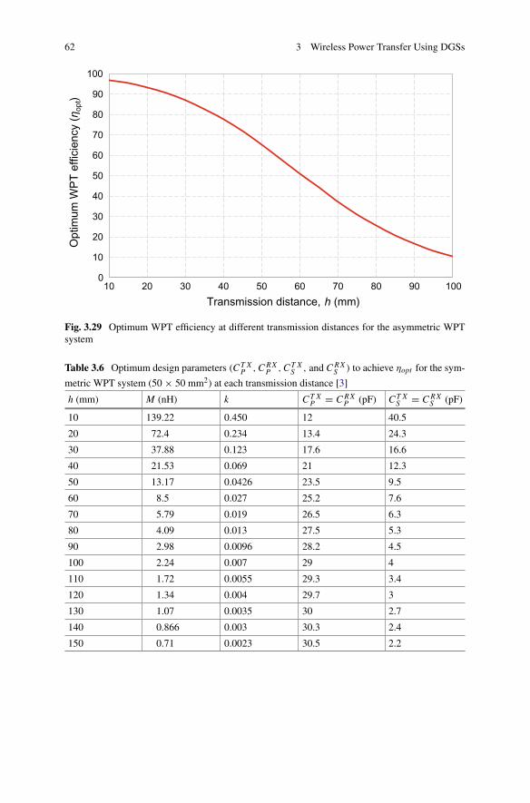
62 3 Wireless Power Transfer Using DGSs
0
10
20
30
40
50
60
70
80
90
100
10 20 30 40 50 60 70 80 90 100
Opt
imum
WPT
effi
cien
cy (η
opt)
Transmission distance, h (mm)
Fig. 3.29 Optimum WPT efficiency at different transmission distances for the asymmetric WPTsystem
Table 3.6 Optimum design parameters (CT XP ,CRX
P ,CT XS , and CRX
S ) to achieve ηopt for the sym-
metric WPT system (50 × 50 mm2) at each transmission distance [3]
h (mm) M (nH) k CT XP = CRX
P (pF) CT XS = CRX
S (pF)
10 139.22 0.450 12 40.5
20 72.4 0.234 13.4 24.3
30 37.88 0.123 17.6 16.6
40 21.53 0.069 21 12.3
50 13.17 0.0426 23.5 9.5
60 8.5 0.027 25.2 7.6
70 5.79 0.019 26.5 6.3
80 4.09 0.013 27.5 5.3
90 2.98 0.0096 28.2 4.5
100 2.24 0.007 29 4
110 1.72 0.0055 29.3 3.4
120 1.34 0.004 29.7 3
130 1.07 0.0035 30 2.7
140 0.866 0.003 30.3 2.4
150 0.71 0.0023 30.5 2.2

3.4 Design Method of the DGS-WPT Systems 63
Table 3.7 Optimum design parameters (CT XP ,CRX
P ,CT XS , andCRX
S ) to achieve ηopt for the asym-metric WPT system at each transmission distance [3]
h (mm) M (nH) k CT XP (pF) CT X
S (pF) CRXP (pF) CRX
S (pF)
10 64.77 0.30 12 28.8 44 46.7
20 30.6 0.142 16.7 18 46 27
30 15.17 0.07 21 12.4 51 18
40 8.27 0.039 24 9 55 13
50 4.89 0.023 26 7 58 10
60 3.08 0.014 27.3 5.5 60 8
70 2.06 0.009 28.3 4.5 61 6.5
80 1.43 0.007 29 3.7 62 5.4
90 1.03 0.005 29.5 3.2 63 4.5
100 0.76 0.004 30 2.7 63.7 4
Ф = 0˚ Ф = 45˚
Ф = 90˚ Ф = 135˚ Ф = 180˚
TX
RX
50 mm
50 mm
50 mm
Fig. 3.30 Magnetic field distribution of the symmetric (50 × 50 mm2) WPT system at phasesF = 0°, 45°, 90°, 135°, and 180° [3]

64 3 Wireless Power Transfer Using DGSs
Ф = 0˚ Ф = 45˚
Ф = 90˚ Ф = 135˚ Ф = 180˚
TX
RX30 mm
50 mm
40 mm
Fig. 3.31 Magnetic field distribution of the asymmetric WPT system (TX 50 × 50 mm2 & RX 30× 30 mm2) at phases F = 0°, 45°, 90°, 135°, and 180° [3]
3.5 Fabrication and Measurements
Figure 3.32 shows themeasurement setup of the fabricatedWPTsystems (symmetric,and asymmetric, respectively) using theVectorNetworkAnalyzer (AgilentN5222A).Figure 3.33a–c displays the measured and simulated S-parameters (|S11| & |S21|) forthe offered WPT systems, also for the asymmetric WPT systems [3]. As shown, thesymmetric and asymmetric WPT systems operate at 49.5 MHz, and the measuredresults are in good agreement with the simulated results. The frequency shift betweenthemeasured and the simulated |S-parameters| is due to the tolerance of the used SMDchip capacitors (CP,i and CLS,i).
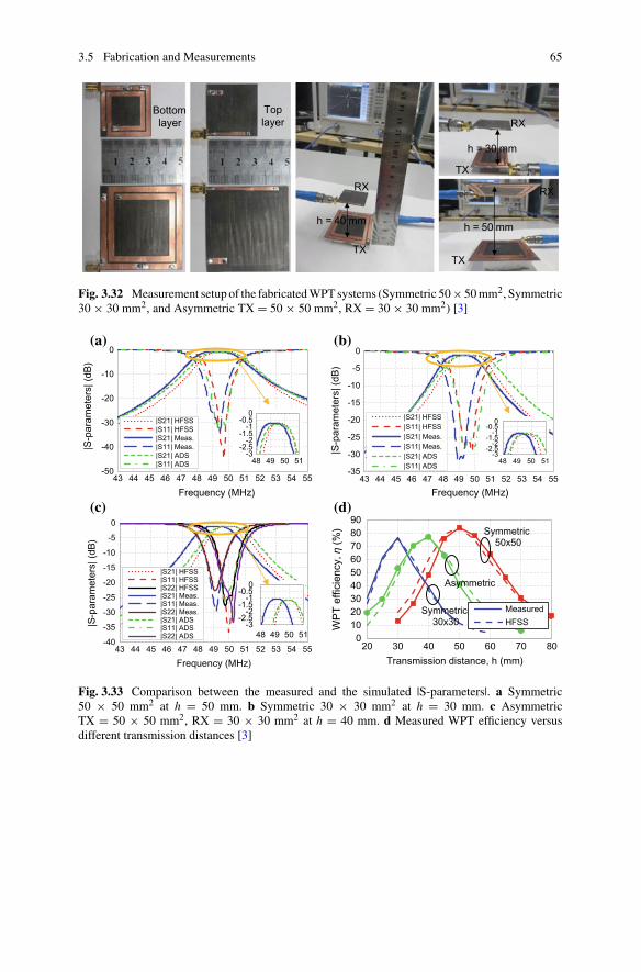
3.5 Fabrication and Measurements 65
Toplayer
Bottomlayer
TX
RX
h = 40 mm
TX
RX
h = 30 mm
TX
RX
h = 50 mm
Fig. 3.32 Measurement setup of the fabricatedWPT systems (Symmetric 50× 50mm2, Symmetric30 × 30 mm2, and Asymmetric TX = 50 × 50 mm2, RX = 30 × 30 mm2) [3]
-50
-40
-30
-20
-10
0
43 44 45 46 47 48 49 50 51 52 53 54 55
|S-p
aram
eter
s| (d
B)
Frequency (MHz)
|S21| HFSS|S11| HFSS|S21| Meas.|S11| Meas.|S21| ADS|S11| ADS
-3-2.5
-2-1.5
-1-0.5
0
-35
-30
-25
-20
-15
-10
-5
0
43 44 45 46 47 48 49 50 51 52 53 54 55
|S-p
aram
eter
s| (d
B)
Frequency (MHz)
|S21| HFSS|S11| HFSS|S21| Meas.|S11| Meas.|S21| ADS|S11| ADS
-3-2.5
-2-1.5
-1-0.5
0
-40
-35
-30
-25
-20
-15
-10
-5
0
43 44 45 46 47 48 49 50 51 52 53 54 55
|S-p
aram
eter
s| (d
B)
Frequency (MHz)
|S21| HFSS|S11| HFSS|S22| HFSS|S21| Meas.|S11| Meas.|S22| Meas.|S21| ADS|S11| ADS|S22| ADS
-3-2.5
-2-1.5
-1-0.5
0
48 49 50 51 0102030405060708090
20 30 40 50 60 70 80
WPT
effi
cien
cy, η
(%)
Transmission distance, h (mm)
MeasuredHFSS
Symmetric 50x50
Symmetric 30x30
Asymmetric
(a) (b)
(c) (d)
48 49 50 51 48 49 50 51
Fig. 3.33 Comparison between the measured and the simulated |S-parameters|. a Symmetric50 × 50 mm2 at h = 50 mm. b Symmetric 30 × 30 mm2 at h = 30 mm. c AsymmetricTX = 50 × 50 mm2, RX = 30 × 30 mm2 at h = 40 mm. d Measured WPT efficiency versusdifferent transmission distances [3]
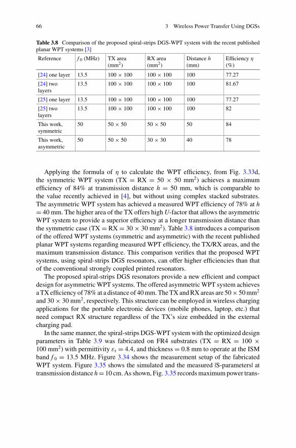
66 3 Wireless Power Transfer Using DGSs
Table 3.8 Comparison of the proposed spiral-strips DGS-WPT system with the recent publishedplanar WPT systems [3]
Reference f 0 (MHz) TX area(mm2)
RX area(mm2)
Distance h(mm)
Efficiency η
(%)
[24] one layer 13.5 100 × 100 100 × 100 100 77.27
[24] twolayers
13.5 100 × 100 100 × 100 100 81.67
[25] one layer 13.5 100 × 100 100 × 100 100 77.27
[25] twolayers
13.5 100 × 100 100 × 100 100 82
This work,symmetric
50 50 × 50 50 × 50 50 84
This work,asymmetric
50 50 × 50 30 × 30 40 78
Applying the formula of η to calculate the WPT efficiency, from Fig. 3.33d,the symmetric WPT system (TX = RX = 50 × 50 mm2) achieves a maximumefficiency of 84% at transmission distance h = 50 mm, which is comparable tothe value recently achieved in [4], but without using complex stacked substrates.The asymmetric WPT system has achieved a measured WPT efficiency of 78% at h= 40 mm. The higher area of the TX offers highU-factor that allows the asymmetricWPT system to provide a superior efficiency at a longer transmission distance thanthe symmetric case (TX = RX = 30 × 30 mm2). Table 3.8 introduces a comparisonof the offered WPT systems (symmetric and asymmetric) with the recent publishedplanar WPT systems regarding measured WPT efficiency, the TX/RX areas, and themaximum transmission distance. This comparison verifies that the proposed WPTsystems, using spiral-strips DGS resonators, can offer higher efficiencies than thatof the conventional strongly coupled printed resonators.
The proposed spiral-strips DGS resonators provide a new efficient and compactdesign for asymmetricWPT systems. The offered asymmetricWPT system achievesaTXefficiency of 78%at a distance of 40mm.TheTXandRXareas are 50× 50mm2
and 30 × 30 mm2, respectively. This structure can be employed in wireless chargingapplications for the portable electronic devices (mobile phones, laptop, etc.) thatneed compact RX structure regardless of the TX’s size embedded in the externalcharging pad.
In the samemanner, the spiral-strips DGS-WPT systemwith the optimized designparameters in Table 3.9 was fabricated on FR4 substrates (TX = RX = 100 ×100 mm2) with permittivity εr = 4.4, and thickness = 0.8 mm to operate at the ISMband f 0 = 13.5 MHz. Figure 3.34 shows the measurement setup of the fabricatedWPT system. Figure 3.35 shows the simulated and the measured |S-parameters| attransmission distance h= 10 cm.As shown, Fig. 3.35 recordsmaximumpower trans-

3.5 Fabrication and Measurements 67
Table 3.9 Optimum design parameters and equivalent RLC values of the proposed spiral-stripsDGS-WPT system (100 × 100 mm2) fabricated on FR4 substrate at f 0 = 13.5 MHz
Dimensions (mm) W f W st Lst D W t s
1.5 2.4 40 100 8 2
Equivalent circuit L (nH) R () CP (pF) Cst (pF) CLS (pF) k
550 0.15 205 7.7 42 0.04
10 cm
Fig. 3.34 Fabricated designs and measurements of the proposed spiral-strips DGS-WPT system atf 0 = 13.5 MHz [3]
fer efficiency at f 0 = 13.5 MHz with good agreement between the measured and thesimulated results. The proposedWPT system is able to provide 81.7%measured effi-ciency using one layer due to higher Q-factor (339) compared to [23, 24] (efficiency77.27%, and Q-actor = 274). In the future, we can apply the two layers (by printingauxiliary strips in the top layer to decrease the series resistance and so increase theunloaded Q-factor) that is expected to give improvement in WPT efficiency (2–3%).

68 3 Wireless Power Transfer Using DGSs
-45-40-35-30-25-20-15-10
-50
11 12 13 14 15 16
|S-p
aram
eter
s|, d
B
Frequency, MHz
Circuit sim.EM sim.Measured
-2.0-1.5-1.0-0.5
13 13.5 14
S21
S11
Fig. 3.35 Simulated and measured |S-parameters| for the proposed spiral-strips DGS-WPT systemat h = 10 cm and f 0 = 13.5 MHz [3]
3.6 Power Transmission Through the Human Body
The idea of using the electromagnetic waves as wireless power source dates backto the end of the nineteenth century when Nikola Tesla demonstrated the idea forthe transmission of electrical energy over a certain distance without any electricalconnections. Recently, due to the development of low-power-consuming electronicdevices, and the emerging the Internet of Things (IoT) technology, Wireless PowerTransfer (WPT), andEnergyHarvesting (EV) techniques have become the supportingtechnology for execution of Energy Autonomous Systems (EASs), implemented towork without onboard batteries. Although the technology of WPT is widely usednowadays for charging of portable electronic devices (mobile phones, laptops, etc.),there are other devices that can benefit from this technique such as the implantablebiomedical devices for acute diabetes and heart diseases. One of the major designchallenges of these implantable devices is the need for using small size batteries.Because of the limited batteries lifetime, it is essential to operate on patients (likethe operation of battery replacement every 2–3 years), with risks to the health andadditional costs. A feasible solution to overcome this disadvantage is the use ofwireless power transfer. WPT can be realized either by directly providing power tothe implantable device, or by charging wirelessly rechargeable batteries. Therefore,it is extremely important to focus research efforts on efficient wireless powering ofbiomedical implants.
This section tests the reliability of the symmetric (50×50mm2) spiral-stripsDGS-WPT system in Fig. 3.32 to transfer the power through a human body. Figure 3.36shows a sample representation of the existence of a human body tissue by insertionof one of the authors’ hand between the TX and the RX. Figure 3.37 displays acomparison of power transfer efficiency for the WPT system in Fig. 3.36 with andwithout insertion of the author’s hand. As shown in Fig. 3.37, there is 13% decrease
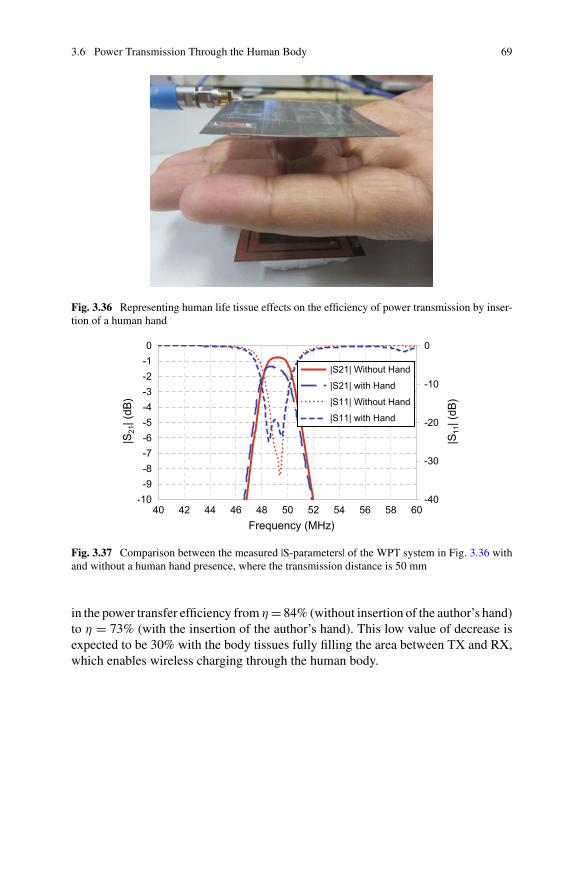
3.6 Power Transmission Through the Human Body 69
Fig. 3.36 Representing human life tissue effects on the efficiency of power transmission by inser-tion of a human hand
-40
-30
-20
-10
0
-10-9-8-7-6-5-4-3-2-10
40 42 44 46 48 50 52 54 56 58 60
|S11
| (dB
)
|S21
| (dB
)
Frequency (MHz)
|S21| Without Hand
|S21| with Hand
|S11| Without Hand
|S11| with Hand
Fig. 3.37 Comparison between the measured |S-parameters| of the WPT system in Fig. 3.36 withand without a human hand presence, where the transmission distance is 50 mm
in the power transfer efficiency from η = 84% (without insertion of the author’s hand)to η = 73% (with the insertion of the author’s hand). This low value of decrease isexpected to be 30% with the body tissues fully filling the area between TX and RX,which enables wireless charging through the human body.

70 3 Wireless Power Transfer Using DGSs
3.7 Power Handling Capability of the Proposed WPTSystems
The power handling capability can be defined as the maximum input or output powerthat a component, circuit, device, or system can provide or handle without damage.The power handling capability is limited by heating caused by conductor and dielec-tric losses. The used Rogers substrates, with a thermal conductivity of 0.5–0.7 andloss tangent of 0.001–0.0025, has been tested using the free software MWI, to calcu-late the temperature rise with RF power, and was found to be 0.18–0.25 Cº/W. TheAverage power handling capability (APHC) is calculated by (3.17) where Tmax isthe maximum operating temperature of substrate, Tamp is the ambient temperature,and T is the rate of temperature rise (C°/W). According to the formula of APHCin (3.17), our proposed structure can be used for low power applications in the rangeof 0.1–1 W. Modifications for the structure like increasing metal thickness can bemade in order to be suitable for higher power applications.
APHC = Tmax − Tamb
T(3.17)
References
1. S. Hekal, A.B. Abdel-Rahman, H. Jia, A. Allam, A. Barakat, R.K. Pokharel, A novel techniquefor compact size wireless power transfer applications using defected ground structures. IEEETrans. Microw. Theory Tech. 65(2), 591–599 (2017)
2. S. Hekal, A.B. Rahman, H. Jia, A. Allam, A. Barakat, T. Kaho, R. Pokharel, Compact wirelesspower transfer system using defected ground bandstop filters. IEEE Microw. Wirel. Compon.Lett. 26(10), 849–851 (2016)
3. S. Hekal, A.B. Abdel-Rahman, A. Allam, H. Jia, A. Barakat, R.K. Pokharel, Asymmetric wire-less power transfer systems using coupled DGS resonators. IEICE Electron. Express 13(21),20160591–20160591 (2016)
4. M. Kiani, M. Ghovanloo, An RFID-Based closed-loop wireless power transmission system forbiomedical applications. IEEE Trans. Circuits Syst. II Express Briefs 57(4), 260–264 (2010)
5. M. Zargham, P.G. Gulak, Maximum achievable efficiency in near-field coupled power-transfersystems. IEEE Trans. Biomed. Circuits Syst. 6(3), 228–245 (2012)
6. M. Zargham, P.G. Gulak, A 0.13 μmCMOS integrated wireless power receiver for biomedicalapplications, in 2013 Proceedings of the ESSCIRC (2013), pp. 137–140
7. B.M. Badr, R. Somogyi-Gsizmazia, N. Dechev, K.R. Delaney, Power transfer via magneticresonant coupling for implantable mice telemetry device, in IEEE Wirel. Power Transf. Conf.(WPTC) 2014, 259–264 (2014)
8. K. Shams, M. Ali, Wireless power transmission to a buried sensor in concrete. IEEE Sens. J.7, 1573–1577 (2007)
9. O. Jonah, S.V. Georgakopoulos, Wireless power transmission to sensors embedded in con-crete via magnetic resonance, in 2011 IEEE 12th Annual Wireless and Microwave TechnologyConference (WAMICON) (2011), pp. 1–6
10. O. Jonah, S.V. Georgakopoulos, Wireless power transfer in concrete via strongly coupledmagnetic resonance. IEEE Trans. Antennas Propag. 61(3), 1378–1384 (2013)
11. S. Jiang, S.V. Georgakopoulos, Optimum power transmission of wireless sensors embedded inconcrete, in 2010 IEEE International Conference on RFID, pp. 237–244

References 71
12. S.-M. Kim, I. Cho, J. Moon, S. Jeon, J. Choi, 5 W wireless power transmission systemwith coupled magnetic resonance, in 2013 IEEE 5th International Symposium on Microwave,Antenna, Propagation and EMC Technologies for Wireless Communications (MAPE) (2013),pp. 255–258
13. Z. Yalong, H. Xueliang, Z. Jiaming, T. Linlin, Design of wireless power supply system for theportable mobile device, in 2013 IEEE International Conference on Wireless Symposium (IWS)(2013), pp. 1–4
14. C.-J. Chen, T.-H. Chu, C.-L. Lin, Z.-C. Jou, A study of loosely coupled coils for wireless powertransfer. IEEE Trans. Circuits Syst. II Express Briefs 57(7), 536–540 (2010)
15. B.L. Cannon, J.F. Hoburg, D.D. Stancil, S.C. Goldstein, Magnetic resonant coupling as apotential means for wireless power transfer to multiple small receivers. IEEE Trans. PowerElectron. 24(7), 1819–1825 (2009)
16. A. Kurs, A. Karalis, R. Moffatt, J.D. Joannopoulos, P. Fisher, M. Soljacic, Wireless powertransfer via strongly coupled magnetic resonances. Science 317(5834), 83–86 (2007)
17. M. Kiani, M. Ghovanloo, The circuit theory behind coupled-mode magnetic resonance-basedwireless power transmission. IEEE Trans. Circuits Syst. Regul. Pap. 59(9), 2065–2074 (2012)
18. H. Hirayama, T. Amano, N. Kikuma, K. Sakakibara, An investigation on self-resonant andcapacitor-loaded helical antennas for coupled-resonant wireless power transfer. IEICE Trans.Commun. 96(10), 2431–2439 (2013)
19. X. Shi et al., Effects of coil shapes on wireless power transfer via magnetic resonance coupling.J. Electromagn. Waves Appl. 28(11), 1316–1324 (2014)
20. J. Wang et al., Study and experimental verification of a rectangular printed-circuit-board wire-less transfer system for low power devices. IEEE Trans. Magn. 48(11), 3013–3016 (2012)
21. S.Kim,B.Bae, S.Kong,D.H. Jung, J.J. Kim, J.Kim,Design, implementation andmeasurementof board-to-board wireless power transfer (WPT) for low voltage applications, in 2013 IEEE22nd Conference on Electrical Performance of Electronic Packaging and Systems (EPEPS)(2013), pp. 91–95
22. F. Jolani, Y. Yu, Z. Chen, A novel planar wireless power transfer system with strong coupledmagnetic resonances, in 2014 IEEE International Conference on Wireless Symposium (IWS)(2014), pp. 1–4
23. M.M. Falavarjani, M. Shahabadi, J. Rashed-Mohassel, Design and implementation of compactWPT system using printed spiral resonators. Electron. Lett. 50(2), 110–111 (2014)
24. F. Jolani, Y. Yu, Z. Chen, A planar magnetically coupled resonant wireless power transfersystem using printed spiral coils. IEEE Antennas Wirel. Propag. Lett. 13, 1648–1651 (2014)
25. F. Jolani, Y. Yu, Z. Chen, Enhanced planar wireless power transfer using strongly coupledmagnetic resonance. Electron. Lett. 51(2), 173–175 (2015)
26. A.B. Abdel-Rahman, A.K. Verma, A. Boutejdar, A.S. Omar, Control of bandstop response ofHi-Lo microstrip low-pass filter using slot in ground plane. IEEE Trans. Microw. Theory Tech.52(3), 1008–1013 (2004)
27. S.U. Rehman, A. Sheta, M. Alkanhal, Compact bandstop filter using defected ground structure(DGS), in2011Saudi InternationalConference onElectronics,Communications andPhotonicsConference (SIECPC) (2011), pp. 1–4
28. A. Abdel-Rahman, A. Verma, A. Boutejdar, A. Omar, Compact stub type microstrip bandpassfilter using defected ground plane. IEEEMicrow. Wirel. Compon. Lett. 14(4), 136–138 (2004)
29. A. Abdel-Rahman, A. Ali, S. Amari, A. Omar, Compact bandpass filters using defectedground structure (DGS) coupled resonators, in 2005 IEEE MTT-S International Conferenceon Microwave Symposium Digest (2005), p. 4
30. M.K. Mandal, S. Sanyal, A novel defected ground structure for planar circuits. IEEE Microw.Wirel. Compon. Lett. 16(2), 93–95 (2006)
31. S. Hekal, A.B. Abdel-Rahman, New compact design for short range wireless power transmis-sion at 1 GHz using H-slot resonators, in 2015 9th European Conference on Antennas andPropagation (EuCAP) (2015), pp. 1–5
32. S. Hekal, A.B. Abdel-Rahman, H. Jia, A. Allam, R.K. Pokharel, H. Kanaya, Strong resonantcoupling for short-range wireless power transfer applications using defected ground structures,in 2015 IEEE Wireless Power Transfer Conference (WPTC) (2015), pp. 1–4

72 3 Wireless Power Transfer Using DGSs
33. L.H. Weng, Y.-C. Guo, X.-W. Shi, X.-Q. Chen, An overview on defected ground structure.Prog. Electromagn. Res. B 7, 173–189 (2008)
34. G. Breed, An introduction to defected ground structures in microstrip circuits. High Freq.Electron. 7, 50–54 (2008)
35. D.M. Pozar, Microwave Engineering (Wiley, 2009)36. J.-S.G. Hong, M.J. Lancaster,Microstrip Filters for RF/Microwave Applications (Wiley, 2004)37. D. Ahn, J.-S. Park, C.-S. Kim, J. Kim, Y. Qian, T. Itoh, A design of the low-pass filter using the
novel microstrip defected ground structure. IEEE Trans. Microw. Theory Tech. 49(1), 86–93(2001)
38. N.C. Karmakar, S.M. Roy, I. Balbin, Quasi-static modeling of defected ground structure. IEEETrans. Microw. Theory Tech. 54(5), 2160–2168 (2006)
39. B. Easter, The equivalent circuit of some microstrip discontinuities. IEEE Trans. Microw.Theory Tech. 23(8), 655–660 (1975)
40. A.F. Thomson, A. Gopinath, Calculation of microstrip discontinuity inductances. IEEE Trans.Microw. Theory Tech. 23(8), 648–655 (1975)
41. R. Garg, I.J. Bahl, Microstrip discontinuities. Int. J. Electron. Theor. Exp. 45(1), 81–87 (1978)42. F.W. Grover, Inductance Calculations: Working Formulas and Tables (Courier Corporation,
2004)43. C.R. Paul, Inductance: Loop and Partial (Wiley, 2011)44. U.-M. Jow, M. Ghovanloo, Design and optimization of printed spiral coils for efficient tran-
scutaneous inductive power transmission. IEEE Trans. Biomed. Circuits Syst. 1(3), 193–202(2007)
45. T. Imura, Y. Hori,Maximizing air gap and efficiency ofmagnetic resonant coupling for wirelesspower transfer using equivalent circuit and neumann formula. Ind. Electron. IEEE Trans. On58(10), 4746–4752 (2011)
46. S.S. Mohan, M. del Mar Hershenson, S.P. Boyd, T.H. Lee, Simple accurate expressions forplanar spiral inductances. IEEE J. Solid-State Circuits 34(10), 1419–1424 (1999)
47. W.B. Kuhn, N.M. Ibrahim, Analysis of current crowding effects in multiturn spiral inductors.IEEE Trans. Microw. Theory Tech. 49(1), 31–38 (2001)
48. J. Lee, Y.-S. Lim, W.-J. Yang, S.-O. Lim, Wireless power transfer system adaptive to changein coil separation. IEEE Trans. Antennas Propag. 62(2), 889–897 (2014)
49. S. Raju, R. Wu, M. Chan, C.P. Yue, Modeling of mutual coupling between planar inductors inwireless power applications. IEEE Trans. Power Electron. 29(1), 481–490 (2014)

Chapter 4Design Methods
4.1 Introduction
The equivalent circuit model of the inductive feed [1, 2] and capacitive feed [3]resonant inductiveWPT systems have been analyzed to extract the S-parameters andthe input impedance. Nevertheless, this method of analysis results in complicateddesign procedures. For example, complex equations needed to be solved in orderto obtain the conditions for the perfect impedance matching and maximum powertransfer for the WPT systems presented in [1, 2, 4]. Other design methods, like theone explained in Sect. 4.2 [3], have been developed to yield concise design equationsusing impedance and admittance inverters. These design methods result in simpledesign equations that can indicate rapidly, and accurately, the perfect impedancematching conditions.
4.2 Design Method #1
A conventional wireless power transfer (WPT) system composed of two coupledresonant coils is shown in Fig. 4.1a [3]. The coils are represented by inductors, LP1
and LP2, and the parallel capacitors, CP1 and CP2, respectively. The series capacitorsCS1 and CS2 connect the transmitting coil to a power source, and the receiving coilto a load, respectively. An equivalent circuit based on admittance inverters can beused to provide concise analytic design equations to find the lumped element valuesshown in Fig. 4.1a. Figure 4.1b shows the equivalent circuit of Fig. 4.1a which iscomposed of two resonant coils. Parallel resonators are used to model the resonantcoils, as the impedance of each resonant coil is maximum at the resonant frequency[5]. Admittance inverters with inverter values of JS1 and JS2, connect the sendingand receiving coils to the source and the load, respectively. An admittance inverterwith an inverter value of Jm connects the two coils.
© Springer Nature Singapore Pte Ltd. 2019S. Hekal et al., Compact Size Wireless Power Transfer Using DefectedGround Structures, Energy Systems in Electrical Engineering,https://doi.org/10.1007/978-981-13-8047-1_4
73

74 4 Design Methods
Fig. 4.1 A wireless powertransfer systems using twocoils [3]
LP2LP1
CS2CS1
V
RRCP2CP1
M
L2L1
V
RRC2C1
JS1 Jm JS2
YS1 YS2Ym
(a)
(b)
The conditions under which the equivalences shown in Fig. 4.2 are valid can begiven by [3]:
CS1 = JS1
ω0
√1 − (JS1R)2
CS1e = CS1
1 + (ω0CS1R)2
CS2 = JS2
ω0
√1 − (JS2R)2
CS2e = CS2
1 + (ω0CS2R)2(4.1)
The ABCD matrix of the circuit in the right side of Fig. 4.2c, can be obtained, atthe operating frequency as follows:
ABCDr =[
1 01
jω0L11
][1 − 1
j Jm
+ j Jm 1
][1 01
jω0L21
]
=[
1ω0L2 Jm
− 1j Jm
j Jm + 1jω2
0L1L2 Jm1
ω0L1 Jm
]
(4.2)

4.2 Design Method #1 75
Fig. 4.2 Equivalent circuitsof admittance inverters inFig. 4.1b [3]
(a)
(b)
(c)
Similarly, the ABCDmatrix of the circuit in the left side of Fig. 4.2c can be givenby
ABCDl =[
LP1M jω0
LP1LP2−M2
M1
jω0MLP2M
]
(4.3)
The equivalency can be achieved when the two matrices ABCDr and ABCDl
are identical to each other. By equating (4.2) and (4.3), the two circuits in Fig. 4.2ccan be shown to be equivalent, when (4.4) is satisfied.
LP1 = L1
1 − ω20L1L2 J 2
m
LP2 = L2
1 − ω20L1L2 J 2
m
M = ω0L1L2 Jm1 − ω2
0L1L2 J 2m
(4.4)
With the knowledge of the design constraints for the TX and RX resonators, theequivalent circuit elements LP1, LP2, and M are calculated easily. By substitution of

76 4 Design Methods
LP1, LP2, andM in the system of equations (4.4), we can get the values of L1, L2, andJm.
Continue applying the design method by substitution in (4.5) to find C1 and C2
to achieve resonance at ω0 [3].
C1 = 1
L1ω20
,C2 = 1
L2ω20
(4.5)
The impedance matching condition needed to achieve the maximum power trans-fer from the source to the load, can be used to obtain the input and output admittanceinverters (JS1 and JS2). The input admittances looking into the input port of eachinverter at the resonant frequency can be given by
YS2 = J 2S2
1/R
= J 2S2R
Ym = J 2m
YS2= J 2
m
J 2S2R
YS1 = J 2S1
Ym= J 2
S1 J2S2R
J 2m
(4.6)
Perfect impedance matching is obtained when the input admittance seen lookinginto the input port of the first inverter, YS1, is identical to the source admittance, 1/R.Consequently, the circuit shown in Fig. 4.1b achieves the maximum power transferfrom the source to the load provided that
JS1 JS2R = Jm (4.7)
In the symmetric system, JS1 = JS2. In the asymmetric system, we assume JS1 orJS2 to get the other. By substitution of JS1 and JS2 in (4.1), we can get the values ofCS1 and CS2 that are realized in our circuit model by CS1 = Cst1 + CLS1, CS2 = Cst2
+ CLS2 [6].Finally, we calculate CP1 and CP2 using (4.8) as follows:
CP1 = C1 − CS1e,
CP2 = C2 − CS2e (4.8)
The following steps present the implementation of the design method #1 that canbe applied for the proposed DGS WPT systems as follows [6]:
1. Define the required RX size (D2 ×D2), then the necessary transmission distance(h) or the target WPT efficiency (η).
2. For the maximum WPT efficiency:

4.2 Design Method #1 77
In the symmetric systems, we need D1 = D2 = h; where D1 and D2 are theouter diameters of both the TX and RX structures, respectively, and h is thetransmission distance.
B. In the asymmetric systems, we need√GMA = h, where GMA is
the geometric mean area of the TX and RX structures, GMA =√T Xsize × RXsize. Hence, TX size should be equal to GMA2/RX size
→ D1 = h2/D2.
3. Extract the optimum design dimensions (W t,i, si, and N i) for both the TX andRX structures that achieve the highest U-factor (U = k
√Q1Q2).
4. By substitution with the design parameters defined and calculated using steps1–3 in (3.10)–(3.16), we can get the values LP1, LP2, R1, R2,M, and K.
5. Applying the analytic design method discussed above and reported in details in[3] by substitution in (4.1), (4.4), (4.5), (4.7), and (4.8), respectively.
6. Apply the equivalent circuit elements on the circuit simulator (ADS) for verifi-cation and pre-optimization of the capacitor values CP1, CP2, CS1, and CS2.
Define the design constraints:RX area = D2 x D2TX area = D1 x D1
Start
Calculate the equivalent circuit parameters LP1,R1, LP2, R2,M, and k
By using Matlab, compute the initial design parameters Wt1, Wt2, s1, s2 , N1, and N2 that give
the optimum U-factor, U =
Solve the following system of equations using matlab to get L1, L2, and Jm
Define the operating frequency to get C1,C2 using
End
Apply the impedance matching condition to get JS1and JS2
Is the WPT system
symmetric?
Assume JS1 then calculate JS2
Yes No
Solve the following system of equations to get CS1 , CS2,CP1, and CP2
,
,
,
Apply the extracted design parameters on HFSS for fine tuning and final optimization
CS1 and CS2 are realized by CS1 = Cst1 + CLS1and CS2 = Cst2 + CLS2
Fig. 4.3 Flowchart of design method #1

78 4 Design Methods
7. Finally, apply the optimum design parameters of the proposed WPT system onthe full-wave EM simulator (HFSS) for fine tuning and final optimization.
The implementation steps of design method #1 are summarized in the flowchartshown in Fig. 4.3.
4.3 Design Method #2
Wepresent a novel designmethod for coupled printed spiral resonatorsWPT systems.This design approach extends the concept of J-inverters and models the coupledresonators WPT system as a second-order Butterworth BPF. Figure 4.4a presents theproposed system block diagram. Each spiral inductor is loaded by a parallel capacitorto achieve resonance at the target resonance frequency. Also, a series capacitor isadded to both of the TX/RX pairs to improve impedance matching. The equivalentcircuit is shown in Fig. 4.4b.
Figure 4.4c details the equivalent circuit showing the J-inverters. Equations (4.9)and (4.10) calculate the equivalent circuit elements of the pi model (LM, La, andLb) representing the magnetic coupled inductors (L1 and L2). The generalized J-inverters can be computed using (4.11) [7], and g0, g1, g2 and g3 are the prototypefilter’s (Butterworth) coefficients where g0 = g3 = 1 and g1 = g2 = √
2. RS and RL
are the source and load resistances, respectively, RS = RL = R0 = 50. FBW isthe system fractional bandwidth, and b1 and b2 are the susceptance slope parameters.The ith susceptance slope parameter (bi ) can be calculated using (4.12) [7]. Where,Bi is the ith susceptance and Lri is the ith resonating inductance.
Lm = L1L2 − M2
M
La = L1L2 − M2
L2 − M
Lb = L1L2 − M2
L1 − M(4.9)
Lr1 = La//Lm → Lr1 = L1 − M2/L2
Lr2 = Lb//Lm → Lr2 = L2 − M2/L1 (4.10)
J01 = √b1FBW/R0g0g1
J12 = FBW√b1b2/g1g2
J23 = √b2FBW/R0g2g3 (4.11)
bi = (ω0/2) × ∂Bi/∂ω|ω=ω0 = 1/ω0Lri (4.12)
J12 = 1/ω0Lm (4.13)

4.3 Design Method #2 79
RX
TX
D1
D2
CP2CP1 L2L1
M
VRL
RS
CS1 CS2
Lm
CP2CP1V
RLRS
CS2CS1
LbLa
(a) (b)
Lm
Cr2Cr1
V
RLRS
CS2CS1
-Cse2-Cse1 Lr1 Lr2-Lm-Lm
J01 J12 J23(c)
Fig. 4.4 a Proposed system block diagram. b Its equivalent circuit. c Equivalent circuit based onJ-inverters
Cs1 = J01
ω0
√1 − (J01R0)
2
Cse1 = Cs1
1 + (ω0Cs1R0)2
Cs2 = J23
ω0
√1 − (J23R0)
2
Cse2 = Cs2
1 + (ω0Cs2R0)2 (4.14)
FBW = J12√g1g2/b1b2 = (1/Lm)
√g1g2Lr1Lr2 (4.15)
J01 =√
J12√g1g2
R0g0g1
√b1/b2 =
√J12
√g1g2
R0g0g1
√Lr2/Lr1

80 4 Design Methods
Specify the TX/RX sizes (DxD), the target transmission distance (h),
and the operating frequency ( )
Determine the TX/RX self-inductance ( ), the resistance ( ), and the
mutual inductance ( ) using (3.10), (3.11), and (3.15), respectively.
Substitute in (4.9)-(4.17) to calculate the values of the circuit
components ( and )
Fig. 4.5 The analytical design procedure of the symmetric WPT system
J23 =√
J12√g1g2
R0g2g3
√b2/b1 =
√J12
√g1g2
R0g2g3
√Lr1/Lr2 (4.16)
Cp1 = Cr1 − Cse1
Cr1 = 1/ω20Lr1 Lr1 = L1 − M2/L2
Cp2 = Cr2 − Cse2
Cr2 = 1/ω20Lr2Cr2 = 1/ω2
0Lr2 Lr2 = L2 − M2/L1
(4.17)
The relations between the J-inverters and the circuit component can be derivedeasily. The center J-inverter (J12) is related to the mutual coupling between the tworesonators as (4.13), where ω0 is the angular resonant frequency. Also, the inputand output J-inverters are related to the coupling capacitors as (4.14) [7]. Using(4.11) and (4.12), we derive the FBW as (4.15). Also, using (4.11) and (4.15),the input and output J-inverters reduce to (4.16). Then, the resonating capacitorscan be computed using (4.17). Finally, the design procedures for the symmetric andasymmetric structures are shown in Figs. 4.5 and 4.6.
4.4 Verification of Design Method #2
4.4.1 Symmetric WPT System
In this section, we apply the proposed method on the symmetric WPT system at50 MHz frequency. The size of the receiver is set to 30 × 30 mm2. Applying thedesign procedures shown in Fig. 4.5, the optimumWPT separation distance is h = 30mm. The design model is shown in Fig. 4.7.

4.4 Verification of Design Method #2 81
Specify the RX size ( ), the target transmission distance (h), and
the operating frequency ( )
Determine the TX and RX self-inductances ( and ), the resistances
( and ), and the mutual inductance ( ) using (3.10), (3.11), and
(3.15), respectively.
Apply and substitute in (4.9)-(4.17) calculate the values of the circuit
component ( )
Use to determine the required TX size ( )
Fig. 4.6 The analytical design procedure of the asymmetric WPT system
dh substrate
via
(a) (b)
Fig. 4.7 The proposed WPT system a 3D view. b Planar view
A two-turn spiral inductor topology is selected. The used substrate is RO3003(εr = 3, Tsub = 0.762 mm and t = 18 µm). The dimensions and the components ofthe WPT system and its performance in terms of WPT efficiency (ηWPT ) are sum-marized in Table 4.1. The spiral inductor parameters (trace width, trace separation,and number of turns) are selected to maximize the obtainable WPT efficiency [8].

82 4 Design Methods
Table 4.1 Summary of the designed, simulated and optimized parameters and performance of thesymmetric WPT system
Method Analytical Simulated (ADS) Optimized (HFSS)
f 0 (MHz) 50 49.94 50
DT Xo × DT X
o (mm2) 30 × 30 – 30 × 30
DRXo × DRX
o (mm2) 30 × 30 – 30 × 30
lT XF = l RXF (mm) – – 5
WT XF = WRX
F (mm) – – 1
gT XF = gRXF (mm) – – 2.5
h (mm) 30 – 30
N1 = N2 2 – 2
WT X = WRX (mm) 2.5 – 2.5
sT X = sRX (mm) 1 – 1
LT X = LRX (nH) 149 149 –
M (nH), k 6.76, 0.045 6.76, 0.045 –
RT X = RRX () 0.3 0.3 –
CT XP = CRX
P (pF) 54.4 54.4 54
CT XS = CRX
S (pF) 14.4 14.4 13
ηWPT (%) – 75.2 75.5
Fig. 4.8 Comparisonbetween the simulated|S-Parameters| of thesymmetric WPT systemusing ADS and HFSS
-60
-50
-40
-30
-20
-10
0
40 45 50 55 60
|S-P
aram
eter
s| (d
B)
Frequency (MHz)
HFSSADS
|S21|
|S11|
We compute the WPT efficiency (ηWPT ) of a perfectly matched system asηWPT = |S21|2. Where |S21| is the magnitude of the transmission coefficient. Theoptimized capacitors values using HFSS agree with the calculated ones, which provethe accuracy of the proposed analytical design procedure. Also, the simulated per-formance using ADS and HFSS is compared in Fig. 4.8 showing good agreement.

4.4 Verification of Design Method #2 83
4.4.2 Asymmetric WPT System
A major limitation of the symmetric resonant inductive coupling WPT system isthe transmission distance (h). The WPT separation is limited to the square root ofthe spiral inductor area to achieve the critical coupling; hence, a maximum WPTefficiency [8]. So, the size of the spiral resonator must be increased to allow for alarger transmission distance. However, increasing the size is not desirable for manyWPT applications such as medical implants. For that matter, we maintain the sizeof the receiver and increase the transmission distance by increasing the transmitter’ssize. Hence, the transmission distance should be related to the effective geometricalarea that result in the mutual coupling between the TX and the RX; hence, wecalculate the transmission distance as
h = √Aef f =
√√AT X × ARX =
√DT X
o × DRXo (4.18)
where AT X = (DT X
o
)2and ARX = (
DRXo
)2are the areas of the TX and RX, respec-
tively.According to (4.18), by applying the design process in Fig. 4.6, we increase the
transmission distance to 38 mm for a transmitter and receiver sizes of 50 × 50 mm2
and 30× 30mm2, respectively. The performance is summarized in Table 4.2. Similarto the symmetric case, the design parameters of the TX/RX spirals are selected tomaximize the obtainable efficiency [8]. Figure 4.9 shows the fabricated asymmetricWPT system and the measurement setup using VNA. The measured and simulatedperformances shown in Fig. 4.10 have a good agreement. The used capacitors valuesin the measurements are CT X
P = 54 pF, CRXP = 23 pF, CT X
S = 23 pF, and CRXS =
9 pF, which agree with the computed values in Table 4.2. The agreement betweenthe analytical model, the circuit simulations, the EM simulations, and the measuredperformance is an additional proof to the proposed design procedure.
In summary, a simple designmethod for the resonant inductive coupled symmetricand asymmetric WPT systems have been proposed. This technique models a WPTas a second-order bandpass filter (BPF). In this approach, mutual coupling betweenthe TX and RX is used to compute the values of the J-inverters. After that, we extractthe required circuit components from the J-inverters. An asymmetric WPT system isfabricated based on the proposed design method. The measured performance of thefabricated asymmetricWPT system is in good agreement with the simulated one.Weachieve a WPT efficiency of 75% within a transmission distance of 38 mm for theasymmetricWPT system. The sizes of the TX andRXof this system are 50× 50mm2
and 30 × 30 mm2, respectively. A comparison between the different design methodsthat have been presented in the chapter is shown in Table 4.3. The comparisondistinguishes between the different methods in terms of the used technique, theconsumed time, and finally the applicability for asymmetric systems.

84 4 Design Methods
Table 4.2 Summary of the designed, simulated and optimized parameters and performance of theasymmetric WPT system
Method Analytical Simulations (ADS) Optimized (HFSS)
f 0 (MHz) 50 49.94 50
DT Xo × DT X
o (mm2) 50 × 50 – 30 × 30
DRXo × DRX
o (mm2) 30 × 30 – 30 × 30
lT XF = l RXF (mm) – – 5
WT XF = WRX
F (mm) – – 1
gT XF = gRXF (mm) – – 2.5
h (mm) 38 – 38
N1 = N2 2 – 2
WT X , WRX (mm) 3, 2.5 – 3, 2.5
sT X , sRX (mm) 1, 1 – 1, 1
LT X , LRX (nH) 339, 149 339, 149 –
M (nH), k 9.6, 0.043 9.6, 0.043 –
RT X , RRX () 0.5, 0.3 0.5, 0.3 –
CT XP , CRX
P (pF) 23.5, 54.8 23.5, 54.8 23.5, 55
CT XS , CRX
S (pF) 9.6, 14 9.6, 14 9, 12.5
ηWPT (%) – 77.3% 77.4%
Bottom layers
Top layers
TX
TX RX
RX
Fig. 4.9 Measurement setup of the fabricated asymmetric WPT system

References 85
Fig. 4.10 Comparisonbetween the circuit (ADS),EM (HFSS) simulations, andthe measured performance ofthe fabricated asymmetricWPT system
-30
-25
-20
-15
-10
-5
0
45 46 47 48 49 50 51 52 53 54 55
|S-P
aram
eter
s|
Frequency (MHz)
ADSHFSSMeasured
|S11|
|S21|
-2.5
-2
-1.5
-1
49 50 51
Table 4.3 Comparison between the different design methods for resonant inductive WPT systems
Traditional method Design method #1 [3] Design method #2(proposed)
Technique Depends oniterations to find thedesign values
Models the systemusing admittance (J-)inverters then find thedesign values byachieving theimpedance matching
Models the system asa second-order BPFusing admittanceinverters then find thedesign values thatachieve the filterequation
Time consumption Very long Short Very short
Applicability forasymmetric systems
Very hard with a lotof assumptions
Simple, assumptionsare required
Very simple and noassumptions areneeded
References
1. A.P. Sample, D.T. Meyer, J.R. Smith, Analysis, experimental results, and range adaptation ofmagnetically coupled resonators for wireless power transfer. IEEE Trans. Ind. Electron. 58(2),544–554 (2011)
2. S. Cheon, Y.-H. Kim, S.-Y. Kang, M.L. Lee, J.-M. Lee, T. Zyung, Circuit-model-based analysisof awireless energy-transfer systemvia coupledmagnetic resonances. IEEETrans. Ind. Electron.58(7), 2906–2914 (2011)
3. J. Lee, Y.-S. Lim, W.-J. Yang, S.-O. Lim, Wireless power transfer system adaptive to change incoil separation. IEEE Trans. Antennas Propag. 62(2), 889–897 (2014)
4. L. Chen, S. Liu, Y.C. Zhou, T.J. Cui, An optimizable circuit structure for high-efficiencywirelesspower transfer. IEEE Trans. Ind. Electron. 60(1), 339–349 (2013)
5. D.M. Pozar, Microwave Engineering (Wiley 2009)6. S. Hekal, Adel B. Abdel-Rahman, A. Allam, H. Jia, A. Barakat, R.K. Pokharel, Asymmetric
wireless power transfer systems using coupled DGS resonators. IEICE Electron. Exp. 13(21),20160591 (2016)

86 4 Design Methods
7. G.L.Matthaei, L. Young, E.M.T. Jones,Microwave Filters, Impedance-Matching Networks, andCoupling Structure (Artech House, 1980)
8. U.-M. Jow, M. Ghovanloo, Design and optimization of printed spiral coils for efficient tran-scutaneous inductive power transmission. IEEE Trans. Biomed. Circuits Syst. 1(3), 193–202(2007)

Chapter 5Future Directions
5.1 Summary
The world nowadays is dominated by portable electronic devices. Furthermore,researchers and industrial organizations are energetically exploring new portabledevices, particularly devices that combine more functions, and devices (sensors) thatmonitor the world around us, such as the Internet of Things (IoT) technology.
The essential demand for all electronic devices is the source of electrical power.With the ubiquity of portable electronic devices with low power needs, the powerdemands of each device through charging cables are becoming inevitable. However,the huge number of portable devices increases the number of charging wires leadingto greater complexity, user inconvenience, increased costs, and decreased systemsustainability.
This book aims to resolve this issue by proposing new efficient and low-profiledesign for short-rangeWPT systems using quasi-lumped elements based on defectedground structures (DGS). Chapter 2 discussed the different techniques of WPT (nearfield and far field) usingbulky lumpedelements andprinted resonators, thenpresentedthe theory behind using the defected ground structures (DGS) for low-profile band-pass Filters (BPF), and band-stop filters (BSF). DGSs exhibit BPF characteristics byintroducing a discontinuity in the feeding microstrip line above the DGS’s slots andadding stubs for matching [1]. In the same manner, band-pass characteristics appearwhen two DGS resonators are coupled back to back, and power can be transferredfrom source to load through the DGS resonators [1].
As outlined in Chap. 3, different shapes of DGSs like (H, semi H, and spiralstrips) have been analyzed and fabricated to design highly efficient and low-profileDGS-WPT systems. In the proposed DGS-WPT system, electrical coupling is usedfor feeding. Thus, the limitations of the feeding loop, used in inductive feeding, areavoided, and a higher achievable unloaded Q-factor is possible with compact sizesand higher power transfer efficiency [1]. The circuit model of the proposed WPTsystem is derived by extracting the equivalent circuit parameters (RLC) using quasi-
© Springer Nature Singapore Pte Ltd. 2019S. Hekal et al., Compact Size Wireless Power Transfer Using DefectedGround Structures, Energy Systems in Electrical Engineering,https://doi.org/10.1007/978-981-13-8047-1_5
87
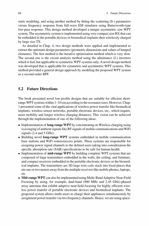
88 5 Future Directions
static modeling, and using another method by fitting the scattering (S-) parametersversus frequency response from full-wave EM simulator using Butterworth-typelow-pass response. This design method developed a unique asymmetric size WPTsystem. The asymmetric system is implemented using very compact size RX that canbe embedded in the portable devices or biomedical implants then wirelessly chargedby large size TX.
As detailed in Chap. 4, two design methods were applied and implemented toextract the optimum design parameters (geometric dimensions and values of lumpedelements). The first method is the iterative optimization method which is very slow.The second one is the circuit analysis method using the admittance (J-) inverterswhich is fast, but applicable to symmetricWPT systems only. A novel designmethodwas developed that is applicable for symmetric and asymmetric WPT systems. Thismethod provided a general design approach by modeling the proposed WPT systemas a second-order BPF.
5.2 Future Directions
The book presented novel low-profile designs that are suitable for efficient short-rangeWPT systemswithin 1–10 cm according to the resonator sizes. However, Chap.1 presented some of the vital applications of wireless power transfer like biomedicalimplants, wireless sensor networks, portable electronic devices, etc., which require,more mobility and longer wireless charging distances. This vision can be achievedthrough the implementation of one of the following ideas:
• Implementation of long-rangeWPT by concentrating onWireless charging usingscavenging of ambient signals like RF signals ofmobile communications andWiFisignals (2.4 and 5 GHz).
• Building novel long-range WPT systems embedded in mobile communicationbase stations and WiFi routers/access points. These systems are responsible forassigning power signal channels to the defined users taking into consideration thespecific absorption rate (SAR) specifications to be safe for human health.
• Implementation of mid-range WPT by building complete WPT systems that arecomposed of large transmitters embedded in the walls, the ceiling, and furniture,and compact receivers embedded in the portable electronic devices or the biomed-ical implants. The transmitters are 3D large wire coils stuck into fixed places thatare one or twometers away from themultiple receivers likemobile phones, laptops,etc.
• Mid-rangeWPT can also be implemented usingMulti-BandAdaptive Near-FieldFocusing by using, for example, dual-band (900 MHz and 2.45 GHz)-phasedarray antennas that exhibit adaptive near-field focusing for highly efficient wire-less power transfer of portable electronic devices and biomedical implants. Theproposed system allows multi-users to charge their appliances simultaneously byassignment power transfer via two frequency channels. Hence, we are using space-

5.2 Future Directions 89
User 1
User 2
User 3
Beacon signal
Beacon signal
Beacon signal
Smart antennas system
User 4
Beacon signal
Fig. 5.1 The proposed WPT system using dual-band adaptive near-field focusing
Fig. 5.2 The difference in the received RF power density between the implementation of near-fieldfocusing and far-field focusing using 8 × 8 array of single-band antennas [6]
divisionmultiple access (SDMA) and frequency-divisionmultiple access (FDMA)at the same time, as shown in Fig. 5.1. The proposed WPT system can be installedin the ceiling of homes, restaurants, supermarkets, etc.
By employing NFF, more power will be transmitted before the effective isotropicradiated power (EIRP) limit is reached due to the inherent far-field diffusing [2–5].As discussed in [2–5], and the studies performed in [6], we can get a narrower beamand an increase of 48% in the received power density to the target as shown in Fig. 5.2.

90 5 Future Directions
W0
W1
WM-1
+.....
Array Antenna
Weights of phase shifters
θ1DOA Estimation Beamformer
θ1
Single band adaptive near-field focusing
MUSIC algorithm MMSE Technique
Power signal
The proposed Dual band adaptive near-field focusing
W0
W1
WM-1
+.....Array of Dual band
Antenna Elements
Weights of phase shifters
θ1 θ2DOA Estimation Beamformer
θ1
θ2
W0
W1
WM-1
+
Weights of phase shifters
F1
F2
∑∑
∑
MUSIC algorithm MMSE Technique
θ1 θ2
Power signal
Power signalIncident beacon signals
Directed power signals
(a)
(b)
Fig. 5.3 Implementation of adaptive near-field focusing for a Single band. b Dual band
Thanks to the usage of dual-band antennas as array elements, we expect thefollowing results:
1. Multi-user WPT system.2. High WPT efficiency (one user can receive more power via two channels).
The schematic diagram of the proposed system is shown in Fig. 5.3b. Once thebattery level decreases, themobilewill send a beacon signal to request power channel.The direction of arrival (DOA) and localization of targets is performed usingMUSICalgorithm. The system will assign power channel slots (F1, F2, or both). The DSPplatformwill focus power at the targets usingMMSE beamforming technique. Everytwo minutes, DOA estimation will be performed to locate the mobile handsets.

References 91
References
1. S. Hekal, Adel B. Abdel-Rahman, A. Allam, H. Jia, A. Barakat, R.K. Pokharel, Asymmetricwireless power transfer systems using coupledDGS resonators. IEICEElectron. Express 13(21),20160591 (2016)
2. M. Bogosanovic, A.G. Williamson, Microstrip antenna array with a beam focused in the near-field zone for application in noncontact microwave industrial inspection. IEEE Trans. Instrum.Meas. 56(6), 2186–2195 (2007)
3. Y.D. Huang, M. Barkat, Near-field multiple source localization by passive sensor array. IEEETrans. Antennas Propag. 39, 968–975 (1991)
4. A. Buffi, P. Nepa, G.Manara, Design criteria for near-field focused planar arrays. IEEEAntennasPropag. Mag. 54(1), 40–50 (2012)
5. R. Van der Linden, H.J. Visser, Analysis, design and realization of a near-field focused RF powertransfer system. J. Phys. Conf. Ser. 476(1), 012118 (2013). IOP Publishing
6. B.A. Mouris, T.A. Ali, I.A. Eshrah, A. Badawi, Adaptive near-field focusing for wireless powertransfer applications. Master Thesis, Cairo University, Egypt (2016)