Embed Size (px)
Citation preview
1244 Journal of Power Electronics, Vol. 17, No. 5, pp. 1244-1255, September 2017
https://doi.org/10.6113/JPE.2017.17.5.1244
ISSN(Print): 1598-2092 / ISSN(Online): 2093-4718
JPE 17-5-12
Performance Evaluation of Various Bus Clamped Space Vector Pulse Width Modulation Techniques
Meenu D. Nair†, Jayanta Biswas**, G. Vivek*, and Mukti Barai*
†,*Department of Electrical Engineering, National institute of Technology, Calicut, Kerala, India **Freelance Researcher
Abstract
The space vector pulse width modulation (SVPWM) technique is a popular PWM method for medium voltage drive applications. Conventional SVPWM (CSVPWM) and bus clamped SVPWM (BCSVPWM) are the most common SVPWM techniques. This paper evaluates the performance of various advanced BCSVPWM strategies in terms of their harmonic distortion and switching loss based on a uniform frame work. A uniform frame work, pulse number captures the performance parameter variations of different SVPWM strategies for various number of samples with heterogeneous pulse numbers. This work compares different advanced BCSVPWM techniques based on the modulation index and location of the clamping position (zero vector changing angle ) of a phase in a line cycle. The frame work provides a fixed fundamental frequency of 50Hz. The different BCSVPWM switching strategies are implemented and compared experimentally on a 415V, 2.2kW, 50Hz, 3-phase induction motor drive which is fed from an IGBT based 2 KVA voltage source inverter (VSI) with a DC bus voltage of 400 V. A low cost PIC microcontroller (PIC18F452) is used as the controller platform. Key words: Bus clamped PWM, Harmonic distortion, Pulse width modulation (PWM), Space vector, Voltage source inverter (VSI)
I. INTRODUCTION
Modulation techniques are used to produce inverter output voltages and currents with higher qualities for different types of loads [1]. Several modulation techniques have been proposed to meet the above mentioned objectives by achieving a wide linear modulation range, minimum switching loss and improved overall inverter efficiency. SVPWM is a popular PWM method for lower switching frequencies. It simultaneously achieves a higher DC bus utilization, lower harmonic distortion and lower switching loss. Different SVPWM switching sequences have been reported in the literature [2]-[11] for realizing the reference vector using the SVPWM technique.
Flexibility in the placement of the zero space-vector results in either the continuous or discontinuous SVPWM. Bus clamping techniques are discontinuous space vector strategies to reduce the switching losses and current
harmonics. The bus clamping techniques clamp every phase to either the positive or negative DC rail for a 1200 duration in a line cycle. The choice of the clamped leg and the duration of the clamping depend on the orientation of the desired reference voltage [3]. In BCSVPWM, 600 and 300 are the best known clamping methods. The BCSVPWM gives better spectral performance when compared to the CSVPWM in a higher modulation index. The BCSVPWM techniques can significantly reduce the switching loss by clamping a phase to either the positive or negative DC rail. Theoretically, the switching loss can be reduced by half by clamping the phase which is carrying the highest current when compared to the CSVPWM. By utilizing the freedom of the zero state division, various bus clamping SVPWM methods can be generated. The various types of BCSVPWM methods are: (i) Basic Bus Clamping Strategy I (BBCS-I) [3]; (ii) Basic Bus Clamping Strategy II (BBCS-II) [15]; (iii) Asymmetric Zero-Changing Strategy (AZCS) [3]; (iv) Boundary Sampling Strategy-I (BSS-I) [3]; and (v) Boundary Sampling Strategy-II (BSS-II) [15]. The clamping location and duration may be changed by changing the zero vector changing angle gamma (γ) [15]-[17]. Based on the location of γ, the bus clamping techniques are further
Manuscript received Nov. 15, 2016; accepted May 21, 2017 Recommended for publication by Associate Editor Yun Zhang.
†Corresponding Author: [email protected] Tel: +91-9496178967, Fax: +91-0495-2287250, Nat’l Inst. of Tech.
*Department of Electrical Engineering, National Institute of Technology, India
© 2017 KIPE
Performance Evaluation of Various Bus Clamped Space Vector Pulse Width … 1245
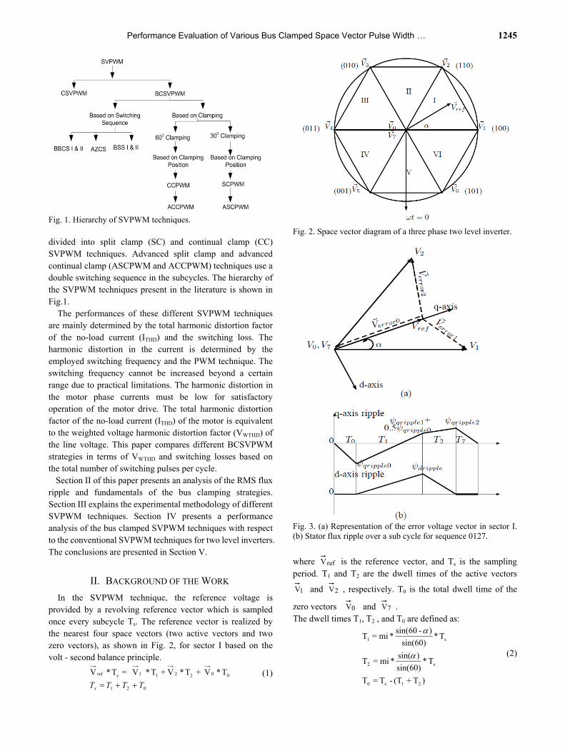
Fig. 1. Hierarchy of SVPWM techniques. divided into split clamp (SC) and continual clamp (CC) SVPWM techniques. Advanced split clamp and advanced continual clamp (ASCPWM and ACCPWM) techniques use a double switching sequence in the subcycles. The hierarchy of the SVPWM techniques present in the literature is shown in Fig.1.
The performances of these different SVPWM techniques are mainly determined by the total harmonic distortion factor of the no-load current (ITHD) and the switching loss. The harmonic distortion in the current is determined by the employed switching frequency and the PWM technique. The switching frequency cannot be increased beyond a certain range due to practical limitations. The harmonic distortion in the motor phase currents must be low for satisfactory operation of the motor drive. The total harmonic distortion factor of the no-load current (ITHD) of the motor is equivalent to the weighted voltage harmonic distortion factor (VWTHD) of the line voltage. This paper compares different BCSVPWM strategies in terms of VWTHD and switching losses based on the total number of switching pulses per cycle. Section II of this paper presents an analysis of the RMS flux ripple and fundamentals of the bus clamping strategies. Section III explains the experimental methodology of different SVPWM techniques. Section IV presents a performance analysis of the bus clamped SVPWM techniques with respect to the conventional SVPWM techniques for two level inverters. The conclusions are presented in Section V.
II. BACKGROUND OF THE WORK
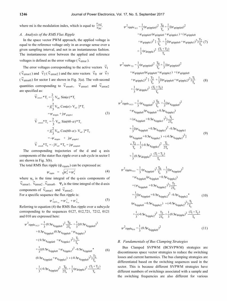
In the SVPWM technique, the reference voltage is provided by a revolving reference vector which is sampled once every subcycle Ts. The reference vector is realized by the nearest four space vectors (two active vectors and two zero vectors), as shown in Fig. 2, for sector I based on the volt - second balance principle.
021
002211sref T * V +T * V +T * V =T *V
TTTTs (1)
Fig. 2. Space vector diagram of a three phase two level inverter.
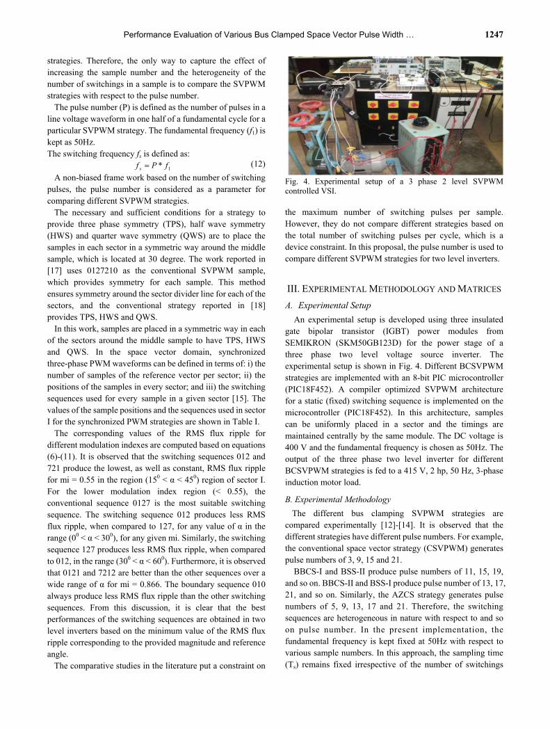
Fig. 3. (a) Representation of the error voltage vector in sector I. (b) Stator flux ripple over a sub cycle for sequence 0127.
where refV is the reference vector, and Ts is the sampling period. T1 and T2 are the dwell times of the active vectors
V1and V2 , respectively. T0 is the total dwell time of the
zero vectors 0V and V7 . The dwell times T1, T2 , and T0 are defined as:
)T+(T -T =T
T* sin(60)
)sin(*mi=T
T* sin(60)
)-sin(60*mi=T
21s0
s2
s1
(2)
1246 Journal of Power Electronics, Vol. 17, No. 5, September 2017
where mi is the modulation index, which is equal to .
A. Analysis of the RMS Flux Ripple
In the space vector PWM approach, the applied voltage is equal to the reference voltage only in an average sense over a given sampling interval, and not in an instantaneous fashion. The instantaneous error between the applied and reference
voltages is defined as the error voltage ( errorV ).
The error voltages corresponding to the active vectors 1V
( error1V ) and 2V ( error2V ) and the zero vectors 0V or 7V
( error0V ) for sector I are shown in Fig. 3(a). The volt-second
quantities corresponding to error0V , error1V and error2V are specified as:
qripple00ref0error0
qripple2dripple
2ref DC
2DC2error2
qripple1dripple
1ref DC
1DC1error1
j =T*jV- =T* V
j + - =
T*] V-)-Cos(60V 3
2j[+
T*)-Sin(60 V 3
2 =T* V
j+ =
T*] V-)Cos(V 3
2j[+
T*)Sin( V 3
2 =T*V
(3)
The corresponding trajectories of the d and q axis components of the stator flux ripple over a sub cycle in sector I are shown in Fig. 3(b). The total RMS flux ripple ( ) can be expressed as:
2q
2dripple = (4)
where ψq is the time integral of the q-axis components of
error1V , error2V , error0V . Ψd is the time integral of the d-axis
components of error1V and error2V . For a specific sequence the flux ripple is:
222
seqseqseq dqripple (5)
Referring to equation (4) the RMS flux ripple over a subcycle corresponding to the sequences 0127, 012,721, 7212, 0121 and 010 are expressed here:
T
)T+(T )(
3
1+
2T
T )(-0.5
3
1+
T
T])(-0.5 )+(0.5
*0.5-)+[(0.53
1+
T
T ]) + 0.5 (+
)+(0.5 0.5+
)[(0.53
1+
2T
T) (0.5
3
1 =
s
212dripple
s
02ripple0q
s
22ripple0qripple1qripple0q
ripple0q2
ripple1qripple0q
s
12ripple1qripple0q
ripple1qripple0qripple0q
2ripple0q
s
02ripple0qripple
20127
(6)
T
)T+(T )(
3
1
T
T])+ [(
3
1+
T
T ] )+
(+ ) +( +
)[( 3
1+
T
T )(
3
1 =
s
212dripple
s
22qripple1qripple0
s
12qripple1
qripple0qripple1qripple0qripple0
2qripple0
s
0 2qripple0ripple
2012
(7)
T
)T+(T )(
3
1+
T
T])+[(
3
1+
T
T ] )+
(+ ) +( +
)[( 3
1+
T
T )(
3
1 =
s
212dripple
s
12qripple2qripple0
s
22qripple2
qripple0qripple2qripple0qripple0
2qripple0
s
0 2qripple0ripple
2721
(8)
T
)T+(T )(0.5
3
1+
2T
T )(-0.5
3
1+
T
T*
])(-0.5 ) 0.5+(
0.5-)0.5+[(3
1+
2T
T ]) 0.5+ (+
)0.5( +
)[(3
1+
T
T)(
3
1 =
s
212dripple
s
12ripple1q
s
2
2ripple1qripple1qripple0q
ripple1q2
ripple1qripple0q
s
12ripple1qripple0q
ripple1qripple0qripple0q
2ripple0q
s
02ripple0q ripple
20121
(9)
T
)T+(T )(0.5
3
1+
2T
T )(-0.5
3
1+
T
T])(-0.5 ) 0.5+(
*0.5- )0.5+[(3
1+
2T
T ]) 0.5+ (+
)0.5+( +
)[(3
1+
T
T) (
3
1 =
s
212dripple
s
22ripple2q
s
12ripple2qripple2qripple0q
ripple2q2
ripple2qripple0q
s
22ripple2qripple0q
ripple2qripple0qripple0q
2ripple0q
s
02ripple0qripple
27212
(10)
2ripple0qripple
2 ) (0.5 3
1 =010 (11)
B. Fundamentals of Bus Clamping Strategies
Bus Clamped SVPWM (BCSVPWM) strategies are discontinuous space vector strategies to reduce the switching losses and current harmonics. The bus clamping strategies are differentiated based on the switching sequences used in the sector. This is because different SVPWM strategies have different numbers of switchings associated with a sample and the switching frequencies are also different for various
Performance Evaluation of Various Bus Clamped Space Vector Pulse Width … 1247
strategies. Therefore, the only way to capture the effect of increasing the sample number and the heterogeneity of the number of switchings in a sample is to compare the SVPWM strategies with respect to the pulse number. The pulse number (P) is defined as the number of pulses in a line voltage waveform in one half of a fundamental cycle for a particular SVPWM strategy. The fundamental frequency (f1) is kept as 50Hz. The switching frequency fs is defined as:
1* fPf s (12)
A non-biased frame work based on the number of switching pulses, the pulse number is considered as a parameter for comparing different SVPWM strategies. The necessary and sufficient conditions for a strategy to provide three phase symmetry (TPS), half wave symmetry (HWS) and quarter wave symmetry (QWS) are to place the samples in each sector in a symmetric way around the middle sample, which is located at 30 degree. The work reported in [17] uses 0127210 as the conventional SVPWM sample, which provides symmetry for each sample. This method ensures symmetry around the sector divider line for each of the sectors, and the conventional strategy reported in [18] provides TPS, HWS and QWS. In this work, samples are placed in a symmetric way in each of the sectors around the middle sample to have TPS, HWS and QWS. In the space vector domain, synchronized three-phase PWM waveforms can be defined in terms of: i) the number of samples of the reference vector per sector; ii) the positions of the samples in every sector; and iii) the switching sequences used for every sample in a given sector [15]. The values of the sample positions and the sequences used in sector I for the synchronized PWM strategies are shown in Table I. The corresponding values of the RMS flux ripple for different modulation indexes are computed based on equations (6)-(11). It is observed that the switching sequences 012 and 721 produce the lowest, as well as constant, RMS flux ripple for mi = 0.55 in the region (150 < α < 450) region of sector I. For the lower modulation index region (< 0.55), the conventional sequence 0127 is the most suitable switching sequence. The switching sequence 012 produces less RMS flux ripple, when compared to 127, for any value of α in the range (00 < α < 300), for any given mi. Similarly, the switching sequence 127 produces less RMS flux ripple, when compared to 012, in the range (300 < α < 600). Furthermore, it is observed that 0121 and 7212 are better than the other sequences over a wide range of α for mi = 0.866. The boundary sequence 010 always produce less RMS flux ripple than the other switching sequences. From this discussion, it is clear that the best performances of the switching sequences are obtained in two level inverters based on the minimum value of the RMS flux ripple corresponding to the provided magnitude and reference angle.
The comparative studies in the literature put a constraint on
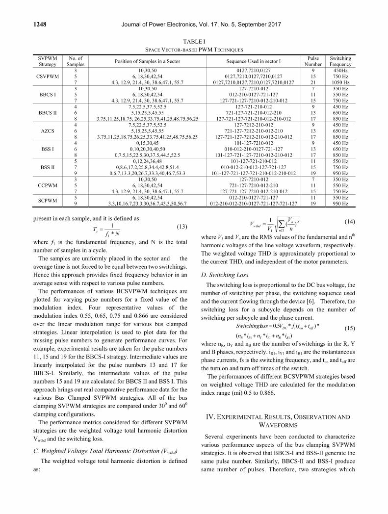
Fig. 4. Experimental setup of a 3 phase 2 level SVPWM controlled VSI. the maximum number of switching pulses per sample. However, they do not compare different strategies based on the total number of switching pulses per cycle, which is a device constraint. In this proposal, the pulse number is used to compare different SVPWM strategies for two level inverters.
III. EXPERIMENTAL METHODOLOGY AND MATRICES
A. Experimental Setup
An experimental setup is developed using three insulated gate bipolar transistor (IGBT) power modules from SEMIKRON (SKM50GB123D) for the power stage of a three phase two level voltage source inverter. The experimental setup is shown in Fig. 4. Different BCSVPWM strategies are implemented with an 8-bit PIC microcontroller (PIC18F452). A compiler optimized SVPWM architecture for a static (fixed) switching sequence is implemented on the microcontroller (PIC18F452). In this architecture, samples can be uniformly placed in a sector and the timings are maintained centrally by the same module. The DC voltage is 400 V and the fundamental frequency is chosen as 50Hz. The output of the three phase two level inverter for different BCSVPWM strategies is fed to a 415 V, 2 hp, 50 Hz, 3-phase induction motor load.
B. Experimental Methodology
The different bus clamping SVPWM strategies are compared experimentally [12]-[14]. It is observed that the different strategies have different pulse numbers. For example, the conventional space vector strategy (CSVPWM) generates pulse numbers of 3, 9, 15 and 21.
BBCS-I and BSS-II produce pulse numbers of 11, 15, 19, and so on. BBCS-II and BSS-I produce pulse number of 13, 17, 21, and so on. Similarly, the AZCS strategy generates pulse numbers of 5, 9, 13, 17 and 21. Therefore, the switching sequences are heterogeneous in nature with respect to and so on pulse number. In the present implementation, the fundamental frequency is kept fixed at 50Hz with respect to various sample numbers. In this approach, the sampling time (Ts) remains fixed irrespective of the number of switchings
1248 Journal of Power Electronics, Vol. 17, No. 5, September 2017
TABLE I SPACE VECTOR-BASED PWM TECHNIQUES
SVPWM Strategy
No. of Samples
Position of Samples in a Sector Sequence Used in sector I Pulse
NumberSwitching Frequency
CSVPWM 3 5 7
10,30,50 6, 18,30,42,54
4.3, 12.9, 21.4, 30, 38.6,47.1, 55.7
0127,7210,0127 0127,7210,0127,7210,0127
0127,7210,0127,7210,0127,7210,0127
9 15 21
450Hz 750 Hz 1050 Hz
BBCS I 3 5 7
10,30,50 6, 18,30,42,54
4.3, 12.9, 21.4, 30, 38.6,47.1, 55.7
127-7210-012 012-210-0127-721-127
127-721-127-7210-012-210-012
7 11 15
350 Hz 550 Hz 750 Hz
BBCS II 4 6 8
7.5,22.5,37.5,52.5 5,15,25,5,45,55
3.75,11.25,18.75, 26.25,33.75,41.25,48.75,56.25
127-721-210-012 721-127-721-210-012-210
127-721-127-721-210-012-210-012
9 13 17
450 Hz 650 Hz 850 Hz
AZCS 4 6 8
7.5,22.5,37.5,52.5 5,15,25,5,45,55
3.75,11.25,18.75,26.25,33.75,41.25,48.75,56.25
127-7212-210-012 721-127-7212-210-012-210
127-721-127-7212-210-012-210-012
9 13 17
450 Hz 650 Hz 850 Hz
BSS I 4 6 8
0,15,30,45 0,10,20,30,40,50
0,7.5,15,22.5,30,37.5,44.5,52.5
101-127-7210-012 010-012-210-0127-721-127
101-127-721-127-7210-012-210-012
9 13 17
450 Hz 650 Hz 850 Hz
BSS II 5 7 9
0,12,24,36,48 0,8.6,17.2,25.8,34.4,42.8,51.4
0,6.7,13.3,20,26.7,33.3,40,46.7,53.3
101-127-721-210-012 010-012-210-012-127-721-127
101-127-721-127-721-210-012-210-012
11 15 19
550 Hz 750 Hz 950 Hz
CCPWM 3 5 7
10,30,50 6, 18,30,42,54
4.3, 12.9, 21.4, 30, 38.6,47.1, 55.7
127-7210-012 721-127-7210-012-210
127-721-127-7210-012-210-012
7 11 15
350 Hz 550 Hz 750 Hz
SCPWM 5 9
6, 18,30,42,54 3.3,10,16.7,23.3,30,36.7,43.3,50,56.7
012-210-0127-721-127 012-210-012-210-0127-721-127-721-127
11 19
550 Hz 950 Hz
present in each sample, and it is defined as:
Nf
Ts *
1
1
(13)
where f1 is the fundamental frequency, and N is the total number of samples in a cycle.
The samples are uniformly placed in the sector and the average time is not forced to be equal between two switchings. Hence this approach provides fixed frequency behavior in an average sense with respect to various pulse numbers. The performances of various BCSVPWM techniques are plotted for varying pulse numbers for a fixed value of the modulation index. Four representative values of the modulation index 0.55, 0.65, 0.75 and 0.866 are considered over the linear modulation range for various bus clamped strategies. Linear interpolation is used to plot data for the missing pulse numbers to generate performance curves. For example, experimental results are taken for the pulse numbers 11, 15 and 19 for the BBCS-I strategy. Intermediate values are linearly interpolated for the pulse numbers 13 and 17 for BBCS-I. Similarly, the intermediate values of the pulse numbers 15 and 19 are calculated for BBCS II and BSS I. This approach brings out real comparative performance data for the various Bus Clamped SVPWM strategies. All of the bus clamping SVPWM strategies are compared under 300 and 600
clamping configurations. The performance metrics considered for different SVPWM strategies are the weighted voltage total harmonic distortion Vwthd and the switching loss.
C. Weighted Voltage Total Harmonic Distortion (Vwthd)
The weighted voltage total harmonic distortion is defined as:
1
2
1
)(1
n
nwthd n
V
VV (14)
where V1 and Vn are the RMS values of the fundamental and nth harmonic voltages of the line voltage waveform, respectively. The weighted voltage THD is approximately proportional to the current THD, and independent of the motor parameters.
D. Switching Loss
The switching loss is proportional to the DC bus voltage, the number of switching per phase, the switching sequence used and the current flowing through the device [6]. Therefore, the switching loss for a subcycle depends on the number of switching per subcycle and the phase current.
)***(
*)(*5.0
111 BBYYRR
offonsDC
ininin
ttfVossSwitchingL
(15)
where nR, nY and nB are the number of switchings in the R, Y and B phases, respectively. iR1, iY1 and iB1 are the instantaneous phase currents, fs is the switching frequency, and ton and toff are the turn on and turn off times of the switch.
The performances of different BCSVPWM strategies based on weighted voltage THD are calculated for the modulation index range (mi) 0.5 to 0.866.
IV. EXPERIMENTAL RESULTS, OBSERVATION AND
WAVEFORMS
Several experiments have been conducted to characterize various performance aspects of the bus clamping SVPWM strategies. It is observed that BBCS-I and BSS-II generate the same pulse number. Similarly, BBCS-II and BSS-I produce same number of pulses. Therefore, two strategies which
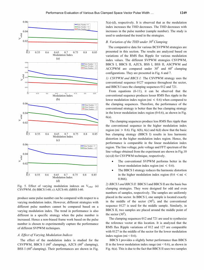
Performance Evaluation of Various Bus Clamped Space Vector Pulse Width … 1249
(a)
(b)
(c)
(d)
Fig. 5. Effect of varying modulation indexes on Vwthd. (a) CSVPWM. (b) BBCS I-60; c) AZCS-60; d)BSS I-60. produce same pulse number can be compared with respect to a varying modulation index. However, different strategies with different pulse numbers cannot be compared based on a varying modulation index. The trend in performance is also different in a specific strategy when the pulse number is increased. Hence a non-biased frame work based on the pulse number is chosen to experimentally capture the performance of different SVPWM techniques.
A. Effect of Varying Modulation Indices
The effect of the modulation index is studied for the CSVPWM, BBCS I (600 clamping), AZCS (600 clamping), BSS I (600 clamping). Their performances are shown in Fig.
5(a)-(d), respectively. It is observed that as the modulation index increases the THD decreases. The THD decreases with increases in the pulse number (sample number). The study is used to understand the trend in the strategies.
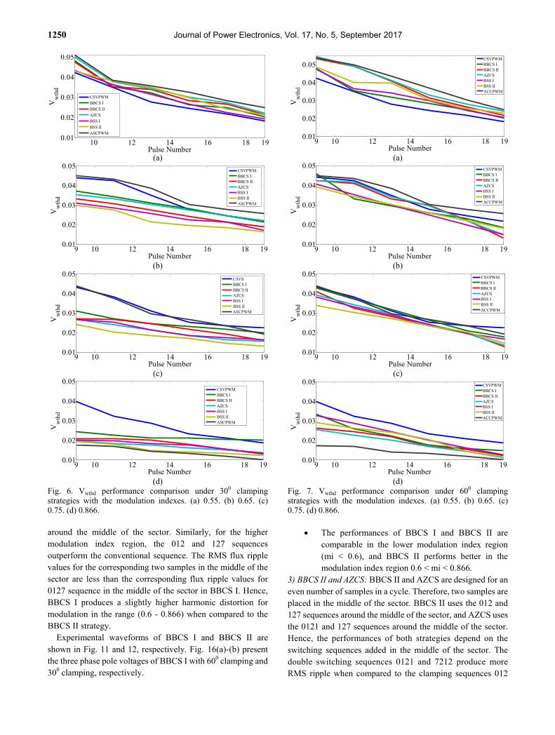
B. Variation of the THD under 300 Clamping
The comparative data for various BCSVPWM strategies are presented in this section. The results are analyzed based on variations of the RMS flux Ripple for various modulation index values. The different SVPWM strategies CSVPWM, BBCS I, BBCS II, AZCS, BSS I, BSS II, ASCPWM and ACCPWM are compared under 300 and 600 clamping configurations. They are presented in Fig. 6 and 7.
1) CSVPWM and BBCS I: The CSVPWM strategy uses the conventional sequence 0127 sequence throughout the sector, and BBCS I uses the clamping sequences 012 and 721.
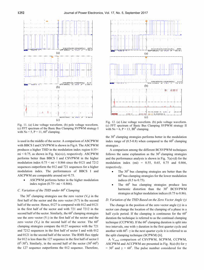
From equations (6-11), it can be observed that the conventional sequence produces lesser RMS flux ripple in the lower modulation index region (mi 0.6) when compared to the clamping sequences. Therefore, the performance of the conventional strategy is better than the bus clamping strategy in the lower modulation index region (0-0.6), as shown in Fig. 6(a). The clamping sequences produce less RMS flux ripple than the conventional sequence in the higher modulation index region (mi 0.6). Fig. 6(b), 6(c) and 6(d) show that the basic bus clamping strategy (BBCS I) results in less harmonic distortion in the higher modulation index region. Hence, the performance is comparable in the linear modulation index region. The line voltage, pole voltage and FFT spectrum of the line voltage obtained from the experiment are shown in Fig.10 (a)-(d) for CSVPWM technique, respectively.
The conventional SVPWM performs better in the lower modulation index region (mi 0.6).
The BBCS I strategy reduces the harmonic distortion in the higher modulation index region (0.6 mi 0.866).
2) BBCS I and BBCS II: BBCS I and BBCS II are the basic bus clamping strategies. They were designed for odd and even numbers of samples, respectively. The samples are uniformly placed in the sector. In BBCS I, one sample is located exactly in the middle of the sector (300), and the conventional sequence 0127 is used for the middle sample. Similarly, in BBCS II, two samples are placed around the middle point of the sector (300).
The clamping sequences 012 and 721 are used to synthesize the reference vector at this location. It is analyzed that the RMS flux Ripple variations of 012 and 127 are comparable with 0127 in the middle of the sector for the lower modulation index region (mi < 0.6). BBCS I provides a slightly better performance than BBCS II in the lower modulation index range (mi < 0.6), as shown in Fig. 6(a). This is due to the fact that BBCS II uses two samples
0.5 0.55 0.6 0.65 0.7 0.75 0.8 0.850
0.02
0.04
0.06
Modulation Index
Vw
thd
Pulse Number =9Pulse Number =15Pulse Number = 21
0.5 0.55 0.6 0.65 0.7 0.75 0.8 0.850
0.01
0.02
0.03
0.04
0.05
0.06
Modulation Index
Vw
thd
Pulse Number = 11Pulse NUmber = 15Pulse Number = 19
0.5 0.55 0.6 0.65 0.7 0.75 0.8 0.850
0.02
0.04
0.06
Modulation Index
Vw
thd
Pulse Number = 9Pulse Number = 13Pulse Number = 17
0.5 0.55 0.6 0.65 0.7 0.75 0.8 0.850
0.02
0.04
0.06
Modulation Index
Vw
thd
Pulse Number = 9Pulse Number = 17
1250 Journal of Power Electronics, Vol. 17, No. 5, September 2017
(a)
(b)
(c)
(d)
Fig. 6. Vwthd performance comparison under 300 clamping strategies with the modulation indexes. (a) 0.55. (b) 0.65. (c) 0.75. (d) 0.866. around the middle of the sector. Similarly, for the higher modulation index region, the 012 and 127 sequences outperform the conventional sequence. The RMS flux ripple values for the corresponding two samples in the middle of the sector are less than the corresponding flux ripple values for 0127 sequence in the middle of the sector in BBCS I. Hence, BBCS I produces a slightly higher harmonic distortion for modulation in the range (0.6 - 0.866) when compared to the BBCS II strategy.
Experimental waveforms of BBCS I and BBCS II are shown in Fig. 11 and 12, respectively. Fig. 16(a)-(b) present the three phase pole voltages of BBCS I with 600 clamping and 300 clamping, respectively.
(a)
(b)
(c)
(d)
Fig. 7. Vwthd performance comparison under 600 clamping strategies with the modulation indexes. (a) 0.55. (b) 0.65. (c) 0.75. (d) 0.866.
The performances of BBCS I and BBCS II are comparable in the lower modulation index region (mi < 0.6), and BBCS II performs better in the modulation index region 0.6 < mi < 0.866.
3) BBCS II and AZCS: BBCS II and AZCS are designed for an even number of samples in a cycle. Therefore, two samples are placed in the middle of the sector. BBCS II uses the 012 and 127 sequences around the middle of the sector, and AZCS uses the 0121 and 127 sequences around the middle of the sector. Hence, the performances of both strategies depend on the switching sequences added in the middle of the sector. The double switching sequences 0121 and 7212 produce more RMS ripple when compared to the clamping sequences 012
10 12 14 16 18 190.01
0.02
0.03
0.04
0.05
Pulse Number
Vw
thd
CSVPWMBBCS I
BBCS IIAZCSBSS I
BSS IIASCPWM
9 10 12 14 16 18 190.01
0.02
0.03
0.04
0.05
Pulse Number
Vw
thd
CSVPWMBBCS IBBCS IIAZCSBSS IBSS IIASCPWM
9 10 12 14 16 18 190.01
0.02
0.03
0.04
0.05
Pulse Number
Vw
thd
CSVSBBCS IBBCS IIAZCSBSS IBSS IIASCPWM
9 10 12 14 16 18 190.01
0.02
0.03
0.04
0.05
Pulse Number
Vw
thd
CSVPWMBBCS IBBCS IIAZCSBSS IBSS IIASCPWM
9 10 12 14 16 18 190.01
0.02
0.03
0.04
0.05
Pulse Number
Vw
thd
CSVPWMBBCS IBBCS IIAZCSBSS IBSS IIACCPWM
9 10 12 14 16 18 190.01
0.02
0.03
0.04
0.05
Pulse Number
Vw
thd
CSVPWMBBCS IBBCS IIAZCSBSS IBSS IIACCPWM
9 10 12 14 16 18 190.01
0.02
0.03
0.04
0.05
Pulse Number
Vw
thd
CSVPWMBBCS IBBCS IIAZCSBSS IBSS IIACCPWM
9 10 12 14 16 18 190.01
0.02
0.03
0.04
0.05
Pulse Number
Vw
thd
CSVPWMBBCS IBBCS IIAZCSBSS IBSS IIACCPWM
Performance Evaluation of Various Bus Clamped Space Vector Pulse Width … 1251
(a)
(b)
Fig. 8. Vwthd performance of the BCSVPWM with the CSVPWM. (a) γ = 30◦. (b) γ = 60◦, with a pulse number of 15.
(a)
(b)
Fig. 9. Switching loss characteristics of BCSVPWM techniques at: (a) under no load. (b) with a load. and 721 in the modulation index region 0.55 < mi < 0.75. For the modulation index (mi) 0.75 < mi < 0.866, the double switching sequences 0121 and 7212 outperform the 0127 sequence. Hence, the performance of the AZCS strategy is better in the region 0.75 < mi < 0.866 than BBCS II as shown in Fig. 6(c) and 6(d). The experimental waveforms of the AZCS technique are presented in Fig. 13.
The AZCS strategy produces less harmonic distortion in the higher modulation index region (0.75< mi < 0.866) than the BBCS II strategy.
4) BSS I and BSS II: The boundary strategies BSS I and BSS II
(a)
(b)
(c)
Fig. 10. (a) Line voltage waveform. (b) pole voltage waveform. (c) FFT spectrum of the Conventional SVPWM strategy with Ns = 5, P = 15. are designed for even and odd numbers of samples, respectively. BSS I and BSS II use the sequences 010 or 101 in the boundary of the sector. BSS I use the conventional sequence 0127 in the middle of the sector, and BSS II use the 012 and 127 sequences around the middle of the sector. Therefore, BSS II performs better than BSS I in the linear modulation index region. Hence, BSS I and BSS II have comparable performances in the lower modulation index range (mi < 0.6), as shown in Fig. 6(a). Similarly, for the higher modulation index region, 012 and 127 perform better than the conventional sequence. Hence, BSS I produces a slightly higher harmonic distortion in the linear modulation in the range with the BSS II strategy. The line voltage, pole voltage and FFT spectrum of the line voltage obtained for BSS I and BSS II are presented in Fig. 14 and Fig. 15, respectively.
BSS I and BSS II are comparable in the lower modulation index region (mi < 0.6), and BSS II presents good performance in the higher modulation index region 0.6 < mi < 0.866.
5) BBCS I and ASCPWM: The RMS flux Ripple depends on the switching sequences employed in the given sub cycle level. It is observed that the sequences 0121 and 012 lead to less flux ripple in the middle of the sector, while 0127 leads to less flux ripple close to the boundary. ASCPWM uses the 0121 sequence in the first half of the sector and the 7212 sequence in the second half of the sector. The conventional sequence 0127
0.5 0.55 0.6 0.65 0.7 0.75 0.8 0.850.01
0.02
0.03
0.04
0.05
Modulation Index
Vw
thd
CSVPWMSCPWMCCPWMASCPWMACCPWM
0.5 0.55 0.6 0.65 0.7 0.75 0.8 0.850.01
0.02
0.03
0.04
0.05
Modulation Index
Vw
thd
CSVPWMSCPWMCCPWMASCPWMACCPWM
0 10 20 30 40 50 600.5
1
1.5
Zero vector angle ( )
Swit
chin
g lo
ss
CSVPWMSCPWMCCPWMASCPWMACCPWM
0 10 20 30 40 50 600.5
1
1.5
Zero vector angle ( )
Swit
chin
g lo
ss
CSVPWMSCPWMCCPWMASCPWMACCPWM
1252 Journal of Power Electronics, Vol. 17, No. 5, September 2017
(a)
(b)
(c)
Fig. 11. (a) Line voltage waveform. (b) pole voltage waveform. (c) FFT spectrum of the Basic Bus Clamping SVPWM strategy I with Ns = 5, P = 11, 600 clamping.
is used in the middle of the sector. A comparison of ASCPWM with BBCS I and CSVPWM is shown in Fig.6. The ASCPWM produces a higher THD in the modulation index region 0.55< mi < 0.75, as shown in Fig. 6(a)-(c), respectively. ASCPWM performs better than BBCS I and CSVPWM in the higher modulation index 0.75 < mi < 0.866 since the 0121 and 7212 sequences outperform the 012 and 721 sequences for a higher modulation index. The performances of BBCS I and ASCPWM are comparable around mi=0.75.
ASCPWM performs better in the higher modulation index region (0.75< mi < 0.866).
C. Variation of the THD under 600 Clamping
The 300 clamping strategies use the zero vector (V0) in the first half of the sector and the zero vector (V7) in the second half of the sector. Hence, 0127 is compared with 012 and 0121 in the first half of the sector and with 721 and 7212 in the second half of the sector. Similarly, the 600 clamping strategies use the zero vector (V7) in the first half of the sector and the zero vector (V0) in the second half of the sector. The 600 clamping strategies compare the 0127 sequence with the 721 and 7212 sequences in the first half of sector I and with 012 and 0121 in the second half of the sector. The RMS flux ripple for 012 is less than the 127 sequence in the first half of sector I (00-300). Similarly, in the second half of the sector (300-600) the 127 sequence outperforms the 012 sequence. Therefore,
(a)
(b)
(c)
Fig. 12. (a) Line voltage waveform. (b) pole voltage waveform. (c) FFT spectrum of Basic Bus Clamping SVPWM strategy II with Ns = 6, P = 13, 300 clamping.
the 300 clamping strategies performs better in the modulation index range of (0.5-0.8) when compared to the 600 clamping strategies . A comparison among the different BCSVPWM techniques follows the same explanation as the 300 clamping strategies and the performance analysis is shown in Fig. 7(a)-(d) for the modulation index (mi) = 0.55, 0.65, 0.75 and 0.866, respectively.
The 300 bus clamping strategies are better than the 600 bus clamping strategies for the lower modulation indices (0.5 to 0.75).
The 600 bus clamping strategies produce less harmonic distortion than the 300 BCSVPWM strategies at higher modulation indices (0.75 to 0.86).
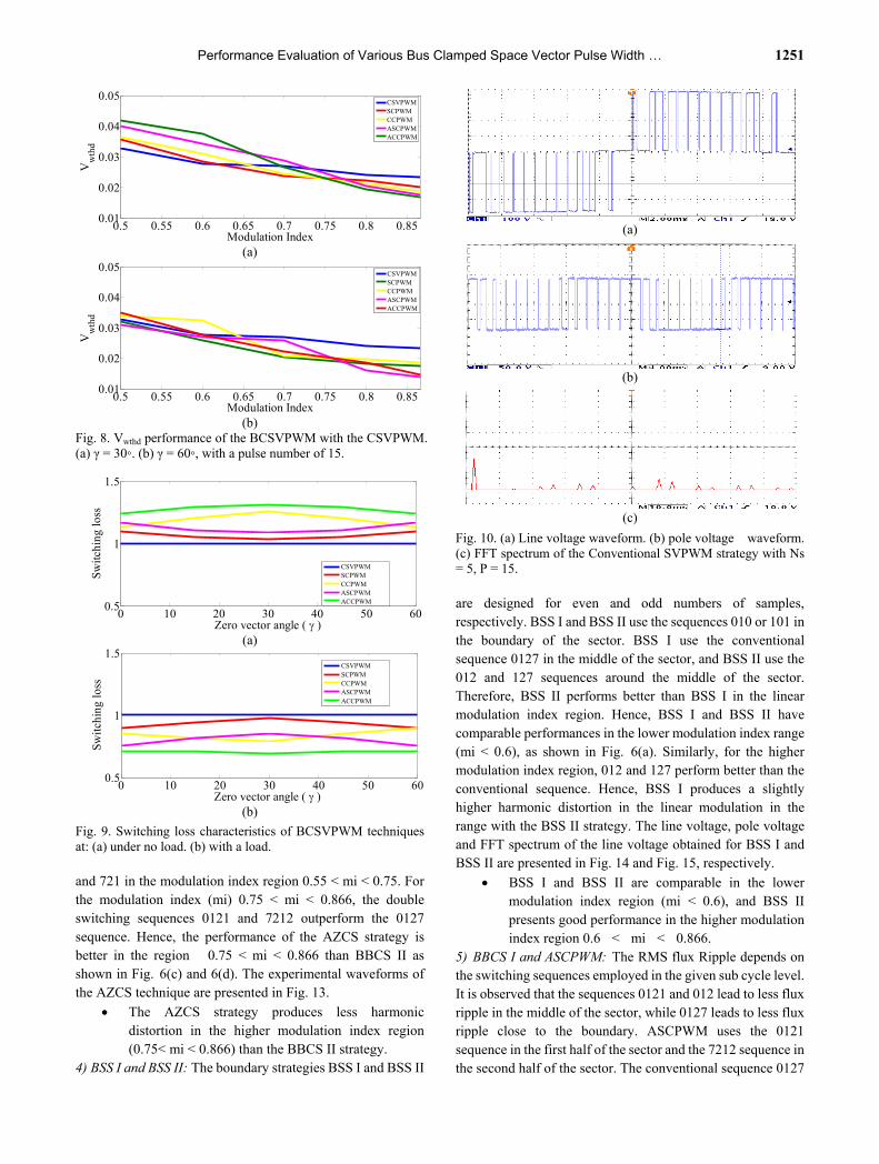
D. Variation of the THD Based on the Zero Vector Angle (γ)
The change in the position of the zero vector angle (γ) in a sector can change the location of the clamping of a phase in a half cycle period. If the clamping is continuous for the 600 duration the technique is referred to as the continual clamping technique (CCPWM). If the 600 clamping duration is split into two intervals, one with γ duration in the first quarter cycle and another with 600- γ in the next quarter cycle it is referred to as the split clamping technique (SCPWM) [6].
A Vwthd comparison of CSVPWM, SCPWM, CCPWM, ASCPWM and ACCPWM are presented in Fig. 8(a)-(b) for γ = 300 and γ = 600. The pulse number considered for the
Performance Evaluation of Various Bus Clamped Space Vector Pulse Width … 1253
(a)
(b)
(c)
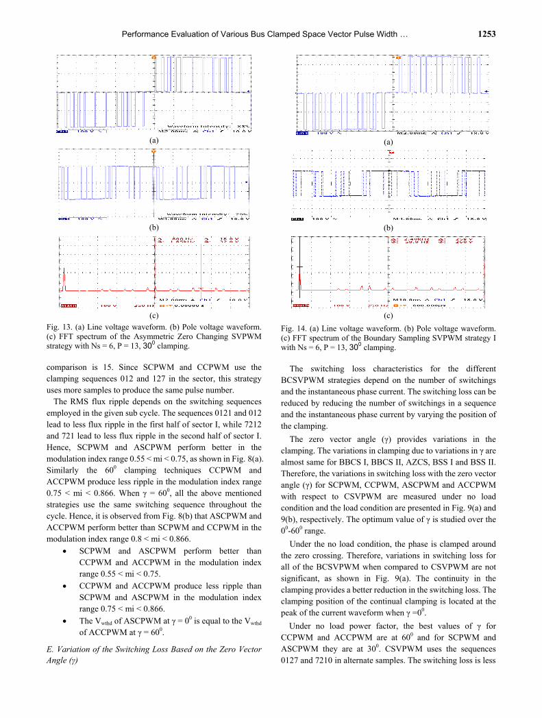
Fig. 13. (a) Line voltage waveform. (b) Pole voltage waveform. (c) FFT spectrum of the Asymmetric Zero Changing SVPWM strategy with Ns = 6, P = 13, 300 clamping.
comparison is 15. Since SCPWM and CCPWM use the clamping sequences 012 and 127 in the sector, this strategy uses more samples to produce the same pulse number. The RMS flux ripple depends on the switching sequences employed in the given sub cycle. The sequences 0121 and 012 lead to less flux ripple in the first half of sector I, while 7212 and 721 lead to less flux ripple in the second half of sector I. Hence, SCPWM and ASCPWM perform better in the modulation index range 0.55 < mi < 0.75, as shown in Fig. 8(a). Similarly the 600 clamping techniques CCPWM and ACCPWM produce less ripple in the modulation index range 0.75 < mi < 0.866. When γ = 600, all the above mentioned strategies use the same switching sequence throughout the cycle. Hence, it is observed from Fig. 8(b) that ASCPWM and ACCPWM perform better than SCPWM and CCPWM in the modulation index range 0.8 < mi < 0.866.
SCPWM and ASCPWM perform better than CCPWM and ACCPWM in the modulation index range 0.55 < mi < 0.75.
CCPWM and ACCPWM produce less ripple than SCPWM and ASCPWM in the modulation index range 0.75 < mi < 0.866.
The Vwthd of ASCPWM at γ = 00 is equal to the Vwthd of ACCPWM at γ = 600.
E. Variation of the Switching Loss Based on the Zero Vector Angle (γ)
(a)
(b)
(c)
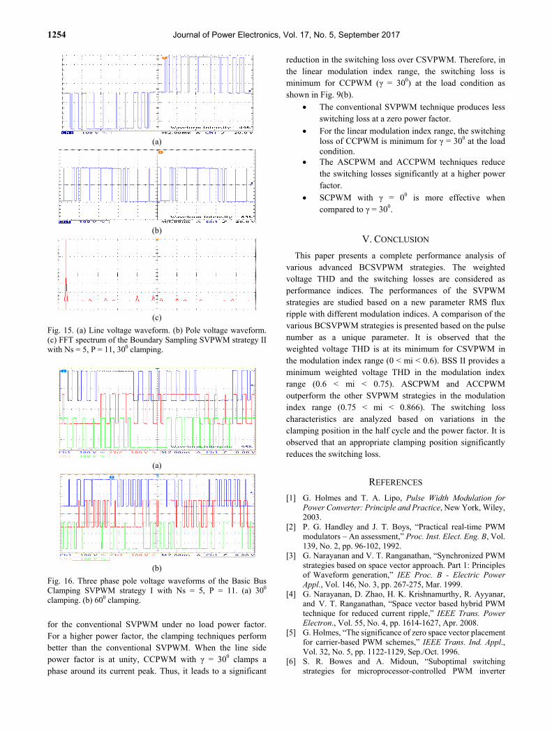
Fig. 14. (a) Line voltage waveform. (b) Pole voltage waveform. (c) FFT spectrum of the Boundary Sampling SVPWM strategy I with Ns = 6, P = 13, 300 clamping.
The switching loss characteristics for the different BCSVPWM strategies depend on the number of switchings and the instantaneous phase current. The switching loss can be reduced by reducing the number of switchings in a sequence and the instantaneous phase current by varying the position of the clamping.
The zero vector angle (γ) provides variations in the clamping. The variations in clamping due to variations in γ are almost same for BBCS I, BBCS II, AZCS, BSS I and BSS II. Therefore, the variations in switching loss with the zero vector angle (γ) for SCPWM, CCPWM, ASCPWM and ACCPWM with respect to CSVPWM are measured under no load condition and the load condition are presented in Fig. 9(a) and 9(b), respectively. The optimum value of γ is studied over the 00-600 range.
Under the no load condition, the phase is clamped around the zero crossing. Therefore, variations in switching loss for all of the BCSVPWM when compared to CSVPWM are not significant, as shown in Fig. 9(a). The continuity in the clamping provides a better reduction in the switching loss. The clamping position of the continual clamping is located at the peak of the current waveform when γ =00.
Under no load power factor, the best values of γ for CCPWM and ACCPWM are at 600 and for SCPWM and ASCPWM they are at 300. CSVPWM uses the sequences 0127 and 7210 in alternate samples. The switching loss is less
1254 Journal of Power Electronics, Vol. 17, No. 5, September 2017
(a)
(b)
(c)
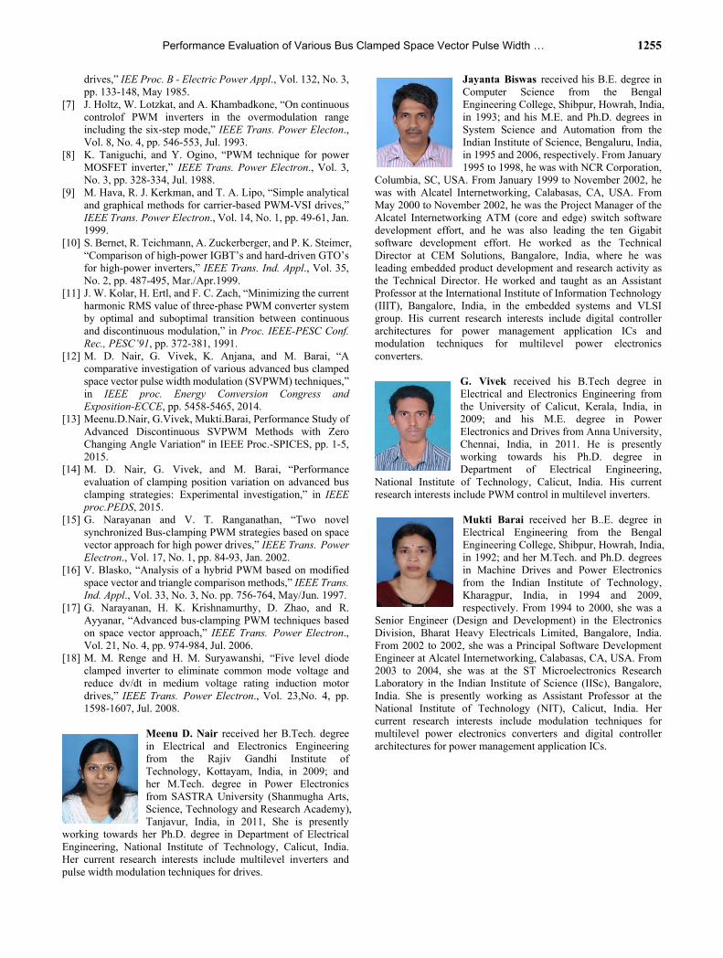
Fig. 15. (a) Line voltage waveform. (b) Pole voltage waveform. (c) FFT spectrum of the Boundary Sampling SVPWM strategy II with Ns = 5, P = 11, 300 clamping.
(a)
(b)
Fig. 16. Three phase pole voltage waveforms of the Basic Bus Clamping SVPWM strategy I with Ns = 5, P = 11. (a) 300 clamping. (b) 600 clamping.
for the conventional SVPWM under no load power factor. For a higher power factor, the clamping techniques perform better than the conventional SVPWM. When the line side power factor is at unity, CCPWM with γ = 300 clamps a phase around its current peak. Thus, it leads to a significant
reduction in the switching loss over CSVPWM. Therefore, in the linear modulation index range, the switching loss is minimum for CCPWM (γ = 300) at the load condition as shown in Fig. 9(b).
The conventional SVPWM technique produces less switching loss at a zero power factor.
For the linear modulation index range, the switching loss of CCPWM is minimum for γ = 300 at the load condition.
The ASCPWM and ACCPWM techniques reduce the switching losses significantly at a higher power factor.
SCPWM with γ = 00 is more effective when compared to γ = 300.
V. CONCLUSION
This paper presents a complete performance analysis of various advanced BCSVPWM strategies. The weighted voltage THD and the switching losses are considered as performance indices. The performances of the SVPWM strategies are studied based on a new parameter RMS flux ripple with different modulation indices. A comparison of the various BCSVPWM strategies is presented based on the pulse number as a unique parameter. It is observed that the weighted voltage THD is at its minimum for CSVPWM in the modulation index range (0 < mi < 0.6). BSS II provides a minimum weighted voltage THD in the modulation index range (0.6 < mi < 0.75). ASCPWM and ACCPWM outperform the other SVPWM strategies in the modulation index range (0.75 < mi < 0.866). The switching loss characteristics are analyzed based on variations in the clamping position in the half cycle and the power factor. It is observed that an appropriate clamping position significantly reduces the switching loss.
REFERENCES
[1] G. Holmes and T. A. Lipo, Pulse Width Modulation for Power Converter: Principle and Practice, New York, Wiley, 2003.
[2] P. G. Handley and J. T. Boys, “Practical real-time PWM modulators – An assessment,” Proc. Inst. Elect. Eng. B, Vol. 139, No. 2, pp. 96-102, 1992.
[3] G. Narayanan and V. T. Ranganathan, “Synchronized PWM strategies based on space vector approach. Part 1: Principles of Waveform generation,” IEE Proc. B - Electric Power Appl., Vol. 146, No. 3, pp. 267-275, Mar. 1999.
[4] G. Narayanan, D. Zhao, H. K. Krishnamurthy, R. Ayyanar, and V. T. Ranganathan, “Space vector based hybrid PWM technique for reduced current ripple,” IEEE Trans. Power Electron., Vol. 55, No. 4, pp. 1614-1627, Apr. 2008.
[5] G. Holmes, “The significance of zero space vector placement for carrier-based PWM schemes,” IEEE Trans. Ind. Appl., Vol. 32, No. 5, pp. 1122-1129, Sep./Oct. 1996.
[6] S. R. Bowes and A. Midoun, “Suboptimal switching strategies for microprocessor-controlled PWM inverter
Performance Evaluation of Various Bus Clamped Space Vector Pulse Width … 1255
drives,” IEE Proc. B - Electric Power Appl., Vol. 132, No. 3, pp. 133-148, May 1985.
[7] J. Holtz, W. Lotzkat, and A. Khambadkone, “On continuous controlof PWM inverters in the overmodulation range including the six-step mode,” IEEE Trans. Power Electon., Vol. 8, No. 4, pp. 546-553, Jul. 1993.
[8] K. Taniguchi, and Y. Ogino, “PWM technique for power MOSFET inverter,” IEEE Trans. Power Electron., Vol. 3, No. 3, pp. 328-334, Jul. 1988.
[9] M. Hava, R. J. Kerkman, and T. A. Lipo, “Simple analytical and graphical methods for carrier-based PWM-VSI drives,” IEEE Trans. Power Electron., Vol. 14, No. 1, pp. 49-61, Jan. 1999.
[10] S. Bernet, R. Teichmann, A. Zuckerberger, and P. K. Steimer, “Comparison of high-power IGBT’s and hard-driven GTO’s for high-power inverters,” IEEE Trans. Ind. Appl., Vol. 35, No. 2, pp. 487-495, Mar./Apr.1999.
[11] J. W. Kolar, H. Ertl, and F. C. Zach, “Minimizing the current harmonic RMS value of three-phase PWM converter system by optimal and suboptimal transition between continuous and discontinuous modulation,” in Proc. IEEE-PESC Conf. Rec., PESC’91, pp. 372-381, 1991.
[12] M. D. Nair, G. Vivek, K. Anjana, and M. Barai, “A comparative investigation of various advanced bus clamped space vector pulse width modulation (SVPWM) techniques,” in IEEE proc. Energy Conversion Congress and Exposition-ECCE, pp. 5458-5465, 2014.
[13] Meenu.D.Nair, G.Vivek, Mukti.Barai, Performance Study of Advanced Discontinuous SVPWM Methods with Zero Changing Angle Variation" in IEEE Proc.-SPICES, pp. 1-5, 2015.
[14] M. D. Nair, G. Vivek, and M. Barai, “Performance evaluation of clamping position variation on advanced bus clamping strategies: Experimental investigation,” in IEEE proc.PEDS, 2015.
[15] G. Narayanan and V. T. Ranganathan, “Two novel synchronized Bus-clamping PWM strategies based on space vector approach for high power drives,” IEEE Trans. Power Electron., Vol. 17, No. 1, pp. 84-93, Jan. 2002.
[16] V. Blasko, “Analysis of a hybrid PWM based on modified space vector and triangle comparison methods,” IEEE Trans. Ind. Appl., Vol. 33, No. 3, No. pp. 756-764, May/Jun. 1997.
[17] G. Narayanan, H. K. Krishnamurthy, D. Zhao, and R. Ayyanar, “Advanced bus-clamping PWM techniques based on space vector approach,” IEEE Trans. Power Electron., Vol. 21, No. 4, pp. 974-984, Jul. 2006.
[18] M. M. Renge and H. M. Suryawanshi, “Five level diode clamped inverter to eliminate common mode voltage and reduce dv/dt in medium voltage rating induction motor drives,” IEEE Trans. Power Electron., Vol. 23,No. 4, pp. 1598-1607, Jul. 2008.
Meenu D. Nair received her B.Tech. degree in Electrical and Electronics Engineering from the Rajiv Gandhi Institute of Technology, Kottayam, India, in 2009; and her M.Tech. degree in Power Electronics from SASTRA University (Shanmugha Arts, Science, Technology and Research Academy), Tanjavur, India, in 2011, She is presently
working towards her Ph.D. degree in Department of Electrical Engineering, National Institute of Technology, Calicut, India. Her current research interests include multilevel inverters and pulse width modulation techniques for drives.
Jayanta Biswas received his B.E. degree in Computer Science from the Bengal Engineering College, Shibpur, Howrah, India, in 1993; and his M.E. and Ph.D. degrees in System Science and Automation from the Indian Institute of Science, Bengaluru, India, in 1995 and 2006, respectively. From January 1995 to 1998, he was with NCR Corporation,
Columbia, SC, USA. From January 1999 to November 2002, he was with Alcatel Internetworking, Calabasas, CA, USA. From May 2000 to November 2002, he was the Project Manager of the Alcatel Internetworking ATM (core and edge) switch software development effort, and he was also leading the ten Gigabit software development effort. He worked as the Technical Director at CEM Solutions, Bangalore, India, where he was leading embedded product development and research activity as the Technical Director. He worked and taught as an Assistant Professor at the International Institute of Information Technology (IIIT), Bangalore, India, in the embedded systems and VLSI group. His current research interests include digital controller architectures for power management application ICs and modulation techniques for multilevel power electronics converters.
G. Vivek received his B.Tech degree in Electrical and Electronics Engineering from the University of Calicut, Kerala, India, in 2009; and his M.E. degree in Power Electronics and Drives from Anna University, Chennai, India, in 2011. He is presently working towards his Ph.D. degree in Department of Electrical Engineering,
National Institute of Technology, Calicut, India. His current research interests include PWM control in multilevel inverters.
Mukti Barai received her B..E. degree in Electrical Engineering from the Bengal Engineering College, Shibpur, Howrah, India, in 1992; and her M.Tech. and Ph.D. degrees in Machine Drives and Power Electronics from the Indian Institute of Technology, Kharagpur, India, in 1994 and 2009, respectively. From 1994 to 2000, she was a
Senior Engineer (Design and Development) in the Electronics Division, Bharat Heavy Electricals Limited, Bangalore, India. From 2002 to 2002, she was a Principal Software Development Engineer at Alcatel Internetworking, Calabasas, CA, USA. From 2003 to 2004, she was at the ST Microelectronics Research Laboratory in the Indian Institute of Science (IISc), Bangalore, India. She is presently working as Assistant Professor at the National Institute of Technology (NIT), Calicut, India. Her current research interests include modulation techniques for multilevel power electronics converters and digital controller architectures for power management application ICs.