Embed Size (px)
Citation preview

13
CHAPTER 2
MULTILEVEL INVERTERS
This chapter is a literature review which presents the state-of-art of
the different multilevel inverter topologies and modulation techniques to
understand the system research better. Although there are a large number of
multilevel inverter topologies in the literature, in this chapter only the most
common topologies are reviewed. The detailed advantages and disadvantages
of these multilevel inverter topologies are discussed in this chapter. Also, the
details on the impact of unbalanced load/source on multilevel inverter are
explained.
2.1 INTRODUCTION
Multilevel inverters continue to receive more and more attention
because of their high voltage operation capability, low switching losses, high
efficiency and low output of Electro Magnetic Interference (EMI). The term
multilevel starts with the three-level inverter introduced by Nabae et al
(1981). Nowadays, multilevel inverters are becoming increasingly popular in
power applications, as multilevel inverters have the ability to meet the
increasing demand of power rating and power quality associated with reduced
harmonic distortion and lower electromagnetic interference.
A multilevel inverter has several advantages over a conventional
two-level inverter that uses high switching frequency pulse width modulation
(PWM). The most attractive features of a multilevel inverter are as follows:

14
1) They can generate output voltages with extremely low
distortion and lower dv/dt.
2) They draw input current with very low distortion.
3) They generate smaller common-mode (CM) voltage.
4) They can operate with a lower switching frequency.
2.2 TOPOLOGY OF MULTILEVEL INVERTERS
Multilevel inverters have an arrangement of power switching
devices and capacitor voltage sources. Multilevel inverters are suitable for
high-voltage applications because of their ability to synthesize output voltage
waveforms with a better harmonic spectrum and attain higher voltages with a
limited maximum device rating.
There are three main types of multilevel inverters: diode-clamped
(neutral-clamped), capacitor-clamped (flying capacitors), and cascaded H-
bridge inverter.
Figure 2.1 Multilevel Inverter Topologies

15
2.2.1 Diode-Clamped Inverter
The diode-clamped inverter is also known as the neutral-point
clamped inverter (NPC) which was introduced by Nabae et al (1981). The
diode-clamped inverter consists of two pairs of series switches (upper and
lower) in parallel with two series capacitors where the anode of the upper
diode is connected to the midpoint (neutral) of the capacitors and its cathode
to the midpoint of the upper pair of switches; the cathode of the lower diode is
connected to the midpoint of the capacitors and divides the main DC voltage
into smaller voltages, which is shown in Figure 2.2. The middle point of the
two capacitors can be defined as the “neutral point”. The NPC uses a single
dc bus that is subdivided into a number of voltage levels by a series string of
capacitors. For a three-level diode-clamped inverter if the point O is taken as
the ground reference, the output voltage has three states 120, dcV and 1
2 dcV .
The line-line voltages of two legs with the capacitors are: 1 1
2 2, ,0,dc dc dcV V V ,
and dcV .Three phases are necessary to generate a three-phase voltage.
Figure 2.2 Shows a Two-Phase Diode-Clamped Multilevel Inverter

16
Some disadvantages of the diode-clamped multilevel inverter may
be observed that using extra diodes in series becomes impractical when the
number of levels n increases, requiring 1 2n n diodes per phase if all
the diodes have equal blocking voltages. Note that the voltages for diodes in
different positions are not balanced. For example, diode 2aD must block two
capacitor voltages, 2a nD must block 2n capacitor voltages. Also, the
switch duty cycle is different for some of the switches requiring different
current ratings. In addition, the capacitors do not share the same discharge or
charge current resulting in a voltage imbalance of the series capacitors. The
capacitor voltage imbalance can be controlled by using a back-to-back
topology, connecting resistors in parallel with capacitors, or using redundant
voltage states which were introduced by Nabae et al (1981).
The five-level output voltage can be generated by controlling the
switches. Table 2.1 shows the proper switching states. The switches
( 1aS and 1aS ), and ( 2aS and 2aS ) are complementary pairs. When 1aS is on
( 1 1aS ), 1aS is off ( 1 0aS ). Other switch pairs are similar. When the
switches 1aS , 2aS , 1bS and 2bS are off and 2aS , 1bS and 2bS are on, the
corresponding output voltage for each phase of the diode-clamped multilevel
inverter are 12 dcV and 1
2 dcV . The phase to phase output voltage is dcV .
Similarly, the output voltages for other switching stages are shown in
Table 2.1.
The advantages for the diode-clamped inverter are,
(1) A large number of levels ‘n’ yields a small harmonic
distortion.
(2) All of the phases share a common dc bus.

17
(3) Reactive power flow can be controlled.
(4) High efficiency for fundamental switching frequency.
(5) Relatively simple control methods.
The disadvantages are,
(1) Different voltage ratings for clamping diodes are required.
(2) Real power flow is difficult because of the capacitors
imbalance.
(3) Need high voltage rating diodes to block the reverse voltages.
(4) The number of switches, capacitors, and diodes required in
the circuit increases with the increase in the number of output
voltage levels. Extra clamping diodes required are
1 2n n per phase.
Table 2.1 Switch States and the Output Voltages for Diode-Clamped
Multilevel Inverter
Sa1 Sa2 Sa1' Sa2' Sb1 Sb2 Sb1' Sb2' Vao Vbo Vab
0 0 1 1 1 1 0 0 dcV2
dcV2 dc -V
0 0 1 1 0 1 1 0 dcV2
0 dcV2
1 1 0 0 1 1 0 0 dcV2
dcV2
0
0 0 1 1 0 0 1 1 dcV2
dcV2
0
0 1 1 0 0 0 1 1 0 dcV2
dcV2
1 1 0 0 0 0 1 1 dcV2
dcV2 dcV

18
2.2.2 Capacitor-Clamped Inverter
The capacitor-clamped multilevel inverter known as flying
capacitor is similar to the diode-clamped inverter was presented in Hochgraf
et al (1994) and Lai et al (1996). The capacitor-clamped multilevel inverter
topology provides more flexibility in waveform synthesis and balancing
voltage. In capacitor-clamped inverter, the diode in the diode-clamped
topology is replaced by clamping capacitors or floating capacitors to clamp
the voltages. Each phase-leg has an identical structure. The size of the voltage
increment between two capacitors determines the size of the voltage levels in
the output waveform.
Capacitor-clamped multilevel inverter topologies are relatively new
compared to the diode-clamped or the cascaded H-bridge cell inverter
topologies. Redundancy in the switching states is available by using flying
capacitors instead of clamping diodes. This redundancy can be used to
regulate the capacitor voltages and obtain the same desired level of voltage at
the output. Figure 2.3 shows a single-phase five-level capacitor-clamped
multilevel inverter topology. The voltage across the capacitors is considered
to be half of DC source voltage dcV . The output voltage consists of five
different voltage levels, , ( / 2), 0, ( / 2)dc dc dcV V V and dcV .
Similar to the other multilevel inverter topologies, capacitor-
clamped multilevel inverter also has complementary pairs of switches. In the
present circuit considered, switches 1aS & 1aS and 2aS & 2aS are
complementary to each other. The number of switching states for the
capacitor-clamped multilevel inverter topology is higher than that of the
diode-clamped inverter. The number of voltage levels at the output can be
increased by adding a pair of complementary switches and a capacitor. An
output voltage can be produced by using different combinations of switches.

19
The topology allows increased flexibility in how the majority of the voltage
levels may be chosen. In addition, the switches may be chosen to charge or
discharge the clamped capacitors, which balance the capacitor voltage.
The general n -level capacitor-clamped multilevel inverter has an n-
level output phase voltage. Thus, two phases would produce a 2 1n level
output voltage, or line voltage, which is shown in Figure 2.4. Similar to the
diode-clamped multilevel inverter, the capacitors have different ratings.
However, the arrangement requires a large number of capacitors per phase 1
2 1 2n n which results in a bulky and expensive inverter when
compared to the diode-clamped inverter.
Figure 2.3 Topology of a Capacitor-Clamped Multilevel Inverter
The advantages of the capacitor-clamped multilevel inverter are,
(1) Large ‘n’ allows the capacitors extra energy during long discharge transient.
(2) Phase redundancies are available for balancing the voltage levels of the capacitors.

20
(3) Lower Total Harmonic Distortion when the number of levels ‘n’ is high.
(4) Active and Reactive power flow can be controlled.
The disadvantages are,
(1) Large numbers of capacitors are bulky and more expensive
than the clamping diodes used in the diode-clamped
multilevel inverter.
(2) Complex control is required to maintain the capacitor’s
voltage balance.
(3) Switching utilization and Efficiency are poor for real power
transmission.
Figure 2.4 Two-Phase Capacitor-Clamped Multilevel Inverter

21
When the switches 1aS , 2aS , 1bS and 2bS are off and 1aS , 2aS , 1bS
and 2bS are on, the corresponding output voltage for each phase of the
capacitor-clamped multilevel inverter is 12 dcV and 1
2 dcV . The phase to phase
output voltage is dcV . Similarly, the output voltages for other switching stages
are shown in Table 2.2.
Table 2.2 Switch States and the Output Voltages for Capacitor-Clamped
Multilevel Inverter
Sa1 Sa2 Sa1' Sa2' Sb1 Sb2 Sb1' Sb2' Vao Vbo Vab
0 0 1 1 1 1 0 0 dcV2
dcV2 dcV
0 0 1 1 0 1 1 0 dcV2
0 dcV2
0 1 1 0 1 1 0 0 0 dcV2
dcV2
1 0 0 1 1 1 0 0 0 dcV2
dcV2
1 1 0 0 1 1 0 0 dcV2
dcV2
0
0 0 1 1 0 0 1 1 dcV2
dcV2
0
0 1 1 0 0 0 1 1 0 dcV2
dcV2
1 1 0 0 0 1 1 0 dcV2
0 dcV2
1 0 0 1 0 0 1 1 0 dcV2
dcV2
1 1 0 0 0 0 1 1 dcV2
dcV2 dcV
22
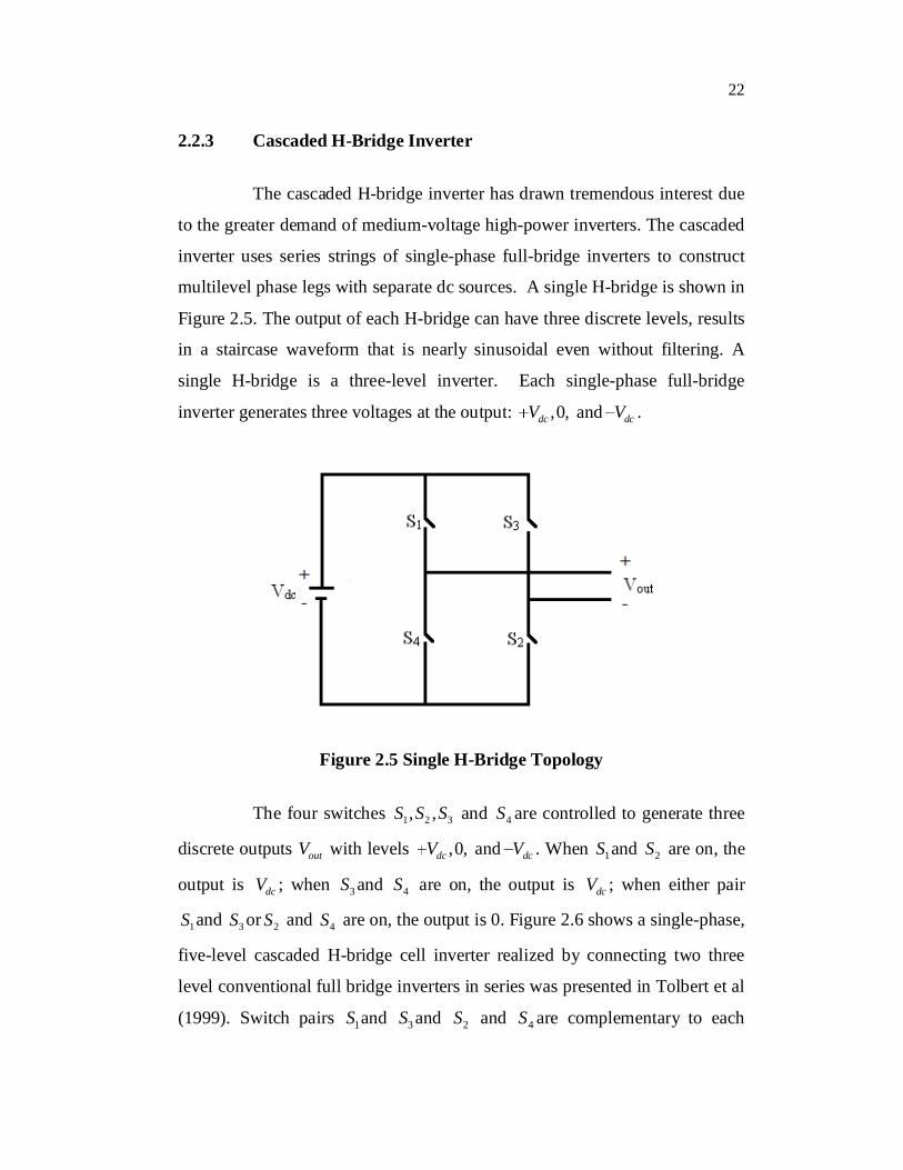
2.2.3 Cascaded H-Bridge Inverter
The cascaded H-bridge inverter has drawn tremendous interest due
to the greater demand of medium-voltage high-power inverters. The cascaded
inverter uses series strings of single-phase full-bridge inverters to construct
multilevel phase legs with separate dc sources. A single H-bridge is shown in
Figure 2.5. The output of each H-bridge can have three discrete levels, results
in a staircase waveform that is nearly sinusoidal even without filtering. A
single H-bridge is a three-level inverter. Each single-phase full-bridge
inverter generates three voltages at the output: ,0,dcV and dcV .
Figure 2.5 Single H-Bridge Topology
The four switches 1 2 3, ,S S S and 4S are controlled to generate three
discrete outputs outV with levels ,0,dcV and dcV . When 1S and 2S are on, the
output is dcV ; when 3S and 4S are on, the output is dcV ; when either pair
1S and 3S or 2S and 4S are on, the output is 0. Figure 2.6 shows a single-phase,
five-level cascaded H-bridge cell inverter realized by connecting two three
level conventional full bridge inverters in series was presented in Tolbert et al
(1999). Switch pairs 1S and 3S and 2S and 4S are complementary to each

23
other. The switching states are as shown in Table 1.2. The different voltage
levels that can be obtained at the output terminals are
2 , ,0,dc dc dcV V V and 2 dcV . If the dc voltage sources in both the inverter
circuits connected in series are not equal to each other, then nine levels can be
obtained at the output terminals. The number of levels in the output voltage
can be increased by two by adding an identical inverter in series. The n
number of output phase voltage levels in a cascaded inverter with s separate
dc sources is 2 1n s possible levels.
Figure 2.6 Five-Level Cascaded H-Bridge- Inverter
Cascaded H-bridge cell inverters use the least number of power
electronic devices when compared to any other topology. However, they
require isolated power sources in each cell which in turn requires a large
isolating transformer.

24
When the switches 1aS , 2aS , 3bS and 4bS are on and 3aS , 4aS , 1bS and
2bS are off, the corresponding output voltage of the cascaded H-bridge
multilevel inverter is zero. The switches 1aS , 2aS , 1bS and 2bS are on and
3aS , 4aS , 3bS and 4bS are off, the corresponding output voltage of the cascaded
H-bridge multilevel inverter is dc2V . Similarly, the output voltages for other
switching stages are shown in Table 2.3.
Table 2.3 Possible Switching States for Cascaded H-Bridge Cell Inverter
Sa1 Sa2 Sa3 Sa4 Sb1 Sb2 Sb3 Sb4 Vab
1 1 0 0 0 0 1 1 0
1 0 0 1 1 0 0 1 0
1 0 0 1 0 1 1 0 0
0 1 1 0 1 0 0 1 0
0 1 1 0 0 1 1 0 0
0 0 1 1 1 1 0 0 0
1 1 0 0 1 0 0 1 dcV
1 1 0 0 0 1 1 0 dcV
1 0 0 1 1 1 0 0 dcV
0 1 1 0 1 1 0 0 dcV
1 1 0 0 1 1 0 0 dc2V
0 0 1 1 1 0 0 1 dc-V
0 0 1 1 0 1 1 0 dc-V
1 0 0 1 0 0 1 1 dc-V
0 1 1 0 0 0 1 1 dc-V
0 0 1 1 0 0 1 1 dc-2V

25
The advantages for cascaded multilevel H-bridge inverter are the
following:
(1) The series structure allows a scalable, modularized circuit
layout and packaging due to the identical structure of each H-
bridge.
(2) No extra clamping diodes or voltage balancing capacitors are
necessary.
(3) Switching redundancy for inner voltage levels is possible
because the phase voltage is the sum of the output of each
bridge.
The disadvantage for cascaded multilevel H-bridge inverter is the
following:
(1) Needs separate DC sources.
Figure 2.7 Staircase Sinusoidal Waveform Generated by Cascaded
H-Bridge Multilevel Inverter

26
2.3 CONTROL AND MODULATION TECHNIQUES OF
MULTILEVEL INVERTERS
2.3.1 Classification of Modulation Strategies
The modulation methods used in multilevel inverters can be
classified according to the switching frequency was discussed in Rodriguez et
al (2002), Celanovic and Boroyevic (2001) and Rodriguez et al (2001).
Modulation techniques that work with high switching frequencies have many
commutations for the power semiconductors in a cycle of the fundamental
output voltage. Multilevel inverters generate sinusoidal voltages from discrete
voltage levels, and Pulse Width-Modulation (PWM) strategies accomplish
this task of generating sinusoids of variable voltages and frequencies. Several
techniques for the implementation of PWM for multilevel inverters have been
developed.
The well known high switching frequency methods are classic
carrier based Sinusoidal PWM (SPWM) was presented in Tolbert and
Habetler (1999) and Hammond (1997) and Space Vector PWM. The popular
methods for low switching frequency methods are Space Vector Modulation
(SVM) method and selective harmonic elimination method.
Figure 2.8 Classification of Multilevel Modulation Methods
27
A very popular technique with high switching frequency in
industrial applications is the classic carrier-based Sinusoidal PWM (SPWM)
that uses the phase-shifting technique to increase the effective switching
frequency. Therefore, the harmonics in the load voltage can be reduced was
proposed by Liang and Nwankpa (1999). Space Vector Modulation (SVM)
has been used in three-level inverters was presented in Celanovic and
Boroyevic (2001). Control techniques that work with low switching
frequencies generally perform one or two commutations of the power
semiconductors during a cycle of the output voltages, generating a staircase
waveform. Representatives of this family are the multilevel selective
harmonic elimination was presented in Li et al (2000) and Sirisukprasert et al
(2002) based on elimination theory presented was presented in Enjeti et al
(1990), Patel and Hoft (1973) & (1974) and the Space Vector Control (SVC)
was first introduced by Rodriguez et al (2000).
The three multilevel modulation methods most discussed are
multilevel carrier-based sinusoidal PWM, selective harmonic elimination, and
multilevel space vector PWM; all are extensions of traditional two-level
modulation strategies to several levels. Other methods have been used to a
much lesser extent by researchers; therefore, only these three major
techniques are discussed.
2.3.2 Multilevel SPWM
Multilevel SPWM needs multiple carriers. Several multicarrier
techniques have been developed to reduce distortion in multilevel inverters,
based on the classical SPWM with triangular carriers. Some methods use
carrier disposition and others use phase shifting of multiple carrier signals
was presented in Lai and Peng (1996), Tolbert and Habetler (1999),
Mwinyiwiwa et al (1998) and Agelidis and Calais (1998).

28
(a)
(b)
Figure 2.9 Multi-Carrier Control (a) Control Signal and Carrier
signals; (b) Output Voltage
The Multilevel SPWM method is the extension of bi-level SPWM.
One reference signal is used to compare the carriers which is shown in Figure

29
2.9 (a). If the reference signal is higher than the carrier, the corresponding
inverter cell outputs positive voltage, otherwise, the corresponding inverter
cell outputs negative voltage. The output voltage of the inverter is shown in
Figure 2.9 (b).
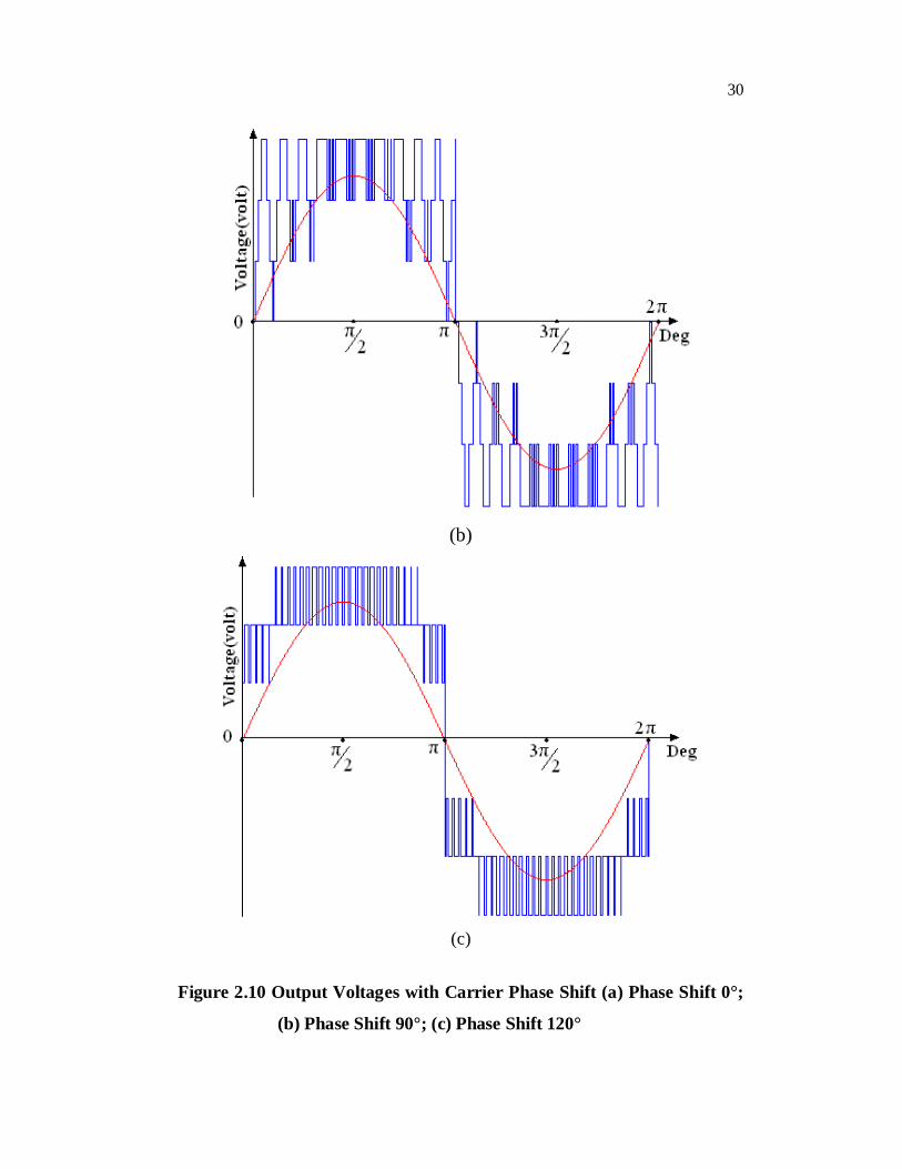
A number of cascaded cells in one phase with their carriers shifted
by an angle and using the same control voltage produce a load voltage with
the smallest distortion was discussed in Liang and Nwankpa (1999). The
effect of this carrier phase-shifting technique can be clearly observed in
Figure 2.10. This result has been obtained for the multi-cell inverter in a
seven-level configuration, which uses three series-connected cells in each
phase. The smallest distortion is obtained when the carriers are shifted by an
angle of 120°.
(a)
Figure 2.10 (Continued)
30
(b)
(c)
Figure 2.10 Output Voltages with Carrier Phase Shift (a) Phase Shift 0°;
(b) Phase Shift 90°; (c) Phase Shift 120°
31
A very common practice in industrial applications for the multilevel
inverter is the injection of a third harmonic in each cell to increase the output
voltage was discussed in Hammond (1997) and Hill and Harbourt (1999).
Another advantageous feature of multilevel SPWM is that the effective
switching frequency of the load voltage is much higher than the switching
frequency of each cell, as determined by its carrier signal. This property
allows a reduction in the switching frequency of each cell, thus reducing the
switching losses.
The advantage of the method is that it is very simple. But it has two
disadvantages. The first method cannot completely eliminate the low order
harmonics. Therefore the low order harmonics cause loss and high filter
requirements. The second method is the high switching frequency which
causes high switching loss and low efficiency.
2.3.3 Space Vector Modulation (SVM)
The SVM technique can be easily extended to all multilevel
inverters. Figure 2.11 shows space vector diagrams for the traditional three-level,
five-level, and seven-level inverters. Space vector diagrams are universal
regardless of the type of multilevel inverter was presented in Lee et al (1998), Li et
al (2000), Holmes and McGrath (2001) and Kang et al (2000). Therefore it can be
used for diode-clamped, capacitor-clamped or cascaded inverters.
The SVM generate the output voltage as the weighted mean of the
three vectors adjacent to the reference in the d-q plane. SVM involves
synthesizing the reference voltage space vector by switching among the three
nearest voltage space vectors. The adjacent three vectors can synthesize a
desired voltage vector by computing the duty cycle for each vector according
to the following:

32
1 1 2 2j j j j j jT V T V T VV
T (2.1)
Generally Space-Vector PWM methods have the following
advantages,
1) Good utilization of DC-link voltage, low current ripple.
2) Relatively easy control and hardware implementation by a Digital Signal Processor (DSP).
3) Flexibility in optimizing switching waveforms and has
relatively good performance at low modulation ratio.
The Disadvantages of SVM are
1. As the number of levels increases, redundant switching states and the complexity of selecting switching states increase dramatically was addressed in Jose Rodriguez et al (2002).
2. It cannot completely eliminate the low order harmonics.
(a)
Figure 2.11 (Continued)

33
(b)
(c)
Figure 2.11 Space Vector Diagram (a) Three-Level; (b) Five-Level;
(c) Seven-Level

34
Li et al (2000) has used decomposition of the five-level space-
vector diagram into two three-level space-vector diagrams with a phase shift
to minimize ripples and simplify control. Also SVM cannot be applied to
multilevel inverters with unequal dc sources.
2.3.4 Selective Harmonics Elimination
The selective harmonics elimination method is based on the
harmonic elimination theory was developed by Patel and Hoft (1973) and
(1974). A multilevel inverter can produce a quarter-wave symmetric stepped
voltage waveform synthesized by several DC voltages as shown in Figure 2.7.
By applying Fourier series analysis, the output voltage can be
expressed as
1 1 2 21,3,5..
4 cos cos ... cos sink kn
V t V n V n V n n tn
(2.2)
where k is the number of DC sources, and 1V , 2V … kV are the level of DC
voltages. The switching angles must satisfy the condition
1 20 ......2k . However, if the switching angles do not satisfy
the condition, this method no longer exists. If 21 .... kV V V , then this is
called equal DC voltages sources.
To minimize harmonic distortion and to achieve adjustable
amplitude of the fundamental component, up to k-1 harmonic contents can be
removed from the voltage waveform. In general, the most significant low-
frequency harmonics are eliminated by properly selecting angles among
different level inverters, and high-frequency harmonic components can be
removed by using additional filter circuits. The output is a staircase waveform
with steps angle duration optimized to cancel the specified harmonics;

35
however, the number of harmonics that can be eliminated at the same time is
proportional to the number of inverter levels.
To keep the number of eliminated harmonics at a constant level, all
switching angles must satisfy the condition 1 20 ......2k , or the
THD increases dramatically. However, if the switching angles do not satisfy
the condition, this scheme no longer exists. Due to this reason, this
modulation strategy basically provides a narrow range of modulation index,
which is one of its disadvantages was presented in Jose Rodriguez et al
(2002). In a seven-level equally stepped waveform, the modulation index is
only available from 0.5 to 1.05. At modulation indexes lower than 0.5, if this
scheme is applied, the allowable harmonic components to be eliminated will
reduce from 2 to 1. The THD increases correspondingly.
Therefore, the modulation control problem is converted into a
mathematic problem to solve the following equations for a three-phase
system. Here, the fundamental peak value of the output voltage of 1V should
be controlled, and the 5th and 7th order harmonics should be eliminated. The
resulting harmonic equations are:
1 1 2 2 3 3cos cos cos ... cosk k mV n V n V n V n
1 1 2 2 3 3 0cos 5 cos 5 cos 5 ... cos 5k kV V V V and
1 1 2 2 3 3 0cos 7 cos 7 cos 7 ... cos 7k kV V V V (2.3)
where, m is modulation index defined as
1
4 dc
VmV (2.4)

36
When the selective harmonic elimination method is used, all of the
DC voltages are typically involved, where all of the switches are turned “on”
and “off” only once per fundamental cycle. The selective harmonic
elimination method also refers exactly to one switching pattern. The number
of switching angles is equal to the number of DC sources for selective
harmonic elimination method was discussed in McKenzie (2004).
The major difficulty for selective harmonic elimination method is
to solve the transcendental equations given in Equation. 2.3 for calculating
switching angles. The selective harmonic elimination method can eliminate
the number of harmonics not more than the number of the switching angles in
the transcendental equations. The solutions are not available for the whole
modulation index range, and it does not eliminate any number of specified
harmonics to satisfy the application requirements and control of multilevel
inverters with unequal DC source voltages which are impractical.
Recently, the resultant method has been proposed by Chiasson et al
(2003) and Chiasson et al (2004) to solve the transcendental equations for
switching angles. The transcendental equations characterizing the harmonic
content can be converted into polynomial equations. Elimination of harmonics
using resultant theory has been employed by McKenzie (2004) to determine
the switching angles to eliminate specific harmonics, such as the 5th, 7th, 11th,
and 13th. However, as the number of DC voltages or the number of switching
angle increase, the degrees of the polynomials in these equations are large and
it is difficult to solve the system of polynomial equations by using resultant
theory was proposed by Chiasson et al (2003).
2.4 IMPACTS OF UNBALANCED LOAD / SOURCE
Load condition has great impacts on the design and performance of
power inverters, as well as utility applications. In most of the cases, a power
37
inverter is designed under the assumption of a balanced load/source. Although
unbalanced loads and unbalanced sources seem to be abnormal conditions, in
real-time unbalanced loads and unbalanced sources are prevalent was
presented in Zhang (1998). Unbalanced source and load have been analyzed
extensively in power systems were discussed in Kusko and Peeran (1990).
Unbalanced loads are prevalent for UPS, stand alone power generation
applications, and for fault-mode operation of a balanced three-phase system
as well was presented in Kusko and Peeran (1990).
Unbalanced three phase source could also exist due to heavily
unbalanced loads. Unbalanced load or source may cause an overheated neutral
conductor due to excessive neutral current, low frequency reactive power, and
distorted source. Especially for UPS and stand alone power generation
applications, there is no limitation to the percentage of unbalance. Unbalanced
load condition for each phase can range from full load to no load, depending
on particular applications and the users demand. In a three-phase system, load
imbalance could be caused by unevenly distributed single-phase load or by
balanced three-phase load running at a fault condition, such as phase open or
short fault. The source imbalance may be caused by a large load imbalance
and non-uniform source output impedance. An unbalanced load may have
different load current rms levels among phases, or same load current rms levels but different phases, or both.
When imbalance happens with the load, the line-to-line current will
be unbalanced. Flowing through the source impedance, the unbalanced line-
to-line current will in turn cause the terminal voltage to be unbalanced. Due to
the elimination of the neutral point, the zero-sequence component will be
trapped within the source or the load, and zero-sequence current does not
exist from the source to the load. The impact of the load imbalance is only
reflected by a negative-sequence current from the source to the load. Thus, a
ripple power will be circulating between the source and the load at two times

38
of the line frequency. Since the neutral points are floating, the voltage
potentials of the neutral points will shift according to the unbalanced load was
addressed in Zhang et al (1998). This may cause ground current due to
unequal neutral potentials between the source and the load, and more severe
EMI problems. An unbalanced load/source can produce negative-sequence
current and zero-sequence current in the inverter depending on the source and
load connection. The negative sequence current draws 2W ripple power from
the source. The zero-sequence current flows through the neutral conductor.
2.5 SUMMARY
In this chapter, several multilevel inverter topologies were
discussed in more detail. Many different multilevel inverter topologies have
been proposed, the most commonly used are diode-clamped, capacitor-
clamped and cascaded H-bridge inverters were discussed. Following the
discussion on multilevel inverter topologies, several control and modulation
strategies were discussed. More specifically, the multilevel SPWM, Space
Vector Pulse Width Modulation, Selective Harmonic Elimination switching
schemes were presented. The advantages and disadvantages of various
multilevel inverter topologies and control techniques were also discussed.
Finally, a brief overview of the impact of unbalanced load/ source on the
performance of multilevel inverter has been discussed.
The purpose of the previous chapter was to provide both an
introduction to multilevel inverters as well as some background information
regarding other research concerning the multilevel inverter. The next chapter
provides more detailed explanation of cascaded H-bridge multilevel inverter with
separate dc sources. Furthermore, switching schemes like Bipolar Programmed
PWM, Unipolar Programmed PWM and Virtual Stage PWM switching schemes
are discussed. The idea of using unequal dc sources with multilevel inverters was
presented, followed by the concept of “duty cycle swapping.”