Embed Size (px)
Citation preview

LAB 6: ALU Design Design and Implementation of a
4-bit Arithmetic Logic Unit
November 8, 2002

2
Table of Contents Goals and Background……………………………………………………3 Task 1: Designing the 2:1 MUX……………………..……………………5 Task 2: Designing the Logic Unit…………………………………………6 Task 3: Designing the Arithmetic Unit…………………………………...8 Task 4: Compiling the 1-bit ALU………………………………………..15 Task 5: Compiling the 4-bit ALU………………...……………………...16 Task 6: Main Decoder Design…………………….……………………...18 Task 7: Designing the Display Switch Circuit…..………………………23 Task 8: Testing the Entire System……………….………………………24 Task 9: Timing & Speed of our 4-bit ALU System..……………………26 Discussion of Results & Conclusion…………...………………………....27

3
Goals and Background
A purpose of this lab is to design, implement and experimentally check a 4-bit Arithmetic Logic Unit (ALU). An ALU is a combinational circuit that performs arithmetic and logic operations on a pair of n-bit operands. The operations performed by an ALU are controlled by a set of function-select inputs. In this lab we will create a 4-bit ALU with 3 function-select inputs: Mode M, Select S1 and S0 inputs. The mode input (M) selects between a Logic (M=0) and an Arithmetic (M=1) operation. The functions performed by the ALU are given in the below table.
Table 1: Functions of ALU
M = 0 Logic S1 S0 C0 FUNCTION OPERATION (bit wise) 0 0 X AiBi AND 0 1 X Ai + Bi OR 1 0 X Ai⊕ Bi XOR 1 1 X (Ai⊕ Bi)’ XNOR
M = 1 Arithmetic S1 S0 C0 FUNCTION OPERATION 0 0 0 A Transfer A 0 0 1 A + 1 Increment A by 1 0 1 0 A + B Add A and B 0 1 1 A + B + 1 Increment the sum of A and B by 1 1 0 0 A + B' A plus one's complement of B 1 0 1 A – B Subtract B from A (i.e. B' + A + 1) 1 1 0 A' + B B plus one's complement of A 1 1 1 B – A B minus A (or A' + B + 1)
Table 1: Functions of ALU on individual bits
The numbers we will use will be inputted and displayed in two’s complement form. This form was chosen because it is easier and more accurate to execute arithmetic operations this way. However there is a potential for overflow, which is dealt with by using an overflow detector (V) in the circuit. This will be explained in greater detail later.
The block diagram for a 4-bit ALU can be seen below along with the given implementation method:

4
Figure 1: 4-bit ALU with Accompanying Implementation and Display Units
In order to begin designing this system of combinational circuits we first had to decide how the ALU will work. One option was to write out the full truth table and derive equations for F and V from that. The other option, which we chose to execute, was to design a 1-bit ALU, and then combine four of them to create a 4-bit ALU. Since the output of the 4-bit ALU (F[3:0]) is dependant on the signal M, we have two ways of displaying our results. When M=0, and the result from the 4-bit ALU is Logic based, the result is displayed on an array of LEDs. On the other hand, when M=1, the output of the 4-bit ALU is a 2’s complement digit. Using a decoder, we can display this digit’s sign and magnitude on a 7-segment display. However, because the four 7-segment displays on our Spartan XL board are linked together, we must create a Display Switch Circuit that alternates displaying the resulting sign and magnitude.
5
Section I – Designing the Bit-Slice ALU (1-bit) In order to design a bit-slice ALU, we needed to design three components: the arithmetic unit, the logic unit, and the 2:1 MUX which combines them and outputs the value specified by the Select bit (M). A block diagram of the entire unit is seen below.
Figure 2: Block Diagram of bit-slice ALU
Task 1 – Designing the 2:1 MUX
The function of this component is to select either G or H based on the value of M. We designed this multiplexer using VHDL code, and created a macro from it. The code can be seen below:
VHDL Code for 2:1 MUX
library IEEE; use IEEE.std_logic_1164.all; entity mux21 is port ( G: in STD_LOGIC; H: in STD_LOGIC; M: in STD_LOGIC; F: out STD_LOGIC; ); end mux21; architecture mux21_arch of mux21 is begin -- <<enter your statements here>> F <= (M and G) or ((not M) and H); end mux21_arch;

6
Our macro was then tested using Functional Simulation in Xilinx Foundation Software.
Figure 2: Functional Simulation of 2:1 MUX
Analysis of this waveform verifies that our multiplexer works properly since the output F takes the value of H when M=0, and G when M=1.
Task 2 – Designing the Logic Unit
Using the Logic segment of Table 1, we created the VHDL code for our Logic Unit. The code resembles a multiplexer with additional gates already factored in. Our VHDL Code is shown below, combined with a screen capture of it.
VHDL Code for the Logic Unit library IEEE; use IEEE.std_logic_1164.all; entity LOGIC is port ( A: in STD_LOGIC; B: in STD_LOGIC; S1: in STD_LOGIC; S0: in STD_LOGIC; H: out STD_LOGIC; ); end LOGIC; architecture LOGIC_arch of LOGIC is begin -- <<enter your statements here>> H <= ((not S1) and (not S0) and A and B) or ((not S1) and S0 and (A or B)) or (S1 and (not SO) and (A xor B)) or (S1 and S0 and (A xnor B)); end LOGIC_arch;

7
Figure 3: Screen Capture of HDL code for our Logic Unit (LOGIC)
In order to verify that the LOGIC macro we created based on the codes above functions properly, we performed Functional Simulation on it. The waveform generated is shown below:
Figure 4: Functional Simulation of Logic Macro
Analysis of this waveform successfully verifies that our Logic Unit functions properly. The S1 Bus in Figure 4 displays the hexadecimal values which are assigned to the certain logic operations in Table 1. A reference table is below:
Hex Value Binary Value S1 S0
0 0 0 1 0 1 2 1 0 3 1 1
Table 2: Reference Table for Figure 4

8
Task 3- Designing the Arithmetic Unit
The Arithmetic Unit can be designed by using a Full Adder and two additional components for A and B logic, which modifies the inputs A and B in such a way the Full Adder performs what it is assigned to do in the Arithmetic segment of Table 1.
Figure 5: Schematic Block Diagram of the Arithmetic Unit
a. Designing the A Logic Unit
In order to design the A-logic unit, we had to develop an equation that gives the values of Xi as a function of S1, S0 and Ai. To design this we used a truth table to solve for the expected values of Xi.
S1 S0 Ai Xi (A Logic) 0 0 0 0 0 0 1 1 0 1 0 0 0 1 1 1 1 0 0 0 1 0 1 1 1 1 0 1 1 1 1 0
Table 3: A-Logic Table K-map:
Xi S0 0 1 1 0 S1 0 1 0 1 Ai
Equations:
Xi = S1’Ai + S0’Ai + S1S0Ai’
Our next step was to write the VHDL code based on the equation above to create the A-logic macro. The VHDL code can be seen below:

9
VHDL Code for A-Logic Block library IEEE; use IEEE.std_logic_1164.all; entity alogic is port ( Ai: in STD_LOGIC; S1: in STD_LOGIC; S0: in STD_LOGIC; X: out STD_LOGIC; ); end alogic; architecture alogic_arch of alogic is begin -- <<enter your statements here>> X <= (S1 and S0) xor (Ai); end alogic_arch;
Figure 6: Schematic Capture of VHDL Code of A-Logic macro
We then tested our A-logic macro in order to verify that it worked properly. The Functional Simulation generated using Xilinx Foundation Software is pictured below:

10
Figure 7: Functional Simulation of A-Logic Macro
Comparing the output X to those in Table 3, it is evident that our macro works correctly. If we look in between 5 ns and 10 ns, we see that S1=S0= 0 and Ai=1. At this point if we look at Table 3, it is clear that X=1, which the Functional Waveform above illustrates.
b. Designing the B-Logic Unit In order to design the B-logic unit, we used a similar method as we had in designing the A-logic unit. First, we had to develop an equation that gives the values of Yi, in this case, as a function of S1, S0 and Bi. To design this we used a truth table to solve for the expected values of Yi.
S1 S0 Bi Yi (B Logic) 0 0 0 0 0 0 1 0 0 1 0 0 0 1 1 1 1 0 0 1 1 0 1 0 1 1 0 0 1 1 1 1
Table 4: B-Logic Table K-map:
Yi S0 0 0 1 0 S1 1 0 1 0 Bi
Equation derived:
Yi = (S0Bi + S1S0’Bi’)
Our next step was to write the VHDL code based on the equation above to create the B-logic macro. The VHDL code can be seen below:

11
VHDL Code for B-Logic Block library IEEE; use IEEE.std_logic_1164.all;
entity blogic is port ( Bi: in STD_LOGIC; S1: in STD_LOGIC; S0: in STD_LOGIC; Y: out STD_LOGIC; ); end blogic; architecture blogic_arch of blogic is begin -- <<enter your statements here>> Y <= (S0 and Bi) or (S1 and (not Bi) and (not S0)); end blogic_arch;
Figure 8: Schematic Capture of VHDL Code of B-Logic macro
We then tested our B-logic macro in order to verify that it worked properly. The Functional Simulation generated using Xilinx Foundation Software is pictured below:

12
Figure 9: Functional Simulation of A-Logic Macro
Comparing the output Y to those in Table 3, it is evident that our macro works correctly. If we look in between 15 ns and 20 ns, we see that S1= 0, S0=Bi=1. At this point if we look at Table 4, it is clear that Y=1, which the Functional Waveform above verifies.
c. Designing the Full Adder In order to design our Full Adder we used equations derived in Lab #2 (The Full Adder Project). The truth table we used to derive these equations can be seen below.
Inputs Outputs
X Y C G Co 0 0 0 0 0 0 0 1 1 0 0 1 0 1 0 0 1 1 0 1 1 0 0 1 0 1 0 0 1 0 1 1 0 0 1 1 1 1 1 1
Table 5: Truth Table of a Full Adder
The equations derived are as follows:
G = (X xor Y) xor C Co = (X and Y) or ((X xor Y) and C)
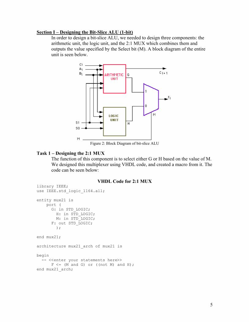
With these equations we created a Full-Adder macro using VHDL code. The screen capture of the code can be seen below:
13
Figure 10: Screen Capture of the VHDL Code for our Full Adder
In order to test that our Full Adder worked correctly we executed a Functional Simulation of the macro in Xilinx. The generated waveform can be seen and analyzed below.
Figure 11: Functional Simulation of a Full Adder
Analysis of this waveform illustrates that the Full Adder we created functions properly. If we look between 20ns and 30ns we will see two changes in G and Cout. Between 20ns and 25ns, C=1, X=Y=0, the expected value according to Table 5 is that G=1 and Cout= 0, because 1+0+0=1 without a carry. This is verified on the simulation above. On the other hand, between 25 and 30ns, C=1, X=1, and Y=0. In this case 1+1+0 = 10 which is 0 and a carry-bit. This is again, proven to be the case in the Functional Simulation above.

14
d. Compiling the Arithmetic Unit
After testing each of the components of our Arithmetic Unit we went back to the Schematic Editor in Xilinx Foundation Software and put all the pieces together. Our schematic is shown below.
Figure 12: Schematic Diagram of Arithmetic Unit
In order to test that the Arithmetic Unit functioned properly, we used Functional Simulation in Xilinx to check our circuit. Our functional simulation can is seen below:
Figure 13: Functional Simulation of Arithmetic Unit
Analysis of the above waveforms illustrates that our Arithmetic Unit actually does function properly. If we look at the first segment in green, between 0 and 20 ns, (000 which is representative of S1, S0, and C, respectively), we can see that as expected, the value A is transferred to G. If we look between 20 and 30 ns, 001, A is transferred and then 1 is added. Hence, as illustrated above, the value of G gains the value of ‘1’ and the carry-out ‘0’, to illustrate A, ‘0’ and ‘1’ being added together.

15
Task 4 - Compiling the 1-bit ALU
After testing our Arithmetic and Logic units we generated macros out of them and were ready to put all the units together with the 2:1 multiplexer designed in part A. A schematic of our 1-bit ALU is shown below:
Figure 14: Schematic Diagram of 1-bit ALU
In order to test that our 1-bit ALU we worked properly, we executed Functional Simulation on the inputs and outputs of the above. The generated waveforms are shown below at times when M=0 (Logic) and M=1 (Arithmetic):
Figure 15a: Functional Simulation of 1-bit ALU in Logic Mode (M=0)

16
Figure 15b: Functional Simulation of 1-bit ALU in Logic Mode (M=1)
Analysis of Figure 15a (M=0) between 0 and 20ns illustrates that our 1-bit ALU logic block works properly. Between these times, S1=S0 = 0, which means that the A and B are ANDed together to return the value of F. Due to the fact that F=1 if and only if A=B=1 during this time frame it is evident that our 1-bit ALU works correctly in Logic Mode. In arithmetic mode (Figure 15b), we know that when S1=S0=C=0 the value of A is transferred to the value of F. If you look between 160ns and 180ns, it is clear that this indeed the case. Hence, because both our Logic and Arithmetic Units and the multiplexer that combines them both works properly, we have successfully designed a 1-bit ALU.
Task 5 – Compiling the 4-bit ALU In order to create a 4-bit ALU, we compiled four 1-bit ALUs and added an overflow detector (V = C3 XOR C4) between the Carry-outs of the third and fourth 1-bit ALUs. Our schematic is illustrated below:

17
Figure 16: Schematic Diagram of 4-bit ALU with Overflow Detector
In order to test that our 4-bit ALU worked correctly we executed a Functional Simulation on the inputs and outputs of our above schematic prior to making it into a macro.
Figure 17a: Functional Simulation of 4-bit ALU with Overflow Detector in Logic Mode (M=0)

18
Figure 17b: Functional Simulation of 4-bit ALU with Overflow Detector in Arithmetic Mode (M=1)
Analysis of the above waveforms, illustrates that just as with our 1-bit ALU, our 4-bit ALU was designed correctly and works properly. Looking at our ALU in Logic Operation (figure 17a), when S1 = S0 = 1 (15-20 ns) our output represents that of the XNOR function which is what is supposed to occur. Hence, our logic works properly. For the Arithmetic operation of our ALU, when S1=0, S0=1, C=0, ABUS3 = 0000, and BBUS=0001, A and B are added together, and returns 0001. This is proof that our ALU operates correctly in arithmetic operation. Successful operation in both modes verifies that our 4-bit ALU works correctly. Our next step was to design the implementation portion of our ALU so it can be tested on a Digilab Board.
Task 6- Designing the Main Decoder
Implementation of our 4-bit ALU requires multiple smaller decoders. In this case we created decoders for the LEDs, the 7-segment display and the sign of the result.
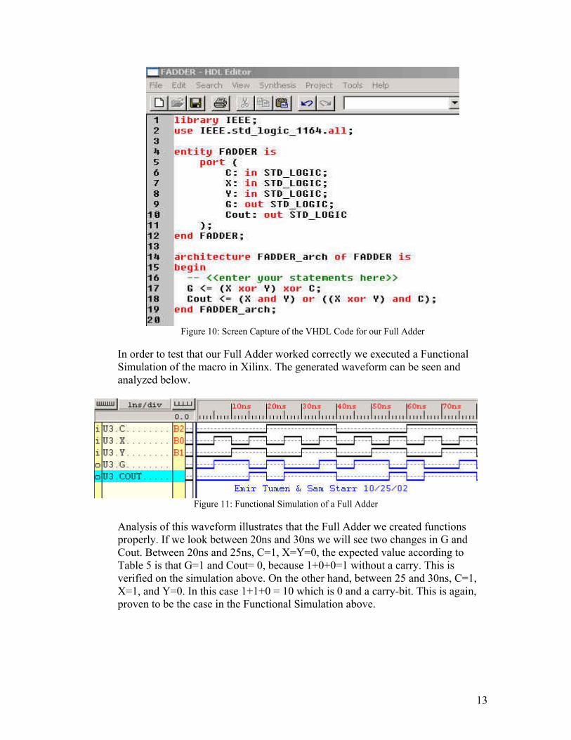
a. Designing the LED Decoder (Logic) Our LED decoder takes the input F and displays its value on an array of LEDs if M=1 after it has been inverted, seen in the schematic of the main decoder (Figure 21). The code and it’s simulated waveform shown below:
VHDL Code for LED Decoder
library IEEE; use IEEE.std_logic_1164.all; entity leddecod is port ( FBUS: in STD_LOGIC_VECTOR (3 downto 0); M: in STD_LOGIC; SIGN: out STD_LOGIC; LEDS: out STD_LOGIC_VECTOR (3 downto 0) ); end leddecod; architecture leddecod_arch of leddecod is
19
signal INPUTS: std_logic_vector (4 downto 0); begin -- <<enter your statements here>> INPUTS(4) <= M; INPUTS(3) <= FBUS(3); INPUTS(2) <= FBUS(2); INPUTS(1) <= FBUS(1); INPUTS(0) <= FBUS(0); with INPUTS select LEDS <= ("0000") when "10000", ("0001") when "10001", ("0010") when "10010", ("0011") when "10011", ("0100") when "10100", ("0101") when "10101", ("0110") when "10110", ("0111") when "10111", ("1000") when "11000", ("1001") when "11001", ("1010") when "11010", ("1011") when "11011", ("1100") when "11100", ("1101") when "11101", ("1110") when "11110", ("1111") when "11111", ("0000") when others; end leddecod_arch;
Figure 18: Functional Simulation of LED Decoder
In each case the LEDs light up accordingly to the output of the FBUS, whenever M=1. Our next step was to design the 7-segment decoder.
b. Designing the 7-Segment Decoder (Arithmetic)
The 7-segment display takes the output value from the ALU Arithmetic operation and displays it on the Digilab board as a digit. The coding for this display and its generated waveform is shown below:
VHDL Code for 7-Segment Display library IEEE; use IEEE.std_logic_1164.all; entity sevensegdec is

20
port ( XBUS: in STD_LOGIC_VECTOR (3 downto 0); Carry: in STD_LOGIC; Error: out STD_LOGIC; TENS: out STD_LOGIC; LEDONE: out STD_LOGIC_VECTOR (6 downto 0) ); end sevensegdec; architecture sevensegdec_arch of sevensegdec is signal INPUTS: std_logic_vector (4 downto 0); begin -- <<enter your statements here>> INPUTS(4) <= Carry; INPUTS(3) <= XBUS(3); INPUTS(2) <= XBUS(2); INPUTS(1) <= XBUS(1); INPUTS(0) <= XBUS(0); with INPUTS select LEDONE <= ("0000001") when "00000", ("1001111") when "00001", ("0010010") when "00010", ("0000110") when "00011", ("1001100") when "00100", ("0100100") when "00101", ("0100000") when "00110", ("0001111") when "00111", ("0000000") when "01000", ("0000100") when "01001", ("0000001") when "01010", ("1001111") when "01011", ("0010010") when "01100", ("0000110") when "01101", ("1001100") when "01110", ("0100100") when "01111", ("0100000") when "10000", ("0001111") when "10001", ("0000000") when "10010", ("1111111") when others; TENS <= Carry or (XBUS(3) and XBUS(2)) or (XBUS(3) and XBUS(1)); Error <= (Carry and XBUS(3)) or (Carry and XBUS(2)) or (Carry and XBUS(1) and XBUS(0)); end sevensegdec_arch;

21
Analysis of this waveform between 5 and 10 ns illustrates proper operation of the seven segment display. When the ALU returns a value of 0001, binary code for the decimal number “1”, the LEDs illuminate in a fashion which displays “1” on the Digilab board. The code it returns “1001111” is the 7-bit code sent to the cathodes of the 7-segment display (hence because it is active-low, illuminating the 2nd and 3rd segments of the display). c. Designing the Sign Decoder
The 7-segment display above, also returns a sign bit as its output. The below code takes this bit, and determines whether to display the negative sign (“1111110”) on the Digilab Board. The code and accompanying waveform are shown below:
Figure 19: Screen Capture of VHDL Code for our Sign Decoder
22
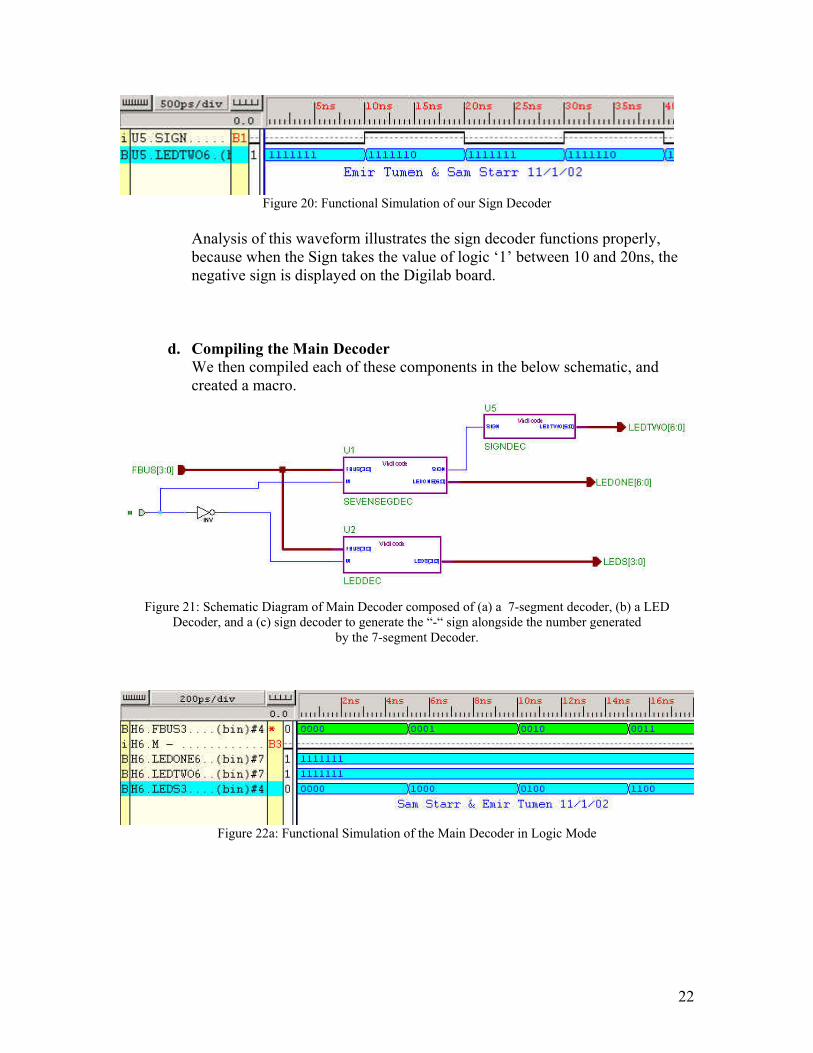
Figure 20: Functional Simulation of our Sign Decoder
Analysis of this waveform illustrates the sign decoder functions properly, because when the Sign takes the value of logic ‘1’ between 10 and 20ns, the negative sign is displayed on the Digilab board.
d. Compiling the Main Decoder We then compiled each of these components in the below schematic, and created a macro.
Figure 21: Schematic Diagram of Main Decoder composed of (a) a 7-segment decoder, (b) a LED
Decoder, and a (c) sign decoder to generate the “-“ sign alongside the number generated by the 7-segment Decoder.
Figure 22a: Functional Simulation of the Main Decoder in Logic Mode

23
Figure 22b: Functional Simulation of the Main Decoder in Arithmetic Mode
In Figure 22a, between 10 and 15ns, the input value from the ALU is 0010, and the output LED form is 0100. It is apparent that if we change the direction of the LED bus, each of the input and output LED values will match, and the LEDs will illuminate according to the input. In Figure 22b, between 40ns and 45ns, the ALU returns a value of 1000, which is the decimal equivalent of ‘-8’. Hence, the sign bus (LEDTWO) displays the negative sign, and the magnitude bus (LEDONE) displays the number 8 on the 7-segment display. Analysis of the above waveform proves that this is the case and our Decoder works properly.
Task 7- Designing the Display Switch Circuit
In order to display both the sign and magnitude values alongside each other, a Display Switch Circuit is needed to flip back and forth between the outputs of LEDONE and LEDTWO. To execute this, the Display Switch Circuit needs to consist of a multiplexer driven by a clock. The value we chose to run the clock on is 490Hz, which is fast enough so that both the sign and magnitude can be seen. The coding for our multiplexer is shown below:
VHDL Code for Display Switch Circuit
library IEEE; use IEEE.std_logic_1164.all; entity MUX is port ( SIGN: in STD_LOGIC_VECTOR (6 downto 0); DSP: in STD_LOGIC_VECTOR (6 downto 0); D: out STD_LOGIC_VECTOR (6 downto 0); S: in STD_LOGIC ); end MUX; architecture MUX_arch of MUX is begin PRO: process (SEQ, DSP, S) begin if (S = '1') then D <= SIGN; else D <= DSP;
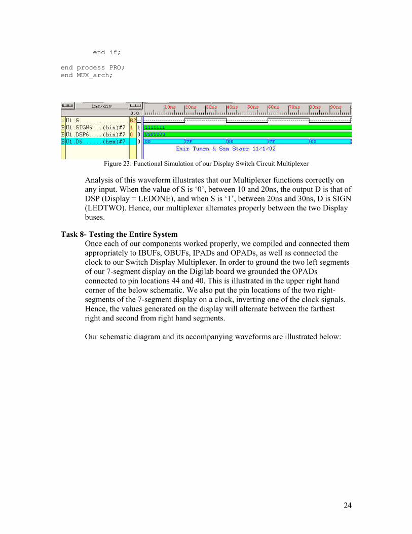
24
end if; end process PRO; end MUX_arch;
Figure 23: Functional Simulation of our Display Switch Circuit Multiplexer
Analysis of this waveform illustrates that our Multiplexer functions correctly on any input. When the value of S is ‘0’, between 10 and 20ns, the output D is that of DSP (Display = LEDONE), and when S is ‘1’, between 20ns and 30ns, D is SIGN (LEDTWO). Hence, our multiplexer alternates properly between the two Display buses.
Task 8- Testing the Entire System
Once each of our components worked properly, we compiled and connected them appropriately to IBUFs, OBUFs, IPADs and OPADs, as well as connected the clock to our Switch Display Multiplexer. In order to ground the two left segments of our 7-segment display on the Digilab board we grounded the OPADs connected to pin locations 44 and 40. This is illustrated in the upper right hand corner of the below schematic. We also put the pin locations of the two right-segments of the 7-segment display on a clock, inverting one of the clock signals. Hence, the values generated on the display will alternate between the farthest right and second from right hand segments. Our schematic diagram and its accompanying waveforms are illustrated below:

25
Figure 24: Schematic Diagram of Entire 4-bit ALU System
Figure 25a: Functional Simulation in Logic Mode
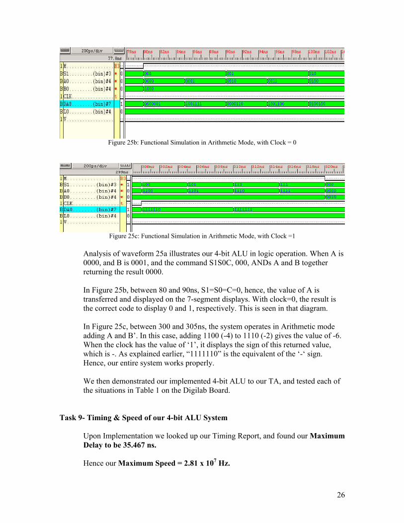
26
Figure 25b: Functional Simulation in Arithmetic Mode, with Clock = 0
Figure 25c: Functional Simulation in Arithmetic Mode, with Clock =1
Analysis of waveform 25a illustrates our 4-bit ALU in logic operation. When A is 0000, and B is 0001, and the command S1S0C, 000, ANDs A and B together returning the result 0000. In Figure 25b, between 80 and 90ns, S1=S0=C=0, hence, the value of A is transferred and displayed on the 7-segment displays. With clock=0, the result is the correct code to display 0 and 1, respectively. This is seen in that diagram. In Figure 25c, between 300 and 305ns, the system operates in Arithmetic mode adding A and B’. In this case, adding 1100 (-4) to 1110 (-2) gives the value of -6. When the clock has the value of ‘1’, it displays the sign of this returned value, which is -. As explained earlier, “1111110” is the equivalent of the ‘-‘ sign. Hence, our entire system works properly. We then demonstrated our implemented 4-bit ALU to our TA, and tested each of the situations in Table 1 on the Digilab Board.
Task 9- Timing & Speed of our 4-bit ALU System
Upon Implementation we looked up our Timing Report, and found our Maximum Delay to be 35.467 ns. Hence our Maximum Speed = 2.81 x 10⁷ Hz.

27
Conclusion
In conclusion, our 4-bit ALU design and implementation worked correctly. The methods we used to design each component in the system made for proper execution of the ALU. While at first we had issues turning off the required 7-segment displays, and switching between them. Once we figured this out, the project worked correctly. This lab let us use the knowledge we have gained over the past labs, to design a given project. We also kept in mind making our project as time efficient as possible.
Signatures: _____________________________ ______________________________ Your Name Partner's name