Embed Size (px)
Citation preview

I/O Control Hub 2, 3, and 4 EEPROM Map and Programming InformationApplication Note (AP-409)
Revision 2.2December 2004

Application Note (AP-409)
Information in this document is provided in connection with Intel products. No license, express or implied, by estoppel or otherwise, to any intellectual property rights is granted by this document. Except as provided in Intel's Terms and Conditions of Sale for such products, Intel assumes no liability whatsoever, and Intel disclaims any express or implied warranty, relating to sale and/or use of Intel products including liability or warranties relating to fitness for a particular purpose, merchantability, or infringement of any patent, copyright or other intellectual property right. Intel products are not intended for use in medical, life saving, or life sustaining applications.
Intel may make changes to specifications and product descriptions at any time, without notice.
Designers must not rely on the absence or characteristics of any features or instructions marked "reserved" or "undefined." Intel reserves these for future definition and shall have no responsibility whatsoever for conflicts or incompatibilities arising from future changes to them.
The I/O Control Hub 2, 3, and 4 may contain design defects or errors known as errata which may cause the product to deviate from published specifications. Current characterized errata are available on request.
Contact your local Intel sales office or your distributor to obtain the latest specifications and before placing your product order.
Copies of documents which have an ordering number and are referenced in this document, or other Intel literature may be obtained by calling 1-800-548-4725 or by visiting Intel's Web site at http://www.intel.com.
Copyright © 2004, Intel Corporation. All rights reserved.
* Other product and corporate names may be trademarks of other companies and are used only for explanation and to the owners’ benefit without intent to infringe.
I/O Control Hub 2, 3, and 4
Contents1.0 Introduction and Scope ......................................................................................................1
1.1 EEPROM Device and Interface....................................................................................11.2 EEPROM Programming Procedure Overview .............................................................21.3 ICH2, ICH3, and ICH4 EEPROM Utility .......................................................................2
2.0 ICH2, ICH3, and ICH4 EEPROM Format and Contents ....................................................22.1 Ethernet Individual Address .........................................................................................42.2 Compatibility Fields ......................................................................................................4
2.2.1 Compatibility Byte 0 ..............................................................................................42.2.2 Compatibility Byte 1 ..............................................................................................5
2.3 ICH2, ICH3, and ICH4 Hardware Description Fields ...................................................62.3.1 Controller Type ......................................................................................................62.3.2 Connector Types ...................................................................................................72.3.3 PHY Device Records .............................................................................................72.3.4 Printed Wire Assembly Number.............................................................................9
2.4 ICH2, ICH3, and ICH4 Product Identification ...............................................................92.4.1 EEPROM ID...........................................................................................................92.4.2 ICH2 Integrated 10/100 Mbps LAN Controller Product Identification ..................112.4.3 ICH3 Integrated 10/100 Mbps LAN Controller Product Identification ..................142.4.4 ICH4 Integrated 10/100 Mbps LAN Controller Product Identification ..................16
2.5 Integrated Alert on LAN Information...........................................................................182.5.1 SMB Address and Heartbeat Packet Pointer.......................................................182.5.2 Heartbeat Packet Structure within the EEPROM.................................................18
2.6 Boot Agent Configuration Information ........................................................................202.6.1 Boot Agent Main Setup Options (Word 30h) .......................................................202.6.2 Boot Agent Configuration Customization Options (Word 31h) ............................232.6.3 Boot Agent Configuration Customization Options (Word 32h) ............................242.6.4 IBA Capabilities (Word 33h) ................................................................................25
2.7 Checksum ..................................................................................................................25
AppendicesA ICH2 EEPROM Contents .................................................................................................27
B ICH3 EEPROM Contents .................................................................................................31
C ICH4 EEPROM Contents .................................................................................................37
Figures1 Heartbeat Packet Example...............................................................................................19
Application Note (AP-409) iii
I/O Control Hub 2, 3, and 4
Tables1 ICH2, ICH3, and ICH4 EEPROM Address Map ...........................................................................22 Ethernet Individual Address Words 00h to 02h ............................................................................ 43 Controller Type IDs....................................................................................................................... 64 PHY Device Codes....................................................................................................................... 85 ICH2, ICH3, and ICH4 EEPROM Word Ah .................................................................................. 96 Product Names/Configurations/IDs for ICH3.............................................................................. 157 Product Names/Configurations IDs for ICH4.............................................................................. 178 Boot Agent Main Setup Options ................................................................................................. 209 Boot Agent Configuration Customization Options (Word 31h) .................................................. 2310 Boot Agent Configuration Customization Options (Word 32h) .................................................. 2411 IBA Capabilities ......................................................................................................................... 2512 ICH2 EEPROM Contents ........................................................................................................... 2713 ICH3 EEPROM Contents ........................................................................................................... 3114 ICH4 EEPROM Contents ........................................................................................................... 37
Revision History
Revision Revision Date Description
0.7 Feb. 2000 Initial release (Intel Secret).
0.9 May 2000 Intel Secret.• Modified table in Section 2.4.2, ”ICH2 Integrated 10/100 Mbps LAN Control-
ler Product Identification” to reflect new Revision ID number.• Revised table in Section 2.4.2.1, ”Subsystem ID” to include adapter and LAN
on Motherboard (LOM) product configurations.• Modified Table 10 and Table 11in Section 2.6.1, “Boot Configuration”.
1.3 Apr. 2001 Intel Secret.Added information for I/O Control Hub 3.
1.7 Jun. 2001 Intel Secret.• Clarified description of Alternate Revision ID field in Section 2.4.1,
”EEPROM ID”, Table 5.• Clarified description of word 31h in Section 2.6.1.2, “Boot Configuration
Word 31h”.
1.8 Nov 2001 Intel Secret. Added ICH4 Info. Changed to Anacapa number system.
1.9 Jan 2002 Added ICH5 Info
2.0 May 2003 Modified Table 1, Sections 2.21, 2.51, D2, D3, D4
2.01 Jan 2004 Changed document status to non-confidential.
2.1 July 2004 Added information for I/O Control Hub 6 (ICH6).
2.2 Dec 2004 • Removed I/O Control Hub (ICH5 and ICH6) information.• Updated Boot Agent information to reflect the latest version.• Removed 82562EH and HPNA references.• Removed references to 82557 and 82558 devices.
iv Application Note (AP-409)

I/O Control Hub 2, 3, and 4
1.0 Introduction and Scope
The scope of this application note describes the EEPROM and its contents for products based upon the Intel® I/O Control Hub 2 (ICH2), I/O Control Hub 3 (ICH3), and I/O Control Hub 4 (ICH4) devices. These components include an integrated 10/100 Mbps LAN controller.
The EEPROM is used for hardware and software configuration. It is read by software to determine and configure specific design features. For compatibility, Intel does not create separate drivers for the integrated ICH2, ICH3, and ICH4 controllers.
Unless otherwise specified, all numbers in this document use the following numbering convention:
• Numbers that do not have a suffix are decimal (base 10).
• Numbers with a suffix of “h” are hexadecimal (base 16).
• Numbers with a suffix of “b” are binary (base 2).
1.1 EEPROM Device and Interface
The serial EEPROM stores configuration data for the controller and is an input and output device. The ICH2, ICH3, and ICH4 support 64-word or 256-word sized EEPROMs.
82562EZ/ET based designs require a 64-word EEPROM. A 256-word EEPROM device is required in 82562EM, 82562EP or 82562EX based systems to store the heartbeat packet.
All accesses, read and write, are preceded by a command instruction to the EEPROM. The command instructions begin with a logical one as a start bit, two opcode bits (read, write, erase, etc.), and six address bits. The end of the address field is indicated by a dummy zero bit from the EEPROM. This indicates that the entire address field has been transferred to the EEPROM. A command is issued by asserting the EEPROM Chip Select signal from the controller and clocking the data out of the EEPROM Data Input signal (which is the EEPROM Data Output signal from the ICH2, ICH3, and ICH4 controller perspective) into the EEPROM on its data input pin relative to the EEPROM Shift Clock controller output. The EEPROM Chip Select signal is de-asserted after the EEPROM cycle completes (command, address and data).
The ICH2, ICH3, and ICH4 automatically read the EEPROM after power-up to retrieve configuration information. The length of an EEPROM read is approximately 12,480 clock cycles (499.2 microseconds at 100 Mbps LAN connection or 5.0 milliseconds at 10 Mbps LAN connection). Designs using a 256-word EEPROM have an EEPROM read length of approximately 15,296 clock cycles long (611.8 microseconds at 100 Mbps LAN connection or 6.1 milliseconds at 10 Mbps LAN connection).
Application Note (AP-409) 1

I/O Control Hub 2, 3, and 4
1.2 EEPROM Programming Procedure Overview
The EEPROM can be programmed on-board through the ICH2, ICH3, and ICH4. This enables the use of a surface mount technology (SMT) EEPROM, which is otherwise difficult to handle with off-line automated programming equipment. The bill of materials (BOM) for an ICH2, ICH3, and ICH4 based solution requires a blank EEPROM (93C66 for 82562EP/EM or 82562EX systems, and 93C46 for 82562EZ/ET systems). Prior to programming the EEPROM, a data file unique to the Printed Board Assembly (PBA) is required. The data file contains the default EEPROM values for that particular PBA. The EEPROM image contains static and dynamic data. Static data is the basic platform configuration information. Dynamic data holds the product’s Ethernet Individual Address (IA) and EEPROM checksum. This file can be created in a simple text editor and follows the format shown in the Appendices, which provides an example of an EEPROM map for an ICH2, ICH3, and ICH4 based designs.
EEPROMs may be programmed prior to board soldering. Some designers may prefer this method over inline programming.
1.3 ICH2, ICH3, and ICH4 EEPROM Utility
Intel has created a DOS utility to meet the two basic requirements for in-circuit programming:
• Update EEPROM images. This utility can be used to update EEPROM images as part of an end-of-line production tool.
• Used as a stand-alone development tool. This tool uses two basic data files (static data file and IA address file) as described in following sections.
The ICH2, ICH3, and ICH4 EEPROM utility is flexible and can be used to update the entire EEPROM image or update only the IA address of the card. This utility is only available to OEM customers.
2.0 ICH2, ICH3, and ICH4 EEPROM Format and Contents
Table 1 lists the EEPROM map for the ICH2, ICH3, and ICH4. Each word listed is described in detail in following sections.
Table 1. ICH2, ICH3, and ICH4 EEPROM Address Map
Word HIgh Byte (Bits 15:8) Low Byte (Bits 7:0) Used by
00h Ethernet Individual Address Byte 2 Ethernet Individual Address Byte 1 Hardware
01h Ethernet Individual Address Byte 4 Ethernet Individual Address Byte 3 Hardware
02h Ethernet Individual Address Byte 6 Ethernet Individual Address Byte 5 Hardware
03h Compatibility Byte 1 Compatibility Byte 0 Intel® driver
04h Reserved
05h Controller Type (02h for ICH2, ICH3, and ICH4) Connector Type Intel® driver
06h PHY Device Record
2 Application Note (AP-409)

I/O Control Hub 2, 3, and 4
Words 00h through 02h are used by the hardware and are common to all controllers. If the value inword 23h is not 0000h or FFFFh, the ICH3, and ICH4 Device ID uses the information in this word.
Caution: OEMs must ensure that word 40h in the EEPROM image is set to 0x0044 (not 0xFFFF). Word 40h contains pointers for the internal micro-machine, and an incorrect setting will lockup the controller. This condition applies to the 82562EP, 82562EM and 82562EX devices (Basic Alerting).
07h Reserved
08h PWA Number Byte 4 PWA Number Byte 3 Factory
09h PWA Number Byte 2 PWA Number Byte 1 Factory
0Ah EEPROM ID Hardware
0Bh Subsystem ID Hardware
0Ch Subsystem Vendor ID Hardware
0Dh AoL Config Heartbeat Packet Pointer SMB Address Field
Alert on LAN driver and hardware
0Eh to 22h Reserved
23hICH2 = ReservedICH3 = Device IDICH4 = Device ID
24h to 2Fh Reserved
30h to 33h Intel Boot Agent Configuration Firmware
34h to 3Fh Reserved
40h to FAh Alert on LAN alert packet structure Alert on LAN
driver
FFh Checksum Driver
Table 1. ICH2, ICH3, and ICH4 EEPROM Address Map
Word HIgh Byte (Bits 15:8) Low Byte (Bits 7:0) Used by
Application Note (AP-409) 3

I/O Control Hub 2, 3, and 4
2.1 Ethernet Individual Address
The Ethernet Individual Address (IA) is a six byte field that must be unique for each adapter card or board and unique for each copy of the EEPROM image. The first three bytes are vendor-specific. The last three bytes must be unique for each copy of the EEPROM. OEM versions of the product may be required to have non-Intel ID’s in the first three byte positions. The Intel default is shown in Table 2.
Note: The Ethernet IA is byte swapped, as indicated in Table 2.
Note: The IA bytes read from the EEPROM are used by ICH2, ICH3, and ICH4 until an IA Setup command is issued by software. The IA defined by the IA Setup command overrides the IA read from the EEPROM.
2.2 Compatibility Fields
The compatibility fields are used by Intel drivers to determine software compatibility. Only one word in the EEPROM image is reserved for compatibility information. New bits within these fields will be defined as the need arises for determining software compatibility between various hardware revisions. These bytes are initialized during manufacturing and should be considered read only by software.
2.2.1 Compatibility Byte 0
Table 2. Ethernet Individual Address Words 00h to 02h
Individual Address Byte
Word 00 Word 01 Word 02
Manufacturer MAC Address Byte 1 Byte 0 Byte 1 Byte 0 Byte 1 Byte 0
Intel 00AA00XXYYZZh AAh 00h XXh 00h ZZh YYh
Intel 00A0C9XXYYZZh A0h 00h XXh C9h ZZh YYh
Intel 009027XXYYZZh 90h 00h XXh 27h ZZh YYh
D7 D6 D5 D4 D3 D2 D1 D0
RFU (0b)
RFU (0b)
RFU (0B) SMB
Alert on LAN 2 (0b)
BOB (0B)
MC100 (1b)
MC10 (1b)
Bit Name Description
7:5 RFU Reserved for future use. These bits should be set to 000b.
4 SMB
System Management Bus to Motherboard Connection. This bit indicates whether the Ethernet controller's System Management Bus (SMbus) is connected to the motherboard, thereby enabling alerting capability within the ICH2, ICH3, and CH4. It is set as follows:• 0b for the 82562ET/82562EZ• 1b for the 82562EM, 82562EP or 82562EM/EP/EX.
4 Application Note (AP-409)

I/O Control Hub 2, 3, and 4
2.2.2 Compatibility Byte 1
Bit Name Description
3 Alert on LAN 2
Alert on LAN 2 ASIC Present. .For the ICH2, ICH3 and ICH4 this bit indicates whether or not an Alert on LAN 2 ASIC is present and connected to the main SMBus.1b = Alert on LAN 2 ASIC is connected to the controller's SMBus.0b = Alert on LAN 2 ASIC is not connected to the controller's SMBus.This bit was specifically added for 82559 designs using the Alert on LAN 2 ASIC.This bit is set to 0b when using the ICH2, ICH3, and ICH4 with any 82562 device.
2 BOB
Bridge On Board. The BOB bit allows software to determine whether an adaptor has a PCI bridge without scanning the PCI bus and without relying on using the Subsystem ID. It is necessary since software is not always allowed to scan the PCI bus during configuration and because OEMs are allowed to change the value of the Subsystem ID.1b = Network Interface Card has a PCI bridge.0b = Network Interface Card does not have a PCI bridge.This bit is set to 0b in the ICH2, ICH3, and ICH4 devices.
1 MC100
Multicast Workaround 100 Mbps. The MC100 bit is discussed in further detail in the 8255X EEPROM Map and Programming Information Application Note (AP-394).This bit is set to 1b in the ICH2, ICH3, and ICH4 devices.
0 MC10
Multicast Workaround 10 Mbps. The MC10 bit is discussed in further detail in the 8255X EEPROM Map and Programming Information Application Note (AP-394).This bit is set to 1b in ICH2, ICH3, and ICH4 devices.
D7 D6 D5 D4 D3 D2 D1 D0
RFU (0b)
RFU (0b)
RFU (0b)
ICH2/ICH3/ICH4(1b)
LOM (1b)
SRV (0b) CLI (1b) OEM
Bit Name Description
7:5 RFU Reserved for future use. These bits should be set to 000b.
4 ICH2/ICH3/ICH4
ICH2/ICH3/ICH4. This bit indicates to software that this design uses an ICH2, ICH3, or ICH4 controller.1b = An ICH2, ICH3, or ICH4 controller is located on the motherboard.0b = An ICH2, ICH3, or ICH4 controller is not on the motherboard.This bit is set to 1b for ICH2, ICH3, and ICH4.
3 LOM
ICH2/ICH3/ICH4 Integrated with LAN on Motherboard. This bit indicates to software that the ICH2, ICH3, or ICH4 device is located on the motherboard.This bit is set to 1b for ICH2, ICH3, and ICH4.
Application Note (AP-409) 5
I/O Control Hub 2, 3, and 4
NOTE: If the CLI bit equals 0b, the adapter should be considered a legacy product and the feature set is undefined.
2.3 ICH2, ICH3, and ICH4 Hardware Description Fields
The hardware description fields of the EEPROM describe the component configuration for the product (design). These fields are used by Intel drivers and the controller to determine ICH2, ICH3, and ICH4 with integrated LAN controller configuration.
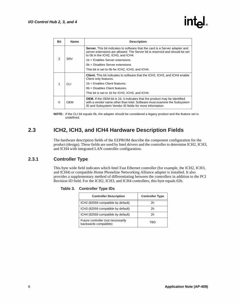
2.3.1 Controller Type
This byte wide field indicates which Intel Fast Ethernet controller (for example, the ICH2, ICH3, and ICH4) or compatible Home Phoneline Networking Alliance adapter is installed. It also provides a supplementary method of differentiating between the controllers in addition to the PCI Revision ID field. For the ICH2, ICH3, and ICH4 controllers, this byte equals 02h.
Bit Name Description
2 SRV
Server. This bit indicates to software that the card is a Server adapter and server extensions are allowed. The Server bit is reserved and should be set to 0b in the ICH2, ICH3, and ICH4.1b = Enables Server extensions.0b = Disables Server extensions.This bit is set to 0b for ICH2, ICH3, and ICH4.
1 CLI
Client. This bit indicates to software that the ICH2, ICH3, and ICH4 enable Client only features.1b = Enables Client features.0b = Disables Client features.This bit is set to 1b for ICH2, ICH3, and ICH4.
0 OEMOEM. If the OEM bit is 1b, it indicates that the product may be identified with a vendor name other than Intel. Software must examine the Subsystem ID and Subsystem Vendor ID fields for more information.
Table 3. Controller Type IDs
Controller Description Controller Type
ICH2 (82559 compatible by default) 2h
ICH3 (82559 compatible by default) 2h
ICH4 (82559 compatible by default) 2h
Future controller (not necessarily backwards compatible) TBD
6 Application Note (AP-409)

I/O Control Hub 2, 3, and 4
2.3.2 Connector Types
This word identifies the connector types used in the design. An RJ-45 connector is used for an Ethernet controller. Its type equals 01h.
2.3.3 PHY Device Records
The PHY device records are used to describe an external PHY. In ICH2, ICH3, and ICH4 based designs, word 07h is not used. Word 06h contains a value of 4701h for the 82562ET, 82562EM or 82562EP. Word 07h should equal 0000h.
D7 D6 D5 D4 D3 D2 D1 D0
RFU (0b)
RFU (0b)
RFU (0b) RJ-11 MII (0b) AUI (0b) BNC
(0b) RJ-45
Bit Name Description
7:5 RFU Reserved for future use. These bits should be set to 000b.
4 RJ-11RJ-11. The RJ-11 bit identifies whether an RJ-11 connector is installed.0b = 82562ET, 82562EM, or 82562EP, 82562EZ or 82562EX.
3 MII
MII. The MII bit indicates whether 10BASE-T and 100BASE-T is supported through an external transceiver. The MII Status Register specifies which 100BASE-T technology is provided (for example, TX or T4).
2 AUI AUI. The AUI bit indicates whether 10BASE-5 technology is supported.
1 BNC BNC. The BNC bit indicates whether 10BASE-2 technology is supported.
0 RJ-45
RJ-45. The RJ-45 bit identifies whether an RJ-45 connector is installed. The ICH2, ICH3, and ICH4 supports 10BASE-T and 100BASE-T technology. The MII Status Register specifies which 100BASE-T technology is provided (for example, TX or T4). The 82562ET, 82562EM, 82562EP, 82562EZ and 82562EX use an RJ-45 connector.1b = 82562ET, 82562EM, 82562EP, 82562EZ or 82562EX.
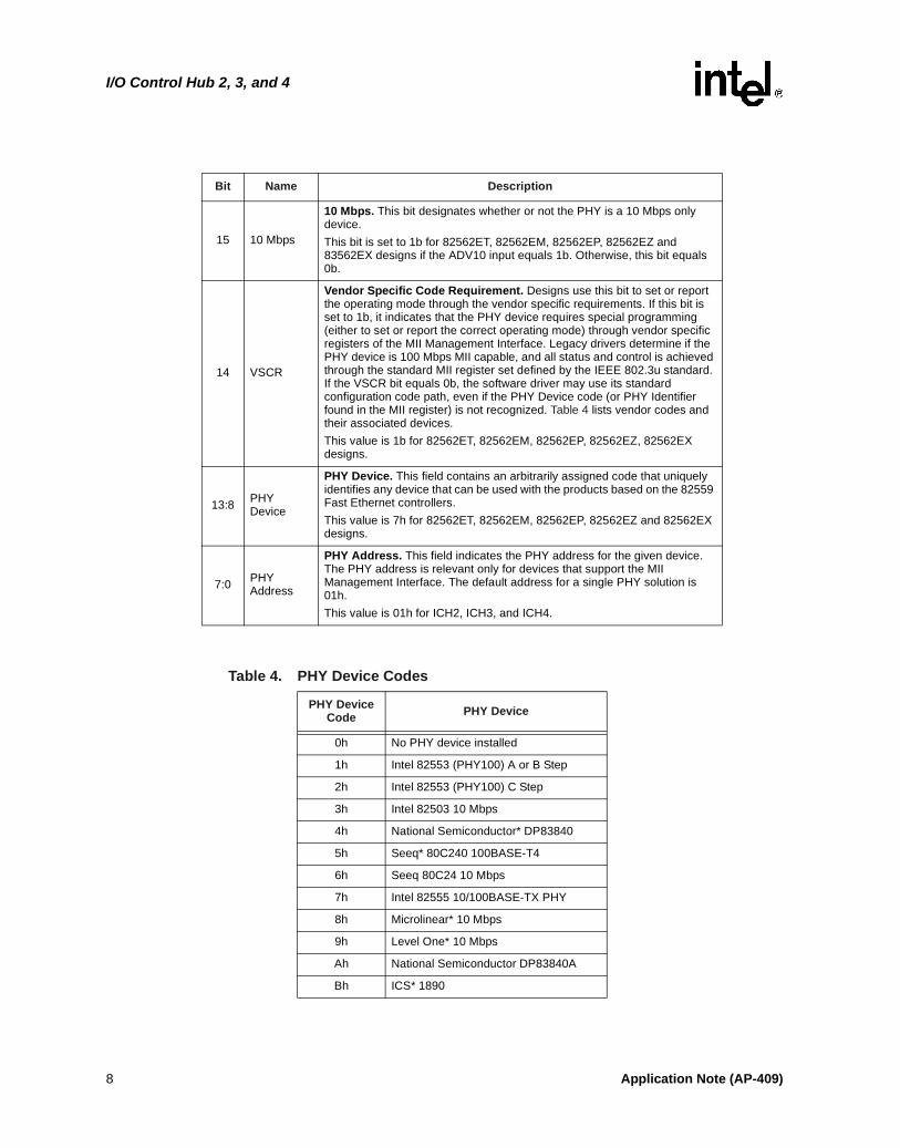
D15 D14 D13 - D8 D7 - D0
10 Mbps VSCR PHY Device PHY Address
Application Note (AP-409) 7
I/O Control Hub 2, 3, and 4
Bit Name Description
15 10 Mbps
10 Mbps. This bit designates whether or not the PHY is a 10 Mbps only device.This bit is set to 1b for 82562ET, 82562EM, 82562EP, 82562EZ and 83562EX designs if the ADV10 input equals 1b. Otherwise, this bit equals 0b.
14 VSCR
Vendor Specific Code Requirement. Designs use this bit to set or report the operating mode through the vendor specific requirements. If this bit is set to 1b, it indicates that the PHY device requires special programming (either to set or report the correct operating mode) through vendor specific registers of the MII Management Interface. Legacy drivers determine if the PHY device is 100 Mbps MII capable, and all status and control is achieved through the standard MII register set defined by the IEEE 802.3u standard. If the VSCR bit equals 0b, the software driver may use its standard configuration code path, even if the PHY Device code (or PHY Identifier found in the MII register) is not recognized. Table 4 lists vendor codes and their associated devices.This value is 1b for 82562ET, 82562EM, 82562EP, 82562EZ, 82562EX designs.
13:8 PHY Device
PHY Device. This field contains an arbitrarily assigned code that uniquely identifies any device that can be used with the products based on the 82559 Fast Ethernet controllers.This value is 7h for 82562ET, 82562EM, 82562EP, 82562EZ and 82562EX designs.
7:0 PHY Address
PHY Address. This field indicates the PHY address for the given device. The PHY address is relevant only for devices that support the MII Management Interface. The default address for a single PHY solution is 01h.This value is 01h for ICH2, ICH3, and ICH4.
Table 4. PHY Device Codes
PHY Device Code PHY Device
0h No PHY device installed
1h Intel 82553 (PHY100) A or B Step
2h Intel 82553 (PHY100) C Step
3h Intel 82503 10 Mbps
4h National Semiconductor* DP83840
5h Seeq* 80C240 100BASE-T4
6h Seeq 80C24 10 Mbps
7h Intel 82555 10/100BASE-TX PHY
8h Microlinear* 10 Mbps
9h Level One* 10 Mbps
Ah National Semiconductor DP83840A
Bh ICS* 1890
8 Application Note (AP-409)
I/O Control Hub 2, 3, and 4
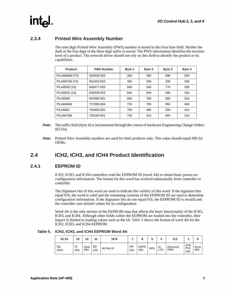
2.3.4 Printed Wire Assembly Number
The nine digit Printed Wire Assembly (PWA) number is stored in this four byte field. Neither the dash or the first digit of the three digit suffix is stored. The PWA information identifies the revision level of a product. The network driver should not rely on this field to identify the product or its capabilities.
Note: The suffix field (byte 4) is incremented through the course of hardware Engineering Change Orders (ECOs).
Note: Printed Wire Assembly numbers are used for Intel products only. This value should equal 00h for OEMs.
2.4 ICH2, ICH3, and ICH4 Product Identification
2.4.1 EEPROM ID
ICH2, ICH3, and ICH4 controllers read the EEPROM ID (word Ah) to obtain basic power-on configuration information. The format for this word has evolved substantially from controller to controller.
The Signature bits of this word are used to indicate the validity of this word. If the signature bits equal 01b, the word is valid and the remaining contents of the EEPROM ID are used to determine configuration information. If the Signature bits do not equal 01b, the EEPROM ID is invalid and the controller uses default values for its configuration.
Word Ah is the only section of the EEPROM map that affects the basic functionality of the ICH2, ICH3, and ICH4. Although other fields within the EEPROM are loaded into the controller, their impact is limited to loading values such as the IA. Table 5 shows the format of word Ah for the ICH2, ICH3, and ICH4 EEPROM.
Product PWA Number Byte 1 Byte 2 Byte 3 Byte 4
PILA8465B (TX) 352509-003 35h 25h 09h 03h
PILA8475B (T4) 352433-003 35h 24h 33h 03h
PILA8500 (10) 645477-003 64h 54h 77h 03h
PILA8520 (10) 649439-003 64h 94h 39h 03h
PILA8460 697680-001 69h 76h 80h 01h
PILA8460B 727095-004 72h 70h 95h 04h
PILA8461 704920-001 70h 49h 20h 01h
PILA8470B 735190-001 73h 51h 90h 01h
Table 5. ICH2, ICH3, and ICH4 EEPROM Word Ah
15:14 13 12 11 10:8 7 6 5 4 3:2 1 0
Sig(01b)
ID(0b)
Rsvd (0b)
BD(1b) Alt Rev ID PM
(1b)DDPD(0b) WOL IA
LEDReserved (00b)
STB Ena(1b)
Rsvd (0b)
Application Note (AP-409) 9

I/O Control Hub 2, 3, and 4
Bits Name Description
15:14 Sig
Signature. If the SIG field equals 01b, the remainder of word Ah is read to determine the basic functionality of the ICH2, ICH3, and ICH4. If the SIG field does not contain a value of 01b, then the remainder of word Ah is ignored and default configuration values are used for the parameters that would have been configured by this word.These bits are 01b for ICH2, ICH3, and ICH4.
13 ID
ID. The ID bit indicates how the Subsystem ID and Subsystem Vendor ID will be used. If the controller detects the presence of an EEPROM (as indicated by a value of 01b in the Signature field) and bit 13 is set (1b), then the Device ID and Vendor ID fields are loaded as follows:• ICH2. The value stored in word Bh (Subsystem ID) is loaded into the Device ID field,
and the Vendor ID field is loaded from word Ch (Subsystem Vendor ID).• ICH3/ICH4. The value stored in word 23h (Device ID) is loaded into the Device ID,
and the Vendor ID field is loaded from word Ch (Vendor ID).If bit 13 is clear (0b), then the Device ID and Vendor ID fields in PCI Configuration space remain at their default values.This bit is set to 0b for ICH2, ICH3, and ICH4.
12 RsvdReserved. This bit is reserved and should be set to 0b. This bit cannot be reassigned to any other function.This bit is set to 0b for ICH2, ICH3, and ICH4.
11 BDBoot Disable. The Boot Disable bit disables the Expansion ROM Base Address Register (PCI Configuration space, offset 30h) when it is set.This bit is set to 1b for ICH2, ICH3, and ICH4.
10:8 Alt Rev ID
Alternate Revision ID. These three bits are used as the three least significant bits of the device revision if bits 15:14 equal 01b and the PCI Revision ID is set as described in:Section 2.4.2, "ICH2 Integrated 10/100 Mbps LAN Controller Product Identification",Section 2.4.3, "ICH3 Integrated 10/100 Mbps LAN Controller Product Identification",Section 2.4.4, "ICH4 Integrated 10/100 Mbps LAN Controller Product Identification",For the ICH2, ICH3, and ICH4, these bits should be set to mirror the Revision ID of the silicon.Note: In most cases, the Alternate Revision ID is not used. However, these bits should mirror the revision of the silicon in the event this field is unintentionally enabled.
7 PM Power Management. The PM bit should always be set to 1b (always enabled) for the ICH2, ICH3, and ICH4.
6 DDPD
Disable Deep Power Down. 0b = Deep Power Down enabled in the D3 state while Power Management is disabled.1b = Deep Power Down disabled in the D3 state while Power Management is disabled.When using the Intel® Alert on LAN Software Development Kit (SDK), this bit is controlled by the Alert on LAN software as the system transitions through power states.This bit is set to 0b for ICH2, ICH3, and ICH4.
10 Application Note (AP-409)

I/O Control Hub 2, 3, and 4
2.4.2 ICH2 Integrated 10/100 Mbps LAN Controller Product Identification
To support OEM branded products, the following optional fields provide additional information for the identification of the vendor and product. These optional fields have been implemented if they contain a value other than 0000h or FFFFh.
The ICH2 with integrated 10/100 Mbps LAN implements the Subsystem ID and Subsystem Vendor ID fields and reads the information from these locations in the EEPROM and uses it according to the PCI Specification, Revision 2.1.
The Subsystem Vendor ID field identifies the vendor of an ICH2 based solution. The Subsystem Vendor ID values are based upon the vendor’s PCI Vendor ID and are controlled by the PCI Special Interest Group (SIG).
The Subsystem ID field identifies the ICH2 based specific solution implemented by the vendor indicated in the Subsystem Vendor ID field.
The ICH2 provides support for configurable Subsystem Vendor ID and Subsystem ID fields for the embedded LAN function. After hardware reset is de-asserted, the ICH2 automatically reads EEPROM words Ah through Ch. The first of these 16 bit values is used for controlling various
5 WOL
Wake on LAN. 0b = WOL mode disabled.1b = WOL mode enabled.If the Wake on LAN (WOL) bit is set and Wake on Magic Packet* or Wake on Link Status Change are enabled, the Power Management Enable (PME) bit is ignored with respect to these events. In this case, the Power Management Event signal should be asserted by Magic Packet Wake or Link Status Change.The WOL bit is set to put the ICH2, ICH3, and ICH4 into Wake on LAN mode. These devices enter WOL mode after the Power-up Reset signal is asserted and they have read the EEPROM. When the ICH2, ICH3, and ICH4 are in WOL mode, the devices read three additional words from the EEPROM (words 0h, 1h, and 2h). These words are expected to contain the Individual Address.This bit is configured by the OEM.
4 IA LED
Individual Address LED. This bit controls the Activity LED (ACTLED) functionality in Wake on LAN (WOL) mode.0b = In WOL mode, the ACTLED is activated by the transmission and reception of broadcast and Individual Address match packets.1b = In WOL mode, the ACTLED is activated by the transmission and reception of Individual Address match packets only.This bit is configured by the OEM.
3:2 Reserved Reserved. These bits are reserved and should be set to 00b. These bits cannot be reassigned to any other function.
1 STB Enable
Standby Enable. The Standby Enable bit enables the ICH2, ICH3, and ICH4 to enter standby mode. When this bit equals 1b, the ICH2, ICH3, and ICH4 can recognize an idle state and can enter standby mode (some internal clocks are stopped for lower power consumption). They do not require a PCI clock signal in standby mode. If this bit equals 0b, the idle recognition circuit is disabled and the ICH2, ICH3, and ICH4 will always remain in an active state. Thus, these devices always request the PCI clock signal using the Clockrun mechanism.This bit is set to 1b for ICH2, ICH3, and ICH4.
0 Rsvd Reserved. This bit is reserved and should be set to 0b. This bit cannot be reassigned to any other function.
Bits Name Description
Application Note (AP-409) 11
I/O Control Hub 2, 3, and 4
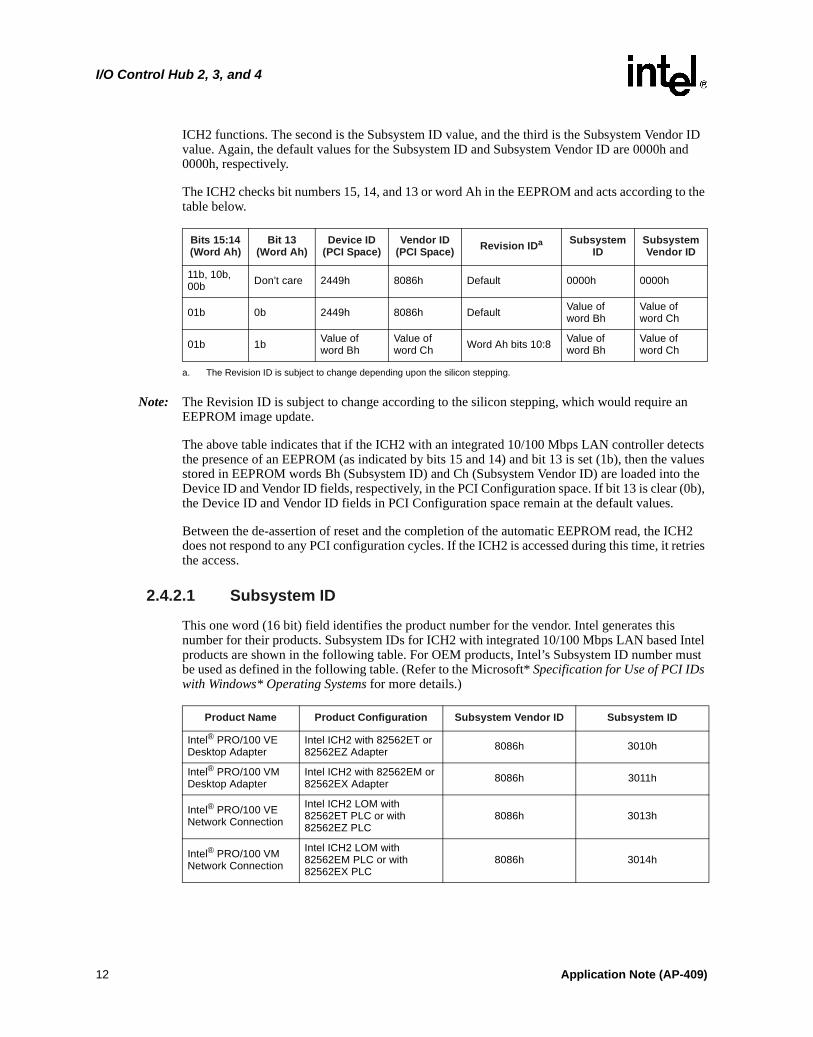
ICH2 functions. The second is the Subsystem ID value, and the third is the Subsystem Vendor ID value. Again, the default values for the Subsystem ID and Subsystem Vendor ID are 0000h and 0000h, respectively.
The ICH2 checks bit numbers 15, 14, and 13 or word Ah in the EEPROM and acts according to the table below.
Note: The Revision ID is subject to change according to the silicon stepping, which would require an EEPROM image update.
The above table indicates that if the ICH2 with an integrated 10/100 Mbps LAN controller detects the presence of an EEPROM (as indicated by bits 15 and 14) and bit 13 is set (1b), then the values stored in EEPROM words Bh (Subsystem ID) and Ch (Subsystem Vendor ID) are loaded into the Device ID and Vendor ID fields, respectively, in the PCI Configuration space. If bit 13 is clear (0b), the Device ID and Vendor ID fields in PCI Configuration space remain at the default values.
Between the de-assertion of reset and the completion of the automatic EEPROM read, the ICH2 does not respond to any PCI configuration cycles. If the ICH2 is accessed during this time, it retries the access.
2.4.2.1 Subsystem ID
This one word (16 bit) field identifies the product number for the vendor. Intel generates this number for their products. Subsystem IDs for ICH2 with integrated 10/100 Mbps LAN based Intel products are shown in the following table. For OEM products, Intel’s Subsystem ID number must be used as defined in the following table. (Refer to the Microsoft* Specification for Use of PCI IDs with Windows* Operating Systems for more details.)
Bits 15:14 (Word Ah)
Bit 13(Word Ah)
Device ID (PCI Space)
Vendor ID (PCI Space) Revision IDa Subsystem
IDSubsystem Vendor ID
11b, 10b, 00b Don’t care 2449h 8086h Default 0000h 0000h
01b 0b 2449h 8086h Default Value of word Bh
Value of word Ch
01b 1b Value of word Bh
Value of word Ch Word Ah bits 10:8 Value of
word BhValue of word Ch
a. The Revision ID is subject to change depending upon the silicon stepping.
Product Name Product Configuration Subsystem Vendor ID Subsystem ID
Intel® PRO/100 VE Desktop Adapter
Intel ICH2 with 82562ET or 82562EZ Adapter 8086h 3010h
Intel® PRO/100 VM Desktop Adapter
Intel ICH2 with 82562EM or 82562EX Adapter 8086h 3011h
Intel® PRO/100 VE Network Connection
Intel ICH2 LOM with 82562ET PLC or with 82562EZ PLC
8086h 3013h
Intel® PRO/100 VM Network Connection
Intel ICH2 LOM with 82562EM PLC or with 82562EX PLC
8086h 3014h
12 Application Note (AP-409)

I/O Control Hub 2, 3, and 4
2.4.2.2 Subsystem Vendor ID
This one word (16 bit) field identifies the OEM vendor. The code used for a particular vendor is the same code assigned as the Vendor ID by the PCI SIG. For OEM products, Intel's Subsystem Vendor ID number must be used as defined in the above table. (Refer to the Microsoft* Specification for Use of PCI IDs with Windows* Operating Systems for more details.)
2.4.2.3 Subsystem ID Settings for 2002 Design1
The ICH2 with integrated LAN provides support for a configurable Subsystem ID. This one word (16 bit) field identifies the product number for the vendor. The Subsystem ID field identifies the ICH2-based specific solution implemented by the vendor. For OEM products, the OEM's Subsystem ID number must be used.
(Refer to the Microsoft* Specification for Use of PCI IDs with Windows* Operating Systems for more details.)
2.4.2.4 Subsystem Vendor ID Settings for 2002 Design
The ICH2 with integrated LAN provides support for configurable Subsystem Vendor ID. This one word (16 bit) field identifies the OEM vendor. The code used for a particular vendor is the same code assigned as the Vendor ID by the PCI SIG. For OEM products, the OEM's Subsystem Vendor ID number must be used.
(Refer to the Microsoft* Specification for Use of PCI IDs with Windows* Operating Systems for more details.)
Intel® PRO/100 P Mobile Combo Adapter
Intel ICH2 with 82562EP Adapter 8086h 3016h
Intel® PRO/100 P Mobile Adapter
Intel ICH2 with 82562EP Adapter 8086h 3017h
Intel® PRO/100 Network Connection
Intel ICH2 LOM with 82562EP PLC 8086h 3018h
Product Name Product Configuration Subsystem Vendor ID Subsystem ID
1. Intel ICH2 (82801BA/BAM chipset) LAN 2002 design. The need for supporting new HPNA devices has been removed from the software release 5.1.3 for the Intel® PRO 100 LAN Adapter. This will allow Intel to have a generic install for ICH2 devices where the PHY is the Intel 82562 Ethernet product. This change will allow customers to comply with Microsoft’s guidelines for using the Subsystem ID information to identify the manufacturer of the motherboard. Intel will no longer require customers to use ICH2 subsystem device ID’s (3010h-3018h). To meet Microsoft requirements customers are required to use their own Subsystem Vendor ID and Subsystem ID (SVID/SID) in Word 0Bh, and Word 0Ch of the EEPROM. See more detain in TA-136.
Application Note (AP-409) 13
I/O Control Hub 2, 3, and 4
2.4.3 ICH3 Integrated 10/100 Mbps LAN Controller Product Identification
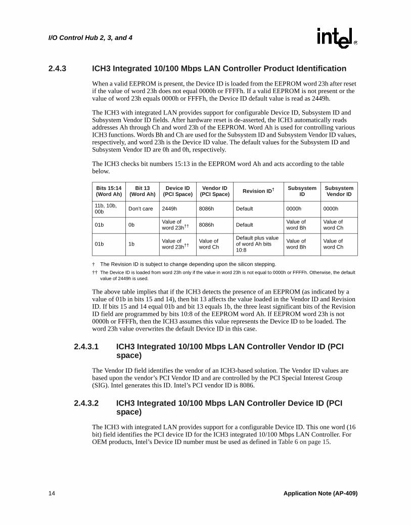
When a valid EEPROM is present, the Device ID is loaded from the EEPROM word 23h after reset if the value of word 23h does not equal 0000h or FFFFh. If a valid EEPROM is not present or the value of word 23h equals 0000h or FFFFh, the Device ID default value is read as 2449h.
The ICH3 with integrated LAN provides support for configurable Device ID, Subsystem ID and Subsystem Vendor ID fields. After hardware reset is de-asserted, the ICH3 automatically reads addresses Ah through Ch and word 23h of the EEPROM. Word Ah is used for controlling various ICH3 functions. Words Bh and Ch are used for the Subsystem ID and Subsystem Vendor ID values, respectively, and word 23h is the Device ID value. The default values for the Subsystem ID and Subsystem Vendor ID are 0h and 0h, respectively.
The ICH3 checks bit numbers 15:13 in the EEPROM word Ah and acts according to the table below.
† The Revision ID is subject to change depending upon the silicon stepping.†† The Device ID is loaded from word 23h only if the value in word 23h is not equal to 0000h or FFFFh. Otherwise, the default
value of 2449h is used.
The above table implies that if the ICH3 detects the presence of an EEPROM (as indicated by a value of 01b in bits 15 and 14), then bit 13 affects the value loaded in the Vendor ID and Revision ID. If bits 15 and 14 equal 01b and bit 13 equals 1b, the three least significant bits of the Revision ID field are programmed by bits 10:8 of the EEPROM word Ah. If EEPROM word 23h is not 0000h or FFFFh, then the ICH3 assumes this value represents the Device ID to be loaded. The word 23h value overwrites the default Device ID in this case.
2.4.3.1 ICH3 Integrated 10/100 Mbps LAN Controller Vendor ID (PCI space)
The Vendor ID field identifies the vendor of an ICH3-based solution. The Vendor ID values are based upon the vendor’s PCI Vendor ID and are controlled by the PCI Special Interest Group (SIG). Intel generates this ID. Intel’s PCI vendor ID is 8086.
2.4.3.2 ICH3 Integrated 10/100 Mbps LAN Controller Device ID (PCI space)
The ICH3 with integrated LAN provides support for a configurable Device ID. This one word (16 bit) field identifies the PCI device ID for the ICH3 integrated 10/100 Mbps LAN Controller. For OEM products, Intel’s Device ID number must be used as defined in Table 6 on page 15.
Bits 15:14 (Word Ah)
Bit 13(Word Ah)
Device ID (PCI Space)
Vendor ID (PCI Space) Revision ID† Subsystem
IDSubsystem Vendor ID
11b, 10b, 00b Don’t care 2449h 8086h Default 0000h 0000h
01b 0b Value of word 23h†† 8086h Default Value of
word BhValue of word Ch
01b 1b Value of word 23h††
Value of word Ch
Default plus value of word Ah bits 10:8
Value of word Bh
Value of word Ch
14 Application Note (AP-409)
I/O Control Hub 2, 3, and 4
2.4.3.3 ICH3 Integrated 10/100 Mbps LAN Controller Subsystem ID (word Bh)
The ICH3 with integrated LAN provides support for a configurable Subsystem ID. This one word (16 bit) field identifies the product number for the vendor. The Subsystem ID field identifies the ICH3-based specific solution implemented by the vendor. For OEM products, the OEM’s Subsystem ID number must be used.
2.4.3.4 ICH3 Integrated 10/100 Mbps LAN Controller Subsystem Vendor ID (word Ch)
The ICH3 with integrated LAN provides support for configurable Subsystem Vendor ID. This one word (16 bit) field identifies the OEM vendor. The code used for a particular vendor is the same code assigned as the Vendor ID by the PCI SIG. For OEM products, the OEM's Subsystem Vendor ID number must be used.
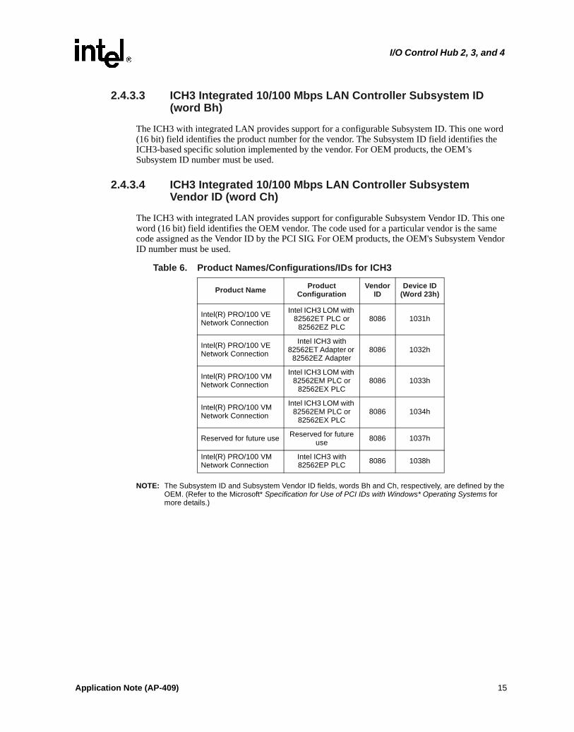
NOTE: The Subsystem ID and Subsystem Vendor ID fields, words Bh and Ch, respectively, are defined by the OEM. (Refer to the Microsoft* Specification for Use of PCI IDs with Windows* Operating Systems for more details.)
Table 6. Product Names/Configurations/IDs for ICH3
Product Name ProductConfiguration
Vendor ID
Device ID(Word 23h)
Intel(R) PRO/100 VE Network Connection
Intel ICH3 LOM with 82562ET PLC or
82562EZ PLC8086 1031h
Intel(R) PRO/100 VE Network Connection
Intel ICH3 with 82562ET Adapter or
82562EZ Adapter8086 1032h
Intel(R) PRO/100 VM Network Connection
Intel ICH3 LOM with 82562EM PLC or
82562EX PLC8086 1033h
Intel(R) PRO/100 VM Network Connection
Intel ICH3 LOM with 82562EM PLC or
82562EX PLC8086 1034h
Reserved for future use Reserved for future use 8086 1037h
Intel(R) PRO/100 VM Network Connection
Intel ICH3 with 82562EP PLC 8086 1038h
Application Note (AP-409) 15

I/O Control Hub 2, 3, and 4
2.4.4 ICH4 Integrated 10/100 Mbps LAN Controller Product Identification
When a valid EEPROM is present, the Device ID is loaded from the EEPROM word 23h after reset
if the value of word 23h does not equal 0000h or FFFFh. If a valid EEPROM is not present or the value of word 23h equals 0000h or FFFFh, the Device ID default value is read as 103Ah. The ICH4 with integrated LAN provides support for configurable Device ID, Subsystem ID and Subsystem Vendor ID fields. After hardware reset is de-asserted, the ICH4 automatically reads addresses Ah through Ch and word 23h of the EEPROM. Word Ah is used for controlling various ICH4 functions. Words Bh and Ch are used for the Subsystem ID and Subsystem Vendor ID values, respectively, and word 23h is the Device ID value. The default values for the Subsystem ID and Subsystem Vendor ID are 0h and 0h, respectively. The ICH4 checks bit numbers 15:13 in the EEPROM word Ah and acts according to the table below:
The above table implies that if the ICH4 detects the presence of an EEPROM (as indicated by a value of 01b in bits 15 and 14), then bit 13 affects the value loaded in the Vendor ID and Revision ID. If bits 15 and 14 equal 01b and bit 13 equals 1b, the three least significant bits of the Revision ID field are programmed by bits 10:8 of the EEPROM word Ah. If EEPROM word 23h is not 0000h or FFFFh, then the ICH4 assumes this value represents the Device ID to be loaded. The word 23h value overwrites the default Device ID in this case.
2.4.4.1 ICH4 Integrated 10/100 Mbps LAN Controller Vendor ID (PCI space)
The Vendor ID field identifies the vendor of an ICH4 based solution. The Vendor ID values are based upon the vendor's PCI Vendor ID and are controlled by the PCI Special Interest Group (SIG). Intel generates this ID. Intel's PCI vendor ID is 8086.
2.4.4.2 ICH4 Integrated 10/100 Mbps LAN Controller Device ID (PCI space)
The ICH4 with integrated LAN provides support for a configurable Device ID. This one word (16-bit) field identifies the PCI device ID for the ICH4 integrated 10/100 Mbps LAN Controller. For OEM products, Intel's Device ID number must be used as defined in Table 7.
Bits 15:14 (Word A)
Bit 13(Word A)
Device IDa (PCI Space)
Vendor ID (PCI Space) Revision IDb Subsystem
IDSubsystem Vendor ID
11b, 10b, 00b Don’t care 103Ah 8086h Default 0000h 0000h
01b 0b Value of word 23h 8086h Default Value of
Word BhValue of Word Ch
01b 1b Value of word 23h
Value of word Ch
Default plus value of Word Ah Bits 10:8
Value of Word Bh
Value of Word Ch
a. The Device ID is loaded from word 23h only if the value in word 23h is not equal to 0000h or FFFFh. Otherwise, the defaultvalue of 103Ah is used.
b. The Revision ID is subject to change depending upon the silicon stepping.
16 Application Note (AP-409)

I/O Control Hub 2, 3, and 4
2.4.4.3 ICH4 Integrated 10/100 Mbps LAN Controller Subsystem ID (word Bh)
The ICH4 with integrated LAN provides support for a configurable Subsystem ID. This one word (16 bit) field identifies the product number for the vendor. The Subsystem ID field identifies the ICH4 based specific solution implemented by the vendor. For OEM products, the OEM's Subsystem ID number must be used.
2.4.4.4 ICH4 Integrated 10/100 Mbps LAN Controller Subsystem Vendor ID (word Ch)
The ICH4 with integrated LAN provides support for configurable Subsystem Vendor ID. This one word (16 bit) field identifies the OEM vendor. The code used for a particular vendor is the same code assigned as the Vendor ID by the PCI SIG. For OEM products, the OEM's Subsystem Vendor ID number must be used.
NOTE: The Subsystem ID and Subsystem Vendor ID fields, words Bh and Ch, respectively, are defined by the OEM. (Refer to the Microsoft* Specification for Use of PCI IDs with Windows* Operating Systems for more details.)
Table 7. Product Names/Configurations IDs for ICH4
Product Name Product Configuration Vendor ID Device ID(Word 23h)
Intel® PRO/100 VE Network Connection
Intel ICH4 LOM with 82562ET PLC or 82562EZ PLC
8086h 1039h
Intel® PRO/100 VE Network Connection
Intel ICH4 with 82562ET Adapter or 82562EZ Adapter
8086h 103Ah
Intel® PRO/100 VM Network Connection
Intel ICH4 LOM with 82562EM PLC or 82562EX PLC
8086h 103Bh
Intel® PRO/100 VM Network Connection
Intel ICH4 with 82562EM Adapter or 82562EX Adapter
8086h 103Ch
Intel® PRO/100 VE Network Connection
Intel ICH4 LOM or Mobile LOM with 82562ET PLC or 82562EZ PLC
8086h 103Dh
Intel® PRO/100 VM Network Connection
Intel ICH4 LOM or Mobile LOM with 82562EM, 82562EP or PLC or 82562EX PLC
8086h 103Eh
Application Note (AP-409) 17

I/O Control Hub 2, 3, and 4
2.5 Integrated Alert on LAN Information
The ICH2, ICH3, ICH4 includes integrated Alert on LAN support.
2.5.1 SMB Address and Heartbeat Packet Pointer
In PCI systems word Dh contains the ICH2, ICH3, and ICH4 SMB address.
NOTE: When using Alert on LAN software these fields should be 007Fh at the factory. Both the SMBus Address and the heartbeat pointer in this field will be configured by the Alert on LAN software when it initializes.
2.5.1.1 Word 40h
This field must be configured to 0044h for proper operation. OEMs must ensure that word 40h in the EEPROM image is set to 0044h (not FFFFh). Word 40h contains pointers for the internal micro-machine, and an incorrect setting lockups the controller. This condition applies to the 82562EP/EM and 82562EX devices (Basic Alerting).
2.5.2 Heartbeat Packet Structure within the EEPROM
The EEPROM may contain a heartbeat packet. The Alert on LAN driver loads the heartbeat packet during configuration. The packet format in the EEPROM is matched but not limited to a UDP packet type. The offset of the system health indication and the offset of the UDP checksum are both even byte. If a value of FFh is used in the checksum word, a checksum calculation is not performed by the ICH2, ICH3, and ICH4. An FFh value can be used for packet formats other than the UDP packet.
Bits Field Description
15 ReservedReserved. For the ICH2, ICH3 and ICH4 this bit is set to 0b.
14 Alert on LAN Enabled
Alert on LAN Enabled. This bit specifies whether Alert on LAN is enabled:0b specifies that Alert on LAN is NOT enabled1b specifies that Alert on LAN is enabled
11:8 Heartbeat Pointer
Alert on LAN Heartbeat Pointer/Reserved. This field points to the location of the heartbeat packet within the EEPROM. The pointers are expressed in a granularity of 16 words. A zero value is not permitted as a valid pointer.For the ICH2, ICH3 and ICH4, a value of 44h is used.
7:0 SMB Address
SMB Address. In a PCI system, this eight bit field holds the ICH2, ICH3, and ICH4 address on the SMB address bus. However, bit seven is ignored. As a result, the address programmed into the EEPROM must be shifted right one bit. For example, address C8h is programmed as address 64h in bits 7:0.
18 Application Note (AP-409)

I/O Control Hub 2, 3, and 4
Figure 1. Heartbeat Packet Example
TCO Packet Pointer(Word D)
EEPROM Packet Length(byte count)
System HealthOffset
(even byte)
ChecksumOffset
(even byte)
Packet Checksum
Heartbeat Packet
Application Note (AP-409) 19
I/O Control Hub 2, 3, and 4
Assume the following example:
• EEPROM packet length N
• Checksum offset 40h
• System health offset N
Thus, the transmitted bytes on the wire would be:
1. Bytes: 0, 1, 2, …, 3F from the EEPROM.
2. Checksum bytes (read bytes 40 and 41, recalculate the checksum, and transmit).
3. Bytes: 42, 43, …, N-1.
4. System health bytes from the I/O Control Hub.
5. Padding bytes (if the packet length is smaller than 64 bytes).
6. Add four bytes of CRC.
Note: The length of the data bytes (not including padding and CRC) is: N + 4.
2.6 Boot Agent Configuration Information
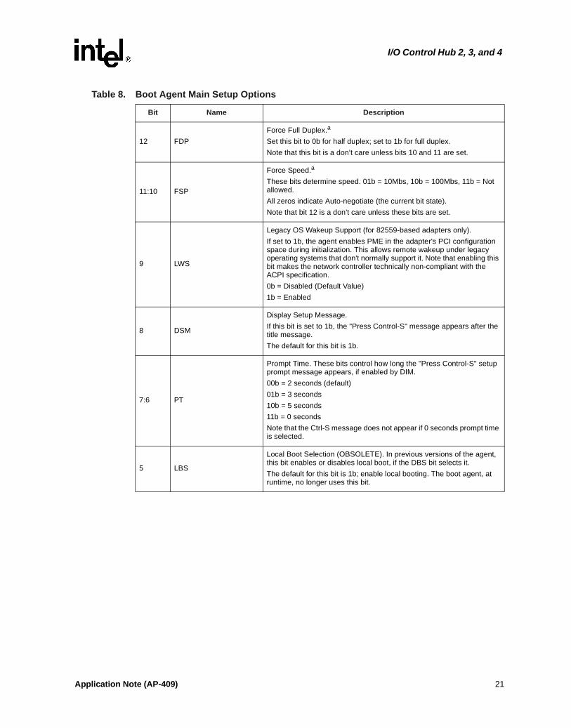
2.6.1 Boot Agent Main Setup Options (Word 30h)
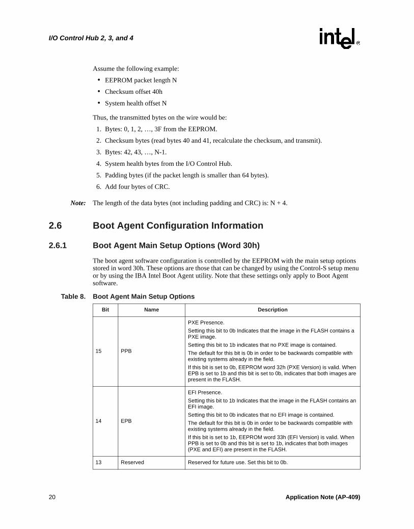
The boot agent software configuration is controlled by the EEPROM with the main setup options stored in word 30h. These options are those that can be changed by using the Control-S setup menu or by using the IBA Intel Boot Agent utility. Note that these settings only apply to Boot Agent software.
Table 8. Boot Agent Main Setup Options
Bit Name Description
15 PPB
PXE Presence.Setting this bit to 0b Indicates that the image in the FLASH contains a PXE image.Setting this bit to 1b indicates that no PXE image is contained. The default for this bit is 0b in order to be backwards compatible with existing systems already in the field.If this bit is set to 0b, EEPROM word 32h (PXE Version) is valid. When EPB is set to 1b and this bit is set to 0b, indicates that both images are present in the FLASH.
14 EPB
EFI Presence.Setting this bit to 1b Indicates that the image in the FLASH contains an EFI image.Setting this bit to 0b indicates that no EFI image is contained. The default for this bit is 0b in order to be backwards compatible with existing systems already in the field.If this bit is set to 1b, EEPROM word 33h (EFI Version) is valid. When PPB is set to 0b and this bit is set to 1b, indicates that both images (PXE and EFI) are present in the FLASH.
13 Reserved Reserved for future use. Set this bit to 0b.
20 Application Note (AP-409)
I/O Control Hub 2, 3, and 4
12 FDPForce Full Duplex.a
Set this bit to 0b for half duplex; set to 1b for full duplex.Note that this bit is a don’t care unless bits 10 and 11 are set.
11:10 FSP
Force Speed.a
These bits determine speed. 01b = 10Mbs, 10b = 100Mbs, 11b = Not allowed.All zeros indicate Auto-negotiate (the current bit state). Note that bit 12 is a don’t care unless these bits are set.
9 LWS
Legacy OS Wakeup Support (for 82559-based adapters only).If set to 1b, the agent enables PME in the adapter's PCI configuration space during initialization. This allows remote wakeup under legacy operating systems that don't normally support it. Note that enabling this bit makes the network controller technically non-compliant with the ACPI specification.0b = Disabled (Default Value)1b = Enabled
8 DSM
Display Setup Message. If this bit is set to 1b, the "Press Control-S" message appears after the title message. The default for this bit is 1b.
7:6 PT
Prompt Time. These bits control how long the "Press Control-S" setup prompt message appears, if enabled by DIM.00b = 2 seconds (default)01b = 3 seconds10b = 5 seconds11b = 0 secondsNote that the Ctrl-S message does not appear if 0 seconds prompt time is selected.
5 LBS
Local Boot Selection (OBSOLETE). In previous versions of the agent, this bit enables or disables local boot, if the DBS bit selects it. The default for this bit is 1b; enable local booting. The boot agent, at runtime, no longer uses this bit.
Table 8. Boot Agent Main Setup Options
Bit Name Description
Application Note (AP-409) 21

I/O Control Hub 2, 3, and 4
4:3 DBS
Default Boot Selection. These bits select which device is the default boot device. These bits are only used if the agent detects that the BIOS does not support boot order selection or if the MODE field of word 31h is set to MODE_LEGACY.00b = Network boot, then local boot01b = Local boot, then network boot10b = Network boot only11b = Local boot only
2 BBS
BIOS Boot Specification (OBSOLETE). In previous versions of the agent, this bit enables or disables use of the BBS to determine boot order. If set to 1b, the BIOS boot order is used, and the DBS bits are ignored. The boot agent at runtime no longer uses this bit. The runtime checks for BBS/PnP and the setting in the MODE field of word 31h are used instead.
1:0 PS
Protocol Select. These bits select the boot protocol.00b = PXE (default value) 01b = RPL protocol Other values are undefined.
a. This setting only applies to the Boot Agent software.
Table 8. Boot Agent Main Setup Options
Bit Name Description
22 Application Note (AP-409)

I/O Control Hub 2, 3, and 4
2.6.2 Boot Agent Configuration Customization Options (Word 31h)
Word 31h contains settings that can be programmed by an OEM or network administrator to customize the operation of the software. These settings cannot be changed from within the Control-S setup menu or the IBA Intel Boot Agent utility. The lower byte contains settings that would typically be configured by a network administrator using the Intel Boot Agent utility; these settings generally control which setup menu options are changeable. The upper byte are generally settings that would be used by an OEM to control the operation of the agent in a LOM environment, although there is nothing in the agent to prevent their use on a NIC implementation.
Table 9. Boot Agent Configuration Customization Options (Word 31h)
Bit Name Description
15:14 SIG Signature. These bits must be set to 1b to indicate that this word has been programmed by the agent or other configuration software.
13:11 Reserved Reserved for future use. Set these bits to 0b.
10:8 MODE
Selects the agent's boot order setup mode. This field changes the agent's default behavior in order to make it compatible with systems that do not completely support the BBS and PnP Expansion ROM standards. Valid values and their meanings are:000b - Normal behavior. The agent attempts to detect BBS and PnP Expansion ROM support as it normally does.001b - Force Legacy mode. The agent does not attempt to detect BBS or PnP Expansion ROM supports in the BIOS and assumes the BIOS is not compliant. The BIOS boot order can be changed in the Setup Menu.010b - Force BBS mode. The agent assumes the BIOS is BBS-compliant, even though it may not be detected as such by the agent's detection code. The BIOS boot order CANNOT be changed in the Setup Menu.011b - Force PnP Int18 mode. The agent assumes the BIOS allows boot order setup for PnP Expansion ROMs and hooks interrupt 18h (to inform the BIOS that the agent is a bootable device) in addition to registering as a BBS IPL device. The BIOS boot order CANNOT be changed in the Setup Menu.100b - Force PnP Int19 mode. The agent assumes the BIOS allows boot order setup for PnP Expansion ROMs and hooks interrupt 19h (to inform the BIOS that the agent is a bootable device) in addition to registering as a BBS IPL device. The BIOS boot order CANNOT be changed in the Setup Menu.101b - Reserved for future use. If specified, treated as value 000b.110b - Reserved for future use. If specified, treated as value 000b.111b - Reserved for future use. If specified, treated as value 000b.
7:6 Reserved Reserved for future use. Set these bits to 0b.
5 DFU
Disable FLASH Update. If set to 1b, no updates to the FLASH image using PROSet is allowed.The default for this bit is 0b; allow FLASH image updates using PROSet.
4 DLWS
Disable Legacy Wakeup Support. If set to 1b, no changes to the Legacy OS Wakeup Support menu option is allowed.The default for this bit is 0b; allow Legacy OS Wakeup Support menu option changes.
Application Note (AP-409) 23

I/O Control Hub 2, 3, and 4
2.6.3 Boot Agent Configuration Customization Options (Word 32h)
Word 32h is used to store the version of the boot agent that is stored in the FLASH image. When the Boot Agent loads, it can check this value to determine if any first-time configuration needs to be performed. The agent then updates this word with its version. Some diagnostic tools to report the version of the Boot Agent in the FLASH also read this word. This word is only valid if the PPB is set to 0b. Otherwise the contents may be undefined.
3 DBSDisable Boot Selection. If set to 1b, no changes to the boot order menu option is allowed.The default for this bit 0b; allow boot order menu option changes.
2 DPSDisable Protocol Select. If set to 1b, no changes to the boot protocol is allowed.The default for this bit is 0b; allow changes to the boot protocol.
1 DTM
Disable Title Message. If set to 1b, the title message displaying the version of the boot agent is suppressed; the Control-S message is also suppressed. This is for OEMs who do not wish the boot agent to display any messages at system boot. The default for this bit is 0b; allow the title message that displays the version of the boot agent and the Control-S message.
0 DSM
Disable Setup Menu. If set to 1b, no invoking the setup menu by pressing Control-S is allowed. In this case, the EEPROM can only be changed via an external program. The default for this bit is 0b; allow invoking the setup menu by pressing Control-S.
Table 9. Boot Agent Configuration Customization Options (Word 31h)
Bit Name Description
Table 10. Boot Agent Configuration Customization Options (Word 32h)
Bit Name Description
15:12 MAJOR PXE boot agent major version. The default for these bits is 0b.
11:8 MINOR PXE boot agent minor version. The default for these bits is 0b.
7:0 BUILD PXE boot agent build number. The default for these bits is 0b.
24 Application Note (AP-409)

I/O Control Hub 2, 3, and 4
2.6.4 IBA Capabilities (Word 33h)
Word 33h is used to enumerate the boot technologies that have been programmed into the FLASH. It is updated by IBA configuration tools and is not updated or read by IBA.
2.7 Checksum
The Checksum word is calculated by adding all of the EEPROM words (00h through FFh, based on a 256-register EEPROM), including the Checksum word itself. The sum should equal BABAh. The initial value before the values are added together should be 0000h, and the carry bit should be ignored after each addition. This checksum can be located at 3Fh or FFh depending on the size of the EEPROM.
Table 11. IBA Capabilities
Bit Name Description
15:14 SIG Signature. These bits must be set to 1b to indicate that this word has been programmed by the agent or other configuration software.
13:5 Reserved Reserved for future use. Set these bits to 0b.
4 SANSAN capability is present in FLASH.0b = The SAN capability is not present (default).1b = The SAN capability is present.
3 EFIEFI UNDI capability is present in FLASH.0b = The RPL code is not present (default).1b = The RPL code is present.
2 RPLRPL capability is present in FLASH.1b = The RPL code is present (default).0b = The RPL code is not present.
1 UNDIPXE/UNDI capability is present in FLASH.1b = The PXE base code is present (default).0b = The PXE base code is not present.
0 BCPXE base code is present in FLASH.0b = The PXE base code is present (default).1b = The PXE base code is not present.
Application Note (AP-409) 25

I/O Control Hub 2, 3, and 4
Note: This page intentionally left blank.
26 Application Note (AP-409)

I/O Control Hub 2, 3, and 4
Appendix A: ICH2 EEPROM Contents
This appendix contains a sample of raw EEPROM contents for the ICH2. All values for these images are hexadecimal.
A.1 82562ET EEPROM Image with ICH2
Note: "XXXX" denotes the Individual Address, "YYYY" denotes the checksum, and "ZZZZ" is the Subsystem ID field and "WWWW" is the Subvendor ID field.
XXXX XXXX XXXX 1A03 0000 0201 4701 0000
0000 0000 49A2 ZZZZ WWWW 007F 0000 0000
0000 0000 0000 0000 0000 0000 0000 0000
0000 0000 0000 0000 0000 0000 0000 0000
0000 0000 0000 0000 0000 0000 0000 0000
0000 0000 0000 0000 0000 0000 0000 0000
002C 0000 0000 0000 0000 0000 0000 0000
0000 0000 0000 4030 0000 0000 0000 YYYY
A.2 82562EM EEPROM Image with ICH2
Note: "XXXX" denotes the Individual Address, "YYYY" denotes the checksum, and "ZZZZ" is the Subsystem ID field and "WWWW" is the Subvendor ID field.
XXXX XXXX XXXX 1A13 0000 0201 4701 0000
0000 0000 49A2 ZZZZ WWWW 007F 0000 0000
0000 0000 0000 0000 0000 0000 0000 0000
Table 12. ICH2 EEPROM Contents
Word Description
0:2h Ethernet Individual Address
3h Compatibility Bytes
5h Controller and Connector Type
6h PHY Device Record
8:9h PWA Bytes
Ah EEPROM ID
Bh Subsystem ID
Ch Subsystem Vendor ID
Dh Heartbeat Packet Pointer and SMB Address Field
3Fh Checksum for 64-word EEPROM
FFh Checksum for 256-word EEPROM
Application Note (AP-409) 27

I/O Control Hub 2, 3, and 4
0000 0000 0000 0000 0000 0000 0000 0000
0000 0000 0000 0000 0000 0000 0000 0000
0000 0000 0000 0000 0000 0000 0000 0000
002C 0000 0000 0000 0000 0000 0000 0000
0000 0000 0000 4030 0000 0000 0000 0000
0044 0000 0000 0000 0000 0000 0000 0000
0000 0000 0000 0000 0000 0000 0000 0000
0000 0000 0000 0000 0000 0000 0000 0000
0000 0000 0000 0000 0000 0000 0000 0000
0000 0000 0000 0000 0000 0000 0000 0000
0000 0000 0000 0000 0000 0000 0000 0000
0000 0000 0000 0000 0000 0000 0000 0000
0000 0000 0000 0000 0000 0000 0000 0000
0000 0000 0000 0000 0000 0000 0000 0000
0000 0000 0000 0000 0000 0000 0000 0000
0000 0000 0000 0000 0000 0000 0000 0000
0000 0000 0000 0000 0000 0000 0000 0000
0000 0000 0000 0000 0000 0000 0000 0000
0000 0000 0000 0000 0000 0000 0000 0000
0000 0000 0000 0000 0000 0000 0000 0000
0000 0000 0000 0000 0000 0000 0000 0000
0000 0000 0000 0000 0000 0000 0000 0000
0000 0000 0000 0000 0000 0000 0000 0000
0000 0000 0000 0000 0000 0000 0000 0000
0000 0000 0000 0000 0000 0000 0000 0000
0000 0000 0000 0000 0000 0000 0000 0000
0000 0000 0000 0000 0000 0000 0000 0000
0000 0000 0000 0000 0000 0000 0000 0000
0000 0000 0000 0000 0000 0000 0000 YYYY
28 Application Note (AP-409)

I/O Control Hub 2, 3, and 4
A.3 82562EP EEPROM Image with ICH2
Note: "XXXX" denotes the Individual Address, "YYYY" denotes the checksum, and "ZZZZ" is the Subsystem ID field and "WWWW" is the Subvendor ID field.
XXXX XXXX XXXX 1A03 0000 0210 4C01 0000
0000 0000 49A2 ZZZZ WWWW 007F 0000 0000
0000 0000 0000 0000 0000 0000 0000 0000
0000 0000 0000 0000 0000 0000 0000 0000
0000 0000 0000 0000 0000 0000 0000 0000
0000 0000 0000 0000 0000 0000 0000 0000
002C 0000 0000 0000 0000 0000 0000 0000
0000 0000 0000 4030 0000 0000 0000 0000
0044 0000 0000 0000 0000 0000 0000 0000
0000 0000 0000 0000 0000 0000 0000 0000
0000 0000 0000 0000 0000 0000 0000 0000
0000 0000 0000 0000 0000 0000 0000 0000
0000 0000 0000 0000 0000 0000 0000 0000
0000 0000 0000 0000 0000 0000 0000 0000
0000 0000 0000 0000 0000 0000 0000 0000
0000 0000 0000 0000 0000 0000 0000 0000
0000 0000 0000 0000 0000 0000 0000 0000
0000 0000 0000 0000 0000 0000 0000 0000
0000 0000 0000 0000 0000 0000 0000 0000
0000 0000 0000 0000 0000 0000 0000 0000
0000 0000 0000 0000 0000 0000 0000 0000
0000 0000 0000 0000 0000 0000 0000 0000
0000 0000 0000 0000 0000 0000 0000 0000
0000 0000 0000 0000 0000 0000 0000 0000
0000 0000 0000 0000 0000 0000 0000 0000
0000 0000 0000 0000 0000 0000 0000 0000
Application Note (AP-409) 29
I/O Control Hub 2, 3, and 4
0000 0000 0000 0000 0000 0000 0000 0000
0000 0000 0000 0000 0000 0000 0000 0000
0000 0000 0000 0000 0000 0000 0000 0000
0000 0000 0000 0000 0000 0000 0000 0000
0000 0000 0000 0000 0000 0000 0000 0000
0000 0000 0000 0000 0000 0000 0000 YYYY
30 Application Note (AP-409)

I/O Control Hub 2, 3, and 4
Appendix B: ICH3 EEPROM Contents
This appendix contains a sample of raw EEPROM contents for the ICH3. All values for these images are hexadecimal.
B.1 82562ET EEPROM Image with ICH3
Note: "XXXX" denotes the Individual Address, "YYYY" denotes the checksum, and "ZZZZ" is the Subsystem ID field and "WWWW" is the Subvendor ID field.
XXXX XXXX XXXX 1A03 0000 0201 4701 0000
0000 0000 49A2 ZZZZ WWWW 007F 0000 0000
0000 0000 0000 0000 0000 0000 0000 0000
0000 0000 0000 0000 0000 0000 0000 0000
0000 0000 0000 1031 0000 0000 0000 0000
0000 0000 0000 0000 0000 0000 0000 0000
002C 0000 0000 0000 0000 0000 0000 0000
0000 0000 0000 4030 0000 0000 0000 YYYY
B.2 82562EM EEPROM Image with ICH3
Note: "XXXX" denotes the Individual Address, "YYYY" denotes the checksum, and "ZZZZ" is the Subsystem ID field and "WWWW" is the Subvendor ID field.
XXXX XXXX XXXX 1A13 0000 0201 4701 0000
0000 0000 49A2 ZZZZ WWWW 007F 0000 0000
Table 13. ICH3 EEPROM Contents
Word Description
0:2h Ethernet Individual Address
3h Compatibility Bytes
5h Controller and Connector Type
6h PHY Device Record
8:9h PWA Bytes
Ah EEPROM ID
Bh Subsystem ID
Ch Subsystem Vendor ID
Dh Heartbeat Packet Pointer and SMB Address Field
23h ICH3 Device
3Fh Checksum for 64-word EEPROM
FFh Checksum for 256-word EEPROM
Application Note (AP-409) 31

I/O Control Hub 2, 3, and 4
0000 0000 0000 0000 0000 0000 0000 0000
0000 0000 0000 0000 0000 0000 0000 0000
0000 0000 0000 1033 0000 0000 0000 0000
0000 0000 0000 0000 0000 0000 0000 0000
002C 0000 0000 0000 0000 0000 0000 0000
0000 0000 0000 4030 0000 0000 0000 0000
0044 0000 0000 0000 0000 0000 0000 0000
0000 0000 0000 0000 0000 0000 0000 0000
0000 0000 0000 0000 0000 0000 0000 0000
0000 0000 0000 0000 0000 0000 0000 0000
0000 0000 0000 0000 0000 0000 0000 0000
0000 0000 0000 0000 0000 0000 0000 0000
0000 0000 0000 0000 0000 0000 0000 0000
0000 0000 0000 0000 0000 0000 0000 0000
0000 0000 0000 0000 0000 0000 0000 0000
0000 0000 0000 0000 0000 0000 0000 0000
0000 0000 0000 0000 0000 0000 0000 0000
0000 0000 0000 0000 0000 0000 0000 0000
0000 0000 0000 0000 0000 0000 0000 0000
0000 0000 0000 0000 0000 0000 0000 0000
0000 0000 0000 0000 0000 0000 0000 0000
0000 0000 0000 0000 0000 0000 0000 0000
0000 0000 0000 0000 0000 0000 0000 0000
0000 0000 0000 0000 0000 0000 0000 0000
0000 0000 0000 0000 0000 0000 0000 0000
0000 0000 0000 0000 0000 0000 0000 0000
0000 0000 0000 0000 0000 0000 0000 0000
0000 0000 0000 0000 0000 0000 0000 0000
0000 0000 0000 0000 0000 0000 0000 0000
0000 0000 0000 0000 0000 0000 0000 YYYY
32 Application Note (AP-409)
I/O Control Hub 2, 3, and 4
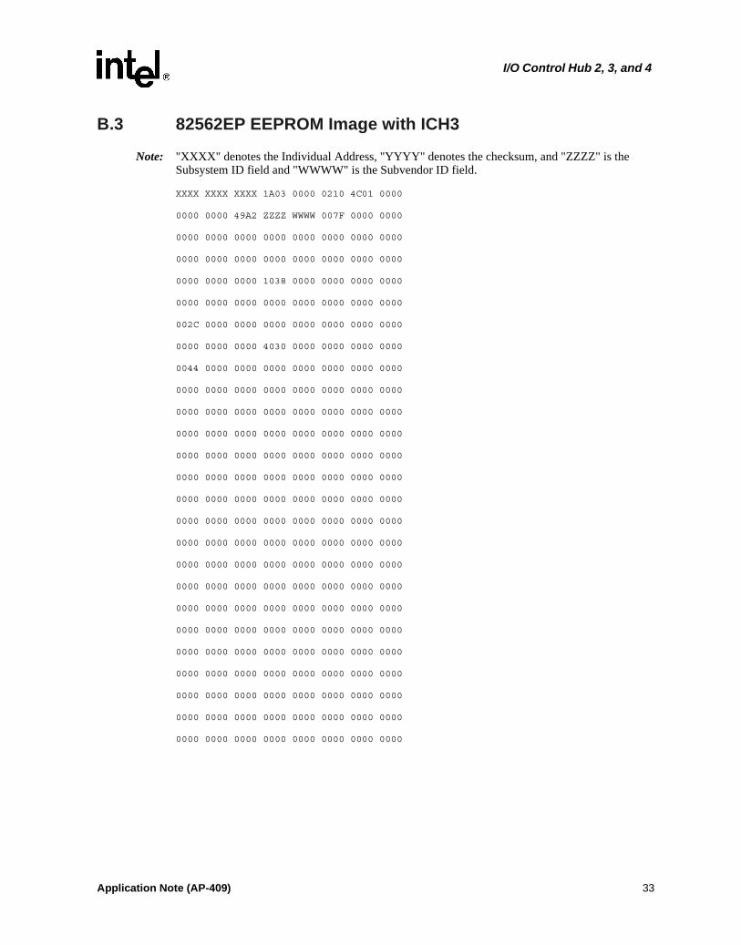
B.3 82562EP EEPROM Image with ICH3
Note: "XXXX" denotes the Individual Address, "YYYY" denotes the checksum, and "ZZZZ" is the Subsystem ID field and "WWWW" is the Subvendor ID field.
XXXX XXXX XXXX 1A03 0000 0210 4C01 0000
0000 0000 49A2 ZZZZ WWWW 007F 0000 0000
0000 0000 0000 0000 0000 0000 0000 0000
0000 0000 0000 0000 0000 0000 0000 0000
0000 0000 0000 1038 0000 0000 0000 0000
0000 0000 0000 0000 0000 0000 0000 0000
002C 0000 0000 0000 0000 0000 0000 0000
0000 0000 0000 4030 0000 0000 0000 0000
0044 0000 0000 0000 0000 0000 0000 0000
0000 0000 0000 0000 0000 0000 0000 0000
0000 0000 0000 0000 0000 0000 0000 0000
0000 0000 0000 0000 0000 0000 0000 0000
0000 0000 0000 0000 0000 0000 0000 0000
0000 0000 0000 0000 0000 0000 0000 0000
0000 0000 0000 0000 0000 0000 0000 0000
0000 0000 0000 0000 0000 0000 0000 0000
0000 0000 0000 0000 0000 0000 0000 0000
0000 0000 0000 0000 0000 0000 0000 0000
0000 0000 0000 0000 0000 0000 0000 0000
0000 0000 0000 0000 0000 0000 0000 0000
0000 0000 0000 0000 0000 0000 0000 0000
0000 0000 0000 0000 0000 0000 0000 0000
0000 0000 0000 0000 0000 0000 0000 0000
0000 0000 0000 0000 0000 0000 0000 0000
0000 0000 0000 0000 0000 0000 0000 0000
0000 0000 0000 0000 0000 0000 0000 0000
Application Note (AP-409) 33
I/O Control Hub 2, 3, and 4
0000 0000 0000 0000 0000 0000 0000 0000
0000 0000 0000 0000 0000 0000 0000 0000
0000 0000 0000 0000 0000 0000 0000 0000
0000 0000 0000 0000 0000 0000 0000 0000
0000 0000 0000 0000 0000 0000 0000 0000
0000 0000 0000 0000 0000 0000 0000 YYYY
B.4 82562EZ EEPROM Image with ICH3
Note: "XXXX" denotes the Individual Address, "YYYY" denotes the checksum, and "ZZZZ" is the Subsystem ID field and "WWWW" is the Subvendor ID field.
XXXX XXXX XXXX 1A03 0000 0201 4701 0000
0000 0000 49A2 ZZZZ WWWW 007F 0000 0000
0000 0000 0000 0000 0000 0000 0000 0000
0000 0000 0000 0000 0000 0000 0000 0000
0000 0000 0000 1031 0000 0000 0000 0000
0000 0000 0000 0000 0000 0000 0000 0000
002C 0000 0000 0000 0000 0000 0000 0000
0000 0000 0000 4030 0000 0000 0000 YYYY
B.5 82562EX EEPROM Image with ICH3
Note: "XXXX" denotes the Individual Address, "YYYY" denotes the checksum, and "ZZZZ" is the Subsystem ID field and "WWWW" is the Subvendor ID field.
XXXX XXXX XXXX 1A13 0000 0201 4701 0000
0000 0000 49A2 ZZZZ WWWW 007F 0000 0000
0000 0000 0000 0000 0000 0000 0000 0000
0000 0000 0000 0000 0000 0000 0000 0000
0000 0000 0000 1033 0000 0000 0000 0000
0000 0000 0000 0000 0000 0000 0000 0000
002C 0000 0000 0000 0000 0000 0000 0000
0000 0000 0000 4030 0000 0000 0000 0000
0044 0000 0000 0000 0000 0000 0000 0000
0000 0000 0000 0000 0000 0000 0000 0000
0000 0000 0000 0000 0000 0000 0000 0000
0000 0000 0000 0000 0000 0000 0000 0000
34 Application Note (AP-409)

I/O Control Hub 2, 3, and 4
0000 0000 0000 0000 0000 0000 0000 0000
0000 0000 0000 0000 0000 0000 0000 0000
0000 0000 0000 0000 0000 0000 0000 0000
0000 0000 0000 0000 0000 0000 0000 0000
0000 0000 0000 0000 0000 0000 0000 0000
0000 0000 0000 0000 0000 0000 0000 0000
0000 0000 0000 0000 0000 0000 0000 0000
0000 0000 0000 0000 0000 0000 0000 0000
0000 0000 0000 0000 0000 0000 0000 0000
0000 0000 0000 0000 0000 0000 0000 0000
0000 0000 0000 0000 0000 0000 0000 0000
0000 0000 0000 0000 0000 0000 0000 0000
0000 0000 0000 0000 0000 0000 0000 0000
0000 0000 0000 0000 0000 0000 0000 0000
0000 0000 0000 0000 0000 0000 0000 0000
0000 0000 0000 0000 0000 0000 0000 0000
0000 0000 0000 0000 0000 0000 0000 0000
0000 0000 0000 0000 0000 0000 0000 0000
0000 0000 0000 0000 0000 0000 0000 0000
0000 0000 0000 0000 0000 0000 0000 YYYY
Application Note (AP-409) 35

I/O Control Hub 2, 3, and 4
Note: This page is intentionally left blank.
36 Application Note (AP-409)
I/O Control Hub 2, 3, and 4
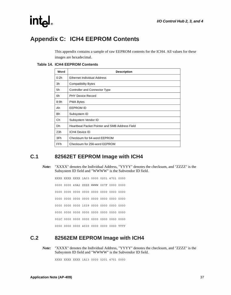
Appendix C: ICH4 EEPROM Contents
This appendix contains a sample of raw EEPROM contents for the ICH4. All values for theseimages are hexadecimal.
C.1 82562ET EEPROM Image with ICH4
Note: "XXXX" denotes the Individual Address, "YYYY" denotes the checksum, and "ZZZZ" is the Subsystem ID field and "WWWW" is the Subvendor ID field.
XXXX XXXX XXXX 1A03 0000 0201 4701 0000
0000 0000 49A2 ZZZZ WWWW 007F 0000 0000
0000 0000 0000 0000 0000 0000 0000 0000
0000 0000 0000 0000 0000 0000 0000 0000
0000 0000 0000 1039 0000 0000 0000 0000
0000 0000 0000 0000 0000 0000 0000 0000
002C 0000 0000 0000 0000 0000 0000 0000
0000 0000 0000 4030 0000 0000 0000 YYYY
C.2 82562EM EEPROM Image with ICH4
Note: "XXXX" denotes the Individual Address, "YYYY" denotes the checksum, and "ZZZZ" is the Subsystem ID field and "WWWW" is the Subvendor ID field.
XXXX XXXX XXXX 1A13 0000 0201 4701 0000
Table 14. ICH4 EEPROM Contents
Word Description
0:2h Ethernet Individual Address
3h Compatibility Bytes
5h Controller and Connector Type
6h PHY Device Record
8:9h PWA Bytes
Ah EEPROM ID
Bh Subsystem ID
Ch Subsystem Vendor ID
Dh Heartbeat Packet Pointer and SMB Address Field
23h ICH4 Device ID
3Fh Checksum for 64-word EEPROM
FFh Checksum for 256-word EEPROM
Application Note (AP-409) 37

I/O Control Hub 2, 3, and 4
0000 0000 49A2 ZZZZ WWWW 007F 0000 0000
0000 0000 0000 0000 0000 0000 0000 0000
0000 0000 0000 0000 0000 0000 0000 0000
0000 0000 0000 103B 0000 0000 0000 0000
0000 0000 0000 0000 0000 0000 0000 0000
002C 0000 0000 0000 0000 0000 0000 0000
0000 0000 0000 4030 0000 0000 0000 0000
0044 0000 0000 0000 0000 0000 0000 0000
0000 0000 0000 0000 0000 0000 0000 0000
0000 0000 0000 0000 0000 0000 0000 0000
0000 0000 0000 0000 0000 0000 0000 0000
0000 0000 0000 0000 0000 0000 0000 0000
0000 0000 0000 0000 0000 0000 0000 0000
0000 0000 0000 0000 0000 0000 0000 0000
0000 0000 0000 0000 0000 0000 0000 0000
0000 0000 0000 0000 0000 0000 0000 0000
0000 0000 0000 0000 0000 0000 0000 0000
0000 0000 0000 0000 0000 0000 0000 0000
0000 0000 0000 0000 0000 0000 0000 0000
0000 0000 0000 0000 0000 0000 0000 0000
0000 0000 0000 0000 0000 0000 0000 0000
0000 0000 0000 0000 0000 0000 0000 0000
0000 0000 0000 0000 0000 0000 0000 0000
0000 0000 0000 0000 0000 0000 0000 0000
0000 0000 0000 0000 0000 0000 0000 0000
0000 0000 0000 0000 0000 0000 0000 0000
0000 0000 0000 0000 0000 0000 0000 0000
0000 0000 0000 0000 0000 0000 0000 0000
0000 0000 0000 0000 0000 0000 0000 0000
0000 0000 0000 0000 0000 0000 0000 0000
0000 0000 0000 0000 0000 0000 0000 YYYY
38 Application Note (AP-409)

I/O Control Hub 2, 3, and 4
C.3 82562EP EEPROM Image with ICH4
Note: "XXXX" denotes the Individual Address, "YYYY" denotes the checksum, and "ZZZZ" is the Subsystem ID field and "WWWW" is the Subvendor ID field.
XXXX XXXX XXXX 1A03 0000 0210 4C01 0000
0000 0000 49A2 ZZZZ WWWW 007F 0000 0000
0000 0000 0000 0000 0000 0000 0000 0000
0000 0000 0000 0000 0000 0000 0000 0000
0000 0000 0000 103E 0000 0000 0000 0000
0000 0000 0000 0000 0000 0000 0000 0000
002C 0000 0000 0000 0000 0000 0000 0000
0000 0000 0000 4030 0000 0000 0000 0000
0044 0000 0000 0000 0000 0000 0000 0000
0000 0000 0000 0000 0000 0000 0000 0000
0000 0000 0000 0000 0000 0000 0000 0000
0000 0000 0000 0000 0000 0000 0000 0000
0000 0000 0000 0000 0000 0000 0000 0000
0000 0000 0000 0000 0000 0000 0000 0000
0000 0000 0000 0000 0000 0000 0000 0000
0000 0000 0000 0000 0000 0000 0000 0000
0000 0000 0000 0000 0000 0000 0000 0000
0000 0000 0000 0000 0000 0000 0000 0000
0000 0000 0000 0000 0000 0000 0000 0000
0000 0000 0000 0000 0000 0000 0000 0000
0000 0000 0000 0000 0000 0000 0000 0000
0000 0000 0000 0000 0000 0000 0000 0000
0000 0000 0000 0000 0000 0000 0000 0000
0000 0000 0000 0000 0000 0000 0000 0000
0000 0000 0000 0000 0000 0000 0000 0000
0000 0000 0000 0000 0000 0000 0000 0000
0000 0000 0000 0000 0000 0000 0000 0000
0000 0000 0000 0000 0000 0000 0000 0000
0000 0000 0000 0000 0000 0000 0000 0000
0000 0000 0000 0000 0000 0000 0000 0000
Application Note (AP-409) 39
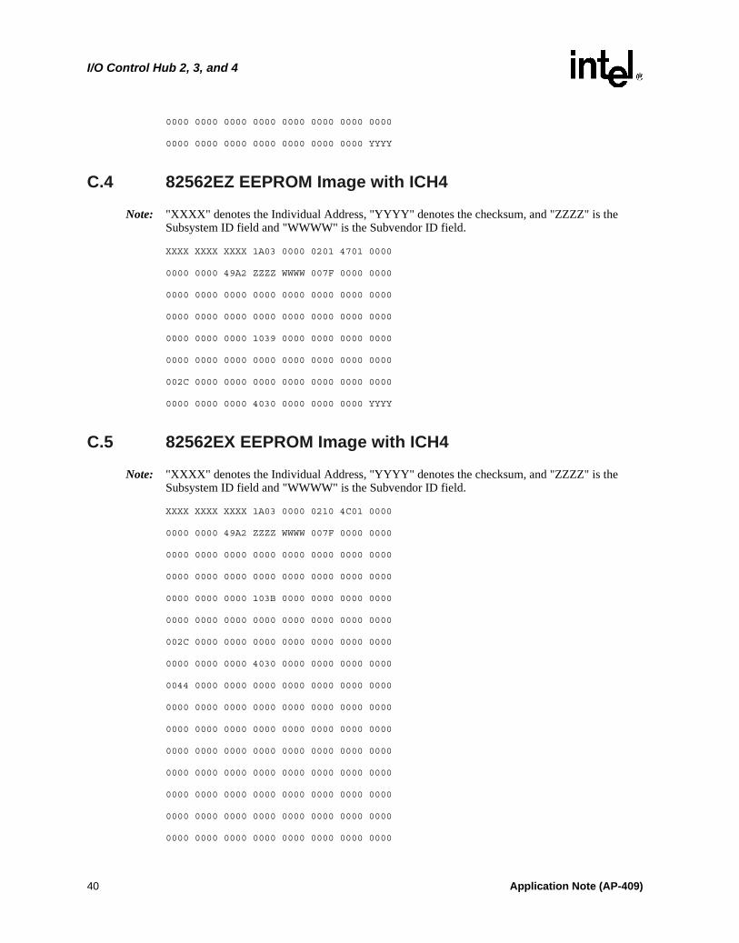
I/O Control Hub 2, 3, and 4
0000 0000 0000 0000 0000 0000 0000 0000
0000 0000 0000 0000 0000 0000 0000 YYYY
C.4 82562EZ EEPROM Image with ICH4
Note: "XXXX" denotes the Individual Address, "YYYY" denotes the checksum, and "ZZZZ" is the Subsystem ID field and "WWWW" is the Subvendor ID field.
XXXX XXXX XXXX 1A03 0000 0201 4701 0000
0000 0000 49A2 ZZZZ WWWW 007F 0000 0000
0000 0000 0000 0000 0000 0000 0000 0000
0000 0000 0000 0000 0000 0000 0000 0000
0000 0000 0000 1039 0000 0000 0000 0000
0000 0000 0000 0000 0000 0000 0000 0000
002C 0000 0000 0000 0000 0000 0000 0000
0000 0000 0000 4030 0000 0000 0000 YYYY
C.5 82562EX EEPROM Image with ICH4
Note: "XXXX" denotes the Individual Address, "YYYY" denotes the checksum, and "ZZZZ" is the Subsystem ID field and "WWWW" is the Subvendor ID field.
XXXX XXXX XXXX 1A03 0000 0210 4C01 0000
0000 0000 49A2 ZZZZ WWWW 007F 0000 0000
0000 0000 0000 0000 0000 0000 0000 0000
0000 0000 0000 0000 0000 0000 0000 0000
0000 0000 0000 103B 0000 0000 0000 0000
0000 0000 0000 0000 0000 0000 0000 0000
002C 0000 0000 0000 0000 0000 0000 0000
0000 0000 0000 4030 0000 0000 0000 0000
0044 0000 0000 0000 0000 0000 0000 0000
0000 0000 0000 0000 0000 0000 0000 0000
0000 0000 0000 0000 0000 0000 0000 0000
0000 0000 0000 0000 0000 0000 0000 0000
0000 0000 0000 0000 0000 0000 0000 0000
0000 0000 0000 0000 0000 0000 0000 0000
0000 0000 0000 0000 0000 0000 0000 0000
0000 0000 0000 0000 0000 0000 0000 0000
40 Application Note (AP-409)

I/O Control Hub 2, 3, and 4
0000 0000 0000 0000 0000 0000 0000 0000
0000 0000 0000 0000 0000 0000 0000 0000
0000 0000 0000 0000 0000 0000 0000 0000
0000 0000 0000 0000 0000 0000 0000 0000
0000 0000 0000 0000 0000 0000 0000 0000
0000 0000 0000 0000 0000 0000 0000 0000
0000 0000 0000 0000 0000 0000 0000 0000
0000 0000 0000 0000 0000 0000 0000 0000
0000 0000 0000 0000 0000 0000 0000 0000
0000 0000 0000 0000 0000 0000 0000 0000
0000 0000 0000 0000 0000 0000 0000 0000
0000 0000 0000 0000 0000 0000 0000 0000
0000 0000 0000 0000 0000 0000 0000 0000
0000 0000 0000 0000 0000 0000 0000 0000
0000 0000 0000 0000 0000 0000 0000 0000
0000 0000 0000 0000 0000 0000 0000 YYYY
Application Note (AP-409) 41

I/O Control Hub 2, 3, and 4
Note: This page is intentionally left blank.
42 Application Note (AP-409)