Embed Size (px)
Citation preview
Electron Diffraction
1 Introduction
It is well established that every “particle” with a rest mass m moving with momentum p can behavelike a “wave” with a wavelength λ given by Louis de Broglie’s relation:
λ =h
p=
h√2mE
. (1)
In this equation, h is Planck’s constant and E = p2/(2m) is the kinetic energy of the particle in thenon-relativistic regime. The wave aspect of particles was demonstrated first by an experiment onelectron diffraction performed by C. H. Davisson and L. H. Germer. For his hypothesis on the wavenature of particles de Broglie was awarded the Nobel Prize in Physics in 1929, and Davisson andGermer received the 1937 Nobel Prize for their experiment. The Davisson and Germer experimenthad a beam of electrons with a well defined wavelength shorter than the spacing between atomsin a target metal crystal reflecting from its surface; at particular angles of reflection they detecteda large increase in the reflected intensity corresponding to diffraction peaks much like one can seenowadays on reflection from a grating using a laser. An elementary description of the de Brogliehypothesis and of the Davisson and Germer experiments can be found in any introductory physicsbook with some modern physics chapters [1, for example]. An excellent description of a moremodern electron source and reflection diffraction from a graphite crystal and the crystal with asingle layer of Krypton atoms on top can be found in the short article by M. D. Chinn and S. C.Fain, Jr. [2].
Our setup is a transmission electron diffraction apparatus, but the physics is similar to the one ofDavisson and Germer. Our apparatus consists of a sealed unit, thus it is not possible to changethe target samples or do adjustments other than the ones on the control panel of the instrument.In these notes we briefly describe the apparatus, provide notes on crystallography which will helpunderstand what is called a “spot” pattern and a “ring” pattern. The same methods and basicdiffraction physics in this experiment are used in more sophisticated diffraction experiments withprotons, positrons, x-rays, light, microwaves, neutrons and atoms (everything with a wavelengthshorter than the distance between the “slits” of the diffraction grating), so this relatively simpleexperiment is a good introduction to a wide range of experimental techniques used in currentresearch.
2 Electron diffraction apparatus
Typical electron diffraction apparatus consists of an electron gun, similar to the ones used in oldoscilloscopes except that the voltage (V ) accelerating the electrons (charge e) can be varied betweenzero and about 10 kilovolts. The accelerating voltage controls the kinetic energy of the electronsemitted from a heated filament (essentially at rest compared to their final velocity). The finalenergy of the electrons (or their momentum) can be found from
eV =p2
2m= E . (2)
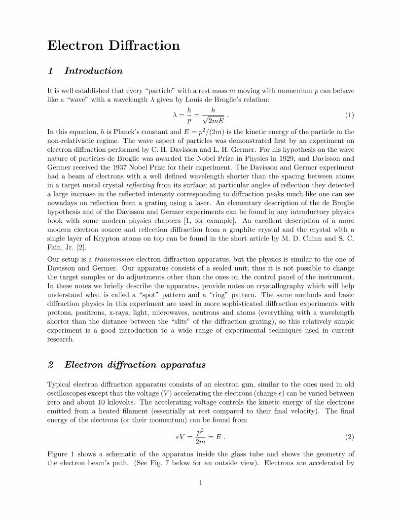
Figure 1 shows a schematic of the apparatus inside the glass tube and shows the geometry ofthe electron beam’s path. (See Fig. 7 below for an outside view). Electrons are accelerated by
1
the potential difference V between the cathode and an anode that they pass through. There arealso additional electrodes (not shown) used to focus the beam. The electrons then drift betweenthe horizontal and vertical deflection plates so that they pass through metal or graphite samplesmounted on a grid. The electrons eventually strike the fluorescent screen. If the sample has analigned single crystal usually one can obtain diffraction “spots” on the screen, while if the sampleis polycrystalline one sees “rings” on the screen.
Figure 1: Schematic of electron tube. The horizontal and vertical deflection plates allow the beamto be steered so that it strikes different sample areas on the sample grid. Notice that the scatteringangle is 2θ, not θ as is used in linear diffraction gratings in optics. The sample grid is much smallerin dimension than what it appears here. See the text for explanation of Bragg diffraction.
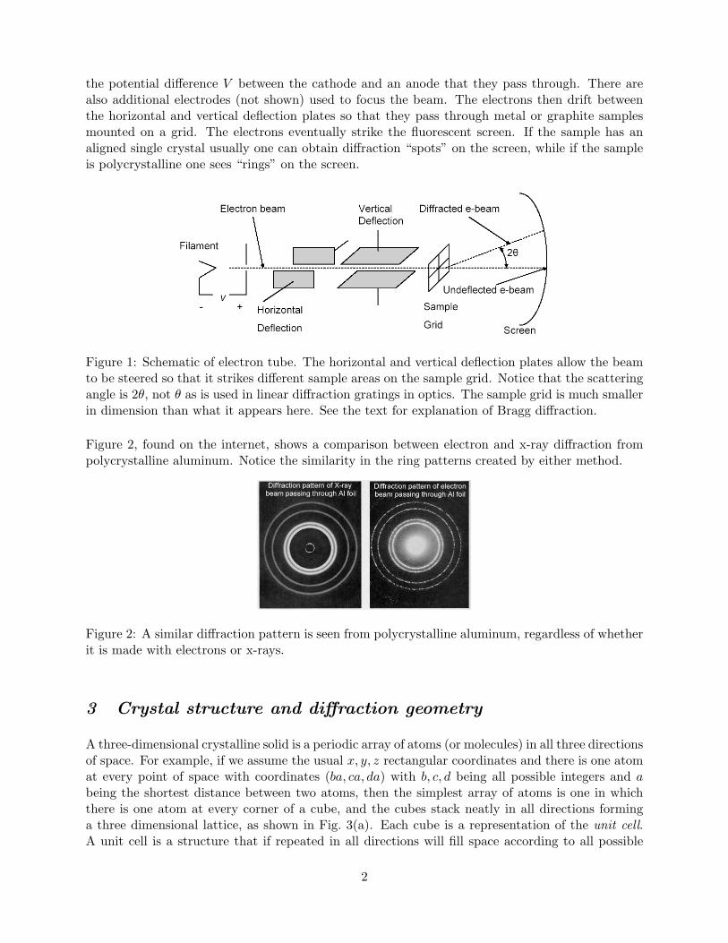
Figure 2, found on the internet, shows a comparison between electron and x-ray diffraction frompolycrystalline aluminum. Notice the similarity in the ring patterns created by either method.
Figure 2: A similar diffraction pattern is seen from polycrystalline aluminum, regardless of whetherit is made with electrons or x-rays.
3 Crystal structure and diffraction geometry
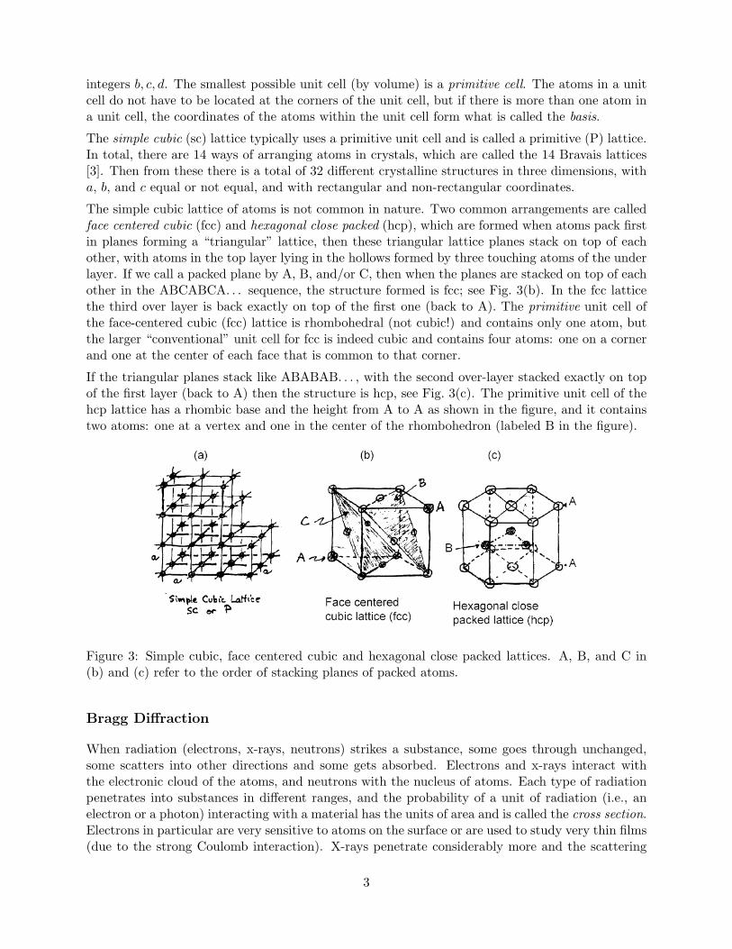
A three-dimensional crystalline solid is a periodic array of atoms (or molecules) in all three directionsof space. For example, if we assume the usual x, y, z rectangular coordinates and there is one atomat every point of space with coordinates (ba, ca, da) with b, c, d being all possible integers and abeing the shortest distance between two atoms, then the simplest array of atoms is one in whichthere is one atom at every corner of a cube, and the cubes stack neatly in all directions forminga three dimensional lattice, as shown in Fig. 3(a). Each cube is a representation of the unit cell.A unit cell is a structure that if repeated in all directions will fill space according to all possible
2
integers b, c, d. The smallest possible unit cell (by volume) is a primitive cell. The atoms in a unitcell do not have to be located at the corners of the unit cell, but if there is more than one atom ina unit cell, the coordinates of the atoms within the unit cell form what is called the basis.
The simple cubic (sc) lattice typically uses a primitive unit cell and is called a primitive (P) lattice.In total, there are 14 ways of arranging atoms in crystals, which are called the 14 Bravais lattices[3]. Then from these there is a total of 32 different crystalline structures in three dimensions, witha, b, and c equal or not equal, and with rectangular and non-rectangular coordinates.
The simple cubic lattice of atoms is not common in nature. Two common arrangements are calledface centered cubic (fcc) and hexagonal close packed (hcp), which are formed when atoms pack firstin planes forming a “triangular” lattice, then these triangular lattice planes stack on top of eachother, with atoms in the top layer lying in the hollows formed by three touching atoms of the underlayer. If we call a packed plane by A, B, and/or C, then when the planes are stacked on top of eachother in the ABCABCA. . . sequence, the structure formed is fcc; see Fig. 3(b). In the fcc latticethe third over layer is back exactly on top of the first one (back to A). The primitive unit cell ofthe face-centered cubic (fcc) lattice is rhombohedral (not cubic!) and contains only one atom, butthe larger “conventional” unit cell for fcc is indeed cubic and contains four atoms: one on a cornerand one at the center of each face that is common to that corner.
If the triangular planes stack like ABABAB. . . , with the second over-layer stacked exactly on topof the first layer (back to A) then the structure is hcp, see Fig. 3(c). The primitive unit cell of thehcp lattice has a rhombic base and the height from A to A as shown in the figure, and it containstwo atoms: one at a vertex and one in the center of the rhombohedron (labeled B in the figure).
Figure 3: Simple cubic, face centered cubic and hexagonal close packed lattices. A, B, and C in(b) and (c) refer to the order of stacking planes of packed atoms.
Bragg Diffraction
When radiation (electrons, x-rays, neutrons) strikes a substance, some goes through unchanged,some scatters into other directions and some gets absorbed. Electrons and x-rays interact withthe electronic cloud of the atoms, and neutrons with the nucleus of atoms. Each type of radiationpenetrates into substances in different ranges, and the probability of a unit of radiation (i.e., anelectron or a photon) interacting with a material has the units of area and is called the cross section.Electrons in particular are very sensitive to atoms on the surface or are used to study very thin films(due to the strong Coulomb interaction). X-rays penetrate considerably more and the scattering
3
cross-section increases with atomic number (due to more electrons). Neutrons can go through ratherthick samples since they have no charge and the nucleus of an atom is very small, but neutrons aresensitive to different isotopes and to whether the nucleus has spin or not; they are very good tostudy deuterium versus and hydrogen, which have different neutron scattering cross-sections buthave the same atomic number. If the scattering substance is crystalline, then the ordered atomsin the crystal lattice act as a three-dimensional diffraction grating (or two-dimensional, or one-dimensional depending on how many dimensions the crystal has) provided that the wavelength ofthe radiation/particles is smaller than the atom-atom spacing.
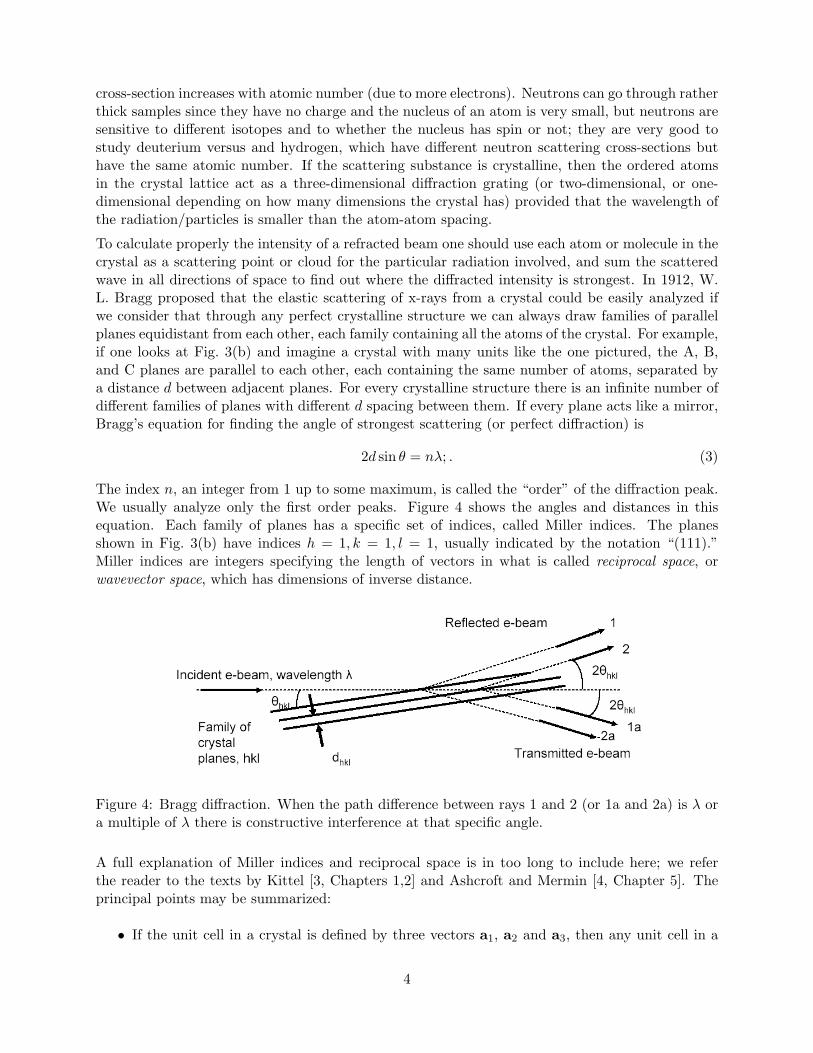
To calculate properly the intensity of a refracted beam one should use each atom or molecule in thecrystal as a scattering point or cloud for the particular radiation involved, and sum the scatteredwave in all directions of space to find out where the diffracted intensity is strongest. In 1912, W.L. Bragg proposed that the elastic scattering of x-rays from a crystal could be easily analyzed ifwe consider that through any perfect crystalline structure we can always draw families of parallelplanes equidistant from each other, each family containing all the atoms of the crystal. For example,if one looks at Fig. 3(b) and imagine a crystal with many units like the one pictured, the A, B,and C planes are parallel to each other, each containing the same number of atoms, separated bya distance d between adjacent planes. For every crystalline structure there is an infinite number ofdifferent families of planes with different d spacing between them. If every plane acts like a mirror,Bragg’s equation for finding the angle of strongest scattering (or perfect diffraction) is
2d sin θ = nλ; . (3)
The index n, an integer from 1 up to some maximum, is called the “order” of the diffraction peak.We usually analyze only the first order peaks. Figure 4 shows the angles and distances in thisequation. Each family of planes has a specific set of indices, called Miller indices. The planesshown in Fig. 3(b) have indices h = 1, k = 1, l = 1, usually indicated by the notation “(111).”Miller indices are integers specifying the length of vectors in what is called reciprocal space, orwavevector space, which has dimensions of inverse distance.
Figure 4: Bragg diffraction. When the path difference between rays 1 and 2 (or 1a and 2a) is λ ora multiple of λ there is constructive interference at that specific angle.
A full explanation of Miller indices and reciprocal space is in too long to include here; we referthe reader to the texts by Kittel [3, Chapters 1,2] and Ashcroft and Mermin [4, Chapter 5]. Theprincipal points may be summarized:
• If the unit cell in a crystal is defined by three vectors a1, a2 and a3, then any unit cell in a
4
crystal can be specified by a vector R = n1a1 + n2a2 + n3a3, where n1, n2, n3 are integers.The set of vectors {R} is the “real space lattice.”
• For the set of vectors {R} there is another set of vectors {K} such that eiK·R = 1. The set ofvectors {K} is called the “reciprocal space lattice.” Reciprocal space is also called “k-space,”“momentum space,” or “wavevector space.” It has the units of inverse length.
• Any K that satisfies the above conditions may be written as K = k1b1 + k2b2 + k3b3 wherek1, k2, k3 are integers and b1, b2, b3 are vectors that define the unit cell in reciprocal space.
• For any family of planes in the real space lattice separated by a distance d, the shortestreciprocal space vector has a direction that is perpendicular to these planes with a magnitudeof 2π/d. This vector may be written K = hb1 + kb2 + lb3. The integers h, k, l are the Millerindices which specify this particular reciprocal space vector.
In Fig. 4 we show an incident beam of radiation of wavelength λ, scattered or transmitted from afamily of parallel planes separated by dhkl. The reflected radiation direction is shown by rays 1 and2, and the transmitted radiation direction by rays 1a and 2a. The angle of incidence on a particularfamily of planes is θhkl, measured with respect to the lattice planes (not the incident beam directionas is done in 1-dimensional diffraction in optics). There is a reflected beam at angle 2θhkl withrespect to the incident beam direction, and also a transmitted beam at angle −2θhkl if there isnot strong attenuation through the crystal (or index of refraction change that would deviate thediffracted beam). With the construction shown in Fig. 4 it is easy to derive Bragg’s law.
Exercise 1 The kind of scattering assumed by Bragg’s law is elastic scattering, wherein the energyof the scattered radiation is the same as the energy of the incident radiation. This implies that thewavelength of the radiation does not change after it is scattered by the crystal. We can define awavevector k associated with a radiation beam as having a magnitude k = 2π/λ and a directionequal to the direction of the radiation. With this in mind,
1. Derive Bragg’s law from the geometry shown in Fig. 4. Remember that the condition forconstructive interference is that the path lengths followed by the interfering waves must differby integer multiples of the wavelength.
2. Show that de Broglie’s relation can be written in vector form as p = hk.
3. Let the wavevector of the incident e-beam in Fig. 4 be ki and the wavevector of the reflectede-beam be kr. These wavevectors have the same magnitude. Show by geometric constructionthat Bragg’s law is satisfied when kr − ki = K where K is a vector whose magnitude is2π/dhkl and whose direction is perpendicular to the family of planes specified by the Millerindices h, k, l. This shows that the reciprocal lattice {K} is the set of points that satisfy Bragg’slaw.
Exercise 2 The diffraction condition in a lattice may be expressed as H · R = integer, where thevector H = n/d, with n as the unit normal to the set of Bragg planes and d the spacing between them.The vector R is a translation vector in the lattice. For a simple cubic lattice, the translation vectoris a linear combination of a1 = [a, 0, 0], a2 = [0, a, 0], and a3 = [0, 0, a], so that R = a[n1, n2, n3],where ni is an integer. Show that the vector H = [h, k, l]/a with d = a/
√h2 + k2 + l2 satisfies
H ·R = integer in a simple cubic lattice for all integers h, k, l, with the vector [h, k, l] perpendicularto the Bragg plane. Note: K = 2πH.
5
There is a very large number of parallel equidistant planes in a macroscopic crystal (thousands),thus at the angle of constructive interference there is in-phase addition of wave amplitudes and theintensity is proportional to the square of the amplitude. If the angle is not “perfect” then thereis almost complete cancellation of the amplitude due to phase differences between rays and theintensity is practically zero. There is another reason why the intensity may be zero in a particulardirection, even if Bragg’s equation says that the interference should be constructive: the placementof atoms in the crystal plane is important, thus there may be crystal structures in which the reflectedintensity from atoms in one plane may be 180◦ out of phase with the one of the next parallel plane.If this occurs, then intensity in that specific direction is zero. This leads to atomic form factors andlattice structure factors and allowed and disallowed Miller indices when identifying a diffractionpattern.
The Bragg equation using Miller indices and our electron diffraction apparatus
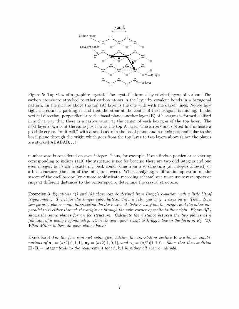
The samples in the four quadrants of the sample holder shown in Fig. 1 are either graphite oraluminum. Graphite crystallizes in a structure that resembles Fig. 3(c) with important differences,as noted in Fig. 5: it does not have all of the close packed atoms in each crystal plane A (or B).Instead, the carbon atoms are tied together with covalent bonds forming hexagons, so graphite is“missing” the center atom of Fig. 3(c). Also the c-axis (vertical, from one plane to the next) ismuch longer in graphite than for a close packed structure since the bonding between the A and Blayers is due to much weaker “van der Waals” forces (fluctuating electric dipoles), rather than thestrong covalent bonds that tie the atoms into hexagonal nets. The strong cohesion in the A (orB) planes and the very weak cohesion between planes A and B is what makes graphite so good asa lubricant and the reason why one can fabricate nowadays one-atomic-layer carbon films (calledgraphene).
For graphite, the scattering we observe is from the basal plane atoms and Bragg’s equation takesthe form
sin θhkl =√
h2 + hk + k2
(
λ√3 a
)
, (4)
where a is the magnitude of the unit cell base, 2.46 A= 0.246 nm, formed by the equal length “realspace” vectors a and b. One can complete the three-dimensional unit cell by drawing a vector c
perpendicular the plane of a and b, such that its length c is the repeat distance of the A planes.This cell is orthorhombic, with four carbon atoms per unit cell. (Can you draw the rest of the unitcell and check that there are four atoms in the cell?). All integer h and k are allowed values, withthe index l = 0.
For cubic structures, Bragg’s equation can be written
sin θhkl =√
h2 + k2 + l2(
λ
2a
)
. (5)
Here a is the side of the cube. There are specific rules that govern the allowed values of h, k, l dueto the fact that the common cubic structures have a basis (not just an atom at a corner) and thusa crystal structure factor which creates phase cancellation for scattering from some planes: for sclattices, h, k, and l can be any integer from 1 up until sin θhkl exceeds one (since there is no basis).For fcc lattices the (hkl) integers must be either all odd or all even. Another cubic lattice is bodycentered cubic or “bcc,” which is like simple cubic but with an additional atom located at the centerof the cubic unit cell. In this lattice, all integers are possible but their sum must be even. The
6
2.46 A
ab
A layer
B layer
Covalent bonds
Carbon atoms
Figure 5: Top view of a graphite crystal. The crystal is formed by stacked layers of carbon. Thecarbon atoms are attached to other carbon atoms in the layer by covalent bonds in a hexagonalpattern. In the picture above the top (A) layer is the one with with the darker lines. Notice howtight the covalent packing is, and that the atom at the center of the hexagons is missing. In thevertical direction, perpendicular to the basal plane, another layer (B) of hexagons is formed, shiftedin such a way that there is a carbon atom at the center of each hexagon of the top layer. Thenext layer down is at the same position as the top A layer. The arrows and dotted line indicate apossible crystal “unit cell,” with a and b axes in the basal plane, and a c axis perpendicular to thebasal plane through the origin which goes from the top layer to two layers above (since the planesare stacked ABABAB. . . ).
number zero is considered an even integer. Thus, for example, if one finds a particular scatteringcorresponding to indices (110) the structure is not fcc because there are two odd integers and oneeven integer, but such a scattering peak could come from a sc structure (all integers allowed) ora bcc structure (the sum of the integers is even). When analyzing a diffraction spectrum on thescreen of the oscilloscope (or a more sophisticate recording scheme) one must use several spots orrings at different distances to the center spot to determine the crystal structure.
Exercise 3 Equations (4) and (5) above can be derived from Bragg’s equation with a little bit oftrigonometry. Try it for the simple cubic lattice: draw a cube, put x, y, z axes on it. Then, drawtwo parallel planes—one intersecting the three axes at distances a from the origin and the other oneparallel to it either through the origin or through the cube corner opposite to the origin. Figure 3(b)shows the same planes for an fcc structure. Calculate the distance between the two planes as afunction of a using trigonometry. Then compare your result to Bragg’s law in the form of Eq. (5).What Miller indices do your planes have?
Exercise 4 For the face-centered cubic (fcc) lattice, the translation vectors R are linear combi-nations of a1 = (a/2)[0, 1, 1], a2 = (a/2)[1, 0, 1], and a3 = (a/2)[1, 1, 0]. Show that the conditionH · R = integer leads to the requirement that h, k, l be either all even or all odd.
7
4 The Experiment
In our apparatus the graphite sample is composed of a collection of mostly-oriented crystallinematerial with its c axis parallel to the electron beam. Since many regions are mostly oriented, witheffort one can obtain superimposed sets of diffraction “spots” which clearly show the hexagonalsymmetry of the carbon-net planes.
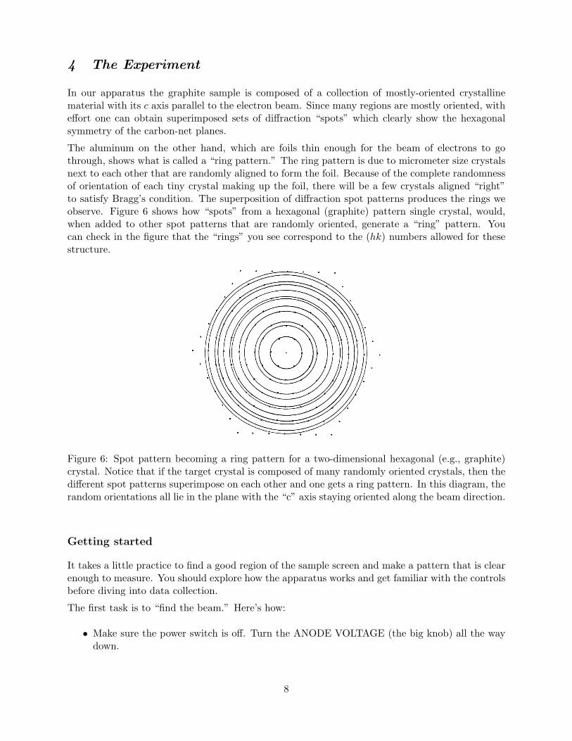
The aluminum on the other hand, which are foils thin enough for the beam of electrons to gothrough, shows what is called a “ring pattern.” The ring pattern is due to micrometer size crystalsnext to each other that are randomly aligned to form the foil. Because of the complete randomnessof orientation of each tiny crystal making up the foil, there will be a few crystals aligned “right”to satisfy Bragg’s condition. The superposition of diffraction spot patterns produces the rings weobserve. Figure 6 shows how “spots” from a hexagonal (graphite) pattern single crystal, would,when added to other spot patterns that are randomly oriented, generate a “ring” pattern. Youcan check in the figure that the “rings” you see correspond to the (hk) numbers allowed for thesestructure.
Figure 6: Spot pattern becoming a ring pattern for a two-dimensional hexagonal (e.g., graphite)crystal. Notice that if the target crystal is composed of many randomly oriented crystals, then thedifferent spot patterns superimpose on each other and one gets a ring pattern. In this diagram, therandom orientations all lie in the plane with the “c” axis staying oriented along the beam direction.
Getting started
It takes a little practice to find a good region of the sample screen and make a pattern that is clearenough to measure. You should explore how the apparatus works and get familiar with the controlsbefore diving into data collection.
The first task is to “find the beam.” Here’s how:
• Make sure the power switch is off. Turn the ANODE VOLTAGE (the big knob) all the waydown.
8
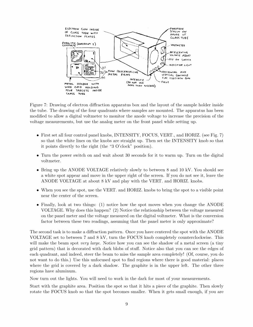
Figure 7: Drawing of electron diffraction apparatus box and the layout of the sample holder insidethe tube. The drawing of the four quadrants where samples are mounted. The apparatus has beenmodified to allow a digital voltmeter to monitor the anode voltage to increase the precision of thevoltage measurements, but use the analog meter on the front panel while setting up.
• First set all four control panel knobs, INTENSITY, FOCUS, VERT., and HORIZ. (see Fig. 7)so that the white lines on the knobs are straight up. Then set the INTENSITY knob so thatit points directly to the right (the “3 O’clock” position).
• Turn the power switch on and wait about 30 seconds for it to warm up. Turn on the digitalvoltmeter.
• Bring up the ANODE VOLTAGE relatively slowly to between 8 and 10 kV. You should seea white spot appear and move in the upper right of the screen. If you do not see it, leave theANODE VOLTAGE at about 8 kV and play with the VERT. and HORIZ. knobs.
• When you see the spot, use the VERT. and HORIZ. knobs to bring the spot to a visible pointnear the center of the screen.
• Finally, look at two things: (1) notice how the spot moves when you change the ANODEVOLTAGE. Why does this happen? (2) Notice the relationship between the voltage measuredon the panel meter and the voltage measured on the digital voltmeter. What is the conversionfactor between these two readings, assuming that the panel meter is only approximate?
The second task is to make a diffraction pattern. Once you have centered the spot with the ANODEVOLTAGE set to between 7 and 8 kV, turn the FOCUS knob completely counterclockwise. Thiswill make the beam spot very large. Notice how you can see the shadow of a metal screen (a tinygrid pattern) that is decorated with dark blobs of stuff. Notice also that you can see the edges ofeach quadrant, and indeed, steer the beam to miss the sample area completely! (Of, course, you donot want to do this.) Use this unfocused spot to find regions where there is good material: placeswhere the grid is covered by a dark shadow. The graphite is in the upper left. The other threeregions have aluminum.
Now turn out the lights. You will need to work in the dark for most of your measurements.
Start with the graphite area. Position the spot so that it hits a piece of the graphite. Then slowlyrotate the FOCUS knob so that the spot becomes smaller. When it gets small enough, if you are
9
lucky, you will see speckled rings appear, and you may be able to see spot patterns within therings that show six-fold symmetry. If you do not see such a pattern right away, play with the beamposition controls HORIZ. and VERT. and the FOCUS. Small adjustments can have a big effect!
Taking measurements
Before taking measurements please follow these precautions:
• Keep the INTENSITY as low as possible. If the beam intensity is high, the electronbeam may damage both the sample itself and the phosphor screen. You will notice thatthere are small dark patches on the screen: this is where the beam has burned the phosphorcoating.
• Turn the INTENSITY and ANODE VOLTAGE all the way down when you are
not actively taking data. As in the above, you want to avoid heating the phosphor screenand sample as much as possible.
Part 1: Graphite and de Broglie’s relationship
In this first part, you will study the relationship between the voltage measured by the voltmeter(digital and/or analog) and the diameter of one set of “spots” or “rings” of the graphite pattern.
First, locate a reasonably bright pattern at about 8 kV anode voltage. Then defocus the beam soyou can see what the sample looks like and where it is in the graphite quadrant. This will help youfind your sample as you change the anode voltage.
Before you start to collect data, see how low you can set the anode voltage and still find a pattern.Notice how sensitive the beam position is to the accelerating voltage. You will also notice that thelocation of the sample as seen on the screen will vary with voltage. Typically the minimum usefulvoltage is around 4 kV. (Higher voltages are easier.)
Then, starting from your minimum, record ring diameters D (or spot to spot distances, passingthrough the center) as a function of the anode voltage V for the first two rings. These are the {10}and {11} diffractions. (A note on notation conventions: when the Miller indices are enclosed insimple parens, like “(10),” this denotes a specific set of Miller indices, that is a specific set of crystalplanes; when the indices are enclosed in square brackets, like “[10],” this denotes a direction thatis perpendicular to those planes, that is, the direction of the reciprocal lattice vector associatedwith the Miller indices; when the indices are enclosed in curly brackets, like “{10},” this denotesa family of planes that all have the same spacing, that is, all of the diffraction spots that have thesame distance from the origin.)
Use the plastic calipers to measure distances directly from the screen. You should be able tomeasure to a precision of 0.1 mm using the vernier scale. Record the voltage from the digitalvoltmeter, and note how much variation there is in the reading. Make a table of D vs. V . Youshould be able to convert D into sin θhkl given that the distance L between the graphite sampleand the screen is 18.06 cm (as specified by the manufacturer). Ask yourself: am I measuring θhkl
or 2θhkl? Am I measuring the sine or the tangent of the angle? Calculate λ as a function of Vusing the proper Miller indices for the spot or ring you chose from Eq. (4) and the known spacinga. Make a plot based on combining the de Broglie relation, Eq. (1), and the energy relation, Eq. (2)that gives a straight line. The slope of this graph should give a relationship between fundamental
10
constants. Is your measurement right? Calculate possible sources of error and make a reasonableestimate of them. Note: if you are “orders of magnitude” off, check your units! This experimentworks well, with some care, to within 5% of the expected result.
Exercise 5 In this experiment, you are basically finding a relationship between accelerating po-tential V and the ratio of the electron wavelength λ to the lattice parameter d. Can you use thisapparatus to extract λ, the d value for aluminum and the d value for graphite without knowing oneof them a priori? If so, how might you do this? If not, how might you alter the experiment and/oruse other easily measured information to do so?
Part 2: Aluminum structure determination
The object of the second set of measurements is to determine the structure of the polycrystallinealuminum foil (sc, fcc or bcc). Use the same procedure as above to locate a good sample area:Defocus the beam, locate a region where the grid is covered with the foil sample, then refocus thebeam to see the diffraction pattern. Here you will see a set of unequally-spaced rings, similar tothose shown in Fig. 2 (although the contrast will not be as sharp).
Find a good “ring” pattern for a given ANODE VOLTAGE, FOCUS and INTENSITY. Then makea sketch of the ring pattern showing at least 5 rings (more if you can see them), and number therings in your sketch to keep track of them.
Then make a table that gives the ring diameters D (with uncertainty) versus ring number. Repeatthe measurements for a few different ANODE VOLTAGE settings (five voltages, reasonably spaced,is good).
To analyze these results, there are two things you want to find: the type of structure of thealuminum, which depends on the crystal structure factor and the length a of the lattice vector.
To determine the structure, first convert your D measurements into sin θ values, as you did earlier.Then choose one set corresponding to a particular anode voltage and plot these values versus√
h2 + k2 + l2 for the allowed Miller indices for the three different types of cubic structures. Youshould have three data sets on your plot, one for simple cubic (which allows all combinations ofintegers), one for face-centered cubic (in which only indices that are all odd or all even are allowed)and one for body-centered cubic (in which the sum of the indices must be an even number). Onlyone of these data sets will lie on a straight line: the one corresponding to the correct structure.
For example, to test simple cubic, if you labeled your rings 1, 2, 3,. . . starting from the innermostring, and then you found sin θ1, sin θ2, sin θ3,. . . , you would then plot these values versus 1 =√
12 + 02 + 02,√
2 =√
12 + 12 + 02,√
3 =√
12 + 12 + 12, . . . But for the other structures, somecombinations are not allowed, and the associations in your plot between your measurements and√
h2 + k2 + l2 would be different.
Exercise 6 Generate the ratio of the largest value of dhkl/a to the next 10 largest values of thesame quantity for graphite and the three cubic lattices (all h, k, l for simple cubic, h, k, l all even orall odd for fcc and the sum h + k + l is even for bcc). Use this for your analysis in Part 2. (Hint:use a spreadsheet.)
Once you have found the correct structure, fit that data to a line and extract the slope, whichwill be a function of λ and a. Repeat the analysis using the same structure for your other anode
11
voltages. Finally, plot these slopes as a function of λ, and extract a from a line fit, along with itsuncertainty.
Compare your result with a handbook value for aluminum. (You will need to look this up.)
References
[1] Tipler, Paul A. and Gene Mosca, Physics for Scientists and Engineers (Freeman, New York,2008).
[2] Chinn, M. D, and S. C. Fain, Jr., Journal of Vacuum Science and Technology, Volume 14, page314 (1977).
[3] Kittel, Charles, Introduction to Solid State Physics, sixth edition (Wiley, New York, 1986).
[4] Ashcroft, Neil W. and N. David Mermin, Solid State Physics (Saunders College, Philadelphia,1976).
Prepared by O. E. Vilches, D. B. Pengra, S. C. Fain, Jr., M. Olmstead,L. B. Sorensen, and J. Stoltenberg
electron_diffraction.tex -- Updated 12 July 2016
12


![Untitled-13 [courses.washington.edu]courses.washington.edu/nutr526/resources/ADAPregnancy.pdfTitle: Untitled-13 Created Date: 00000000000000Z](https://img.pdfslide.us/doc/110x75/5f7a5c71aa90ec1a0e56ce5a/-untitled-13-title-untitled-13-created-date-00000000000000z.jpg)