Embed Size (px)
Citation preview

Journal of Physics Conference Series
OPEN ACCESS
LiGA Research and Service at CAMDTo cite this article Jost Goettert et al 2006 J Phys Conf Ser 34 151
View the article online for updates and enhancements
You may also likeMultinary wurtzite-type oxidesemiconductors present status andperspectivesIssei Suzuki and Takahisa Omata
-
Recent studies of nonlinear chalcogenidecrystals for the mid-IRL I Isaenko and A P Yelisseyev
-
Wurtzite-derived ternary IndashIIIndashO2semiconductorsTakahisa Omata Hiraku Nagatani IsseiSuzuki et al
-
Recent citationsIntegration of rotated 3-D structures intopre-patterned PMMA substrate using stepamp stamp nanoimprint lithographyT Haatainen et al
-
Development of copper meshes forfrequency and spatial selection of theterahertz radiation of the Novosibirsk freeelectron laserS A Kuznetsov et al
-
Microelectromechanical systemassembled ion optics An advance tominiaturization and assembly of electronand ion opticsJ Fox et al
-
This content was downloaded from IP address 218102149202 on 29122021 at 1325
LiGA Research and Service at CAMD
Jost Goettert Proyag Datta Yohannes Desta Yoonyoung Jin Zhong-geng Ling Varshni Singh
Louisiana State University Center for Advaced Microstructures and Devices (CAMD) Jefferson Hwy Baton Rouge LA 70806 USA
jostlsuedu
Abstract Since 1995 CAMD has been offering exposure services so called print shop for a variety of users interested in making precision High-Aspect-Ratio Microstructures (HARMST) for various application Services have been expanded beyond only the print shop service in recent years and now include x-ray mask fabrication substrate preparation for PMMA and SU-8 resists electroplating finishing and molding Metallic and polymeric parts are now routinely fabricated for precision engineering micro-fluidic and micro-optic applications This paper presents a brief overview of the actual status of LiGA services provided at CAMD including ongoing research efforts and examples of LiGA components for different applications
1 Introduction The recently held HARMST 2005[1] Conference in Geongju South Korea presented many technical papers from groups worldwide related to LiGA based research efforts new processing capabilities and applications These contributions also included details on new equipment and fabrication capabilities demonstrating a strong interest from industrial users to consider LiGA technology for their applications and products
In the past years efforts at CAMD have been focused on providing new process capabilities including making taller (millimeter and higher) structures structures with sub-micrometer features 3D patterning better X-ray masks and use of advanced materials Besides RampD efforts in these areas the group has also established a LiGA service offering their skills to external customers and satisfying their needs for precision engineering parts and innovative high-tech products CAMD collaborates with a number of small start-up companies[234] who cannot afford to make multi-million dollar investments into infrastructure yet have a strong need for LiGA lsquoservicersquo and lsquopartnershiprsquo
Since its inception the LiGA process has impressed potential users with the outstanding precision tight tolerance high aspect ratio flexible 25 dimensional design sub-micrometer feature size smooth and vertical sidewalls and wide material choices These unique characteristics of LiGA structures provide component and system designers with a wide selection of material properties and flexible geometry for their applications Aspect ratios (defined as the ratio of structure height to smallest lateral dimensions) of 20-30 are typically patterned for lsquofree-standingrsquo microstructures and sub-micrometer features are successfully patterned when being part of a larger structure It should also be noted that even millimeter tall structures demonstrate extremely high precision with typical surface roughness of 20-50 nm Ra value and deviation from a perfectly straight sidewall of approximately 1 microm per 1 mm structure height[5] Besides fabrication of simple cylindrical structures more complex shapes including multi-level[6] and ldquoquasi 3Drdquo pattern as well as taller[7] (millimeter and higher) and
Institute of Physics Publishing Journal of Physics Conference Series 34 (2006) 912ndash918doi1010881742-6596341151 International MEMS Conference 2006
912copy 2006 IOP Publishing Ltd
smaller[8] (sub-micrometer) HARM structures are also patterned routinely as shown in Figs 1a-e In this paper we will briefly describe the LiGA service capabilities available at CAMD and show some examples of internal and external applications
Fig 1a ~ 25 mm tall gear patterned into PMMA resist[5]
Fig 1b 3 mm tall SU-8 posts with ~300 microm gaps[7]
Fig 1c 50 microm tall fluidic channels with ~ 5 microm wide post arrays
Fig 1d Conical posts in SU-8 made by 6x tilted and rotated exposures in 1 mm thick SU-8[9]
Fig 1e 3-level processed 15mm tall SU-8 micro-engine housing fabricated by combined optical and x-ray lithography[6]
2 X-ray Lithography Service and New Process Capabilities at CAMD CAMD operates four micromachining beamlines equipped with different scanners providing
patterning solutions including aligned tilted and rotated exposures as well as multiple- andor large substrate formats needed for high throughput exposures Light is provided from bending magnets to three of the beamlines (critical energy = 16 keV) while a 7-Tesla wiggler provides hard x-rays (critical energy = 795 keV) for UDXRL exposures at one port[10] Over the last years CAMD has exposed more than 650 substrates per year for a number of users Approximately 13 of these substrates are from industrial users indicating a strong interest in the exposure capabilities offered[11] In the past year (2005) the number of industry user substrates increased to 40 demonstrating a growing interest There was also a significant increase (gt 50 ) of accumulated exposure dose from 134 x 107 mAmiddotmin in 2004 to 2105 x 107 mAmiddotmin in 2005 showing the need for exposing thick resist layers as well as larger areas This accumulated exposure dose and thus fabrication costs could be significantly reduced if the primarily used PMMA resist could be replaced with SU-8 which still suffers from a lack of process stability and repeatability
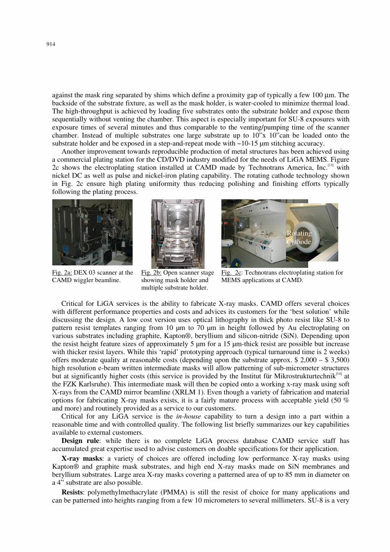
New process capabilities are shown in Figs 2a-c A lsquohigher throughputrsquo scanner (DEX 03 from Jenoptik GmbH[12] Germany) financially supported through a DARPA grant (grant N66001ndash00ndash8968) and designed and engineered by Jenoptik GmbH Germany according to specifications from CAMD researchers Figure 2b shows the open flap of the DEX 03 scanner The mask is mounted to a mask holder sitting on the Y-scanning stage Up to five 4rdquo wafer substrates are pressed sequentially
913
against the mask ring separated by shims which define a proximity gap of typically a few 100 μm The backside of the substrate fixture as well as the mask holder is water-cooled to minimize thermal load The high-throughput is achieved by loading five substrates onto the substrate holder and expose them sequentially without venting the chamber This aspect is especially important for SU-8 exposures with exposure times of several minutes and thus comparable to the ventingpumping time of the scanner chamber Instead of multiple substrates one large substrate up to 10rdquox 10rdquocan be loaded onto the substrate holder and be exposed in a step-and-repeat mode with ~10-15 microm stitching accuracy
Another improvement towards reproducible production of metal structures has been achieved using a commercial plating station for the CDDVD industry modified for the needs of LiGA MEMS Figure 2c shows the electroplating station installed at CAMD made by Technotrans America Inc[13] with nickel DC as well as pulse and nickel-iron plating capability The rotating cathode technology shown in Fig 2c ensure high plating uniformity thus reducing polishing and finishing efforts typically following the plating process
Fig 2a DEX 03 scanner at the CAMD wiggler beamline
Fig 2b Open scanner stage showing mask holder and multiple substrate holder
Fig 2c Technotrans electroplating station for MEMS applications at CAMD
Critical for LiGA services is the ability to fabricate X-ray masks CAMD offers several choices
with different performance properties and costs and advices its customers for the lsquobest solutionrsquo while discussing the design A low cost version uses optical lithography in thick photo resist like SU-8 to pattern resist templates ranging from 10 microm to 70 microm in height followed by Au electroplating on various substrates including graphite Kaptonreg beryllium and silicon-nitride (SiN) Depending upon the resist height feature sizes of approximately 5 microm for a 15 microm-thick resist are possible but increase with thicker resist layers While this lsquorapidrsquo prototyping approach (typical turnaround time is 2 weeks) offers moderate quality at reasonable costs (depending upon the substrate approx $ 2000 ndash $ 3500) high resolution e-beam written intermediate masks will allow patterning of sub-micrometer structures but at significantly higher costs (this service is provided by the Institut fuumlr Mikrostrukturtechnik[14] at the FZK Karlsruhe) This intermediate mask will then be copied onto a working x-ray mask using soft X-rays from the CAMD mirror beamline (XRLM 1) Even though a variety of fabrication and material options for fabricating X-ray masks exists it is a fairly mature process with acceptable yield (50 and more) and routinely provided as a service to our customers
Critical for any LiGA service is the in-house capability to turn a design into a part within a reasonable time and with controlled quality The following list briefly summarizes our key capabilities available to external customers
Design rule while there is no complete LiGA process database CAMD service staff has accumulated great expertise used to advise customers on doable specifications for their application
X-ray masks a variety of choices are offered including low performance X-ray masks using Kaptonreg and graphite mask substrates and high end X-ray masks made on SiN membranes and beryllium substrates Large area X-ray masks covering a patterned area of up to 85 mm in diameter on a 4rdquo substrate are also possible
Resists polymethylmethacrylate (PMMA) is still the resist of choice for many applications and can be patterned into heights ranging from a few 10 micrometers to several millimeters SU-8 is a very
Rotating Cathode
914
attractive resist alternative but still lacks stable process parameters especially for thicker layers (500 microm and higher) CAMD also provides resist coated substrates as a service
Exposure Service LiGA print-shop services allow customers to submit exposure requests with CAMD experts performing the service Special customer mask and substrate format can be accommodated even though the CAMD standard formats are preferred
Sample developing CAMD provides developing services using beaker-type setups with magnetic stirring and cyclic development for minimum exposure of the resist to the developer solution
Electroplating a variety of plating baths including nickel nickel-iron alloy copper and gold are available for plating into LiGA substrates or other customer-provided resist templates
Polishing and finishing surface finishing of metal structures is achieved by lapping and polishing with typical roughness of less than 1 microm Ra value and height control of +- 5 microm
Molding CAMD offers molding services including mold insert fabrication and small scale replication in commonly used polymers like PMMA PC and COC Molding of new materials will be provided as development service
3 Examples of Research and Applications
31 Materials Research Polymer nano-composites (PNCs) have in the past decade emerged as a new class of materials due to much improved mechanical thermal electrical and optical properties as compared to their macro- and micro-composites[1516] However there is the challenge in the integration of multi-functional PNC components into micro-electro-mechanical systems (MEMS) CAMD researchers use epoxy resist (SU-8 5) with carbon black powder filler (2-15 wt) in combination with x-ray lithography to pattern conductive resist materials Figure 3a and b show some first structures patterned with a bottom dose of 10 mJcm3 using a graphite X-ray mask A high load of 15 wt of carbon black in the resist material yielded an average elastic modulus of 15 GPa nearly five times that of pure SU-8
Ni-Fe alloy is a potential material to replace Ni for specific applications such as high strength microstructures high temperature mold insert or microstructures with magnetic property based applications Figure 3c illustrates the current capabilities in Ni-Fe alloy electroplating of the CAMDLSU service group Electroplating was performed using a plating bath prepared by mixing nickel sulfate and iron sulfate Ni-Fe alloy with Fe content of 15 producing a hardness of 690 HK025N with a high wear resistance can be plated with a plating rate gt20 micromhr The high material uniformity across a 1mm tall structure has been measured using the EDS feature of the SEM The SEM picture illustrates that the quality of deposition is comparable to Ni electroplated structures
Fig 3ab Preliminary PNC structures (SU-8 resist with carbon black) patterned by x-ray lithography
Fig 3c SEM image of microgear with EDS results of NiFe alloy with 15 Fe
Fe 1499 Fe 1541 Fe 1537
Fe 1448 Fe 1511
100 microm
Support substrate
PNC sidewall PNC top
surface
130 microm
43 microm
915
32 Polymer chips for BioMEMS applications CAMD offers molding services including mold insert fabrication and small scale replication in commonly used polymers like PMMA PC and COC Molding is one of the paths to mass production of high aspect ratio microstructures Mold inserts are fabricated using X-ray LiGA SU-8 LiGA and direct micromilling of brass Brass mold inserts do not possess the surface and sidewall roughness or the aspect ratios that can be achieved using a LiGA mold insert but they are useful as a rapid prototyping tool In collaboration with LSUrsquos Center for BioModular Multi-scale Systems[17] (CBM2) a number of fluidic chips for BioMEMS applications are routinely fabricated and combined to perform complex analytical protocols Some examples of inserts and molded chips are shown in Figs 4a-4d
Fig 4ab Brass (left) and LiGA Ni (right) mold inserts
Fig 4cd Examples of fluidic chips left shows a set of 1rdquox3rdquo chips to be combined for a fluidic stack[18] right shows a fluidic chip with integrated waveguide[19]
33 Examples of Applications from HT Micro Commercial applications for deep X-ray lithography based processing include several broad categories where the ability to batch fabricate precision high aspect-ratio geometry offers unique solutions
For many milliscale components the challenge that presents itself is how to maintain dimensional tolerances as well as minimum dimensions at reduced component size with materials suited for and compatible with a given application As an example biofluidic interfaces many times share these requirements Figure 5a shows a 4-layer plastic component comprised entirely of PMMA and fabricated with deep X-ray lithography Within this component are 12 channels that feed 12 reservoirs ldquocagedrdquo in by PMMA pillars as shown in the detail photographs in Fig 5b The PMMA cage structures consist of rows of 30 microm diameter cylindrical pillars with 300 microm height that reside on 33 microm centers resulting in rows of 3 x 300 microm gaps Another similar millimeter size bio interface structure with micron precision features is exhibited in Fig 5c This particular component also constructed with multi-layer PMMA contains features interfacing with three optical fibers This optical biosensor component consists of plastic layers that form a press-fit with the optical fiber
Another set of components springs combines precision patterning using deep X-ray lithography and electroplating of high yield strength materials such as NiFe alloys By precisely controlling the structure features a simple spring-mass acceleration switch may be realized as shown in Fig 5d The spiral spring supports a ring which when accelerated will contact the outer rim or top (not shown) and bottom shoulder at a predefined acceleration threshold
Fig 5ab PMMA Fluidic chips with integrated flow filter structures
Fig 5c Optical biosensor with fibers
Fig 5d NiFe acceleration switch
The ability to maintain tolerances between high aspect ratio structures also aids considerably in the ability to batch fabricate microactuators where a small (micron) working gap can be maintained
channel waveguide
waveguide chip
916
through relatively much larger thickness and overlap stroke dimensions of several hundred microns Coupled with compliant springs low frequency (20 Hz) resonators with several hundred micron amplitudes may be fabricated Such resonant actuators have been applied to generate structured light sources for use in miniature con-focal microscopes Figure 6a shows a microscope developed at the University of Arizona which uses a deep X-ray lithography defined ldquooptical benchrdquo for alignment and support of miniature optics as well as a resonant amplitude grating that provides structured light into the microscope when illuminated from a dc source[20 21] The amplitude grating is shown supported by the center of the resonant actuator in Fig 6b which also shows the electrostatic comb drive which is capable of resonating the grating at +- 100 microm amplitude with 10 Volts with quality factors at atmosphere of over 50 Figure 6c reveals a view of the left side of the microscope in Fig 6a where a conventional 1mm diameter glass objective lens is supported and clamped to the optical bench
Fig 6a-c Example of a micro-optical bench with integrated electrostatic actuator (see text for details)
4 Conclusions This paper briefly described the ongoing activities in LiGA research and service at CAMD The examples of applications in microfluidic micro-optic and precision engineering are mainly made possible by the unique patterning capabilities of the x-ray lithography process and the choices of materials in the electroplating and molding steps While lsquomanufacturingrsquo service with many hundreds or even thousands of parts remains a major challenge for the CAMD service group lsquoprototype productionrsquo of several ten prototypes with good yield and reasonable turnaround time is routinely provided and in growing demand also from industrial users
Acknowledgements The authors would like to thank their colleagues at CAMD as well as the CAMD student users for their support in developing new processes Special thanks to Todd Christenson from HT Micro for providing the many examples demonstrating the need and interest in LiGA microfabricated structures Funding is gratefully acknowledged from the State of Louisiana DARPA MTO NSF and NIH
References [1] Proceeding HARMST 2005 Geongju South Korea June 2005 Many of the abstracts included
in the proceedings will be published as reviewed papers in Microsystems Technologies in the near future
[2] Webpage Mezzo International httpwwwmezzotechbiz [3] Webpage Micromotion httpwwwmikrogetriebedesitesenglishabout-ushtml [4] Webpage HT Micro httpwwwhtmicrocom [5] Aigeldinger G ldquoImplementation of an Ultra Deep X-ray Lithography System at CAMDrdquo
PhD thesis University Freiburg 2001
917
[6] Jian L Desta YM Aigeldinger G Bednarzik M Goettert J Loechel B Jin Y Singh
V Ahrens G Gruetzner G Ruhmann R Degen R ldquoSU-8 based deep x-ray lithographyLIGArdquo Proc SPIE Vol 4979 2003 394-401
[7] Becnel C Desta Y and Kelly K Ultra-deep x-ray lithography of densely packed SU-8 features IampII An SU-8 casting procedure to obtain uniform solvent content with accompanying experimental results Journal of Micromechanics and Microengineering 2005(6) p 1242
[8] Wang L Desta YM Goettert J Ling Z Kong JR Aristone F Jin Y Christenson TR Bradshaw K ldquoHigh resolution x-ray masks for high aspect ratio microelectromechanical systems (HARMS)rdquo Proc SPIE Vol 4979 2003 p 508-513
[9] Details about beamlines and exposure spectra can be found on the CAMD webpage at httpwwwcamdlsuedubeamlines
[10] R Turner Y Desta K Kelly J Zhang E Geiger S Cortez D Mancini rdquoTapered LIGA HARMsrdquo J Micromech Microeng 13 (2003) pp 367-372
[11] More details on exposure services are available from CAMDrsquos Annual Reports on the CAMD homepage at httpwwwcamdlsuedu
[12] Webpage Jenoptik GmbH httpwwwjo-mikrotechnikcom [13] Webpage Technotrans GmbH httpwwwtechnotranscom [14] Webpage IMT httpwwwfzkdeimt [15] Technology Road Map (TRM) ndash Towards Commercialization of Nano-composites and
PolymerCeramic Hybrids The Faraday Plastics Partnership and HybridNet 2005 [16] Salahuddin N Moet A Hiltner A Baer E ldquoNanoscale Highly Filled Epoxy
Nanocompositerdquo European Polymer Journal Vol 38 2002 pp 1477-1482 [17] Webpage CBM2 httpwwwcbmmlsuedu [18] M Pease V Singh P Datta O Kizilkaya E Kornemann and J Goettert ldquoMicrofluidic
Labware forDeveloping Biofunctional Surface on GMR Sensorrdquo Book of Abstracts HARMST05 June 10-13 2005 Gyeongju Korea pp 94-95 2005 June 2005 submitted for publication to Microsystem Technologies
[19] Proyag Datta Feng Xu Sitanshu Gurung Steven A Soper and Jost Goettert ldquoPolymeric Waveguides for Orthogonal Near Surface Fluorescent Excitationldquo Microfluidics BioMEMS and Medical Microsystems IV from the Proceedings of SPIE Vol 6112 2006
[20] TS Tkaczyk JD Rogers M Rahman TC Christenson S Gaalema EL Dereniak R Richards-Kortum MR Descour ldquoMulti-modal miniature microscope 4M Device for bio-imaging applications ndash an overview of the systemldquo Proc SPIE Vol 5959 2005 pp 138-146
[21] JD Rogers A Kaumlrkkaumlinen TS Tkaczyk J Rantala and MR Descour ldquoRealization of refractive microoptics through grayscale lithographi patterning of photosensitive hybrid glassldquo Opt Express 12 2004 pp 1294-1303 httpwwwopticsinfobaseorgabstarctcfmURI=oe-12-7-1294
918

LiGA Research and Service at CAMD
Jost Goettert Proyag Datta Yohannes Desta Yoonyoung Jin Zhong-geng Ling Varshni Singh
Louisiana State University Center for Advaced Microstructures and Devices (CAMD) Jefferson Hwy Baton Rouge LA 70806 USA
jostlsuedu
Abstract Since 1995 CAMD has been offering exposure services so called print shop for a variety of users interested in making precision High-Aspect-Ratio Microstructures (HARMST) for various application Services have been expanded beyond only the print shop service in recent years and now include x-ray mask fabrication substrate preparation for PMMA and SU-8 resists electroplating finishing and molding Metallic and polymeric parts are now routinely fabricated for precision engineering micro-fluidic and micro-optic applications This paper presents a brief overview of the actual status of LiGA services provided at CAMD including ongoing research efforts and examples of LiGA components for different applications
1 Introduction The recently held HARMST 2005[1] Conference in Geongju South Korea presented many technical papers from groups worldwide related to LiGA based research efforts new processing capabilities and applications These contributions also included details on new equipment and fabrication capabilities demonstrating a strong interest from industrial users to consider LiGA technology for their applications and products
In the past years efforts at CAMD have been focused on providing new process capabilities including making taller (millimeter and higher) structures structures with sub-micrometer features 3D patterning better X-ray masks and use of advanced materials Besides RampD efforts in these areas the group has also established a LiGA service offering their skills to external customers and satisfying their needs for precision engineering parts and innovative high-tech products CAMD collaborates with a number of small start-up companies[234] who cannot afford to make multi-million dollar investments into infrastructure yet have a strong need for LiGA lsquoservicersquo and lsquopartnershiprsquo
Since its inception the LiGA process has impressed potential users with the outstanding precision tight tolerance high aspect ratio flexible 25 dimensional design sub-micrometer feature size smooth and vertical sidewalls and wide material choices These unique characteristics of LiGA structures provide component and system designers with a wide selection of material properties and flexible geometry for their applications Aspect ratios (defined as the ratio of structure height to smallest lateral dimensions) of 20-30 are typically patterned for lsquofree-standingrsquo microstructures and sub-micrometer features are successfully patterned when being part of a larger structure It should also be noted that even millimeter tall structures demonstrate extremely high precision with typical surface roughness of 20-50 nm Ra value and deviation from a perfectly straight sidewall of approximately 1 microm per 1 mm structure height[5] Besides fabrication of simple cylindrical structures more complex shapes including multi-level[6] and ldquoquasi 3Drdquo pattern as well as taller[7] (millimeter and higher) and
Institute of Physics Publishing Journal of Physics Conference Series 34 (2006) 912ndash918doi1010881742-6596341151 International MEMS Conference 2006
912copy 2006 IOP Publishing Ltd
smaller[8] (sub-micrometer) HARM structures are also patterned routinely as shown in Figs 1a-e In this paper we will briefly describe the LiGA service capabilities available at CAMD and show some examples of internal and external applications
Fig 1a ~ 25 mm tall gear patterned into PMMA resist[5]
Fig 1b 3 mm tall SU-8 posts with ~300 microm gaps[7]
Fig 1c 50 microm tall fluidic channels with ~ 5 microm wide post arrays
Fig 1d Conical posts in SU-8 made by 6x tilted and rotated exposures in 1 mm thick SU-8[9]
Fig 1e 3-level processed 15mm tall SU-8 micro-engine housing fabricated by combined optical and x-ray lithography[6]
2 X-ray Lithography Service and New Process Capabilities at CAMD CAMD operates four micromachining beamlines equipped with different scanners providing
patterning solutions including aligned tilted and rotated exposures as well as multiple- andor large substrate formats needed for high throughput exposures Light is provided from bending magnets to three of the beamlines (critical energy = 16 keV) while a 7-Tesla wiggler provides hard x-rays (critical energy = 795 keV) for UDXRL exposures at one port[10] Over the last years CAMD has exposed more than 650 substrates per year for a number of users Approximately 13 of these substrates are from industrial users indicating a strong interest in the exposure capabilities offered[11] In the past year (2005) the number of industry user substrates increased to 40 demonstrating a growing interest There was also a significant increase (gt 50 ) of accumulated exposure dose from 134 x 107 mAmiddotmin in 2004 to 2105 x 107 mAmiddotmin in 2005 showing the need for exposing thick resist layers as well as larger areas This accumulated exposure dose and thus fabrication costs could be significantly reduced if the primarily used PMMA resist could be replaced with SU-8 which still suffers from a lack of process stability and repeatability
New process capabilities are shown in Figs 2a-c A lsquohigher throughputrsquo scanner (DEX 03 from Jenoptik GmbH[12] Germany) financially supported through a DARPA grant (grant N66001ndash00ndash8968) and designed and engineered by Jenoptik GmbH Germany according to specifications from CAMD researchers Figure 2b shows the open flap of the DEX 03 scanner The mask is mounted to a mask holder sitting on the Y-scanning stage Up to five 4rdquo wafer substrates are pressed sequentially
913
against the mask ring separated by shims which define a proximity gap of typically a few 100 μm The backside of the substrate fixture as well as the mask holder is water-cooled to minimize thermal load The high-throughput is achieved by loading five substrates onto the substrate holder and expose them sequentially without venting the chamber This aspect is especially important for SU-8 exposures with exposure times of several minutes and thus comparable to the ventingpumping time of the scanner chamber Instead of multiple substrates one large substrate up to 10rdquox 10rdquocan be loaded onto the substrate holder and be exposed in a step-and-repeat mode with ~10-15 microm stitching accuracy
Another improvement towards reproducible production of metal structures has been achieved using a commercial plating station for the CDDVD industry modified for the needs of LiGA MEMS Figure 2c shows the electroplating station installed at CAMD made by Technotrans America Inc[13] with nickel DC as well as pulse and nickel-iron plating capability The rotating cathode technology shown in Fig 2c ensure high plating uniformity thus reducing polishing and finishing efforts typically following the plating process
Fig 2a DEX 03 scanner at the CAMD wiggler beamline
Fig 2b Open scanner stage showing mask holder and multiple substrate holder
Fig 2c Technotrans electroplating station for MEMS applications at CAMD
Critical for LiGA services is the ability to fabricate X-ray masks CAMD offers several choices
with different performance properties and costs and advices its customers for the lsquobest solutionrsquo while discussing the design A low cost version uses optical lithography in thick photo resist like SU-8 to pattern resist templates ranging from 10 microm to 70 microm in height followed by Au electroplating on various substrates including graphite Kaptonreg beryllium and silicon-nitride (SiN) Depending upon the resist height feature sizes of approximately 5 microm for a 15 microm-thick resist are possible but increase with thicker resist layers While this lsquorapidrsquo prototyping approach (typical turnaround time is 2 weeks) offers moderate quality at reasonable costs (depending upon the substrate approx $ 2000 ndash $ 3500) high resolution e-beam written intermediate masks will allow patterning of sub-micrometer structures but at significantly higher costs (this service is provided by the Institut fuumlr Mikrostrukturtechnik[14] at the FZK Karlsruhe) This intermediate mask will then be copied onto a working x-ray mask using soft X-rays from the CAMD mirror beamline (XRLM 1) Even though a variety of fabrication and material options for fabricating X-ray masks exists it is a fairly mature process with acceptable yield (50 and more) and routinely provided as a service to our customers
Critical for any LiGA service is the in-house capability to turn a design into a part within a reasonable time and with controlled quality The following list briefly summarizes our key capabilities available to external customers
Design rule while there is no complete LiGA process database CAMD service staff has accumulated great expertise used to advise customers on doable specifications for their application
X-ray masks a variety of choices are offered including low performance X-ray masks using Kaptonreg and graphite mask substrates and high end X-ray masks made on SiN membranes and beryllium substrates Large area X-ray masks covering a patterned area of up to 85 mm in diameter on a 4rdquo substrate are also possible
Resists polymethylmethacrylate (PMMA) is still the resist of choice for many applications and can be patterned into heights ranging from a few 10 micrometers to several millimeters SU-8 is a very
Rotating Cathode
914
attractive resist alternative but still lacks stable process parameters especially for thicker layers (500 microm and higher) CAMD also provides resist coated substrates as a service
Exposure Service LiGA print-shop services allow customers to submit exposure requests with CAMD experts performing the service Special customer mask and substrate format can be accommodated even though the CAMD standard formats are preferred
Sample developing CAMD provides developing services using beaker-type setups with magnetic stirring and cyclic development for minimum exposure of the resist to the developer solution
Electroplating a variety of plating baths including nickel nickel-iron alloy copper and gold are available for plating into LiGA substrates or other customer-provided resist templates
Polishing and finishing surface finishing of metal structures is achieved by lapping and polishing with typical roughness of less than 1 microm Ra value and height control of +- 5 microm
Molding CAMD offers molding services including mold insert fabrication and small scale replication in commonly used polymers like PMMA PC and COC Molding of new materials will be provided as development service
3 Examples of Research and Applications
31 Materials Research Polymer nano-composites (PNCs) have in the past decade emerged as a new class of materials due to much improved mechanical thermal electrical and optical properties as compared to their macro- and micro-composites[1516] However there is the challenge in the integration of multi-functional PNC components into micro-electro-mechanical systems (MEMS) CAMD researchers use epoxy resist (SU-8 5) with carbon black powder filler (2-15 wt) in combination with x-ray lithography to pattern conductive resist materials Figure 3a and b show some first structures patterned with a bottom dose of 10 mJcm3 using a graphite X-ray mask A high load of 15 wt of carbon black in the resist material yielded an average elastic modulus of 15 GPa nearly five times that of pure SU-8
Ni-Fe alloy is a potential material to replace Ni for specific applications such as high strength microstructures high temperature mold insert or microstructures with magnetic property based applications Figure 3c illustrates the current capabilities in Ni-Fe alloy electroplating of the CAMDLSU service group Electroplating was performed using a plating bath prepared by mixing nickel sulfate and iron sulfate Ni-Fe alloy with Fe content of 15 producing a hardness of 690 HK025N with a high wear resistance can be plated with a plating rate gt20 micromhr The high material uniformity across a 1mm tall structure has been measured using the EDS feature of the SEM The SEM picture illustrates that the quality of deposition is comparable to Ni electroplated structures
Fig 3ab Preliminary PNC structures (SU-8 resist with carbon black) patterned by x-ray lithography
Fig 3c SEM image of microgear with EDS results of NiFe alloy with 15 Fe
Fe 1499 Fe 1541 Fe 1537
Fe 1448 Fe 1511
100 microm
Support substrate
PNC sidewall PNC top
surface
130 microm
43 microm
915
32 Polymer chips for BioMEMS applications CAMD offers molding services including mold insert fabrication and small scale replication in commonly used polymers like PMMA PC and COC Molding is one of the paths to mass production of high aspect ratio microstructures Mold inserts are fabricated using X-ray LiGA SU-8 LiGA and direct micromilling of brass Brass mold inserts do not possess the surface and sidewall roughness or the aspect ratios that can be achieved using a LiGA mold insert but they are useful as a rapid prototyping tool In collaboration with LSUrsquos Center for BioModular Multi-scale Systems[17] (CBM2) a number of fluidic chips for BioMEMS applications are routinely fabricated and combined to perform complex analytical protocols Some examples of inserts and molded chips are shown in Figs 4a-4d
Fig 4ab Brass (left) and LiGA Ni (right) mold inserts
Fig 4cd Examples of fluidic chips left shows a set of 1rdquox3rdquo chips to be combined for a fluidic stack[18] right shows a fluidic chip with integrated waveguide[19]
33 Examples of Applications from HT Micro Commercial applications for deep X-ray lithography based processing include several broad categories where the ability to batch fabricate precision high aspect-ratio geometry offers unique solutions
For many milliscale components the challenge that presents itself is how to maintain dimensional tolerances as well as minimum dimensions at reduced component size with materials suited for and compatible with a given application As an example biofluidic interfaces many times share these requirements Figure 5a shows a 4-layer plastic component comprised entirely of PMMA and fabricated with deep X-ray lithography Within this component are 12 channels that feed 12 reservoirs ldquocagedrdquo in by PMMA pillars as shown in the detail photographs in Fig 5b The PMMA cage structures consist of rows of 30 microm diameter cylindrical pillars with 300 microm height that reside on 33 microm centers resulting in rows of 3 x 300 microm gaps Another similar millimeter size bio interface structure with micron precision features is exhibited in Fig 5c This particular component also constructed with multi-layer PMMA contains features interfacing with three optical fibers This optical biosensor component consists of plastic layers that form a press-fit with the optical fiber
Another set of components springs combines precision patterning using deep X-ray lithography and electroplating of high yield strength materials such as NiFe alloys By precisely controlling the structure features a simple spring-mass acceleration switch may be realized as shown in Fig 5d The spiral spring supports a ring which when accelerated will contact the outer rim or top (not shown) and bottom shoulder at a predefined acceleration threshold
Fig 5ab PMMA Fluidic chips with integrated flow filter structures
Fig 5c Optical biosensor with fibers
Fig 5d NiFe acceleration switch
The ability to maintain tolerances between high aspect ratio structures also aids considerably in the ability to batch fabricate microactuators where a small (micron) working gap can be maintained
channel waveguide
waveguide chip
916
through relatively much larger thickness and overlap stroke dimensions of several hundred microns Coupled with compliant springs low frequency (20 Hz) resonators with several hundred micron amplitudes may be fabricated Such resonant actuators have been applied to generate structured light sources for use in miniature con-focal microscopes Figure 6a shows a microscope developed at the University of Arizona which uses a deep X-ray lithography defined ldquooptical benchrdquo for alignment and support of miniature optics as well as a resonant amplitude grating that provides structured light into the microscope when illuminated from a dc source[20 21] The amplitude grating is shown supported by the center of the resonant actuator in Fig 6b which also shows the electrostatic comb drive which is capable of resonating the grating at +- 100 microm amplitude with 10 Volts with quality factors at atmosphere of over 50 Figure 6c reveals a view of the left side of the microscope in Fig 6a where a conventional 1mm diameter glass objective lens is supported and clamped to the optical bench
Fig 6a-c Example of a micro-optical bench with integrated electrostatic actuator (see text for details)
4 Conclusions This paper briefly described the ongoing activities in LiGA research and service at CAMD The examples of applications in microfluidic micro-optic and precision engineering are mainly made possible by the unique patterning capabilities of the x-ray lithography process and the choices of materials in the electroplating and molding steps While lsquomanufacturingrsquo service with many hundreds or even thousands of parts remains a major challenge for the CAMD service group lsquoprototype productionrsquo of several ten prototypes with good yield and reasonable turnaround time is routinely provided and in growing demand also from industrial users
Acknowledgements The authors would like to thank their colleagues at CAMD as well as the CAMD student users for their support in developing new processes Special thanks to Todd Christenson from HT Micro for providing the many examples demonstrating the need and interest in LiGA microfabricated structures Funding is gratefully acknowledged from the State of Louisiana DARPA MTO NSF and NIH
References [1] Proceeding HARMST 2005 Geongju South Korea June 2005 Many of the abstracts included
in the proceedings will be published as reviewed papers in Microsystems Technologies in the near future
[2] Webpage Mezzo International httpwwwmezzotechbiz [3] Webpage Micromotion httpwwwmikrogetriebedesitesenglishabout-ushtml [4] Webpage HT Micro httpwwwhtmicrocom [5] Aigeldinger G ldquoImplementation of an Ultra Deep X-ray Lithography System at CAMDrdquo
PhD thesis University Freiburg 2001
917
[6] Jian L Desta YM Aigeldinger G Bednarzik M Goettert J Loechel B Jin Y Singh
V Ahrens G Gruetzner G Ruhmann R Degen R ldquoSU-8 based deep x-ray lithographyLIGArdquo Proc SPIE Vol 4979 2003 394-401
[7] Becnel C Desta Y and Kelly K Ultra-deep x-ray lithography of densely packed SU-8 features IampII An SU-8 casting procedure to obtain uniform solvent content with accompanying experimental results Journal of Micromechanics and Microengineering 2005(6) p 1242
[8] Wang L Desta YM Goettert J Ling Z Kong JR Aristone F Jin Y Christenson TR Bradshaw K ldquoHigh resolution x-ray masks for high aspect ratio microelectromechanical systems (HARMS)rdquo Proc SPIE Vol 4979 2003 p 508-513
[9] Details about beamlines and exposure spectra can be found on the CAMD webpage at httpwwwcamdlsuedubeamlines
[10] R Turner Y Desta K Kelly J Zhang E Geiger S Cortez D Mancini rdquoTapered LIGA HARMsrdquo J Micromech Microeng 13 (2003) pp 367-372
[11] More details on exposure services are available from CAMDrsquos Annual Reports on the CAMD homepage at httpwwwcamdlsuedu
[12] Webpage Jenoptik GmbH httpwwwjo-mikrotechnikcom [13] Webpage Technotrans GmbH httpwwwtechnotranscom [14] Webpage IMT httpwwwfzkdeimt [15] Technology Road Map (TRM) ndash Towards Commercialization of Nano-composites and
PolymerCeramic Hybrids The Faraday Plastics Partnership and HybridNet 2005 [16] Salahuddin N Moet A Hiltner A Baer E ldquoNanoscale Highly Filled Epoxy
Nanocompositerdquo European Polymer Journal Vol 38 2002 pp 1477-1482 [17] Webpage CBM2 httpwwwcbmmlsuedu [18] M Pease V Singh P Datta O Kizilkaya E Kornemann and J Goettert ldquoMicrofluidic
Labware forDeveloping Biofunctional Surface on GMR Sensorrdquo Book of Abstracts HARMST05 June 10-13 2005 Gyeongju Korea pp 94-95 2005 June 2005 submitted for publication to Microsystem Technologies
[19] Proyag Datta Feng Xu Sitanshu Gurung Steven A Soper and Jost Goettert ldquoPolymeric Waveguides for Orthogonal Near Surface Fluorescent Excitationldquo Microfluidics BioMEMS and Medical Microsystems IV from the Proceedings of SPIE Vol 6112 2006
[20] TS Tkaczyk JD Rogers M Rahman TC Christenson S Gaalema EL Dereniak R Richards-Kortum MR Descour ldquoMulti-modal miniature microscope 4M Device for bio-imaging applications ndash an overview of the systemldquo Proc SPIE Vol 5959 2005 pp 138-146
[21] JD Rogers A Kaumlrkkaumlinen TS Tkaczyk J Rantala and MR Descour ldquoRealization of refractive microoptics through grayscale lithographi patterning of photosensitive hybrid glassldquo Opt Express 12 2004 pp 1294-1303 httpwwwopticsinfobaseorgabstarctcfmURI=oe-12-7-1294
918