Embed Size (px)
Citation preview
8/3/2019 pd design 6
http://slidepdf.com/reader/full/pd-design-6 1/44
Ph: 080-40-788574 www.rv-vlsi.comRV-VLSI Confidential
1
Objective
The objective of this module is to introduce Placement flow
8/3/2019 pd design 6
http://slidepdf.com/reader/full/pd-design-6 2/44
Ph: 080-40-788574 www.rv-vlsi.comRV-VLSI Confidential
2
Prerequisite
Must have attended the Phase-I of ADAD program
Must be aware of commonly used terms and basic design
Must have attended the “Floorplanning “ module
8/3/2019 pd design 6
http://slidepdf.com/reader/full/pd-design-6 3/44
Ph: 080-40-788574 www.rv-vlsi.comRV-VLSI Confidential
3
Agenda
What is placement and its need.
To identify the purpose of the pre, In and Post Place optimization
stages.
To introduce how the Timing and congestion driven setting affectplacement.
To understand the recommended Auto-Place flow , additional analyis &
optimizations as needed, after initial Auto-Placement.
8/3/2019 pd design 6
http://slidepdf.com/reader/full/pd-design-6 4/44
Ph: 080-40-788574 www.rv-vlsi.comRV-VLSI Confidential
4
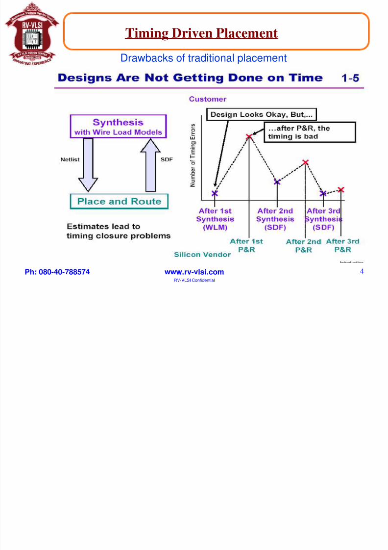
Timing Driven Placement
Drawbacks of traditional placement
8/3/2019 pd design 6
http://slidepdf.com/reader/full/pd-design-6 5/44
Ph: 080-40-788574 www.rv-vlsi.comRV-VLSI Confidential
5
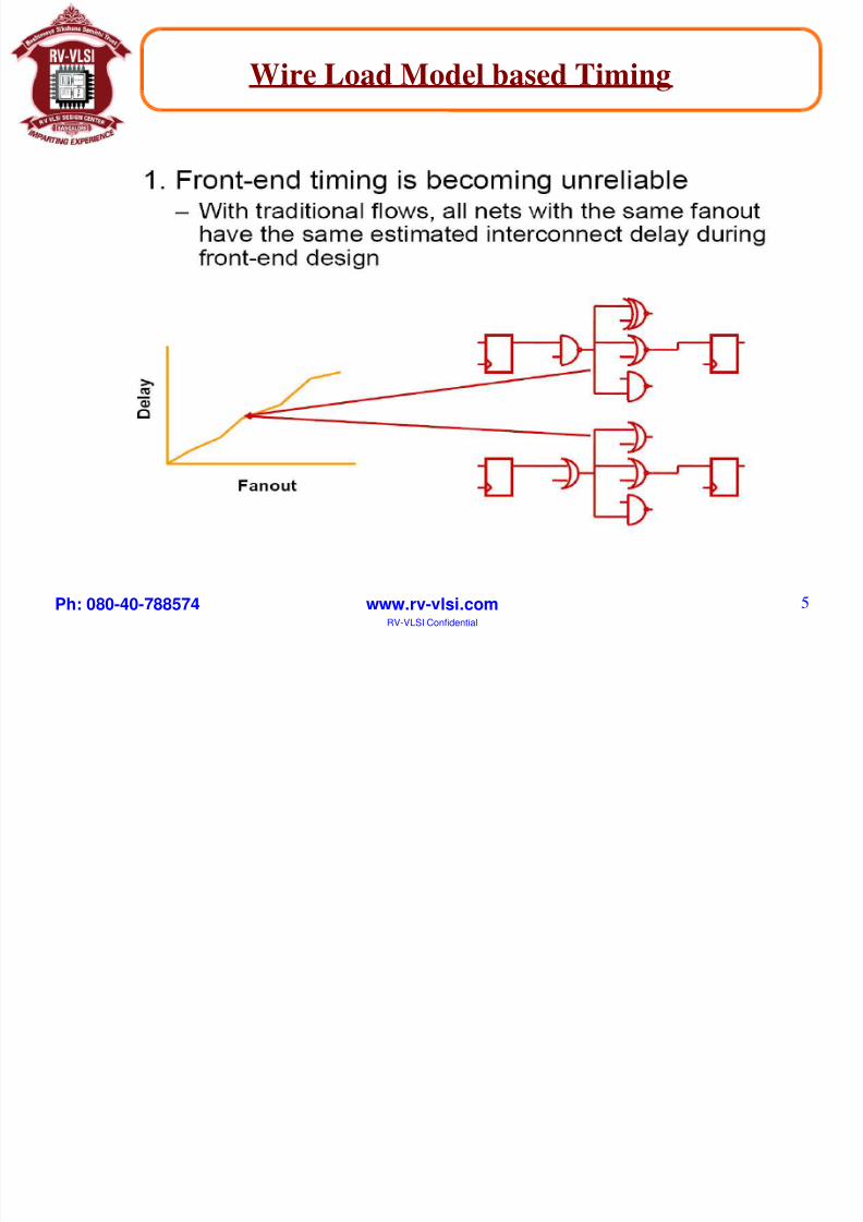
Wire Load Model based Timing
8/3/2019 pd design 6
http://slidepdf.com/reader/full/pd-design-6 6/44
Ph: 080-40-788574 www.rv-vlsi.comRV-VLSI Confidential
6
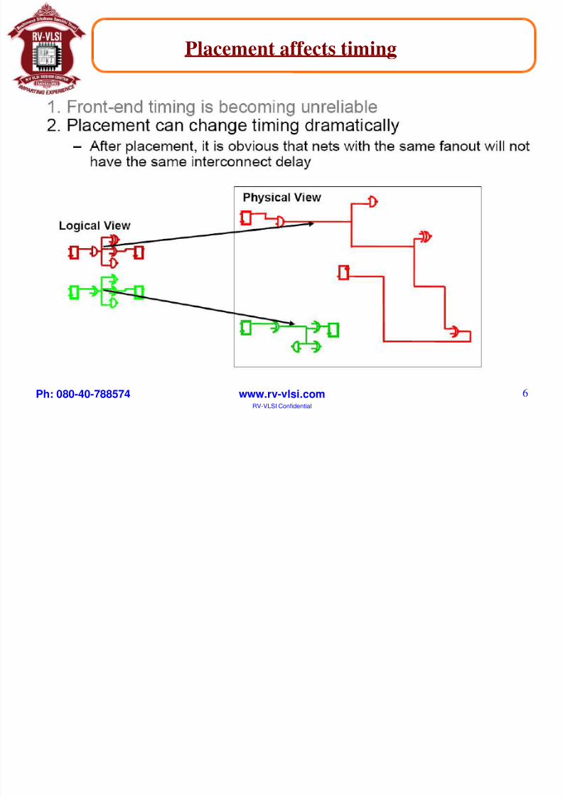
Placement affects timing
8/3/2019 pd design 6
http://slidepdf.com/reader/full/pd-design-6 7/44
Ph: 080-40-788574 www.rv-vlsi.comRV-VLSI Confidential
7
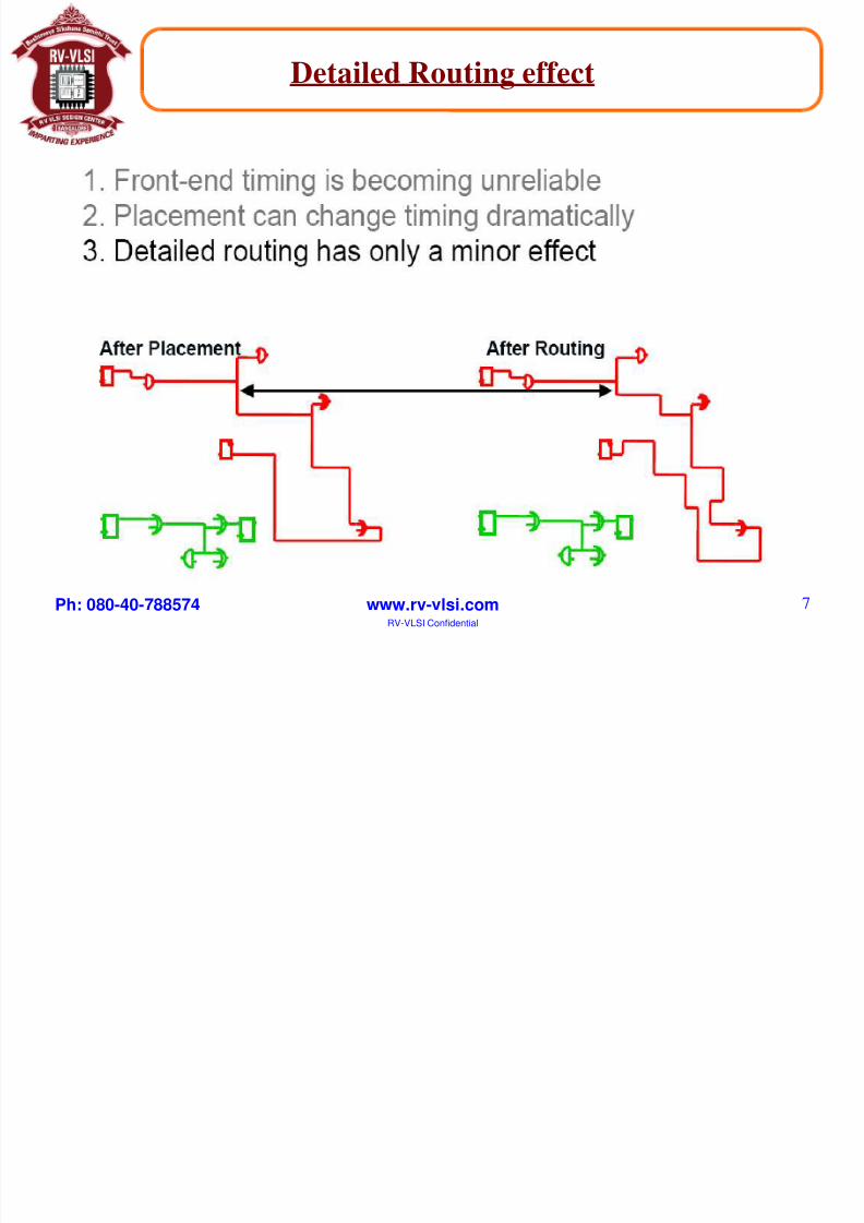
Detailed Routing effect
8/3/2019 pd design 6
http://slidepdf.com/reader/full/pd-design-6 8/44
Ph: 080-40-788574 www.rv-vlsi.comRV-VLSI Confidential
8
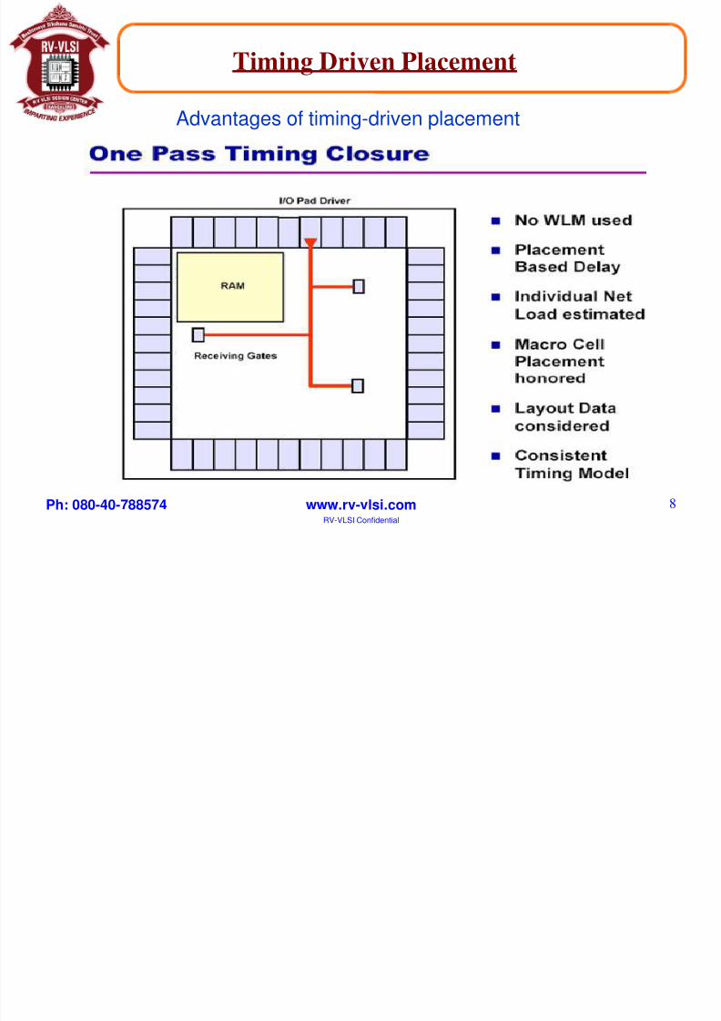
Advantages of timing-driven placement
Timing Driven Placement
8/3/2019 pd design 6
http://slidepdf.com/reader/full/pd-design-6 9/44
Ph: 080-40-788574 www.rv-vlsi.comRV-VLSI Confidential
9
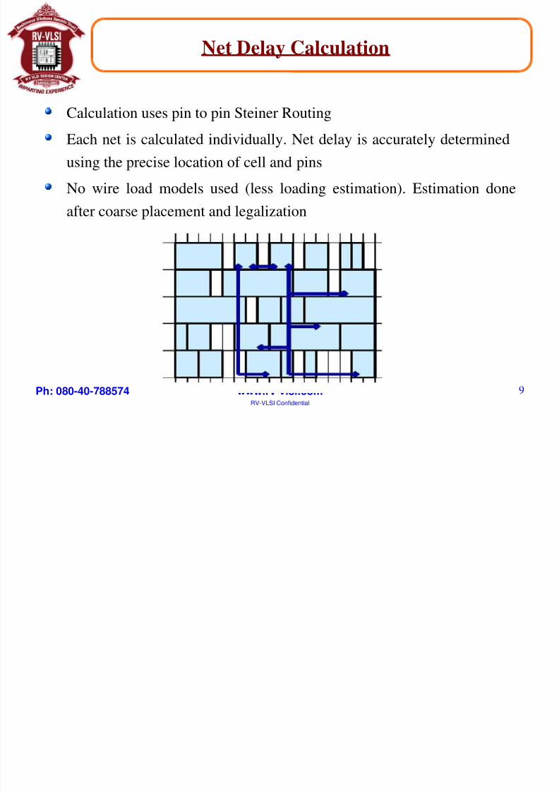
Net Delay Calculation
Calculation uses pin to pin Steiner Routing
Each net is calculated individually. Net delay is accurately determined
using the precise location of cell and pins
No wire load models used (less loading estimation). Estimation doneafter coarse placement and legalization
8/3/2019 pd design 6
http://slidepdf.com/reader/full/pd-design-6 10/44
Ph: 080-40-788574 www.rv-vlsi.comRV-VLSI Confidential
10
Placement Goals
Guarantee the router can complete the routing step
Minimize all the critical net delays
Make the chip as dense as possible
8/3/2019 pd design 6
http://slidepdf.com/reader/full/pd-design-6 11/44
Ph: 080-40-788574 www.rv-vlsi.comRV-VLSI Confidential
11
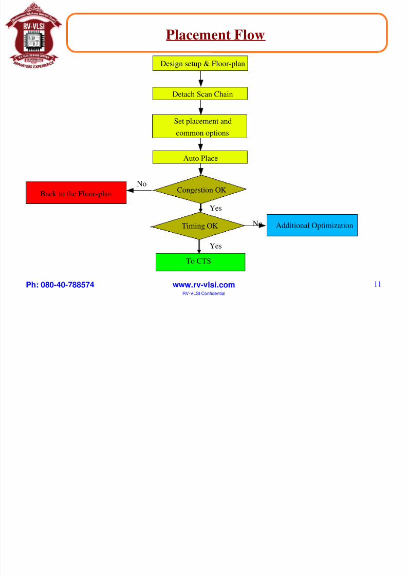
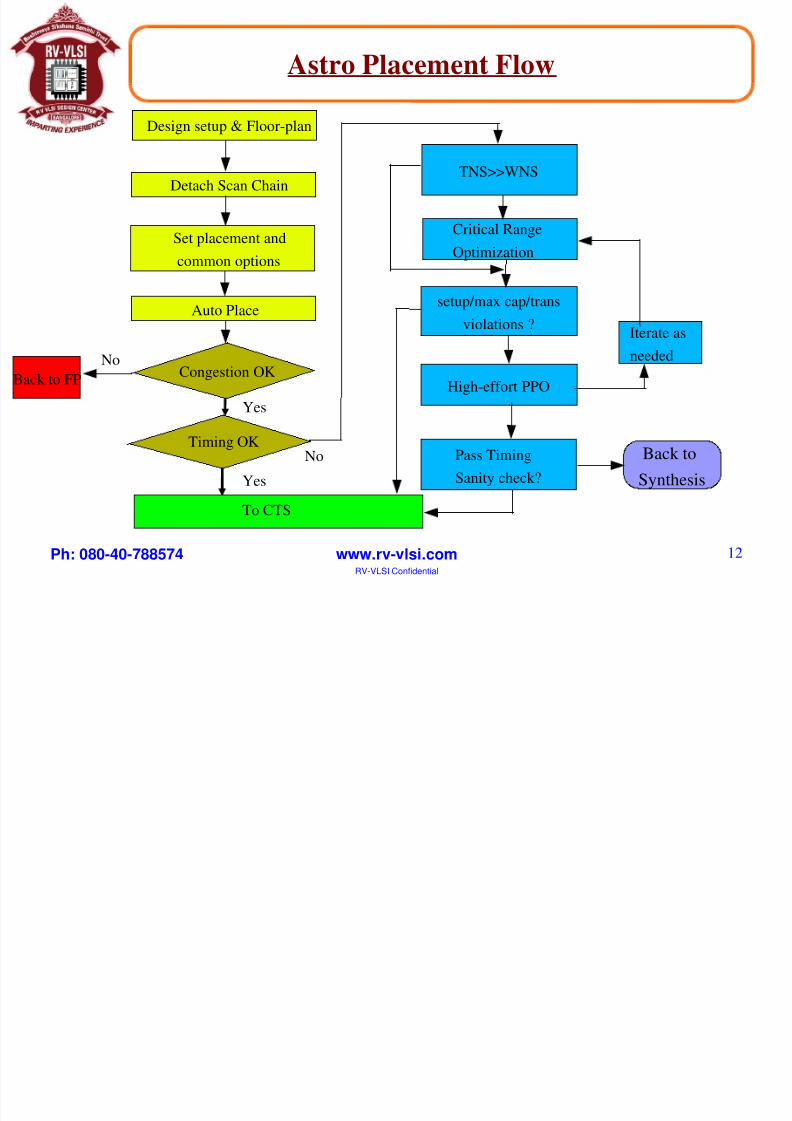
Placement Flow
Design setup & Floor-plan
Detach Scan Chain
Set placement and
common options
Auto Place
Back to the Floor-plan
To CTS
Additional Optimization
No
Yes
No
Yes
Congestion OK
Timing OK
8/3/2019 pd design 6
http://slidepdf.com/reader/full/pd-design-6 12/44
Ph: 080-40-788574 www.rv-vlsi.comRV-VLSI Confidential
12
Astro Placement Flow
Critical Range
Optimization
High-effort PPO
Iterate as
needed
Back to
Synthesis
TNS>>WNS
setup/max cap/trans
violations ?
Pass Timing
Sanity check?
Design setup & Floor-plan
Detach Scan Chain
Set placement and
common options
Auto Place
Back to FP
To CTS
No
Yes
No
Yes
Congestion OK
Timing OK
8/3/2019 pd design 6
http://slidepdf.com/reader/full/pd-design-6 13/44
Ph: 080-40-788574 www.rv-vlsi.comRV-VLSI Confidential
13
What are Scan Chains?
Scan chains are groups of FFs that are serially connected through SI/SO
pins
Scan chain paths are active only during “test mode”, not during
“functional mode”
FFs are typically connected in alphanumeric order during synthesis –
irrelevant for DFT, but not optimal for routing
8/3/2019 pd design 6
http://slidepdf.com/reader/full/pd-design-6 14/44
Ph: 080-40-788574 www.rv-vlsi.comRV-VLSI Confidential
14
Issue with scan Chains
If serially connected FFs are placed far apart this may require a lot more
routing resources than necessary
If FFs are placed close together, according to their scan chain ordering,
this may hurt timing along functional critical paths
8/3/2019 pd design 6
http://slidepdf.com/reader/full/pd-design-6 15/44
Ph: 080-40-788574 www.rv-vlsi.comRV-VLSI Confidential
15
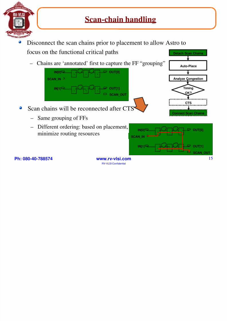
Disconnect the scan chains prior to placement to allow Astro to
focus on the functional critical paths
– Chains are ‘annotated’ first to capture the FF “grouping”
Scan chains will be reconnected after CTS
– Same grouping of FFs– Different ordering: based on placement, to
minimize routing resources
Scan-chain handling
IN[0]
SCAN_IN
OUT[0]
SCAN_OUT
IN[1] OUT[1]
IN[0]
SCAN_IN
OUT[0]
SCAN_OUT
IN[1] OUT[1]
Auto-Place
Detach Scan Chains
CTS
Connect Scan Chains
Timing
OK?
Analyze Congestion
8/3/2019 pd design 6
http://slidepdf.com/reader/full/pd-design-6 16/44
Ph: 080-40-788574 www.rv-vlsi.comRV-VLSI Confidential
16
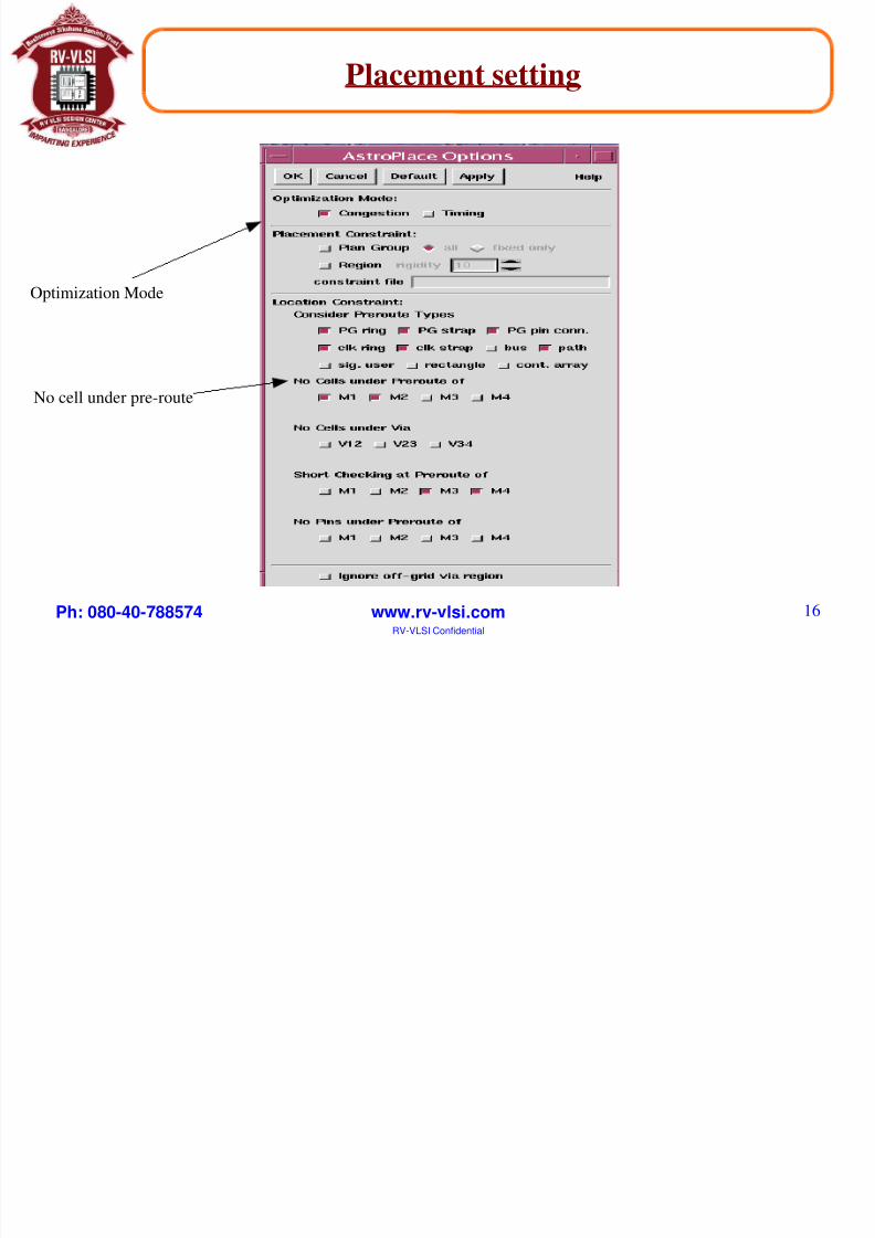
Placement setting
Optimization Mode
No cell under pre-route
8/3/2019 pd design 6
http://slidepdf.com/reader/full/pd-design-6 17/44
Ph: 080-40-788574 www.rv-vlsi.comRV-VLSI Confidential
17
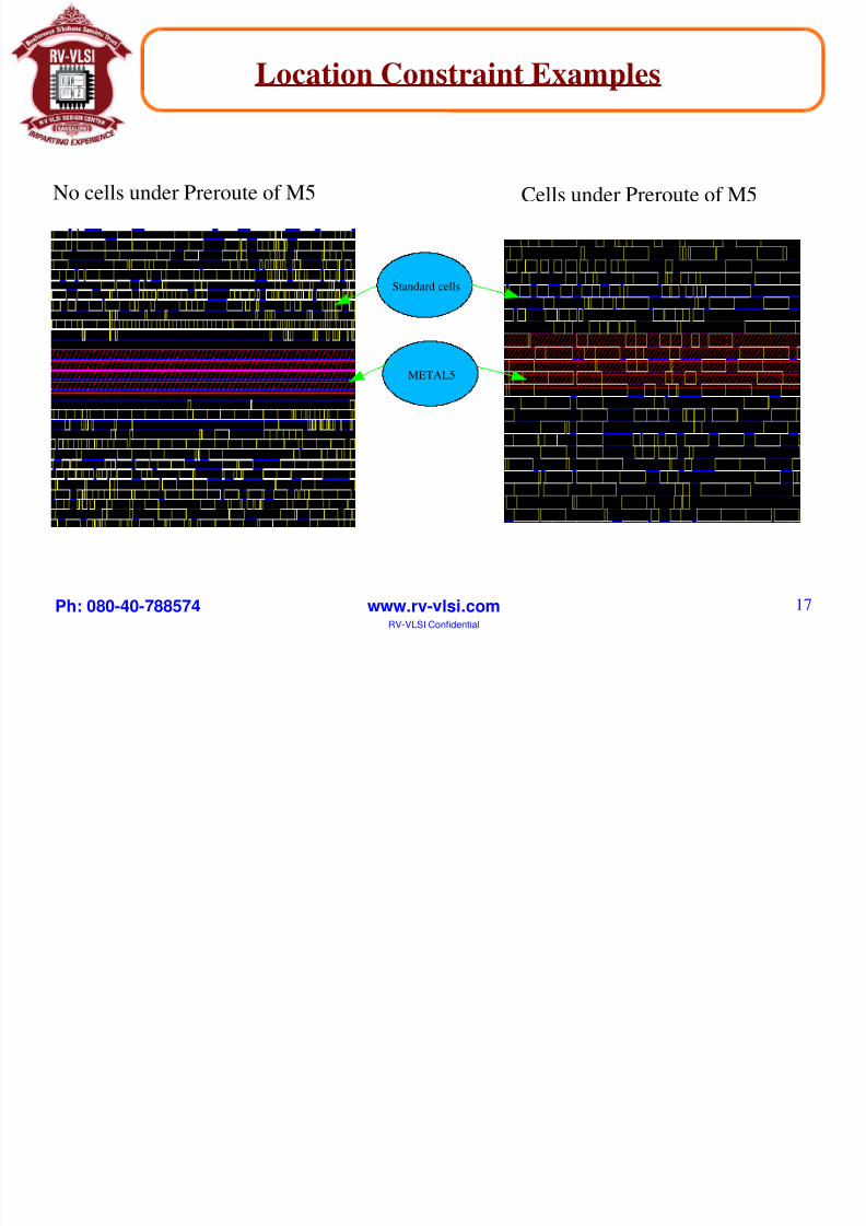
Location Constraint Examples
Standard cells
METAL5
No cells under Preroute of M5 Cells under Preroute of M5
8/3/2019 pd design 6
http://slidepdf.com/reader/full/pd-design-6 18/44
Ph: 080-40-788574 www.rv-vlsi.comRV-VLSI Confidential
18
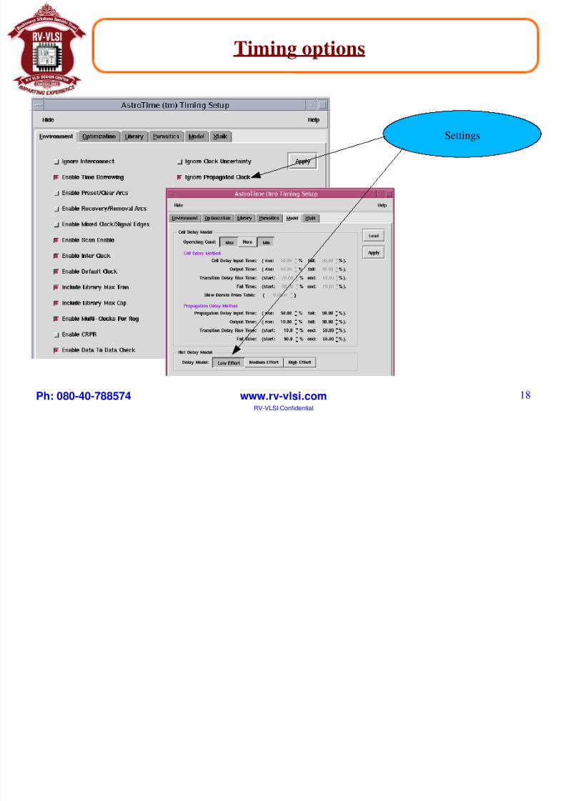
Timing options
Settings
8/3/2019 pd design 6
http://slidepdf.com/reader/full/pd-design-6 19/44
Ph: 080-40-788574 www.rv-vlsi.comRV-VLSI Confidential
19
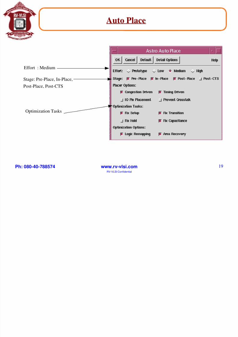
Auto Place
Effort : Medium
Stage: Pre-Place, In-Place,
Post-Place, Post-CTS
Optimization Tasks
8/3/2019 pd design 6
http://slidepdf.com/reader/full/pd-design-6 20/44
Ph: 080-40-788574 www.rv-vlsi.comRV-VLSI Confidential
20
Create Minimal “seed” Netlist for Placement
Pre-Place optimization removes all WLM effects to create a minimal “seed”
netlist uses RC = 0 to
- Perform logic synthesis to meet setup timing
- reduce total cell area by gate down sizing and buffer/inverter
removal along paths with positive setup slack.
Uses estimated RCs, based on quick “throw- away” placement, to buffer non-
clock high fanout nets.
HFN: A high fanout net is,by definition within Astro, a data (non-clock) signal
net that fans out to 10 or more cells.
8/3/2019 pd design 6
http://slidepdf.com/reader/full/pd-design-6 21/44
Ph: 080-40-788574 www.rv-vlsi.comRV-VLSI Confidential
21
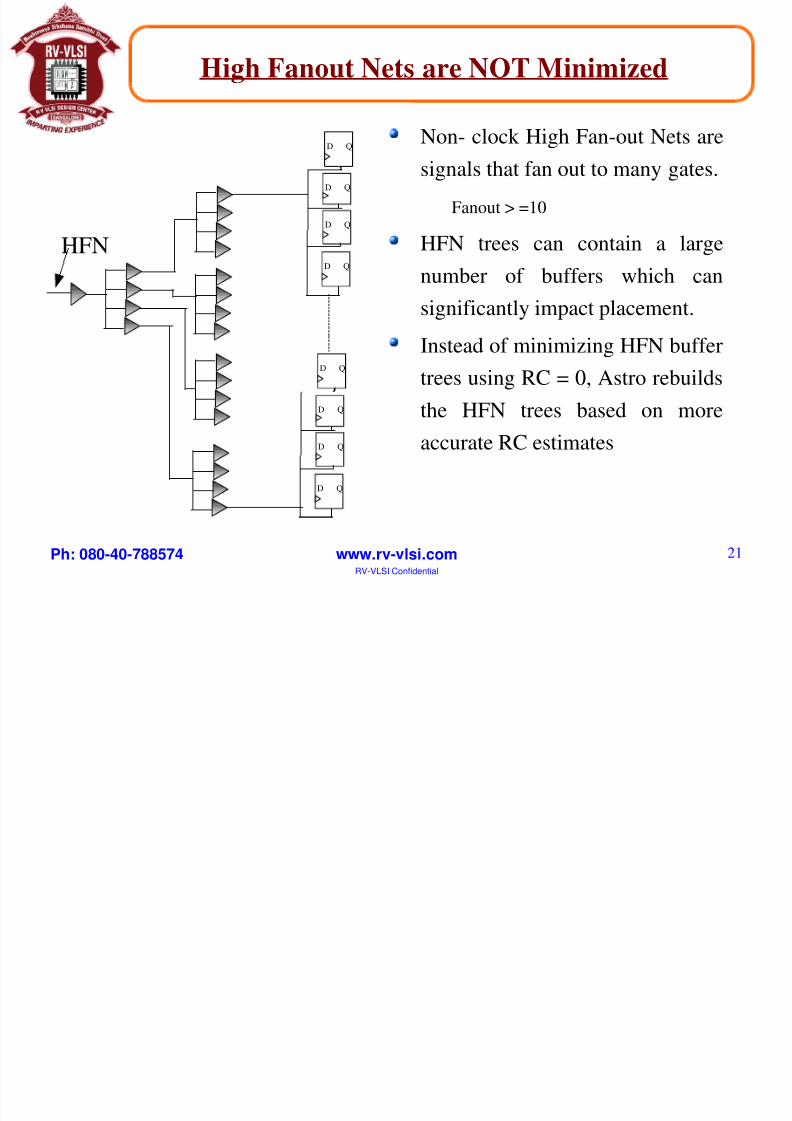
High Fanout Nets are NOT Minimized
Non- clock High Fan-out Nets aresignals that fan out to many gates.
Fanout > =10
HFN trees can contain a large
number of buffers which cansignificantly impact placement.
Instead of minimizing HFN buffer
trees using RC = 0, Astro rebuilds
the HFN trees based on moreaccurate RC estimates
D Q
D Q
D Q
D Q
D Q
D Q
D Q
D Q
HFN
8/3/2019 pd design 6
http://slidepdf.com/reader/full/pd-design-6 22/44
Ph: 080-40-788574 www.rv-vlsi.comRV-VLSI Confidential
22
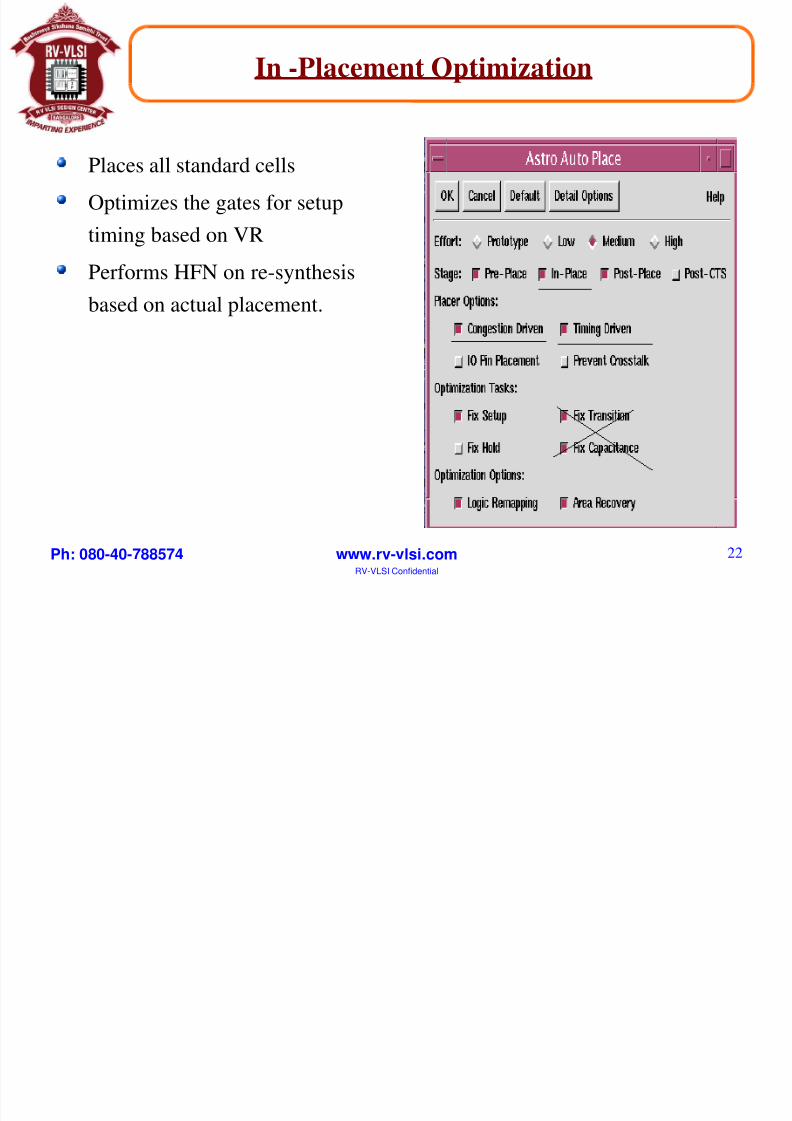
In -Placement Optimization
Places all standard cells
Optimizes the gates for setup
timing based on VR
Performs HFN on re-synthesisbased on actual placement.
8/3/2019 pd design 6
http://slidepdf.com/reader/full/pd-design-6 23/44
Ph: 080-40-788574 www.rv-vlsi.comRV-VLSI Confidential
23
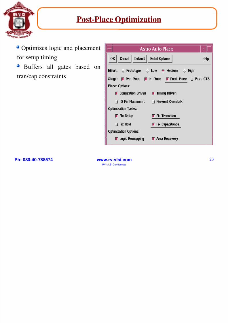
Post-Place Optimization
Optimizes logic and placement
for setup timing
Buffers all gates based on
tran/cap constraints
8/3/2019 pd design 6
http://slidepdf.com/reader/full/pd-design-6 24/44
Ph: 080-40-788574 www.rv-vlsi.comRV-VLSI Confidential
24
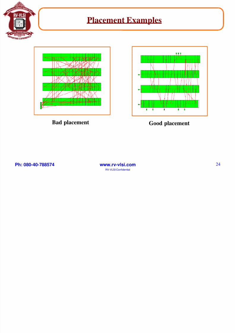
Bad placement Good placement
Placement Examples
8/3/2019 pd design 6
http://slidepdf.com/reader/full/pd-design-6 25/44
Ph: 080-40-788574 www.rv-vlsi.comRV-VLSI Confidential
25
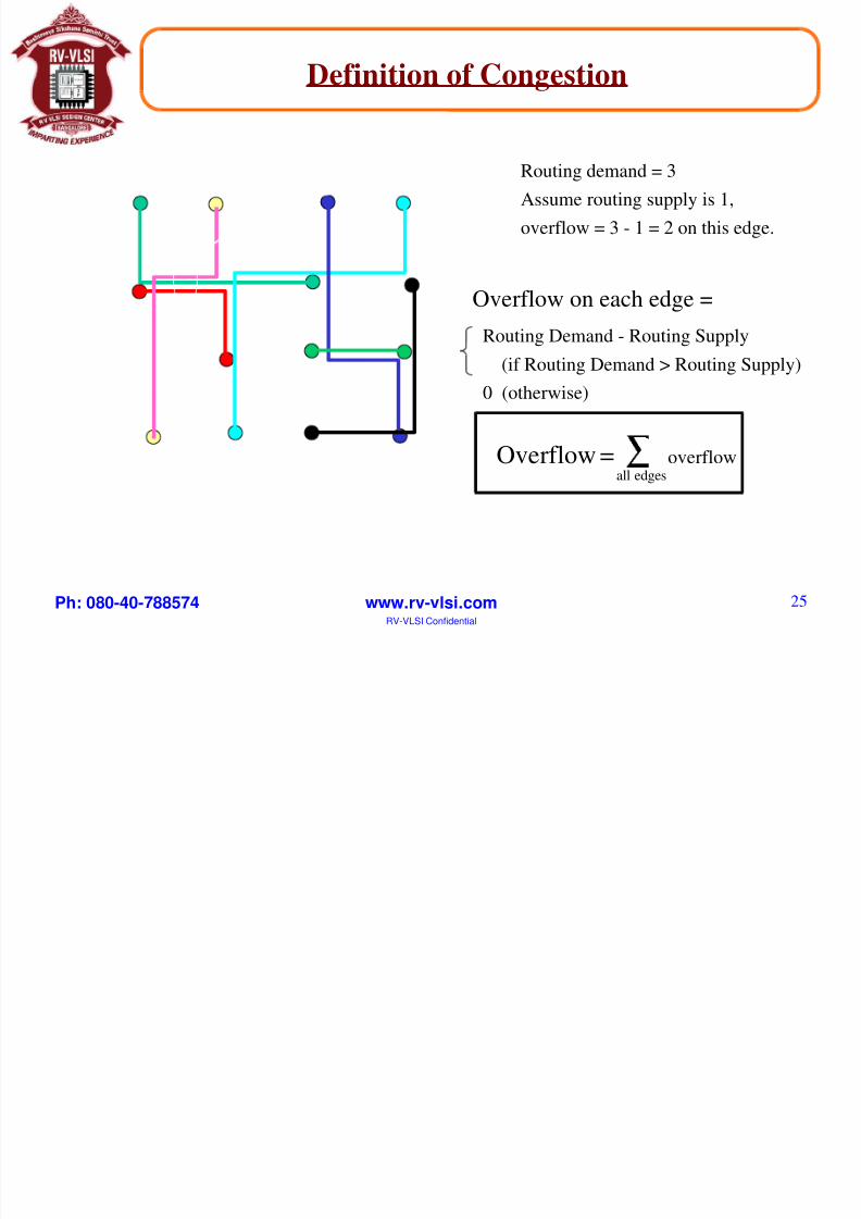
Definition of Congestion
Routing demand = 3
Assume routing supply is 1,
overflow = 3 - 1 = 2 on this edge.
Overflow = overflowall edges
Overflow on each edge =Routing Demand - Routing Supply
(if Routing Demand > Routing Supply)
0 (otherwise)
8/3/2019 pd design 6
http://slidepdf.com/reader/full/pd-design-6 26/44
Ph: 080-40-788574 www.rv-vlsi.comRV-VLSI Confidential
26
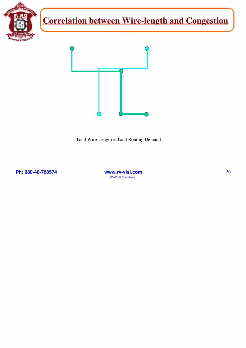
Correlation between Wire-length and Congestion
Total Wire-Length = Total Routing Demand
8/3/2019 pd design 6
http://slidepdf.com/reader/full/pd-design-6 27/44
Ph: 080-40-788574 www.rv-vlsi.comRV-VLSI Confidential
27
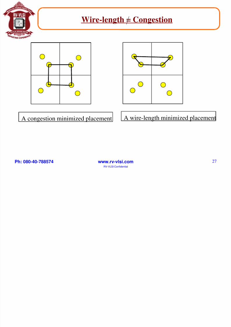
Wire-length = Congestion
A congestion minimized placement A wire-length minimized placement
8/3/2019 pd design 6
http://slidepdf.com/reader/full/pd-design-6 28/44
Ph: 080-40-788574 www.rv-vlsi.comRV-VLSI Confidential
28
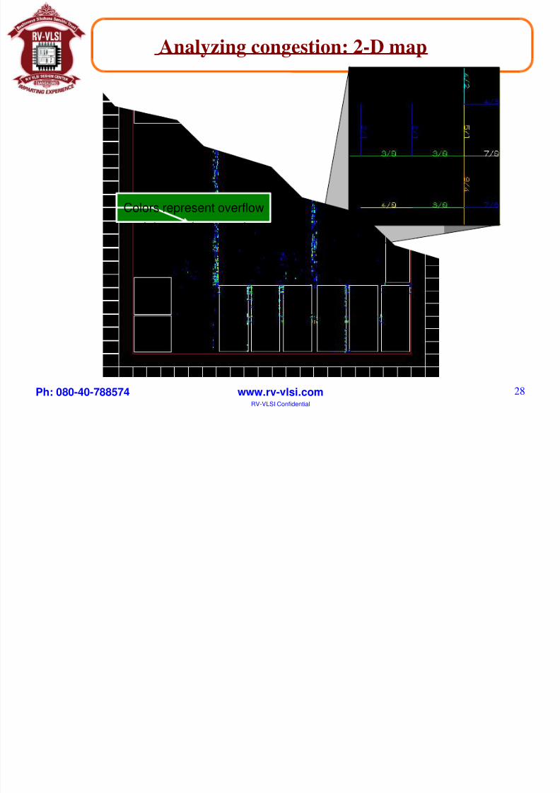
Analyzing congestion: 2-D map
Colors represent overflow
of demand vs. supply
8/3/2019 pd design 6
http://slidepdf.com/reader/full/pd-design-6 29/44
Ph: 080-40-788574 www.rv-vlsi.comRV-VLSI Confidential
29
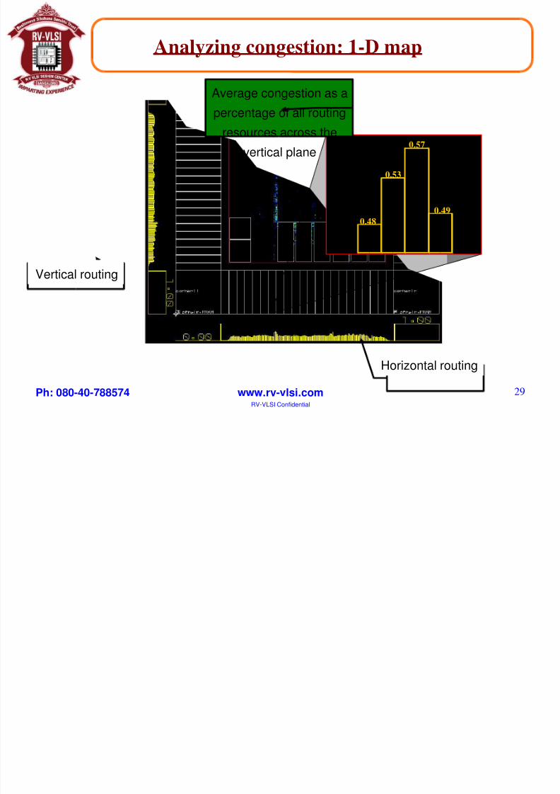
Analyzing congestion: 1-D map
Vertical routing
Horizontal routing
0.48
0.57
0.49
0.53
Average congestion as a
percentage of all routing
resources across the
vertical plane
8/3/2019 pd design 6
http://slidepdf.com/reader/full/pd-design-6 30/44
Ph: 080-40-788574 www.rv-vlsi.comRV-VLSI Confidential
30
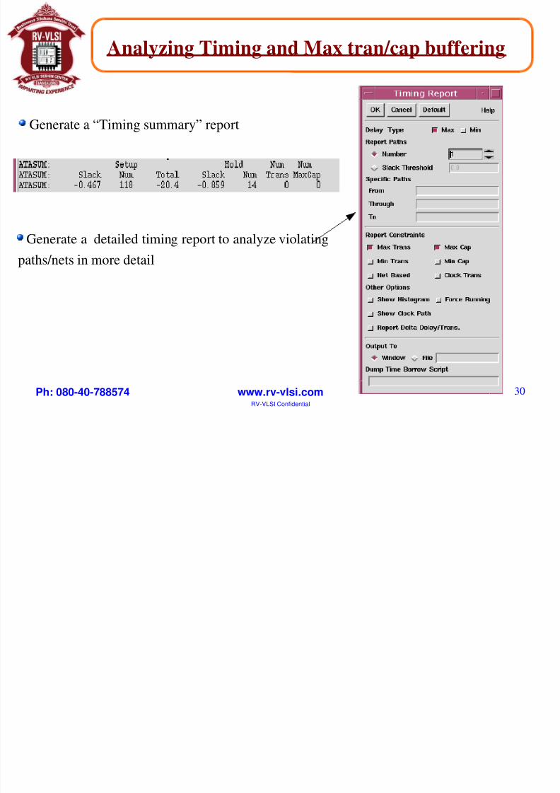
Analyzing Timing and Max tran/cap buffering
Generate a “Timing summary” report
Generate a detailed timing report to analyze violating
paths/nets in more detail
8/3/2019 pd design 6
http://slidepdf.com/reader/full/pd-design-6 31/44
Ph: 080-40-788574 www.rv-vlsi.comRV-VLSI Confidential
31
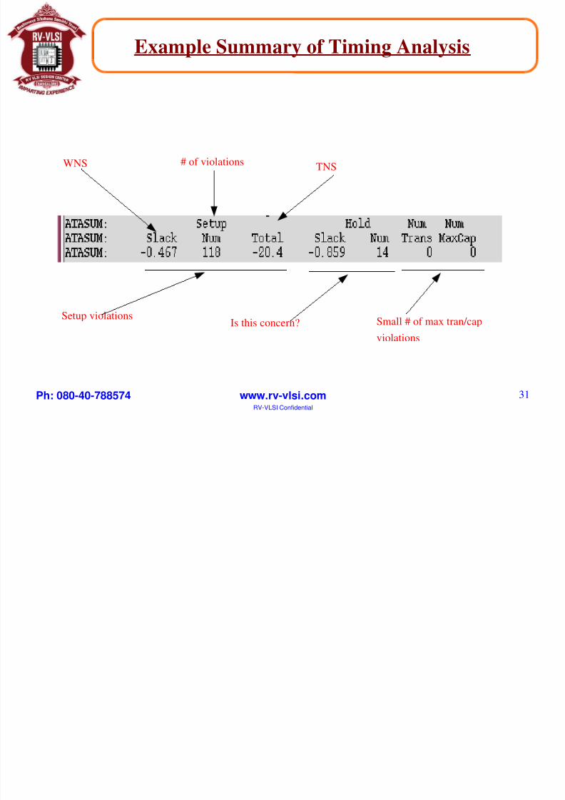
Example Summary of Timing Analysis
WNS # of violationsTNS
Setup violationsIs this concern? Small # of max tran/cap
violations
8/3/2019 pd design 6
http://slidepdf.com/reader/full/pd-design-6 32/44
Ph: 080-40-788574 www.rv-vlsi.comRV-VLSI Confidential
32
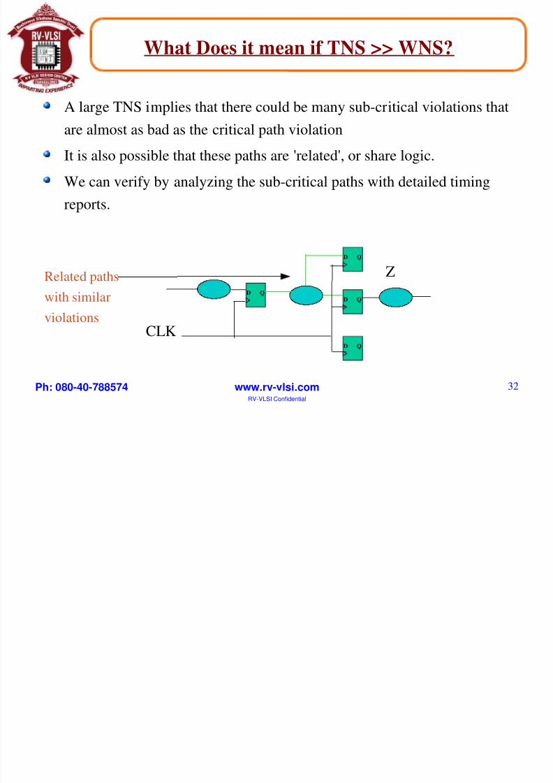
What Does it mean if TNS >> WNS?
A large TNS implies that there could be many sub-critical violations that
are almost as bad as the critical path violation
It is also possible that these paths are 'related', or share logic.
We can verify by analyzing the sub-critical paths with detailed timing
reports.
D Q
D Q
D Q
D Q
CLK
ZRelated paths
with similar
violations
8/3/2019 pd design 6
http://slidepdf.com/reader/full/pd-design-6 33/44
Ph: 080-40-788574 www.rv-vlsi.comRV-VLSI Confidential
33
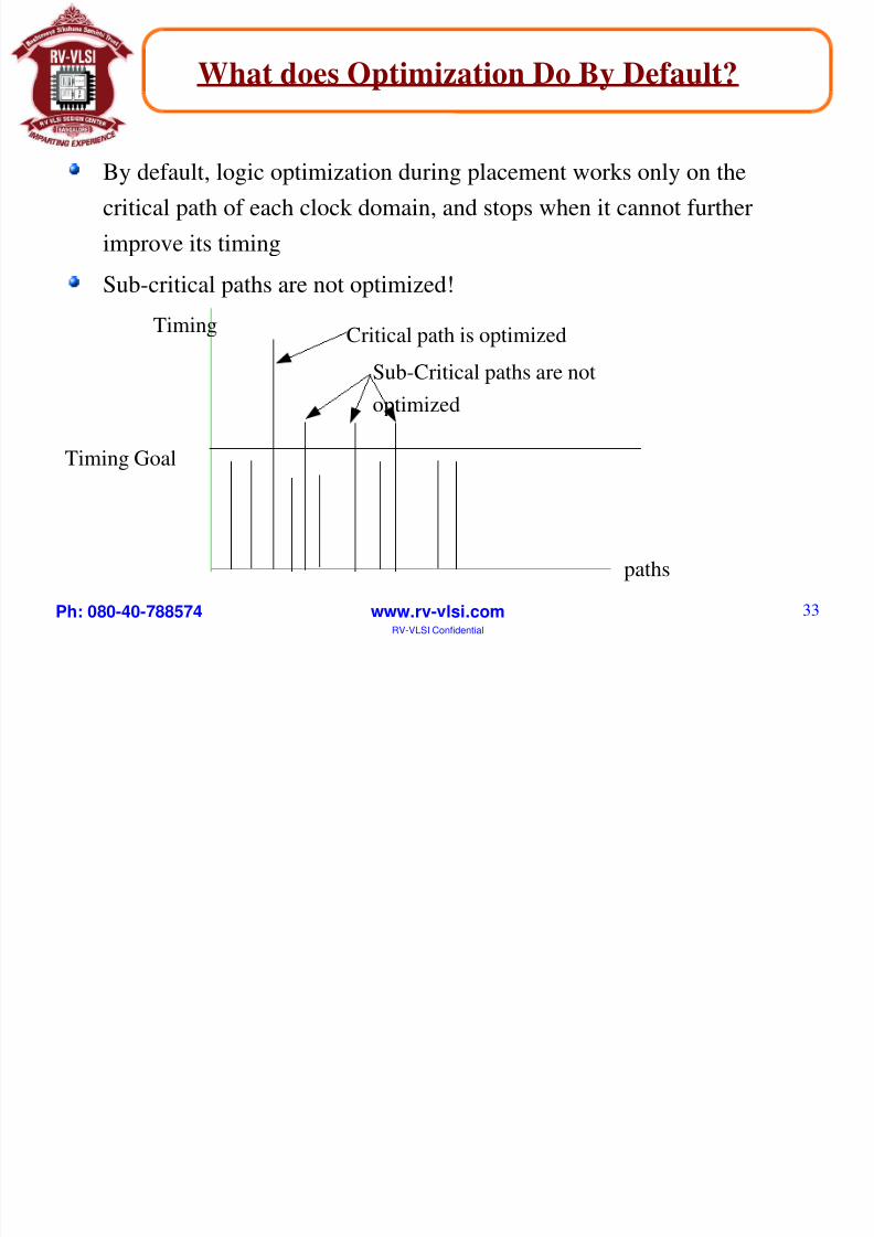
What does Optimization Do By Default?
By default, logic optimization during placement works only on the
critical path of each clock domain, and stops when it cannot further
improve its timing
Sub-critical paths are not optimized!
Critical path is optimized
Sub-Critical paths are not
optimized
paths
Timing
Timing Goal
8/3/2019 pd design 6
http://slidepdf.com/reader/full/pd-design-6 34/44
Ph: 080-40-788574 www.rv-vlsi.comRV-VLSI Confidential
34
If TNS >> WNS Critical Range Optimization
Critical Range Optimization (CRO) works on the sub critical paths,
which reduces the total number of violations paths and the TNS
CRO may also help to reduce the critical path violations if it is 'related'
to some of the sub-critical paths
8/3/2019 pd design 6
http://slidepdf.com/reader/full/pd-design-6 35/44
Ph: 080-40-788574 www.rv-vlsi.comRV-VLSI Confidential
35
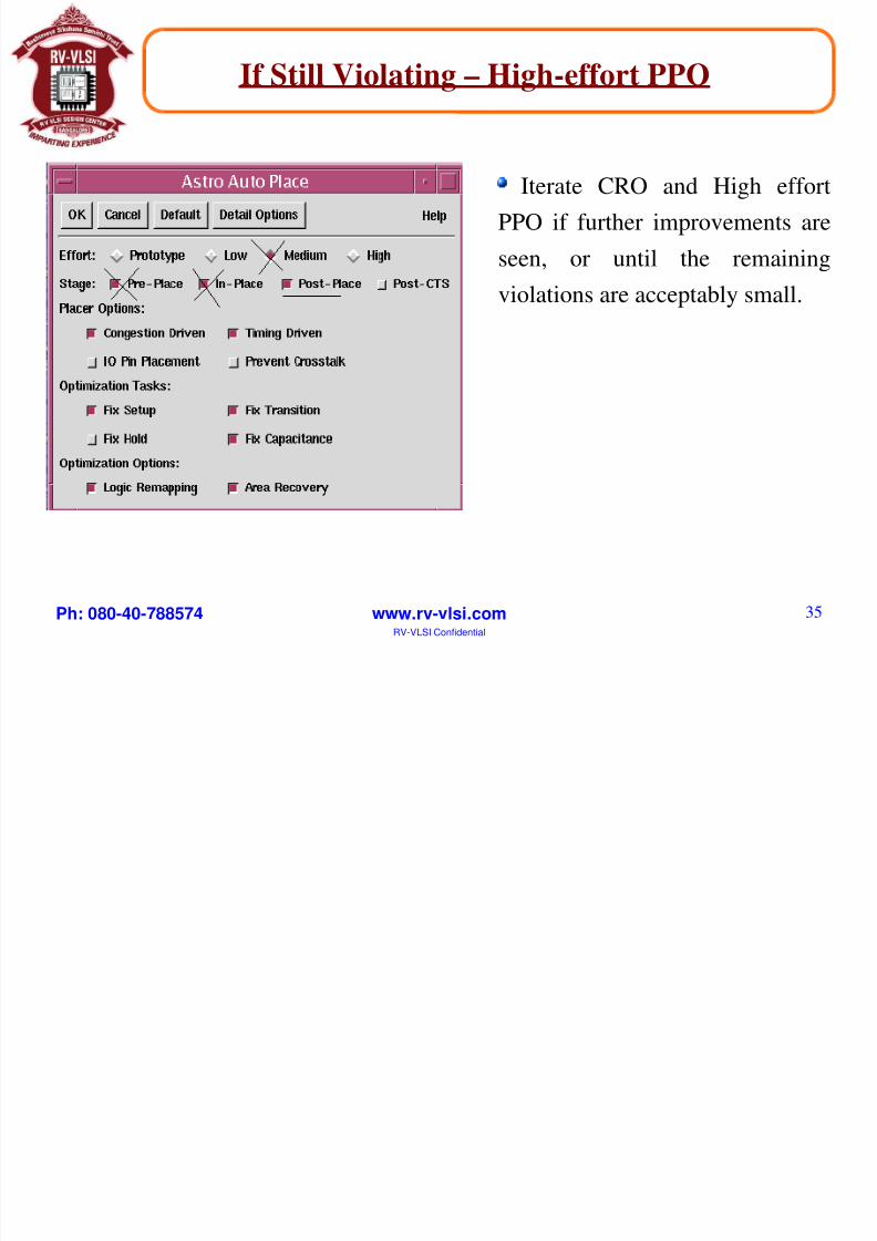
If Still Violating – High-effort PPO
Iterate CRO and High effort
PPO if further improvements are
seen, or until the remaining
violations are acceptably small.
8/3/2019 pd design 6
http://slidepdf.com/reader/full/pd-design-6 36/44
Ph: 080-40-788574 www.rv-vlsi.comRV-VLSI Confidential
36
Zero Interconnect Timing Analysis
After PPO+CRO you may still be left with a few timing violations
Perform a 'Timing Sanity Check', or zero-interconnect timing analysis.
Check the violations
– If zero violations : Continue on to CTS
– If still violating : Go back to Synthesis!
8/3/2019 pd design 6
http://slidepdf.com/reader/full/pd-design-6 37/44
Ph: 080-40-788574 www.rv-vlsi.comRV-VLSI Confidential
37
Module Takeaway
After completion of this program students will be familiar with the
Placement flow, Placement optimization, and will be ready to do the
placement for any design
8/3/2019 pd design 6
http://slidepdf.com/reader/full/pd-design-6 38/44
Ph: 080-40-788574 www.rv-vlsi.comRV-VLSI Confidential
38
Backup
8/3/2019 pd design 6
http://slidepdf.com/reader/full/pd-design-6 39/44
Ph: 080-40-788574 www.rv-vlsi.comRV-VLSI Confidential39
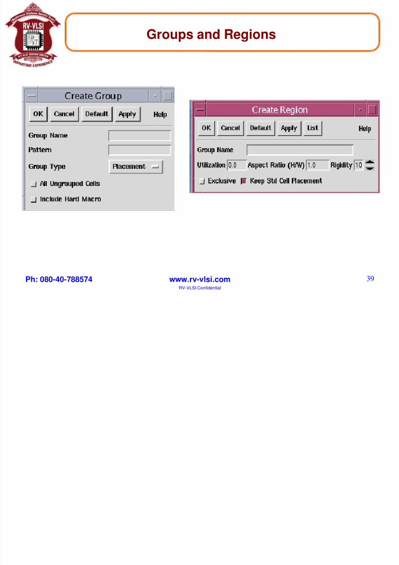
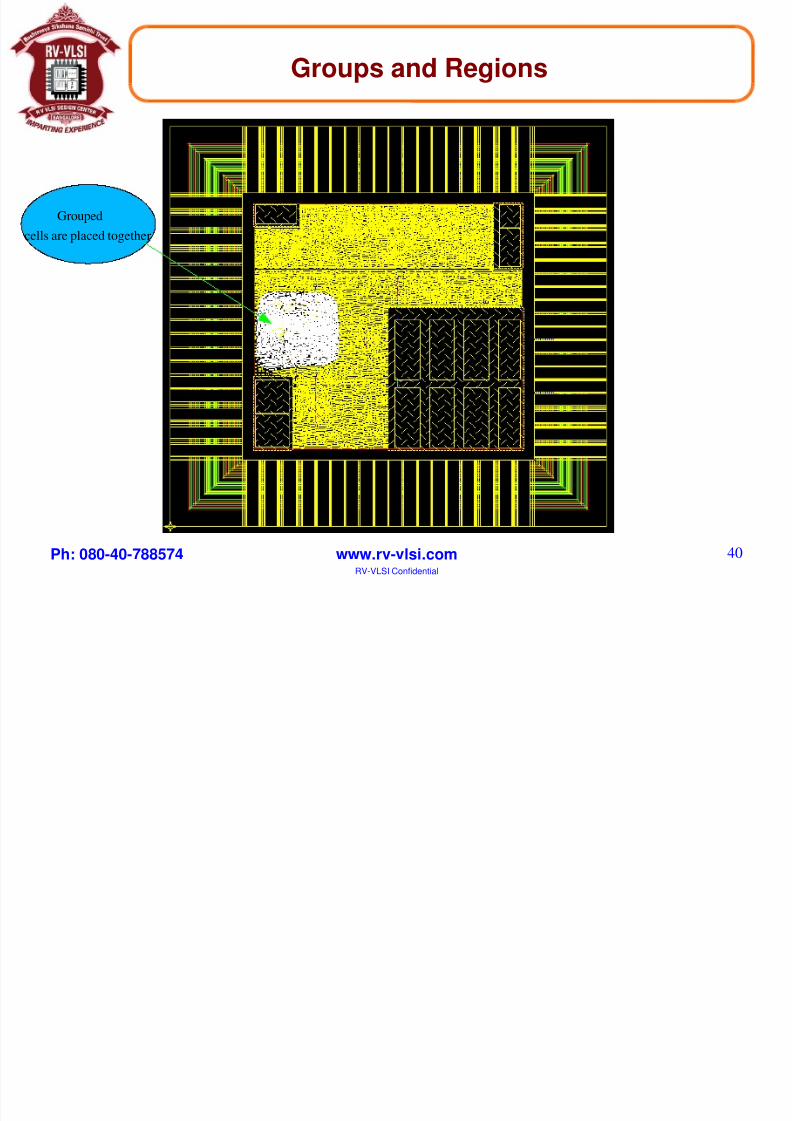
Groups and Regions
8/3/2019 pd design 6
http://slidepdf.com/reader/full/pd-design-6 40/44
Ph: 080-40-788574 www.rv-vlsi.comRV-VLSI Confidential40
Groups and Regions
Grouped
cells are placed together
8/3/2019 pd design 6
http://slidepdf.com/reader/full/pd-design-6 41/44
Ph: 080-40-788574 www.rv-vlsi.comRV-VLSI Confidential41
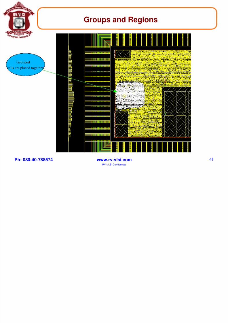
Groups and Regions
Grouped
cells are placed together
8/3/2019 pd design 6
http://slidepdf.com/reader/full/pd-design-6 42/44
Ph: 080-40-788574 www.rv-vlsi.comRV-VLSI Confidential42
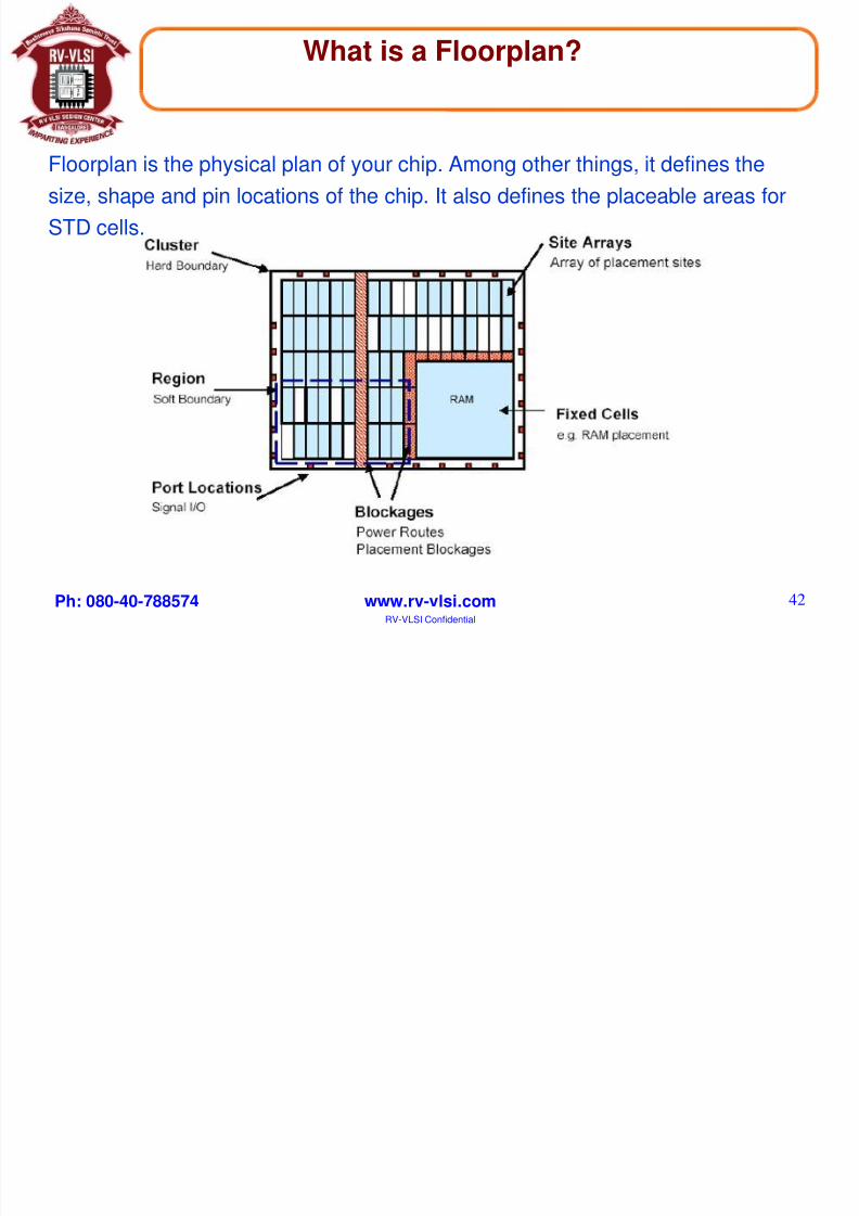
What is a Floorplan?
Floorplan is the physical plan of your chip. Among other things, it defines the
size, shape and pin locations of the chip. It also defines the placeable areas for
STD cells.
8/3/2019 pd design 6
http://slidepdf.com/reader/full/pd-design-6 43/44
Ph: 080-40-788574 www.rv-vlsi.comRV-VLSI Confidential43
What is “placement” ?
● “Placement” is a way of assigning physical locations for the cells
described in the logical gate-level netlist.
● “Placeable” cells will be placed onto “sites” (sitting on site arrays)
which are defined in the floorplan.
8/3/2019 pd design 6
http://slidepdf.com/reader/full/pd-design-6 44/44
Topics
● The basics
– What are floorplan and placement ?
– Why Timing-driven-placement (TDP)
● Advantages of TDP vs. traditional placement.