Embed Size (px)
DESCRIPTION
Scanning electron microscopy
Citation preview
Effect of accelerating voltage1a
SEM image are taken at , Working distance = 12 mm at 100KX magnification and 2,5, 10 and 20 KV, (A-D) of potential
In general, increasing the accelerating voltage will decrease the spherical aberration of the system and therefore increase the resolution. Since the working distance is 12 mm it is better to have a higher voltage to get better resolution of the image. The image shown above shows the similar trend.
BA
C D
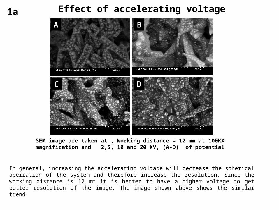
1b Effect of accelerating voltage
SEM image are taken at , Working distance = 12 mm at 25 KX magnification and 2,5, 10 and 20 KV (A-D) of potential
Since the working distance is 12 mm it is better to have a higher voltage to get better resolution of the image. The image shown above shows the similar trend.
BA
C D
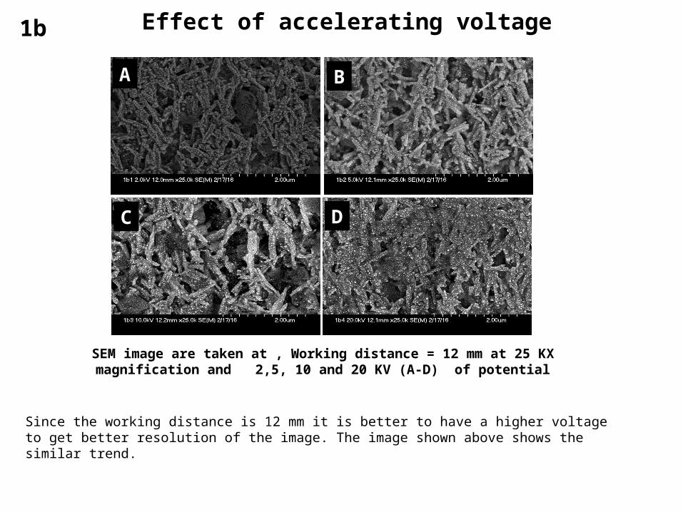
1c Effect of accelerating voltage
SEM image are taken at , Working distance = 6 mm at 100KX magnification and 2,5, 10 and 20 KV (A-D) of potential
In general, increasing the accelerating voltage will decrease the spherical aberration of the system and therefore increase the resolution. In this case the working distance is 6 mm, So there can be an effect on the beam-specimen interaction. If a higher accelerating voltage is used, the interaction volume between the beam and the specimen will become bigger because of the greater energy of the beam of electrons therefore then accelerating voltage does not has much effect on the resolution of the images. In the above Image 1c (10 KV of accelerating voltage) has higher resolution.
BA
C D
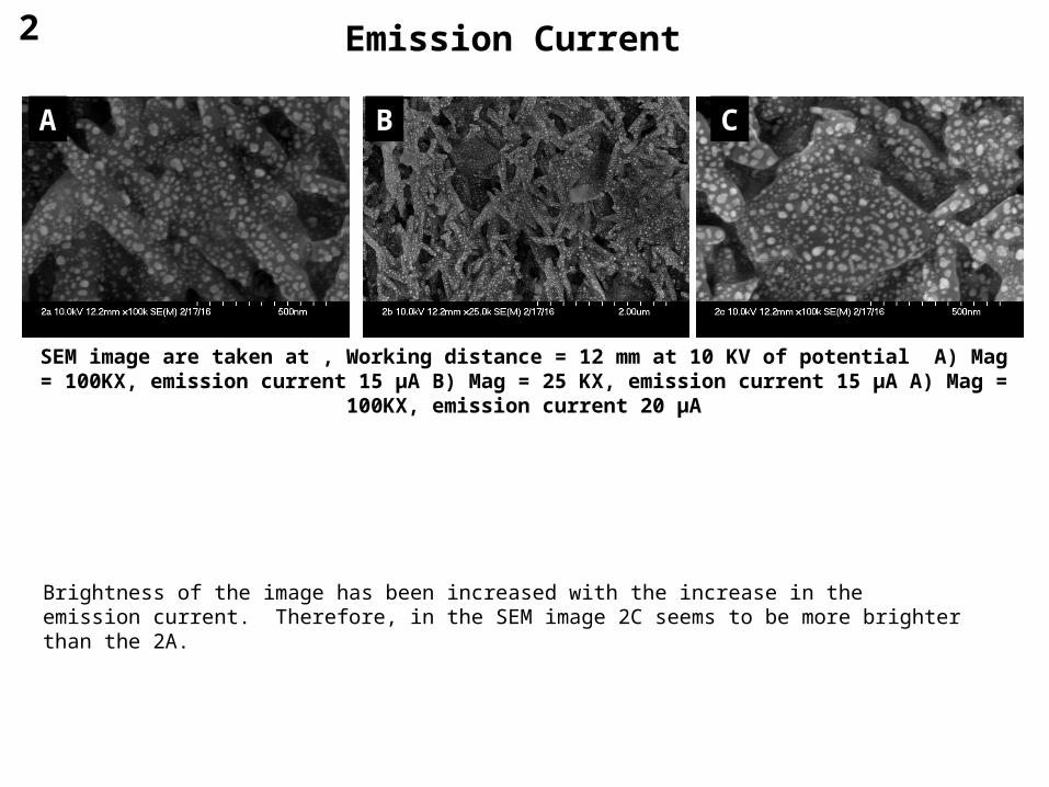
2 Emission Current
BA C
SEM image are taken at , Working distance = 12 mm at 10 KV of potential A) Mag = 100KX, emission current 15 µA B) Mag = 25 KX, emission current 15 µA A) Mag = 100KX, emission current 20 µA
Brightness of the image has been increased with the increase in the emission current. Therefore, in the SEM image 2C seems to be more brighter than the 2A.
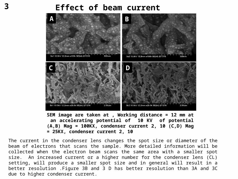
3 Effect of beam current
SEM image are taken at , Working distance = 12 mm at an accelerating potential of 10 KV of potential (A,B) Mag = 100KX, condenser current 2, 10 (C,D) Mag = 25KX, condenser current 2, 10
The current in the condenser lens changes the spot size or diameter of the beam of electrons that scans the sample. More detailed information will be collected when the electron beam scans the same area with a smaller spot size. An increased current or a higher number for the condenser lens (CL) setting, will produce a smaller spot size and in general will result in a better resolution .Figure 3B and 3 D has better resolution than 3A and 3C due to higher condenser current.
BA
C D
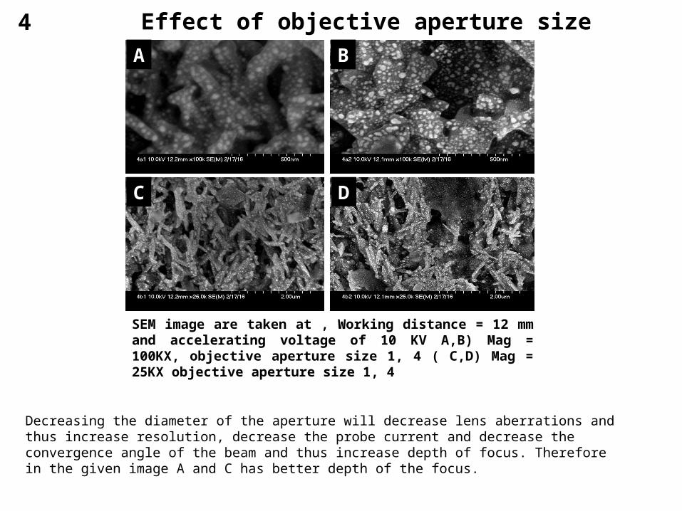
4 Effect of objective aperture size
SEM image are taken at , Working distance = 12 mm and accelerating voltage of 10 KV A,B) Mag = 100KX, objective aperture size 1, 4 ( C,D) Mag = 25KX objective aperture size 1, 4
Decreasing the diameter of the aperture will decrease lens aberrations and thus increase resolution, decrease the probe current and decrease the convergence angle of the beam and thus increase depth of focus. Therefore in the given image A and C has better depth of the focus.
BA
C D
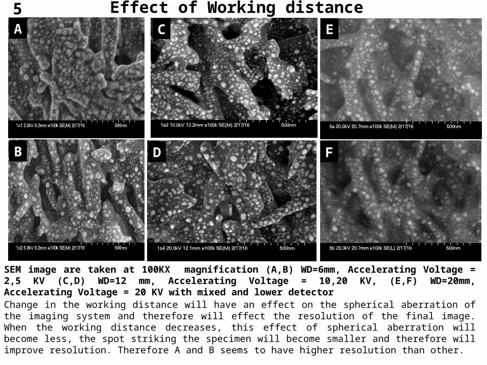
Effect of Working distance5
SEM image are taken at 100KX magnification (A,B) WD=6mm, Accelerating Voltage = 2,5 KV (C,D) WD=12 mm, Accelerating Voltage = 10,20 KV, (E,F) WD=20mm, Accelerating Voltage = 20 KV with mixed and lower detectorChange in the working distance will have an effect on the spherical aberration of the imaging system and therefore will effect the resolution of the final image. When the working distance decreases, this effect of spherical aberration will become less, the spot striking the specimen will become smaller and therefore will improve resolution. Therefore A and B seems to have higher resolution than other.
B
A C
F
E
D
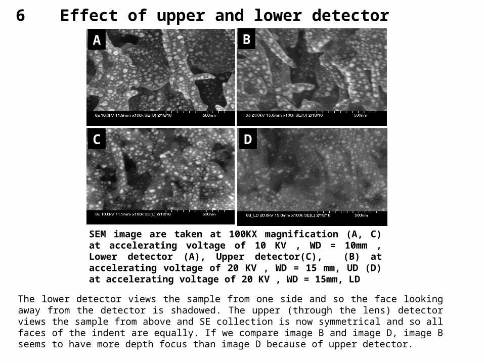
6 Effect of upper and lower detector
SEM image are taken at 100KX magnification (A, C) at accelerating voltage of 10 KV , WD = 10mm , Lower detector (A), Upper detector(C), (B) at accelerating voltage of 20 KV , WD = 15 mm, UD (D) at accelerating voltage of 20 KV , WD = 15mm, LD
The lower detector views the sample from one side and so the face looking away from the detector is shadowed. The upper (through the lens) detector views the sample from above and SE collection is now symmetrical and so all faces of the indent are equally. If we compare image B and image D, image B seems to have more depth focus than image D because of upper detector.
BA
C D
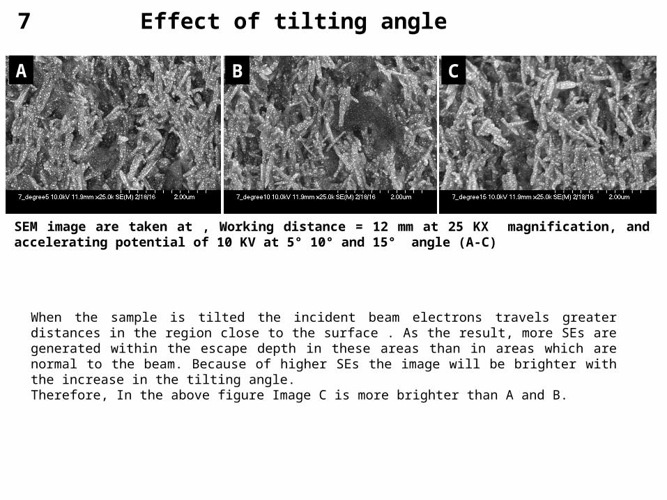
7 Effect of tilting angle
SEM image are taken at , Working distance = 12 mm at 25 KX magnification, and accelerating potential of 10 KV at 5° 10° and 15° angle (A-C)
When the sample is tilted the incident beam electrons travels greater distances in the region close to the surface . As the result, more SEs are generated within the escape depth in these areas than in areas which are normal to the beam. Because of higher SEs the image will be brighter with the increase in the tilting angle. Therefore, In the above figure Image C is more brighter than A and B.
BA C
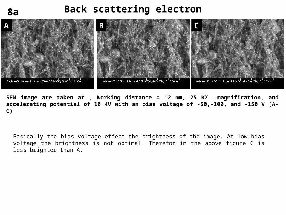
8aBA C
SEM image are taken at , Working distance = 12 mm, 25 KX magnification, and accelerating potential of 10 KV with an bias voltage of -50,-100, and -150 V (A-C)
Back scattering electron
Basically the bias voltage effect the brightness of the image. At low bias voltage the brightness is not optimal. Therefor in the above figure C is less brighter than A.
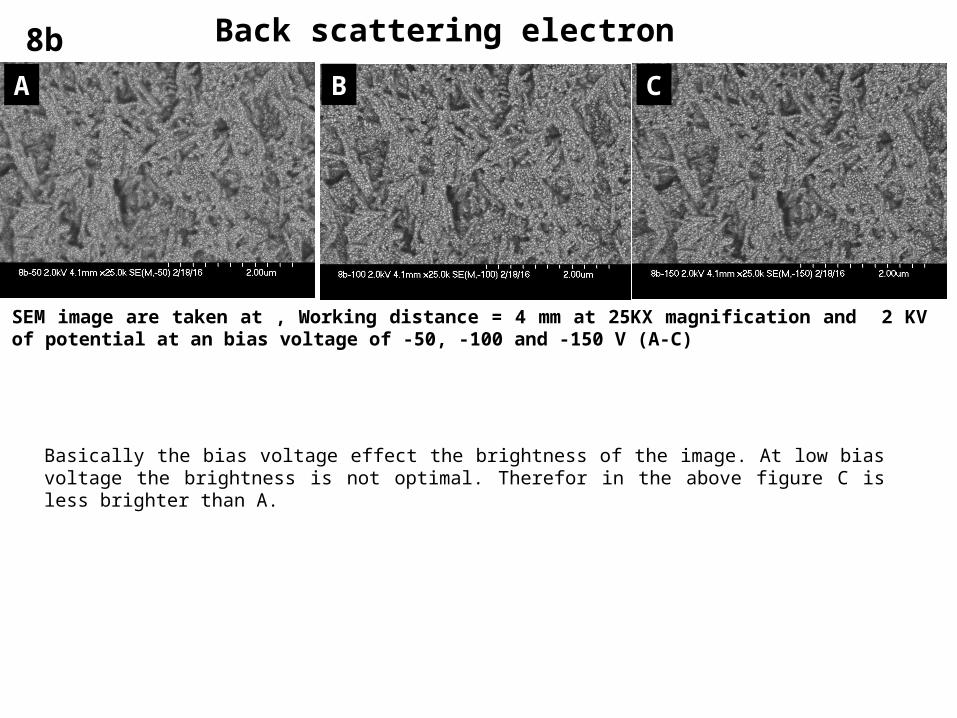
8b
SEM image are taken at , Working distance = 4 mm at 25KX magnification and 2 KV of potential at an bias voltage of -50, -100 and -150 V (A-C)
BA C
Back scattering electron
Basically the bias voltage effect the brightness of the image. At low bias voltage the brightness is not optimal. Therefor in the above figure C is less brighter than A.
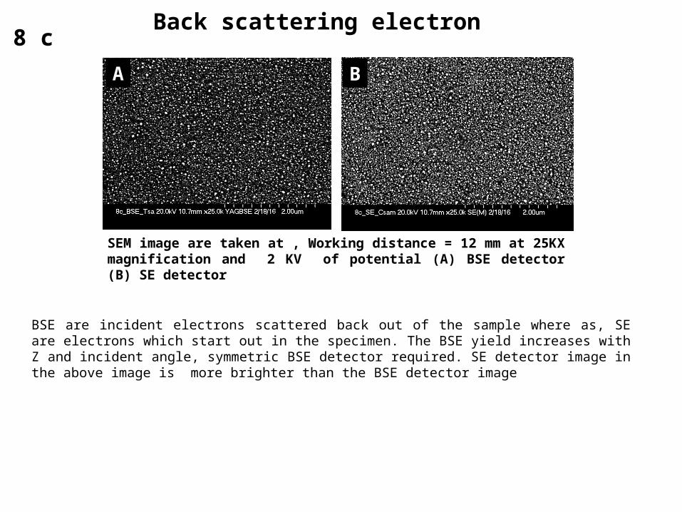
8 c Back scattering electron
BA
SEM image are taken at , Working distance = 12 mm at 25KX magnification and 2 KV of potential (A) BSE detector (B) SE detector
BSE are incident electrons scattered back out of the sample where as, SE are electrons which start out in the specimen. The BSE yield increases with Z and incident angle, symmetric BSE detector required. SE detector image in the above image is more brighter than the BSE detector image
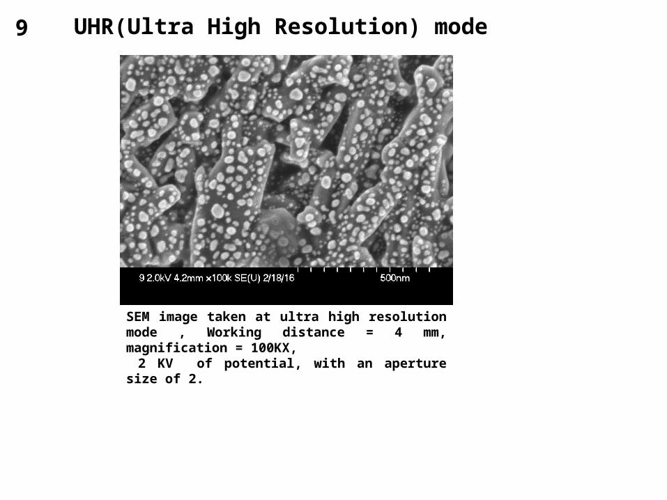
UHR(Ultra High Resolution) mode9
SEM image taken at ultra high resolution mode , Working distance = 4 mm, magnification = 100KX, 2 KV of potential, with an aperture size of 2.
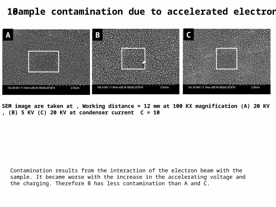
Sample contamination due to accelerated electron10
Contamination results from the interaction of the electron beam with the sample. It became worse with the increase in the accelerating voltage and the charging. Therefore B has less contamination than A and C.
BA C
SEM image are taken at , Working distance = 12 mm at 100 KX magnification (A) 20 KV , (B) 5 KV (C) 20 KV at condenser current C = 10
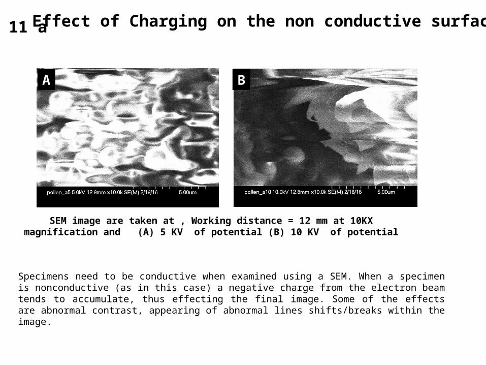
11 a Effect of Charging on the non conductive surface
Specimens need to be conductive when examined using a SEM. When a specimen is nonconductive (as in this case) a negative charge from the electron beam tends to accumulate, thus effecting the final image. Some of the effects are abnormal contrast, appearing of abnormal lines shifts/breaks within the image.
BA
SEM image are taken at , Working distance = 12 mm at 10KX magnification and (A) 5 KV of potential (B) 10 KV of potential
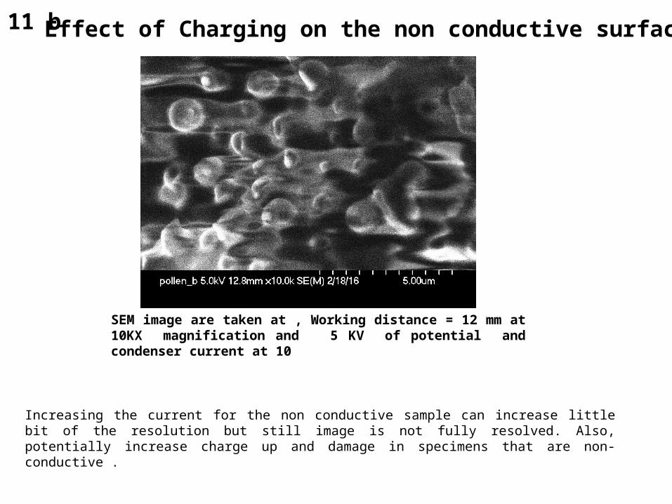
11 b
SEM image are taken at , Working distance = 12 mm at 10KX magnification and 5 KV of potential and condenser current at 10
Effect of Charging on the non conductive surface
Increasing the current for the non conductive sample can increase little bit of the resolution but still image is not fully resolved. Also, potentially increase charge up and damage in specimens that are non-conductive .
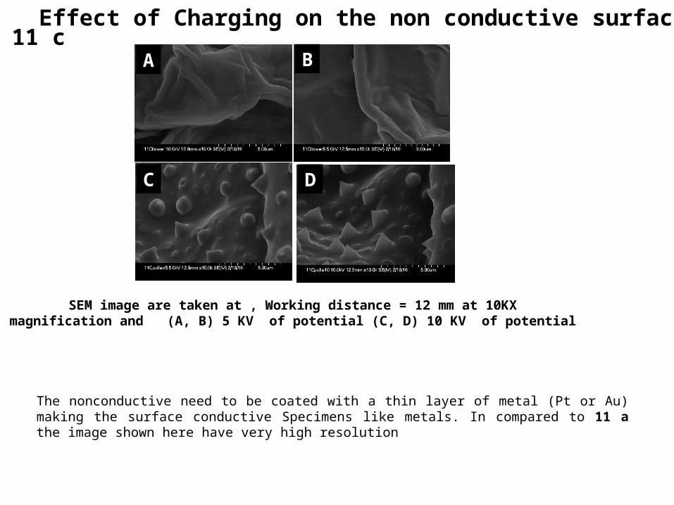
11 c
SEM image are taken at , Working distance = 12 mm at 10KX magnification and (A, B) 5 KV of potential (C, D) 10 KV of potential
The nonconductive need to be coated with a thin layer of metal (Pt or Au) making the surface conductive Specimens like metals. In compared to 11 a the image shown here have very high resolution
BA
C D
Effect of Charging on the non conductive surface