Embed Size (px)
Citation preview
1
Andrew B. Kahng
UCSD and Blaze DFM, [email protected]
Part V: Design Optimizations
2DAC-2006 DFM Tutorial: Nagaraj, Schoellkopf, Smayling, Wong, Kahng Andrew B. Kahng
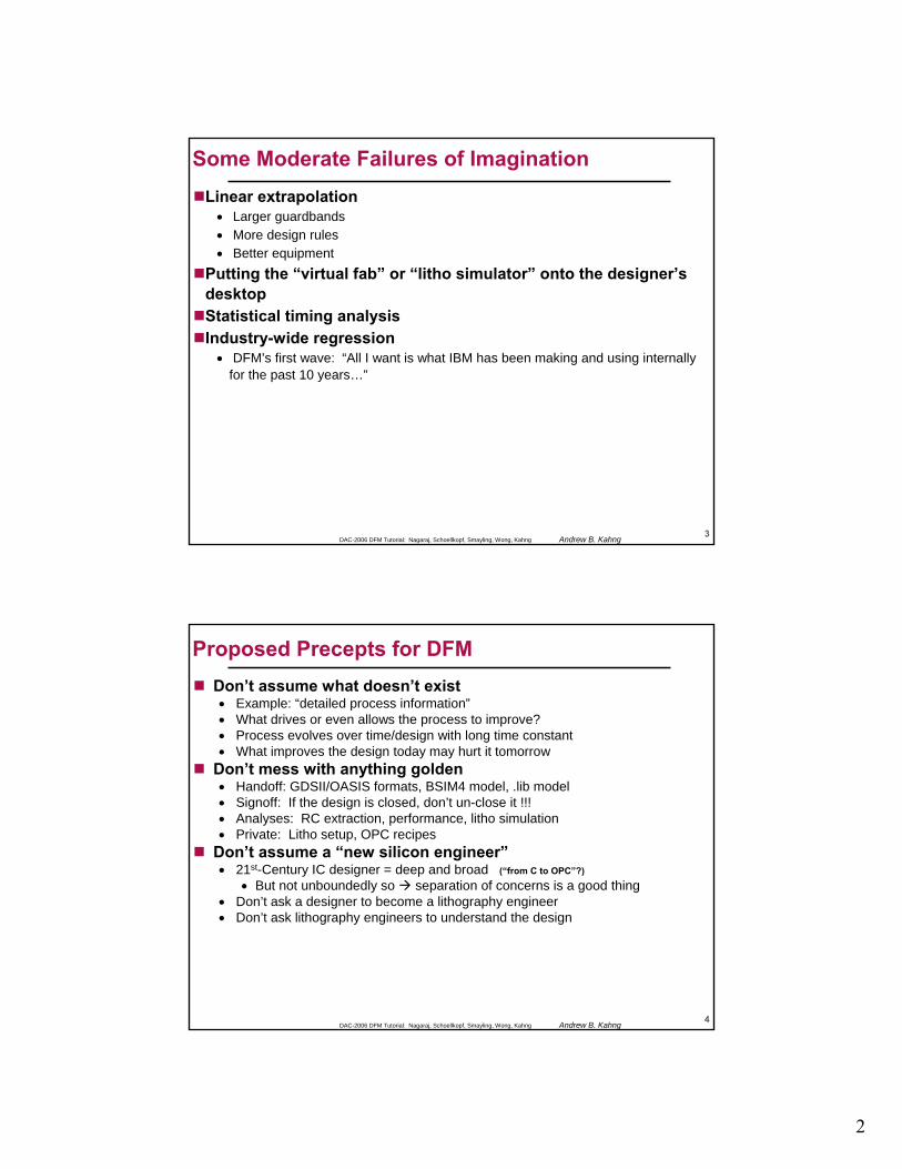
Three Trends
Trend 1: Reactions to “failure of WYSIWYG”• Shape (litho, etch) and thickness (CMP) simulators• Geometric criteria (process-window hot-spot checkers, etc.) before electrical
criteria (Iddq, FMax variation, etc.)• Library/IP development use models before full-chip use models• Analyses before optimizations
Trend 2: Reactions to “uncontrollable variation”• Experiments with statistical analysis tools
Trend 3: Commoditization of IDM internal technologies• Defect-oriented yield analyses: critical area analysis• Simple layout methodologies: post-route via/contact doubling
2
3DAC-2006 DFM Tutorial: Nagaraj, Schoellkopf, Smayling, Wong, Kahng Andrew B. Kahng
Some Moderate Failures of ImaginationLinear extrapolation
• Larger guardbands• More design rules• Better equipment
Putting the “virtual fab” or “litho simulator” onto the designer’s desktopStatistical timing analysisIndustry-wide regression
• DFM’s first wave: “All I want is what IBM has been making and using internally for the past 10 years…”
4DAC-2006 DFM Tutorial: Nagaraj, Schoellkopf, Smayling, Wong, Kahng Andrew B. Kahng
Proposed Precepts for DFMDon’t assume what doesn’t exist• Example: “detailed process information”• What drives or even allows the process to improve?• Process evolves over time/design with long time constant• What improves the design today may hurt it tomorrow
Don’t mess with anything golden• Handoff: GDSII/OASIS formats, BSIM4 model, .lib model• Signoff: If the design is closed, don’t un-close it !!!• Analyses: RC extraction, performance, litho simulation• Private: Litho setup, OPC recipes
Don’t assume a “new silicon engineer”• 21st-Century IC designer = deep and broad (“from C to OPC”?)
• But not unboundedly so separation of concerns is a good thing• Don’t ask a designer to become a lithography engineer• Don’t ask lithography engineers to understand the design
3
5DAC-2006 DFM Tutorial: Nagaraj, Schoellkopf, Smayling, Wong, Kahng Andrew B. Kahng
Where We Are Today
Huge $$$ still left on the table • “Left on table” = recoverable by improved design technology
without any process or productivity change• Many concrete examples exist !• Will recover much of this in the next 3-4 years?• Power: 0.5 x full technology node• Area: 0.3 x full technology node• Frequency: 1.0 x full technology node• Variability control: 1.0 x full technology node
Simulation- and analysis-centric “first wave” of DFM• Still has some “failures of imagination”
Near-term goals• Embrace variation and optimize parametric yield• Give clear ROI for products
6DAC-2006 DFM Tutorial: Nagaraj, Schoellkopf, Smayling, Wong, Kahng Andrew B. Kahng
Outline
Detailed Placement for Process Window EnhancementCMP Fill at 65nm and BelowAuxiliary Pattern Methodology for Cell-Based OPCCrosstalk Awareness in SSTAOther
4
7DAC-2006 DFM Tutorial: Nagaraj, Schoellkopf, Smayling, Wong, Kahng Andrew B. Kahng
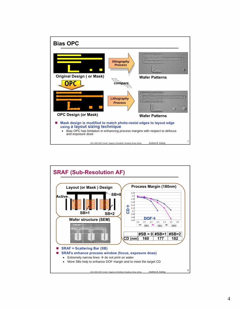
Bias OPC
Mask design is modified to match photo-resist edges to layout edge using a layout sizing technique
• Bias OPC has limitation in enhancing process margins with respect to defocus and exposure dose
Original Design ( or Mask) Wafer Patterns
OPC Design (or Mask) Wafer Patterns
OPC compare
lithography Process
LithographyProcess
8DAC-2006 DFM Tutorial: Nagaraj, Schoellkopf, Smayling, Wong, Kahng Andrew B. Kahng
SRAF (Sub-Resolution AF)
SRAF = Scattering Bar (SB)SRAFs enhance process window (focus, exposure dose)
• Extremely narrow lines do not print on water• More SBs help to enhance DOF margin and to meet the target CD
0.04
0.06
0.08
0.1
0.12
0.14
0.16
0.18
0.2
0.22
0.0 0.1 0.2 0.3 0.4 0.5 0.6
SB2 SB1 SB0
DOF
CD
SB=0
SB=2SB=1
Active
#SB = 0 #SB=1 #SB=2160 177 182CD (nm)
Layout (or Mask ) Design Process Margin (180nm)
Wafer structure (SEM)
5
9DAC-2006 DFM Tutorial: Nagaraj, Schoellkopf, Smayling, Wong, Kahng Andrew B. Kahng
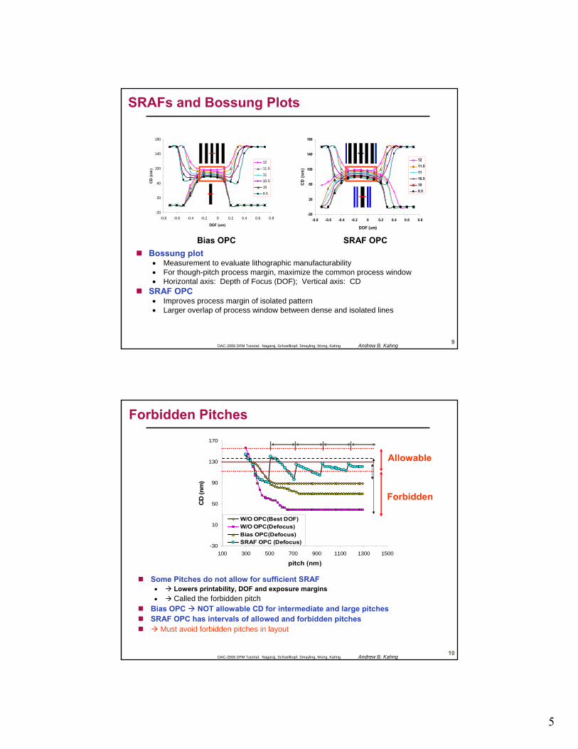
SRAFs and Bossung Plots
Bossung plot• Measurement to evaluate lithographic manufacturability • For though-pitch process margin, maximize the common process window• Horizontal axis: Depth of Focus (DOF); Vertical axis: CD
SRAF OPC • Improves process margin of isolated pattern • Larger overlap of process window between dense and isolated lines
-20
20
60
100
140
180
-0.8 -0.6 -0.4 -0.2 0 0.2 0.4 0.6 0.8
DOF (um)
CD (n
m)
1211.51110.5109.5
Bias OPC SRAF OPC
-20
20
60
100
140
180
-0.8 -0.6 -0.4 -0.2 0 0.2 0.4 0.6 0.8
DOF (um)
CD
(nm
)
1211.51110.5109.5
10DAC-2006 DFM Tutorial: Nagaraj, Schoellkopf, Smayling, Wong, Kahng Andrew B. Kahng
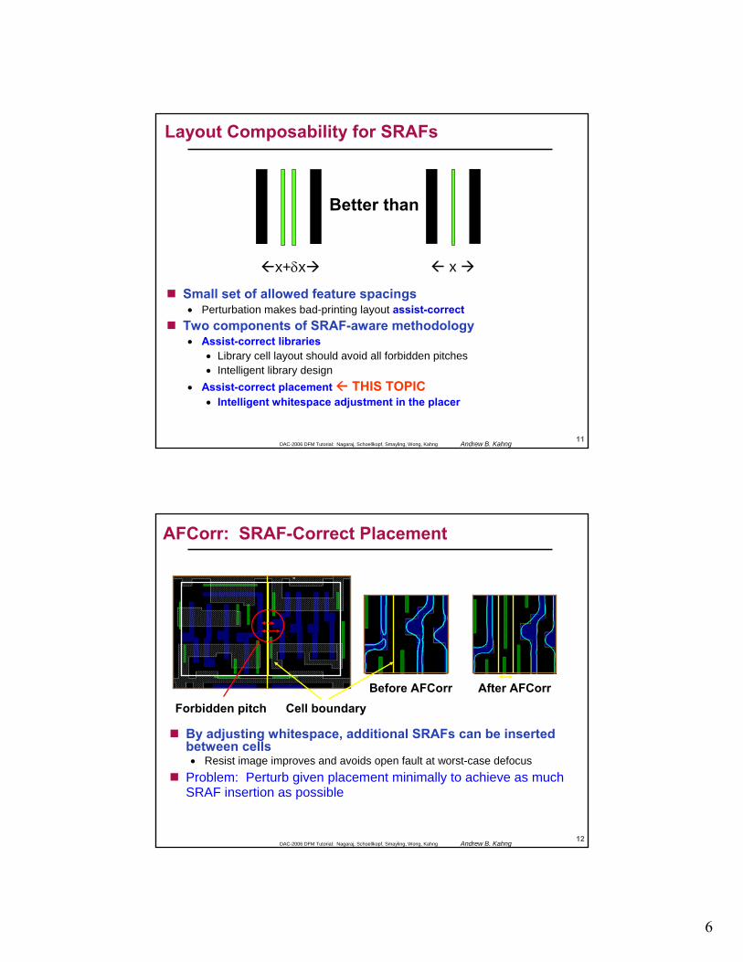
Forbidden Pitches
Some Pitches do not allow for sufficient SRAF• Lowers printability, DOF and exposure margins• Called the forbidden pitch
Bias OPC NOT allowable CD for intermediate and large pitchesSRAF OPC has intervals of allowed and forbidden pitches
Must avoid forbidden pitches in layout
-30
10
50
90
130
170
100 300 500 700 900 1100 1300 1500
pitch (nm)
CD
(nm
)
W/O OPC(Best DOF)W/O OPC(Defocus)Bias OPC(Defocus)SRAF OPC (Defocus)
#SB=1 #SB=2 #SB=3 #SB=4
Allowable
Forbidden
6
11DAC-2006 DFM Tutorial: Nagaraj, Schoellkopf, Smayling, Wong, Kahng Andrew B. Kahng
Layout Composability for SRAFs
Small set of allowed feature spacings• Perturbation makes bad-printing layout assist-correct
Two components of SRAF-aware methodology• Assist-correct libraries
• Library cell layout should avoid all forbidden pitches• Intelligent library design
• Assist-correct placement THIS TOPIC• Intelligent whitespace adjustment in the placer
x+δx x
Better than
12DAC-2006 DFM Tutorial: Nagaraj, Schoellkopf, Smayling, Wong, Kahng Andrew B. Kahng
AFCorr: SRAF-Correct Placement
By adjusting whitespace, additional SRAFs can be inserted between cells• Resist image improves and avoids open fault at worst-case defocus
Problem: Perturb given placement minimally to achieve as much SRAF insertion as possible
Cell boundaryForbidden pitchBefore AFCorr After AFCorr
7
13DAC-2006 DFM Tutorial: Nagaraj, Schoellkopf, Smayling, Wong, Kahng Andrew B. Kahng
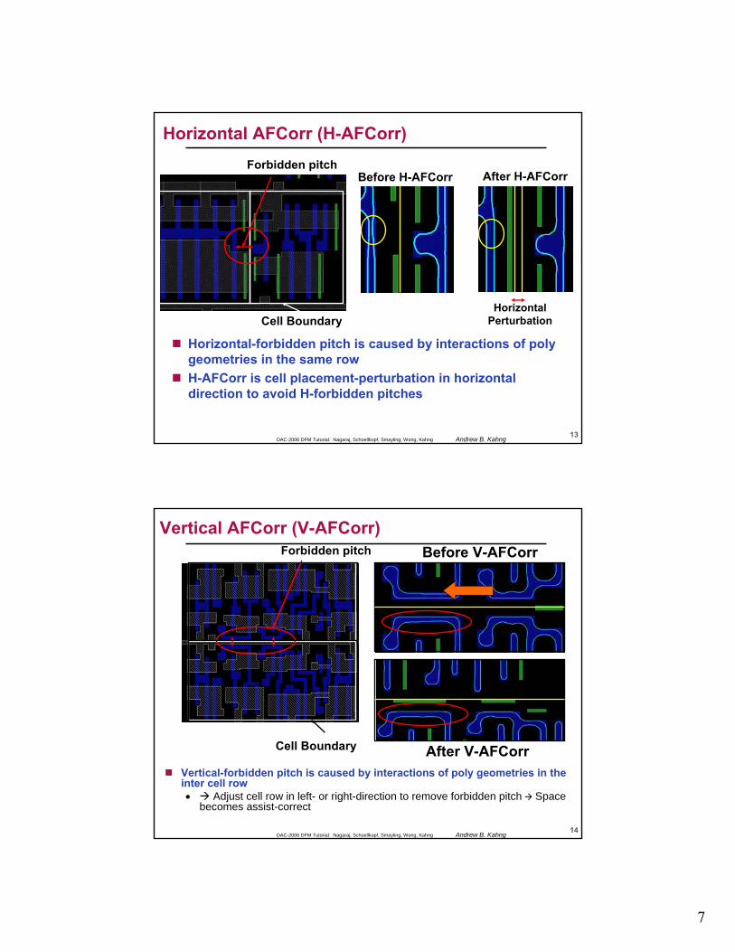
Horizontal AFCorr (H-AFCorr)
Horizontal-forbidden pitch is caused by interactions of poly geometries in the same rowH-AFCorr is cell placement-perturbation in horizontal direction to avoid H-forbidden pitches
Cell Boundary
Forbidden pitchAfter H-AFCorrBefore H-AFCorr
Horizontal Perturbation
14DAC-2006 DFM Tutorial: Nagaraj, Schoellkopf, Smayling, Wong, Kahng Andrew B. Kahng
Vertical AFCorr (V-AFCorr)
Vertical-forbidden pitch is caused by interactions of poly geometries in the inter cell row• Adjust cell row in left- or right-direction to remove forbidden pitch Space
becomes assist-correct
After V-AFCorrCell Boundary
Forbidden pitch Before V-AFCorr
8
15DAC-2006 DFM Tutorial: Nagaraj, Schoellkopf, Smayling, Wong, Kahng Andrew B. Kahng
Perturbation (H- + V- AFCorr)
AFCorr: H-AFCorr + V-AFCorr• Adjusting whitespace additional SRAFs reduce # of
forbidden pitch
AFCorr
H-AFCorr
V-AFCorr
16DAC-2006 DFM Tutorial: Nagaraj, Schoellkopf, Smayling, Wong, Kahng Andrew B. Kahng
Minimum Perturbation Approach
Objective:• Reduce forbidden pitch violation• Reduce weighted CD degradation with defocus• Minimum perturbation: preserve timing
Constraint:• Placement site width must be respected
How:• One standard cell row at a time• Solve each cell row by dynamic programming
9
17DAC-2006 DFM Tutorial: Nagaraj, Schoellkopf, Smayling, Wong, Kahng Andrew B. Kahng
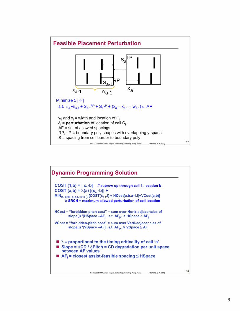
Feasible Placement Perturbation
Minimize Σ | δi |s.t. δa +δa-1 + Sa-1
RP + SaLP + (xa – xa-1 – wa-1) ∈ AF
wi and xi = width and location of Ciδi = perturbation of location of cell CiAF = set of allowed spacingsRP, LP = boundary poly shapes with overlapping y-spansS = spacing from cell border to boundary poly
XXaaxxaa--11
SSaa--11RPRP
SSaaLPLP
WWaa--11
18DAC-2006 DFM Tutorial: Nagaraj, Schoellkopf, Smayling, Wong, Kahng Andrew B. Kahng
Dynamic Programming Solution
λ = proportional to the timing criticality of cell ‘a’Slope = ∆CD / ∆Pitch = CD degradation per unit space between AF values AFi = closest assist-feasible spacing ≤ HSpace
COST (1,b) = | x1-b| // subrow up through cell 1, location bCOST (a,b) = λ(a) |(xa -b)| +MIN{Xa-SRCH ≤ i ≤ Xa+SRCH} [COST(xa-1,i) + HCost(a,b,a-1,i)+VCost(a,b)]
// SRCH = maximum allowed perturbation of cell location
HCost = “forbidden-pitch cost” = sum over Horiz-adjacencies ofslope(j) *|HSpace –AFj| s.t. AFj+1 > HSpace ≥ AFj
VCost = “forbidden-pitch cost” = sum over Verti-adjacencies ofslope(j) *|VSpace –AFj| s.t. AFj+1 > VSpace ≥ AFj
10
19DAC-2006 DFM Tutorial: Nagaraj, Schoellkopf, Smayling, Wong, Kahng Andrew B. Kahng
Experimental Setup
KLA-Tencor’s Prolith• Model generation for OPCpro
• Best focus/ worst (0.5 micron) defocus• Calculating forbidden pitches
Mentor’s OPCpro, SBar SVRF• OPC, SRAF insertion, ORC (Optical Rule Check)
Cadence SOC Encounter• Placement & Route
Synopsys Design Complier• Benchmark design ALU from OpenCore.org• Synthesis
20DAC-2006 DFM Tutorial: Nagaraj, Schoellkopf, Smayling, Wong, Kahng Andrew B. Kahng
Experimental Metrics
SB Count• Total number of scattering bars or SRAFs inserted in the design• Higher number of SRAFs indicates less through-focus variation and is
hence desirableForbidden Pitch Count • Number of border poly geometries estimated as having greater than
10% CD error through-focusEPE Count• Number of edge fragments on border poly geometries having greater
than 10% edge placement error at the worst defocus level
11
21DAC-2006 DFM Tutorial: Nagaraj, Schoellkopf, Smayling, Wong, Kahng Andrew B. Kahng
0
50000
100000
150000
200000
250000
300000
90 80 70 60 50
Utilization(%)
# To
tal S
B
0
10000
20000
30000
40000
50000
60000
70000
80000
90000
# SB
Diff
eren
ce
SB difference (130)SB difference (90)SB w/o AFCorr(130)SB w AFCorr(130)SB w/o AFCorr(90)SB w AFCorr(90)
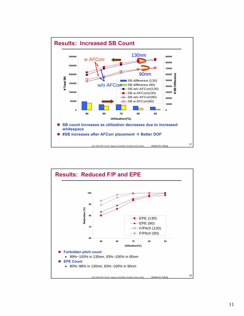
Results: Increased SB Count
SB count increases as utilization decreases due to increased whitespace#SB increases after AFCorr placement Better DOF
w AFCorr
w/o AFCorr
130nm
90nm
22DAC-2006 DFM Tutorial: Nagaraj, Schoellkopf, Smayling, Wong, Kahng Andrew B. Kahng
Results: Reduced F/P and EPE
60
70
80
90
100
90 80 70 60 50
Utilization(%)
Red
uctio
n (%
)
EPE (130)EPE (90)F/Pitch (130)F/Pitch (90)
Forbidden pitch count• 89%~100% in 130nm, 93%~100% in 90nm
EPE Count• 80%~98% in 130nm, 83%~100% in 90nm
12
23DAC-2006 DFM Tutorial: Nagaraj, Schoellkopf, Smayling, Wong, Kahng Andrew B. Kahng
Impact on Other Design Metrics
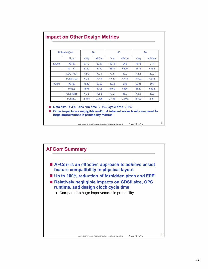
Data size 3%, OPC run time 4%, Cycle time 6%Other impacts are negligible and/or at inherent noise level, compared to large improvement in printability metrics
563255295535545150114835R/T(s)
1072131532481312627523#EPE90nm
42.242.242.341.841.942.9GDS (MB)
693268786899683967326721R/T (s)
2744976962597522678772#EPE130nm
AFCorrOrigAFCorrOrigAFCorrOrigFlow:
2.472.5222.6022.4582.3052.478Delay(s)
41.2
4.547
80
42.3
4.49
41.1
4.21
90
GDS(MB)
Delay (ns)
Utilization(%)
42.342.243.2
4.3714.5014.444
70
24DAC-2006 DFM Tutorial: Nagaraj, Schoellkopf, Smayling, Wong, Kahng Andrew B. Kahng
AFCorr Summary
AFCorr is an effective approach to achieve assist feature compatibility in physical layoutUp to 100% reduction of forbidden pitch and EPERelatively negligible impacts on GDSII size, OPC runtime, and design clock cycle time• Compared to huge improvement in printability
13
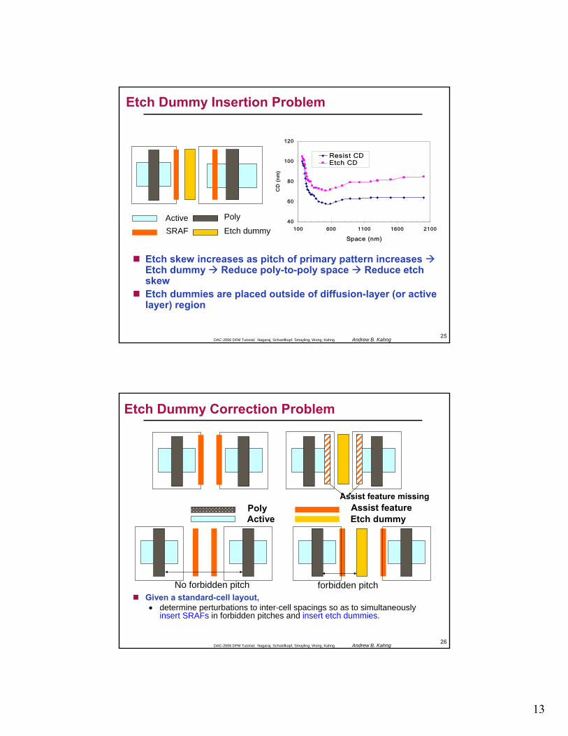
25DAC-2006 DFM Tutorial: Nagaraj, Schoellkopf, Smayling, Wong, Kahng Andrew B. Kahng
Etch Dummy Insertion Problem
Etch skew increases as pitch of primary pattern increases Etch dummy Reduce poly-to-poly space Reduce etch skewEtch dummies are placed outside of diffusion-layer (or active layer) region
40
60
80
100
120
100 600 1100 1600 2100
Space (nm)
CD
(n
m)
Resist CDEtch CD
ActiveSRAF
Poly
Etch dummy
26DAC-2006 DFM Tutorial: Nagaraj, Schoellkopf, Smayling, Wong, Kahng Andrew B. Kahng
Etch Dummy Correction Problem
Given a standard-cell layout, • determine perturbations to inter-cell spacings so as to simultaneously
insert SRAFs in forbidden pitches and insert etch dummies.
Etch dummy
Assist feature missing
No forbidden pitch forbidden pitch
Assist featureActivePoly
14
27DAC-2006 DFM Tutorial: Nagaraj, Schoellkopf, Smayling, Wong, Kahng Andrew B. Kahng
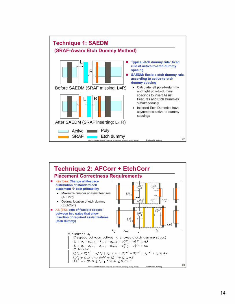
Technique 1: SAEDM(SRAF-Aware Etch Dummy Method)
Typical etch dummy rule: fixed rule of active-to-etch dummy spacingSAEDM: flexible etch dummy rule according to active-to-etch dummy spacing• Calculate left poly-to-dummy
and right poly-to-dummy spacings to insert Assist Features and Etch Dummies simultaneously
• Inserted Etch Dummies have asymmetric active-to-dummy spacings
Before SAEDM (SRAF missing: L=R)
After SAEDM (SRAF inserting: L≠ R)
L
L
R
R
ActiveSRAF
PolyEtch dummy
28DAC-2006 DFM Tutorial: Nagaraj, Schoellkopf, Smayling, Wong, Kahng Andrew B. Kahng
Technique 2: AFCorr + EtchCorr Placement Correctness RequirementsKey Idea: Change whitespace distribution of standard-cell placement best printability
• Maximize number of assist features (AFCorr)
• Optimal location of etch dummy (EtchCorr)
AS (ES): sets of feasible spaces between two gates that allow insertion of required assist features (etch dummy)
15
29DAC-2006 DFM Tutorial: Nagaraj, Schoellkopf, Smayling, Wong, Kahng Andrew B. Kahng
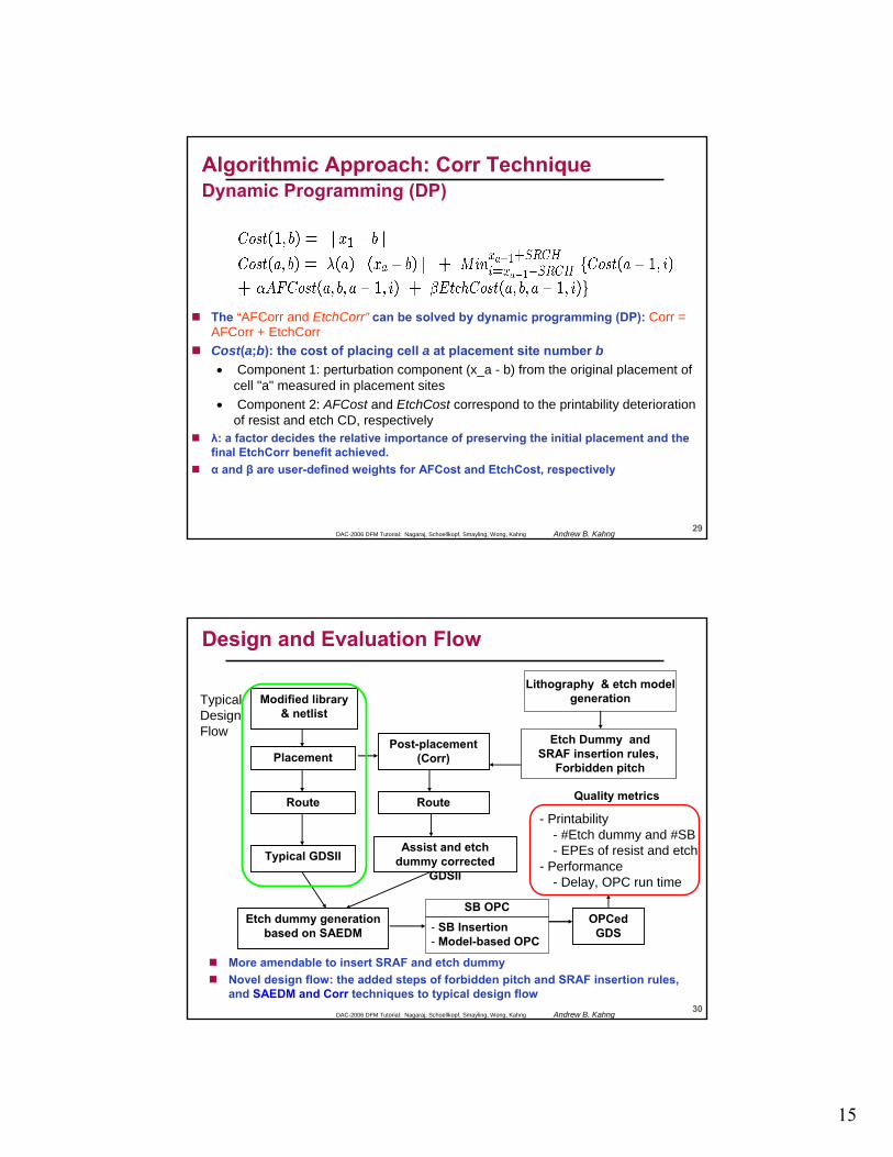
Algorithmic Approach: Corr Technique Dynamic Programming (DP)
The “AFCorr and EtchCorr” can be solved by dynamic programming (DP): Corr = AFCorr + EtchCorrCost(a;b): the cost of placing cell a at placement site number b• Component 1: perturbation component (x_a - b) from the original placement of
cell "a" measured in placement sites• Component 2: AFCost and EtchCost correspond to the printability deterioration
of resist and etch CD, respectivelyλ: a factor decides the relative importance of preserving the initial placement and the final EtchCorr benefit achieved. α and β are user-defined weights for AFCost and EtchCost, respectively
30DAC-2006 DFM Tutorial: Nagaraj, Schoellkopf, Smayling, Wong, Kahng Andrew B. Kahng
Design and Evaluation Flow
TypicalDesign Flow Etch Dummy and
SRAF insertion rules,Forbidden pitch
SB OPC- SB Insertion- Model-based OPC
Lithography & etch modelgenerationModified library
& netlist
Placement
Assist and etch dummy corrected
GDSII
Route
Typical GDSII
Route
Post-placement(Corr)
OPCed GDS
Etch dummy generation based on SAEDM
- Printability- #Etch dummy and #SB- EPEs of resist and etch
- Performance- Delay, OPC run time
Quality metrics
More amendable to insert SRAF and etch dummyNovel design flow: the added steps of forbidden pitch and SRAF insertion rules, and SAEDM and Corr techniques to typical design flow
16
31DAC-2006 DFM Tutorial: Nagaraj, Schoellkopf, Smayling, Wong, Kahng Andrew B. Kahng
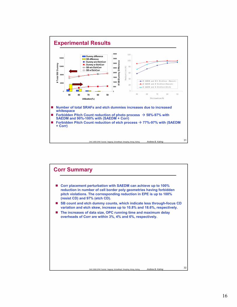
Experimental Results
0
40000
80000
120000
160000
90 80 70 60 50
Utilization(%)
# To
tal S
B/ D
umm
y
0
5000
10000
15000
20000
25000
30000
35000
40000
# SB
/Dum
my
Diff
eren
ce
Dummy differenceSB differenceDummy w/o EtchCorrDummy w EtchCorrSB w/o EtchCorrSB w EtchCorr
0
20
40
60
80
100
120
90 80 70 60 50
Utilization(%)
Redu
ctio
n(%
)
W SAEDM and W/O EtchCorr (Resist)
W SAEDM and W EtchCorr(Resist)
W SAEDM and W EtchCorr(Etch)
Number of total SRAFs and etch dummies increases due to increased whitespaceForbidden Pitch Count reduction of photo process 58%-97% with SAEDM and 90%-100% with (SAEDM + Corr)Forbidden Pitch Count reduction of etch process 77%-97% with (SAEDM + Corr)
32DAC-2006 DFM Tutorial: Nagaraj, Schoellkopf, Smayling, Wong, Kahng Andrew B. Kahng
Corr Summary
Corr placement perturbation with SAEDM can achieve up to 100% reduction in number of cell border poly geometries having forbidden pitch violations. The corresponding reduction in EPE is up to 100% (resist CD) and 97% (etch CD).SB count and etch dummy counts, which indicate less through-focus CD variation and etch skew, increase up to 10.8% and 18.6%, respectively. The increases of data size, OPC running time and maximum delay overheads of Corr are within 3%, 4% and 6%, respectively.
17
33DAC-2006 DFM Tutorial: Nagaraj, Schoellkopf, Smayling, Wong, Kahng Andrew B. Kahng
Outline
Detailed Placement for Process Window EnhancementCMP Fill at 65nm and BelowAuxiliary Pattern Methodology for Cell-Based OPCCrosstalk Awareness in SSTAOther
34DAC-2006 DFM Tutorial: Nagaraj, Schoellkopf, Smayling, Wong, Kahng Andrew B. Kahng
BEOL Contribution to Variation
Scalable optimal CMP fill (metal, STI, timing, fill pattern)Combinatorial methods for redundant via insertion“Religious questions”
± 5%Model/hardware uncertainty (Per cell type)
±10%N/P mistrack(Fast rise/slow fall, fast fall/slow rise)
±10%Device fatigue (NBTI, hot electron effects)
±10%PLL (Jitter, duty cycle, phase error)
± 5%Vt and Tox device family tracking (Can have multiple Vt and Tox device families)
±15 %Environmental (Voltage islands, IR drop, temperature)
-10% → +25%BEOL metal (Metal mistrack, thin/thick wires)
Delay ImpactParameter
18
35DAC-2006 DFM Tutorial: Nagaraj, Schoellkopf, Smayling, Wong, Kahng Andrew B. Kahng
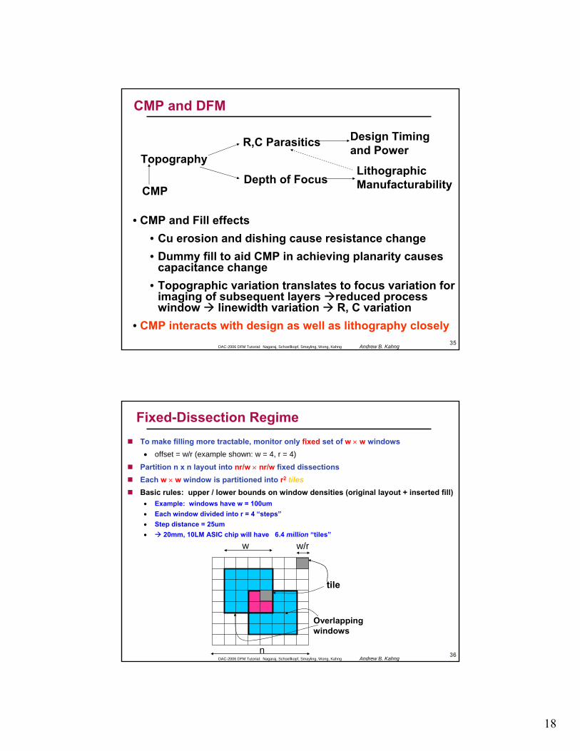
CMP and DFM
TopographyR,C Parasitics Design Timing
and Power
Depth of FocusLithographicManufacturabilityCMP
• CMP and Fill effects• Cu erosion and dishing cause resistance change• Dummy fill to aid CMP in achieving planarity causes
capacitance change• Topographic variation translates to focus variation for
imaging of subsequent layers reduced process window linewidth variation R, C variation
• CMP interacts with design as well as lithography closely
36DAC-2006 DFM Tutorial: Nagaraj, Schoellkopf, Smayling, Wong, Kahng Andrew B. Kahng
Fixed-Dissection RegimeTo make filling more tractable, monitor only fixed set of w × w windows
• offset = w/r (example shown: w = 4, r = 4)
Partition n x n layout into nr/w × nr/w fixed dissectionsEach w × w window is partitioned into r2 tilesBasic rules: upper / lower bounds on window densities (original layout + inserted fill)
• Example: windows have w = 100um• Each window divided into r = 4 “steps”• Step distance = 25um• 20mm, 10LM ASIC chip will have 6.4 million “tiles”
w/r
Overlapping windows
w
n
tile
19
37DAC-2006 DFM Tutorial: Nagaraj, Schoellkopf, Smayling, Wong, Kahng Andrew B. Kahng
Previous / New Objectives in Density Control
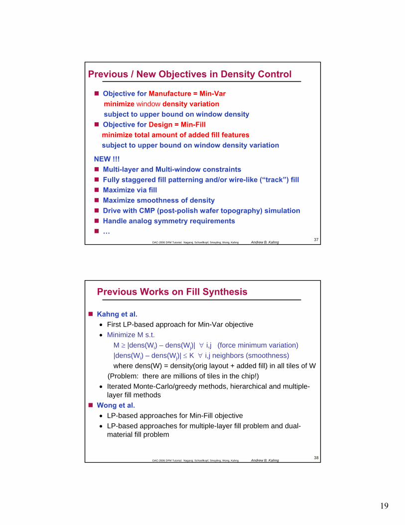
Objective for Manufacture = Min-Varminimize window density variationsubject to upper bound on window densityObjective for Design = Min-Fillminimize total amount of added fill featuressubject to upper bound on window density variation
NEW !!!Multi-layer and Multi-window constraintsFully staggered fill patterning and/or wire-like (“track”) fillMaximize via fillMaximize smoothness of densityDrive with CMP (post-polish wafer topography) simulationHandle analog symmetry requirements…
38DAC-2006 DFM Tutorial: Nagaraj, Schoellkopf, Smayling, Wong, Kahng Andrew B. Kahng
Previous Works on Fill Synthesis
Kahng et al. • First LP-based approach for Min-Var objective• Minimize M s.t.
M ≥ |dens(Wi) – dens(Wj)| ∀ i,j (force minimum variation)|dens(Wi) – dens(Wj)| ≤ K ∀ i,j neighbors (smoothness)where dens(W) = density(orig layout + added fill) in all tiles of W
(Problem: there are millions of tiles in the chip!)• Iterated Monte-Carlo/greedy methods, hierarchical and multiple-
layer fill methodsWong et al.• LP-based approaches for Min-Fill objective• LP-based approaches for multiple-layer fill problem and dual-
material fill problem
20
39DAC-2006 DFM Tutorial: Nagaraj, Schoellkopf, Smayling, Wong, Kahng Andrew B. Kahng
What Would “Optimum” CMP Fill Look Like?
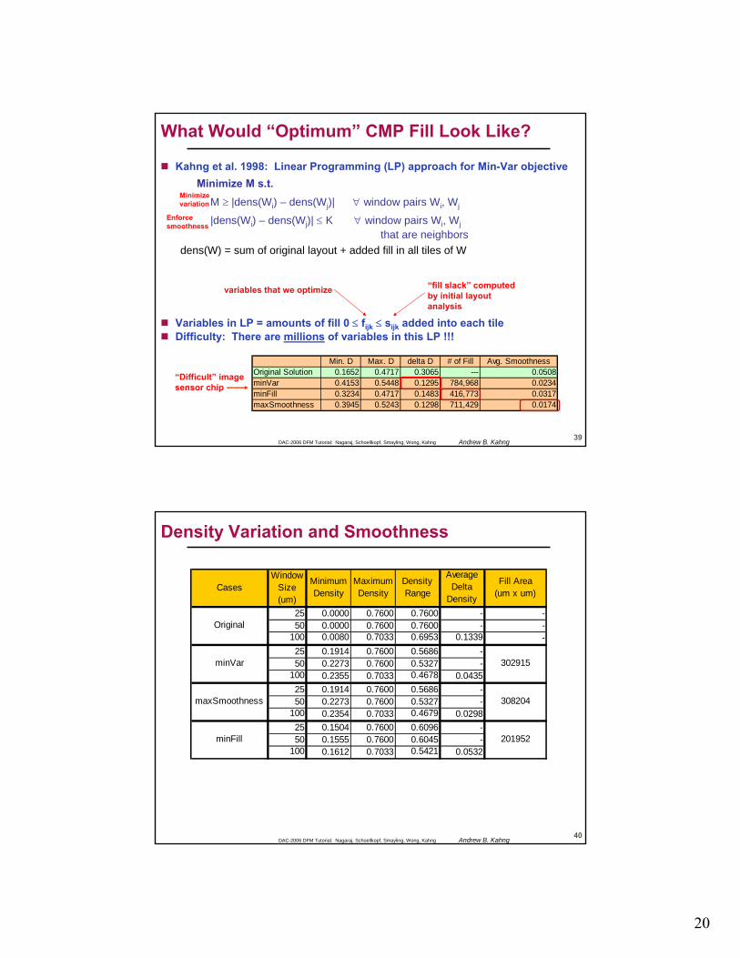
Kahng et al. 1998: Linear Programming (LP) approach for Min-Var objectiveMinimize M s.t.
M ≥ |dens(Wi) – dens(Wj)| ∀ window pairs Wi, Wj
|dens(Wi) – dens(Wj)| ≤ K ∀ window pairs Wi, Wjthat are neighbors
dens(W) = sum of original layout + added fill in all tiles of W
Variables in LP = amounts of fill 0 ≤ fijk ≤ sijk added into each tileDifficulty: There are millions of variables in this LP !!!
Minimize variation
Enforce smoothness
“fill slack” computed by initial layout analysis
variables that we optimize
Min. D Max. D delta D # of Fill Avg. SmoothnessOriginal Solution 0.1652 0.4717 0.3065 --- 0.0508minVar 0.4153 0.5448 0.1295 784,968 0.0234minFill 0.3234 0.4717 0.1483 416,773 0.0317maxSmoothness 0.3945 0.5243 0.1298 711,429 0.0174
“Difficult” image sensor chip
40DAC-2006 DFM Tutorial: Nagaraj, Schoellkopf, Smayling, Wong, Kahng Andrew B. Kahng
Density Variation and Smoothness
Smoothness
Variation
CasesWindow
Size (um)
Minimum Density
Maximum Density
Density Range
Average Delta
Density
Fill Area (um x um)
25 0.0000 0.7600 0.7600 - -50 0.0000 0.7600 0.7600 - -
100 0.0080 0.7033 0.6953 0.1339 -25 0.1914 0.7600 0.5686 -50 0.2273 0.7600 0.5327 -
100 0.2355 0.7033 0.4678 0.043525 0.1914 0.7600 0.5686 -50 0.2273 0.7600 0.5327 -
100 0.2354 0.7033 0.4679 0.029825 0.1504 0.7600 0.6096 -50 0.1555 0.7600 0.6045 -
100 0.1612 0.7033 0.5421 0.0532
302915
201952
308204
Original
minVar
maxSmoothness
minFill

21
41DAC-2006 DFM Tutorial: Nagaraj, Schoellkopf, Smayling, Wong, Kahng Andrew B. Kahng
Religious Questions in BEOL DFMShould CMP fill be owned by the routing / timing closure tool orby the DRC / PG tool?• Answer: proper fill is best achieved today post-layout by a tool that maintains
the signoff
Must fill be “timing-driven”, or is “timing-aware” sufficient?• Answer: “Timing-aware” is likely sufficient through the 45nm node
Are CMP and litho simulations for “more accurate parasiticsand signoff” really necessary?• Answer: Probably not. CDs and thickness variations are “self-compensating”
w.r.t. timing. Guardbands are reasonable. There is a big mess with existing calibrations of the RC extraction tool to silicon.
If two solutions both meet the spec, are they of equal value?How elaborate must cost functions and layout knobs be for EDA tools to understand via yield / reliability, EM, etc.?...
42DAC-2006 DFM Tutorial: Nagaraj, Schoellkopf, Smayling, Wong, Kahng Andrew B. Kahng
“Intelligent” Fill Goals for 65nm and beyondTrue timing- and SI-awareness• Driven by internal engines for incremental extraction, delay calculation,
static timing/noise analysis• Open Question: is this done by the router? Or post-layout processing?
True multi-layer, multi-window global optimization of effective density smoothness and uniformity• Recall: millions of “tiles” – can we optimize all fill on all layers
simultaneously?
Analog fill, capacitor fill, via fillFloating, grounded and track fillStandalone, ECO, and ripup-refill use modelsSupports thickness bias models (CMP predictors)Key technology for managing BEOL variability and enhancing parametric yield
22
43DAC-2006 DFM Tutorial: Nagaraj, Schoellkopf, Smayling, Wong, Kahng Andrew B. Kahng
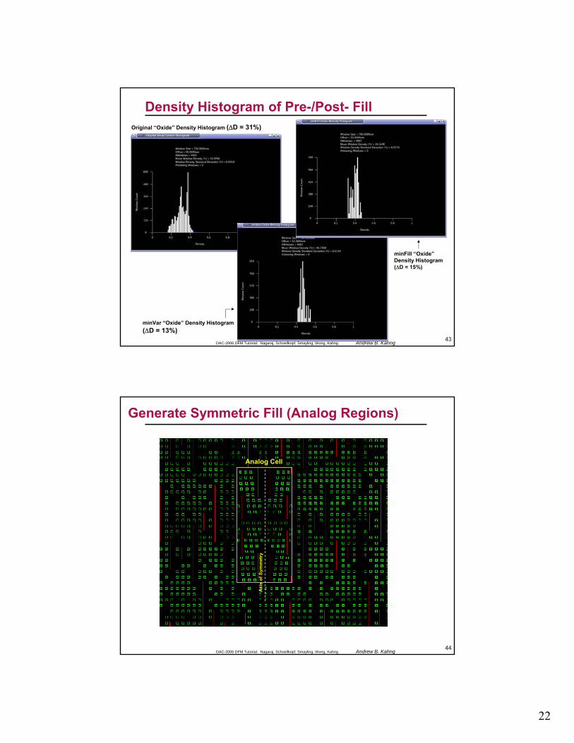
Density Histogram of Pre-/Post- FillOriginal “Oxide” Density Histogram (∆D = 31%)
minVar “Oxide” Density Histogram(∆D = 13%)
minFill “Oxide”Density Histogram(∆D = 15%)
44DAC-2006 DFM Tutorial: Nagaraj, Schoellkopf, Smayling, Wong, Kahng Andrew B. Kahng
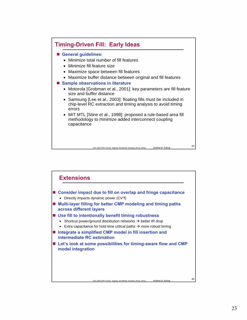
Analog Cell
Axi
s of
Sym
met
ry
Generate Symmetric Fill (Analog Regions)
23
45DAC-2006 DFM Tutorial: Nagaraj, Schoellkopf, Smayling, Wong, Kahng Andrew B. Kahng
Timing-Driven Fill: Early IdeasGeneral guidelines:• Minimize total number of fill features• Minimize fill feature size• Maximize space between fill features• Maximize buffer distance between original and fill features
Sample observations in literature• Motorola [Grobman et al., 2001]: key parameters are fill feature
size and buffer distance• Samsung [Lee et al., 2003]: floating fills must be included in
chip-level RC extraction and timing analysis to avoid timing errors
• MIT MTL [Stine et al., 1998]: proposed a rule-based area fill methodology to minimize added interconnect coupling capacitance
46DAC-2006 DFM Tutorial: Nagaraj, Schoellkopf, Smayling, Wong, Kahng Andrew B. Kahng
Extensions
Consider impact due to fill on overlap and fringe capacitance• Directly impacts dynamic power (CV2f)
Multi-layer filling for better CMP modeling and timing paths across different layersUse fill to intentionally benefit timing robustness • Shortcut power/ground distribution networks better IR drop• Extra capacitance for hold time critical paths more robust timing
Integrate a simplified CMP model in fill insertion and intermediate RC estimationLet’s look at some possibilities for timing-aware flow and CMP model integration
24
47DAC-2006 DFM Tutorial: Nagaraj, Schoellkopf, Smayling, Wong, Kahng Andrew B. Kahng
Intelligent Fill
Timing-Aware and Timing-Driven Use Models
External CMP
Model
GDSTopoMap
SPEF, SDCSI / Timing reportsList of critical nets
GDS / LEF/DEF / OATech file / DRM
User parameters
GDS’ / DEF’ / OA’
ReportsSPEF’
(to signoff analyses)
P&R (ECO)
Intelligent Fill (ECO)
RCX
SI / Timing
DEF’ / DB’ (or, GDS)
DEF / DB
Timing-Aware = Timing-Driven = +
48DAC-2006 DFM Tutorial: Nagaraj, Schoellkopf, Smayling, Wong, Kahng Andrew B. Kahng
Critical Net File Example
MULT.C[46] { M1 M1 1.4 \M1 M2 1.12 \M2 M1 1.12 \M2 M2 1.4 \M2 M3 1.12 \M3 M2 1.12 \M3 M3 1.4 \M3 M4 1.12 \M4 M3 1.12 \M4 M4 1.4 \M4 M5 1.12 \M5 M4 1.12 \M5 M5 1.4 \M5 M6 1.12 \M6 M5 1.12 \M6 M6 1.4 \M6 M1_2B 2.24 \M1_2B M6 2.24 \M1_2B M1_2B 2.8 \M1_2B M2_2B 2.24 \M2_2B M1_2B 2.24 \M2_2B M2_2B 2.8 \
}…
For each of the top K critical nets, e.g., block out areas in:
(1) layer below the net(2) layer of the net(3) layer above the net
For a net segment in M3, block 1.12um from the segment in M2.
25
49DAC-2006 DFM Tutorial: Nagaraj, Schoellkopf, Smayling, Wong, Kahng Andrew B. Kahng
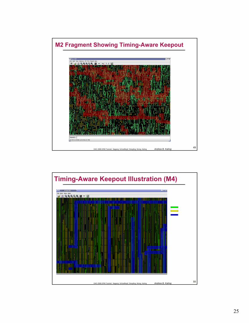
M2 Fragment Showing Timing-Aware Keepout
50DAC-2006 DFM Tutorial: Nagaraj, Schoellkopf, Smayling, Wong, Kahng Andrew B. Kahng
Timing-Aware Keepout Illustration (M4)
M4 routeM4 fillM4 keepout
26
51DAC-2006 DFM Tutorial: Nagaraj, Schoellkopf, Smayling, Wong, Kahng Andrew B. Kahng
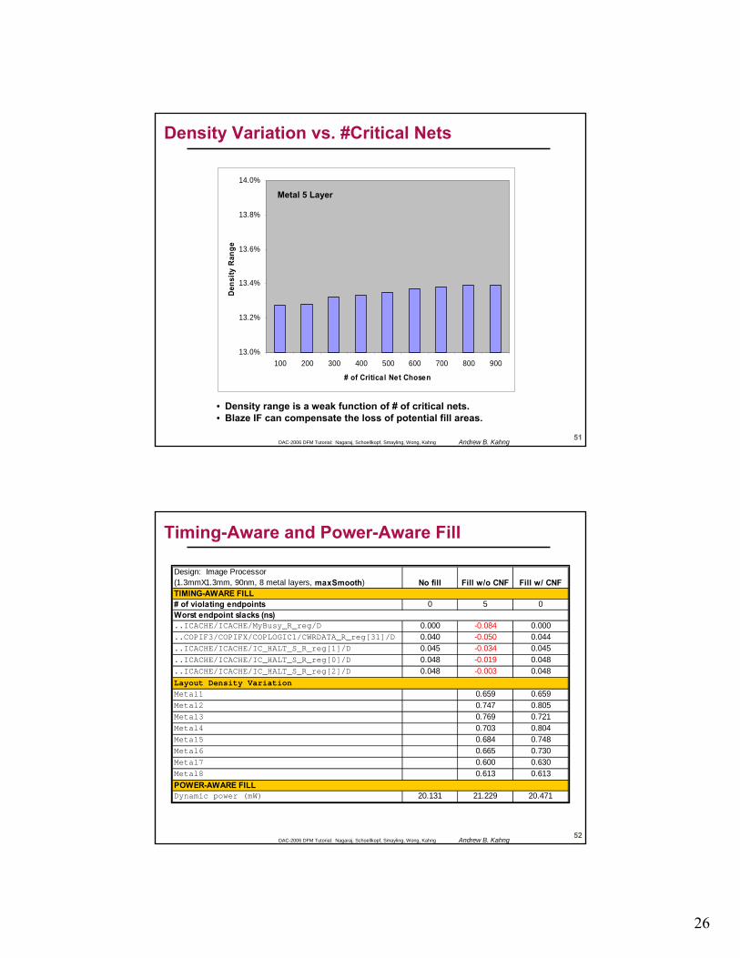
Density Variation vs. #Critical Nets
13.0%
13.2%
13.4%
13.6%
13.8%
14.0%
100 200 300 400 500 600 700 800 900
# of Critical Net Chosen
Dens
ity R
ange
• Density range is a weak function of # of critical nets.• Blaze IF can compensate the loss of potential fill areas.
Metal 5 Layer
52DAC-2006 DFM Tutorial: Nagaraj, Schoellkopf, Smayling, Wong, Kahng Andrew B. Kahng
Timing-Aware and Power-Aware Fill
Design: Image Processor (1.3mmX1.3mm, 90nm, 8 metal layers, maxSmooth) No fill Fill w/o CNF Fill w/ CNF
# of violating endpoints 0 5 0
..ICACHE/ICACHE/MyBusy_R_reg/D 0.000 -0.084 0.000
..COPIF3/COPIFX/COPLOGIC1/CWRDATA_R_reg[31]/D 0.040 -0.050 0.044
..ICACHE/ICACHE/IC_HALT_S_R_reg[1]/D 0.045 -0.034 0.045
..ICACHE/ICACHE/IC_HALT_S_R_reg[0]/D 0.048 -0.019 0.048
..ICACHE/ICACHE/IC_HALT_S_R_reg[2]/D 0.048 -0.003 0.048
Metal1 0.659 0.659Metal2 0.747 0.805Metal3 0.769 0.721Metal4 0.703 0.804Metal5 0.684 0.748Metal6 0.665 0.730Metal7 0.600 0.630Metal8 0.613 0.613
Dynamic power (mW) 20.131 21.229 20.471
TIMING-AWARE FILL
POWER-AWARE FILL
Layout Density Variation
Worst endpoint slacks (ns)
27
53DAC-2006 DFM Tutorial: Nagaraj, Schoellkopf, Smayling, Wong, Kahng Andrew B. Kahng
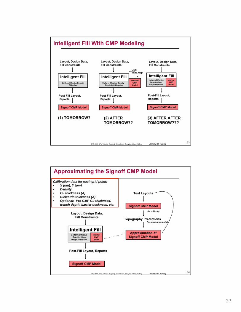
Intelligent Fill
Intelligent Fill With CMP Modeling
External CMP
Model
Intelligent Fill
Layout, Design Data, Fill Constraints
Post-Fill Layout, Reports
Signoff CMP Model
GDS,Topo Map
Internal CMP
Model
Layout, Design Data, Fill Constraints
Post-Fill Layout, Reports
Signoff CMP Model
Uniform Effective Density + Step Height Objective
Uniform Effective Density +Step
Height Objective
Intelligent Fill
Layout, Design Data, Fill Constraints
Post-Fill Layout, Reports
Signoff CMP Model
Uniform Effective Density Objective
(1) TOMORROW? (2) AFTER TOMORROW??
(3) AFTER AFTERTOMORROW???
54DAC-2006 DFM Tutorial: Nagaraj, Schoellkopf, Smayling, Wong, Kahng Andrew B. Kahng
Approximating the Signoff CMP Model
Intelligent FillInternal
CMP Model
Layout, Design Data, Fill Constraints
Post-Fill Layout, Reports
Signoff CMP Model
Uniform Effective Density +Step
Height Objective
Test Layouts
Signoff CMP Model
Topography Predictions
(or silicon)
(or measurements)
Approximation of Signoff CMP Model
Calibration data for each grid point:• X (um), Y (um)• Density• Cu thickness (A)• Dielectric thickness (A)• Optional: Pre-CMP Cu thickness,
trench depth, barrier thickness, etc.
28
55DAC-2006 DFM Tutorial: Nagaraj, Schoellkopf, Smayling, Wong, Kahng Andrew B. Kahng
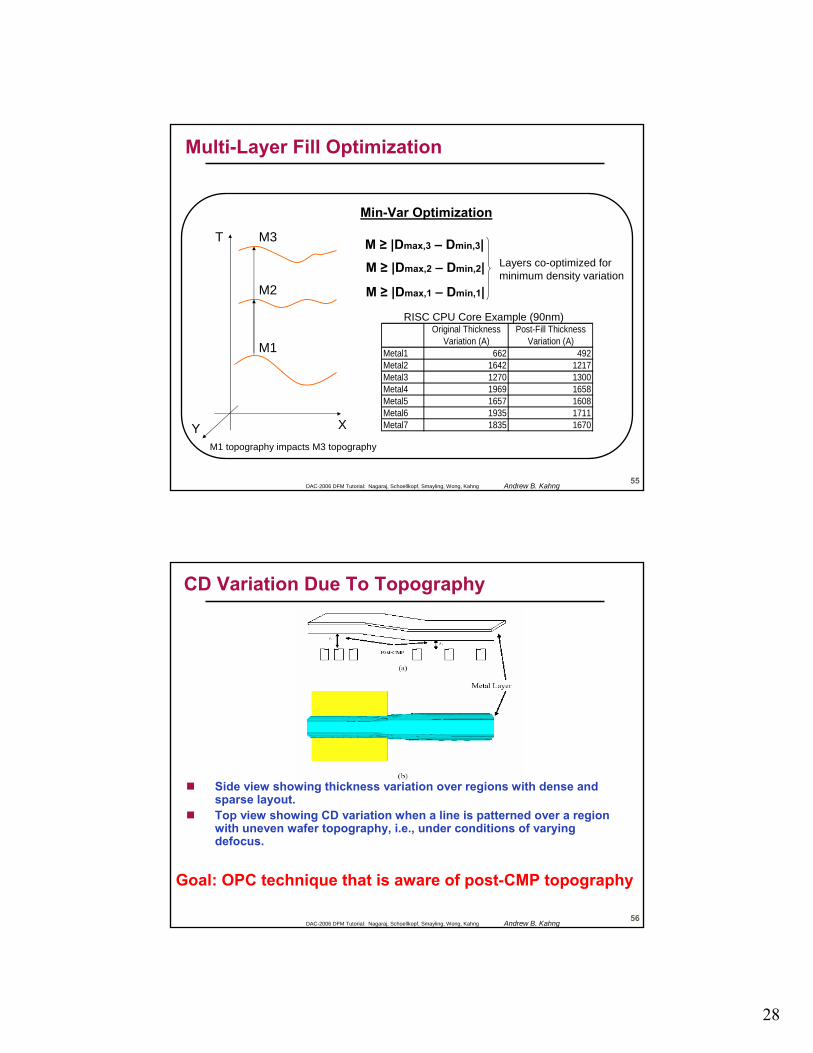
Multi-Layer Fill Optimization
M1
M2
M3T
XY
Min-Var Optimization
M ≥ |Dmax,3 – Dmin,3|
M ≥ |Dmax,2 – Dmin,2|
M ≥ |Dmax,1 – Dmin,1|
Layers co-optimized for minimum density variation
M1 topography impacts M3 topography
RISC CPU Core Example (90nm)Original Thickness
Variation (A)Post-Fill Thickness
Variation (A)Metal1 662 492Metal2 1642 1217Metal3 1270 1300Metal4 1969 1658Metal5 1657 1608Metal6 1935 1711Metal7 1835 1670
56DAC-2006 DFM Tutorial: Nagaraj, Schoellkopf, Smayling, Wong, Kahng Andrew B. Kahng
CD Variation Due To Topography
Side view showing thickness variation over regions with dense and sparse layout. Top view showing CD variation when a line is patterned over a region with uneven wafer topography, i.e., under conditions of varying defocus.
Goal: OPC technique that is aware of post-CMP topography
29
57DAC-2006 DFM Tutorial: Nagaraj, Schoellkopf, Smayling, Wong, Kahng Andrew B. Kahng
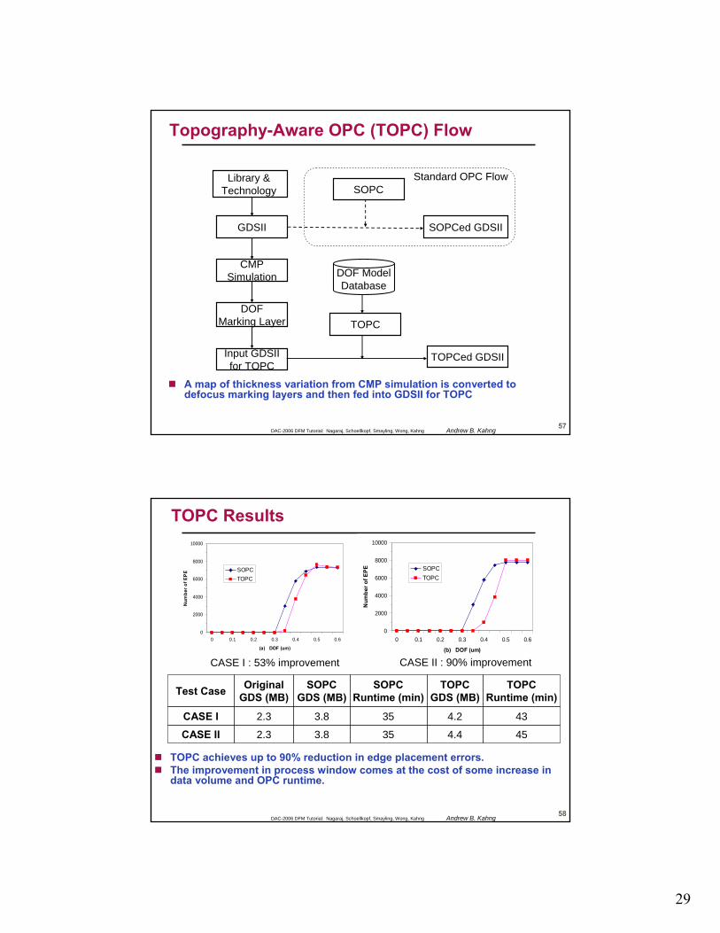
CMPSimulation
DOFMarking Layer
Library & Technology
GDSII
Input GDSIIfor TOPC
TOPCed GDSII
DOF ModelDatabase
TOPC
SOPC
SOPCed GDSII
Standard OPC Flow
Topography-Aware OPC (TOPC) Flow
A map of thickness variation from CMP simulation is converted todefocus marking layers and then fed into GDSII for TOPC
58DAC-2006 DFM Tutorial: Nagaraj, Schoellkopf, Smayling, Wong, Kahng Andrew B. Kahng
TOPC Results
TOPC achieves up to 90% reduction in edge placement errors.The improvement in process window comes at the cost of some increase in data volume and OPC runtime.
0
2000
4000
6000
8000
10000
0 0.1 0.2 0.3 0.4 0.5 0.6
(b) DOF (um)
Num
ber o
f EPE SOPC
TOPC
0
2000
4000
6000
8000
10000
0 0.1 0.2 0.3 0.4 0.5 0.6
(a) DOF (um)
Num
ber o
f EP
E SOPCTOPC
OriginalGDS (MB)
SOPCGDS (MB)
SOPCRuntime (min)Test Case TOPC
GDS (MB)TOPC
Runtime (min)
CASE I 2.3 3.8 35 4.2 43
4.4 45CASE II 2.3 3.8 35
CASE I : 53% improvement CASE II : 90% improvement
30
59DAC-2006 DFM Tutorial: Nagaraj, Schoellkopf, Smayling, Wong, Kahng Andrew B. Kahng
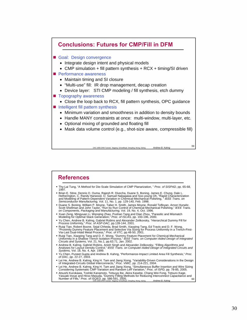
Conclusions: Futures for CMP/Fill in DFM
Goal: Design convergence• Integrate design intent and physical models• CMP simulation + fill pattern synthesis + RCX + timing/SI driven
Performance awareness• Maintain timing and SI closure• “Multi-use” fill: IR drop management, decap creation• Device layer: STI CMP modeling / fill synthesis, etch dummy
Topography awareness• Close the loop back to RCX, fill pattern synthesis, OPC guidance
Intelligent fill pattern synthesis• Minimum variation and smoothness in addition to density bounds• Handle MANY constraints at once: multi-window, multi-layer, etc.• Optional mixing of grounded and floating fill• Mask data volume control (e.g., shot-size aware, compressible fill)
60DAC-2006 DFM Tutorial: Nagaraj, Schoellkopf, Smayling, Wong, Kahng Andrew B. Kahng
Thy-Lai Tung, “A Method for Die-Scale Simulation of CMP Planarization, ” Proc. of SISPAD, pp. 65-68, 1997.Brian E. Stine, Dennis O. Ouma, Rajesh R. Divecha, Duane S. Boning, James E. Chung, Dale L. Hetherington, C. Randy Harwood, O. Samuel Nakagawa and Soo-young Oh, “Rapid Characterization and Modeling of Pattern-Dependent Variation in Chemical-Mechanical Polishing, ” IEEE Trans. on Semiconductor Manufacturing, Vol. 11, No. 1, pp. 129-140, Feb. 1998.Duane S. Boning, William P. Moyne, Taber H. Smith, James Moyne, Ronald Telfeyan, Arnon Hurwitz, Scott Shellman and John Taylor, “Run by Run Control of Chemical-Mechanical Polishing,” IEEE Trans. on Components, Packaging and Manufacturing, Vol. 19, No. 4, Oct. 1996.Xuan Zeng, Mingyuan Li, Wenqing Zhao, Pushan Tang and Dian Zhou, “Parasitic and Mismatch Modeling for Optimal Stack Generation,” Proc. of ISCAS, pp. 193-196, 2000.Yu Chen, Andrew B. Kahng, Gabriel Robins and Alexander Zelikovsky, “Hierarchical Dummy Fill for Process Uniformity,” Proc. of ASP-DAC, pp.139-144, 2001.Ruiqi Tian, Robert Boone, Sejal Chheda, Brad Smith, Xiaoping Tang, Ed Travis and D. F. Wong, “Proximity Dummy Feature Placement and Selective Via Sizing for Process Uniformity in a Trench-First-Via-Last Dual-Inlaid Metal Process,” Proc. of IITC, pp.48-50, 2001.Ruiqi Tian, Xiaoping Tang and D. F. Wong, “Dummy Feature Placement for Chemical-Mechanical Uniformity in a Shallow Trench Isolation Process,” IEEE Trans. on Computer-Aided Design of Integrated Circuits and Systems, Vol. 21, No.1, pp.63.71, Jan. 2002.Andrew B. Kahng, Gabriel Robins, Anish Singh and Alexander Zelikovsky, “Filling Algorithms and Analyses for Layout Density Control,” IEEE Trans. on Computer-Aided Design of Integrated Circuits and Systems, Vol. 18, No. 4, Apr. 1999.Yu Chen, Puneet Gupta and Andrew B. Kahng, “Performance-Impact Limited Area Fill Synthesis,” Proc. of DAC, pp. 22-27, 2003.Lei He, Andrew B. Kahng, King H. Tam and Jiang Xiong, “Variability-Driven Considerations in the Design of Integrated-Circuits Global Interconnects,” Proc. VMIC, pp. 214-221, 2004.Lei He, Andrew B. Kahng, King H. Tam and Jiang Xiong, “Simultaneous Buffer Insertion and Wire Sizing Considering Systematic CMP Variation and Random Leff Variation,” Proc. of ISPD, pp. 78-85, 2005.Atsushi Kurokawa, Toshiki Kanamoto, Tetsuya Ibe, Akira Kasebe, Chang Wei Fong, Tetsuro Kage, Yasuaki Inoue and Hiroo Masuda, “Dummy Filling Methods for Reducing Interconnect Capacitance and Number of Fills,” Proc. of ISQED, pp. 586-591, 2005.
References
31
61DAC-2006 DFM Tutorial: Nagaraj, Schoellkopf, Smayling, Wong, Kahng Andrew B. Kahng
References
Brian E. Stine, Duane S. Boning, James E. Chung, Lawrence Camilletti, Frank Kruppa, Edward R. Equi, William Loh, Sharad Prasad, Moorthy Muthukrishnan, Daniel Towery, Micheal Berman and Ashook Kapoor, “The Physical and Electrical Effects of Metal-Fill Patterning Practices for Oxide Chemical-Mechanical Polishing Processes,” IEEE Trans. on Electron Devices, Vol. 45, No. 3, pp. 665-679, Mar. 1998.J.-K. Park, K.-H. Lee, Y.-K. Park, and J.-T. Kong, “An Exhaustive Method for Characterizing the Interconnect Capacitance Considering the Floating Dummy-Fills by Employing an Efficient Field Solving Algorithm,” Proc. of SISPAD, pp. 98-101, 2000.Dennis Ouma, Duane S. Boning, James Chung, Greg Shinn, Leif Olsen and John Clark, “An Integrated Characterization and Modeling Methodology for CMP Dielectric Planarization,” Proc. of IITC, pp. 67-69, 1998.Keun-Ho Lee, Jin-Kyu Park, Young-Nam Yoon, Dai-Hyun Jung, Jai-Pil Shin, Young-Kwan Park and Jeong-Taek Kong, “Analyzing the Effects of Floating Dummy-Fills: From Feature Scale Analysis to Full-Chip RC Extraction,” Proc. of IEDM, pp.31.3.1-31.3.4, 2001.Yu Chen, Andrew B. Kahng, Gabriel Robins and Alexander Zelikovsky, “Area Fill Synthesis for Uniform Layout Density,” IEEE Trans. on Computer-Aided Design of Integrated Circuits and Systems, Vol. 21, No. 10, pp. 1132-1147, Oct. 2002.Ruiqi Tian, D. F. Wong and Robert Boone, “Model-Based Dummy Feature Placement for Oxide Chemical-Mechanical Polishing Manufacturability,” IEEE Trans. on Computer-Aided Design of Integrated Circuits and Systems, Vol. 20, No. 7, pp. 902-910, Jul. 2001.Brian Lee, “Modeling of Chemical Mechanical Polishing for Shallow Trench Isolation,” Ph.D. Thesis, MIT, 2002.Dennis Ouma, “Modeling of Chemical Mechanical Polishing for Dielectric Planarization,” Ph.D. Thesis, MIT, 1998.Tae Hong Park, “Characterization and Modeling of Pattern Dependencies in Copper Interconnects for Integrated Circuits,” Ph.D. Thesis, MIT, 2002.Tamba E. Gbondo-Tugbawa, “Chip-Scale Modeling of Pattern Dependencies in Copper Chemical Mechanical Polishing Processes,” Ph.D. Thesis, MIT, 2002.
62DAC-2006 DFM Tutorial: Nagaraj, Schoellkopf, Smayling, Wong, Kahng Andrew B. Kahng
Outline
Detailed Placement for Process Window EnhancementCMP Fill at 65nm and BelowAuxiliary Pattern Methodology for Cell-Based OPCCrosstalk Awareness in SSTAOther
32
63DAC-2006 DFM Tutorial: Nagaraj, Schoellkopf, Smayling, Wong, Kahng Andrew B. Kahng
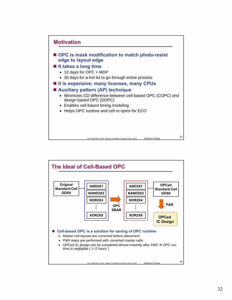
Motivation
OPC is mask modification to match photo-resist edge to layout edge It takes a long time• 12 days for OPC + MDP• 30 days for a hot lot to go through entire process
It is expensive: many licenses, many CPUsAuxiliary pattern (AP) technique• Minimizes CD difference between cell-based OPC (COPC) and
design-based OPC (DOPC)• Enables cell-based timing modeling • Helps OPC runtime and cell re-spins for ECO
64DAC-2006 DFM Tutorial: Nagaraj, Schoellkopf, Smayling, Wong, Kahng Andrew B. Kahng
The Ideal of Cell-Based OPC
Cell-based OPC is a solution for saving of OPC runtime• Master cell layouts are corrected before placement• P&R steps are performed with corrected master cells• OPCed IC design can be completed almost instantly after P&R OPC run
time is negligible ( 1~2 hours )
OriginalStandard-Cell
GDSII
AND2X1
NAND2X2
NOR2X4
XOR2X8
…
AND2X1
NAND2X2
NOR2X4
XOR2X8
… OPCSBAR
OPCedStandard-Cell
GDSII
OPCed IC Design
P&R
33
65DAC-2006 DFM Tutorial: Nagaraj, Schoellkopf, Smayling, Wong, Kahng Andrew B. Kahng
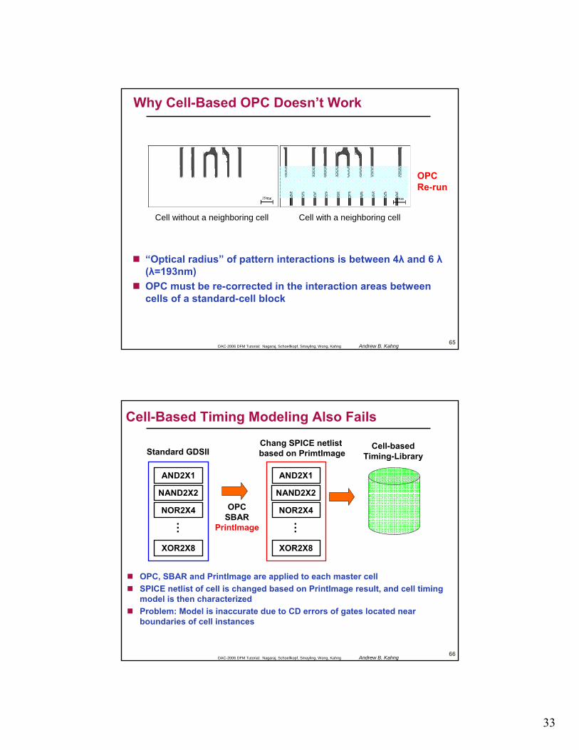
Why Cell-Based OPC Doesn’t Work
Cell without a neighboring cell Cell with a neighboring cell
OPCRe-run
“Optical radius” of pattern interactions is between 4λ and 6 λ(λ=193nm)OPC must be re-corrected in the interaction areas between cells of a standard-cell block
66DAC-2006 DFM Tutorial: Nagaraj, Schoellkopf, Smayling, Wong, Kahng Andrew B. Kahng
Cell-Based Timing Modeling Also Fails
OPC, SBAR and PrintImage are applied to each master cell SPICE netlist of cell is changed based on PrintImage result, and cell timing model is then characterizedProblem: Model is inaccurate due to CD errors of gates located near boundaries of cell instances
AND2X1
NAND2X2
NOR2X4
XOR2X8
…
AND2X1
NAND2X2
NOR2X4
XOR2X8
…
OPCSBAR
PrintImage
Standard GDSIIChang SPICE netlist based on PrimtImage
Cell-basedTiming-Library
34
67DAC-2006 DFM Tutorial: Nagaraj, Schoellkopf, Smayling, Wong, Kahng Andrew B. Kahng
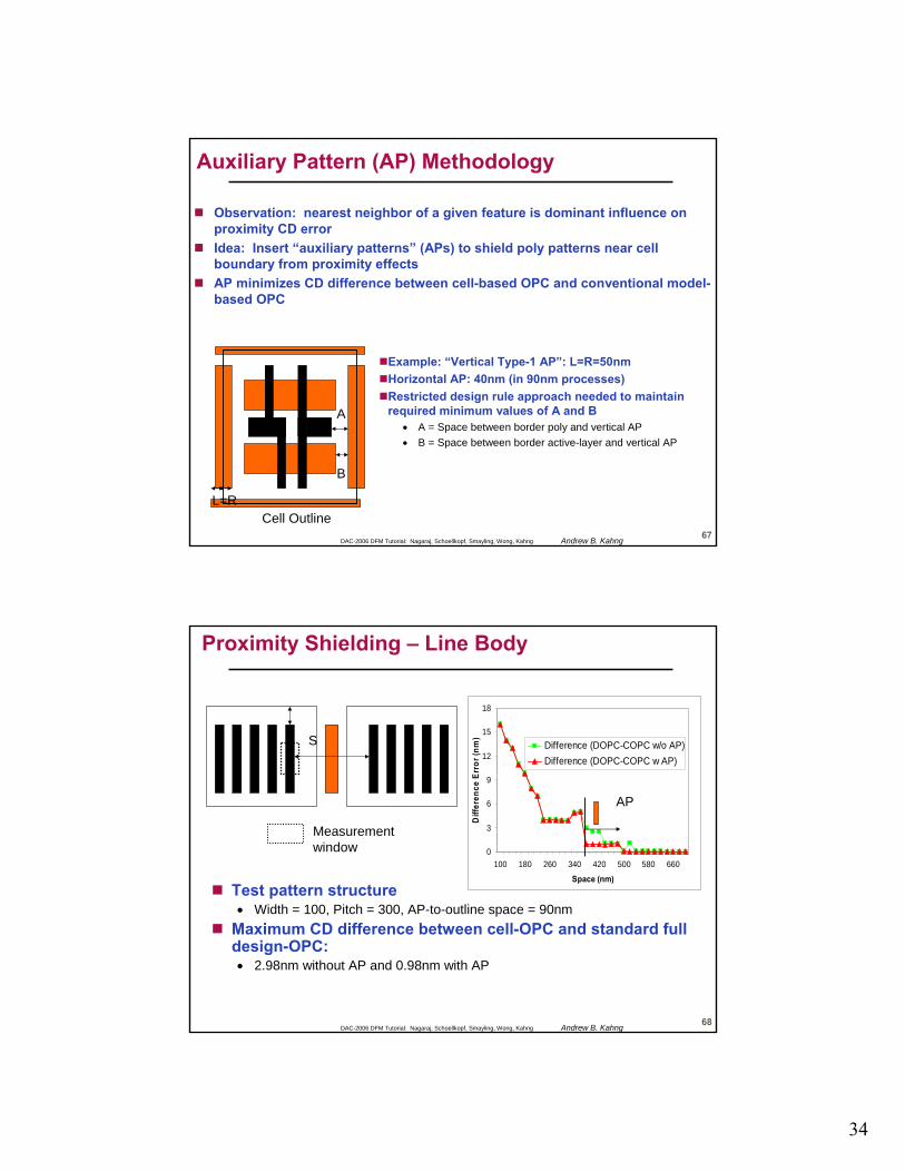
Auxiliary Pattern (AP) Methodology
Observation: nearest neighbor of a given feature is dominant influence on proximity CD errorIdea: Insert “auxiliary patterns” (APs) to shield poly patterns near cell boundary from proximity effectsAP minimizes CD difference between cell-based OPC and conventional model-based OPC
Example: “Vertical Type-1 AP”: L=R=50nmHorizontal AP: 40nm (in 90nm processes)Restricted design rule approach needed to maintain required minimum values of A and B
• A = Space between border poly and vertical AP • B = Space between border active-layer and vertical AP
A
B
L=RCell Outline
68DAC-2006 DFM Tutorial: Nagaraj, Schoellkopf, Smayling, Wong, Kahng Andrew B. Kahng
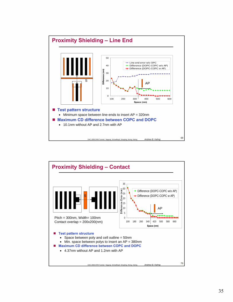
Proximity Shielding – Line Body
Test pattern structure• Width = 100, Pitch = 300, AP-to-outline space = 90nm
Maximum CD difference between cell-OPC and standard full design-OPC:• 2.98nm without AP and 0.98nm with AP
S
0
3
6
9
12
15
18
100 180 260 340 420 500 580 660
Space (nm)
Diff
eren
ce E
rror
(nm
)
Difference (DOPC-COPC w/o AP)Difference (DOPC-COPC w AP)
AP
Measurement window
35
69DAC-2006 DFM Tutorial: Nagaraj, Schoellkopf, Smayling, Wong, Kahng Andrew B. Kahng
Proximity Shielding – Line End
Test pattern structure• Minimum space between line-ends to insert AP = 320nm
Maximum CD difference between COPC and DOPC• 10.1nm without AP and 2.7nm with AP
S
0
10
20
30
40
50
100 200 300 400 500 600Space (nm)
Diff
eren
ce (n
m)
Line-end error w/o OPCDifference (DOPC-COPC w/o AP)Difference (DOPC-COPC w AP)
AP
70DAC-2006 DFM Tutorial: Nagaraj, Schoellkopf, Smayling, Wong, Kahng Andrew B. Kahng
Proximity Shielding – Contact
Pitch = 300nm, Width= 100nmContact overlap = 200x200(nm)
S
0
5
10
15
20
25
30
35
100 180 260 340 420 500 580 660
Space (nm)
Diff
eren
ce E
rror
(nm
)
Difference (DOPC-COPC w/o AP)Difference (DOPC-COPC w AP)
Test pattern structure• Space between poly and cell outline = 50nm• Min. space between polys to insert an AP = 380nm
Maximum CD difference between COPC and DOPC• 4.37nm without AP and 1.2nm with AP
AP
36
71DAC-2006 DFM Tutorial: Nagaraj, Schoellkopf, Smayling, Wong, Kahng Andrew B. Kahng
AP Flow Includes Placement Optimization
Standard Cell GDSII
OPCed Standard Cell
GDSII
AP Generation
SRAF Insertion
OPC
Placement
AP-CorrectPlacement
OPC GDSII
Post-Placement Optimization
Route
Idea: Use whitespace in the standard-cell block to maximize number of AP-augmented cell instances, and benefit from cell-based OPCRecall: *CORR technique in first part of this talk !
72DAC-2006 DFM Tutorial: Nagaraj, Schoellkopf, Smayling, Wong, Kahng Andrew B. Kahng
Result of AP InsertionAfter Post-Placement Opt (PO)
Placement Opt tries to put one placement site between cellsPost-placement optimization can lead to 100% cell-based OPC with utilizations of < 70%80+% of model-based OPC work is eliminated at 80% utilizations
Cell-Based OPC Becomes Practical !!!
4906207
000
7683380213001204702
W/O PO W PO90%80%70%60%50%
“ALU”
50541250
000
95737292302321131315
W/O PO W PO“AES”
UTIL %
37
73DAC-2006 DFM Tutorial: Nagaraj, Schoellkopf, Smayling, Wong, Kahng Andrew B. Kahng
Outline
Detailed Placement for Process Window EnhancementCMP Fill at 65nm and BelowAuxiliary Pattern Methodology for Cell-Based OPCCrosstalk Awareness in SSTAOther
DAC-2006 DFM Tutorial: Nagaraj, Schoellkopf, Smayling, Wong, Kahng Andrew B. Kahng
Increased variability in nanometer VLSI designs • Process:
• OPC Lgate• CMP thickness• Doping Vth
• Environment: • Supply voltage transistor performance• Temperature carrier mobility µ and Vth
These (PVT) variations result in circuit performance variation
p1
p2
PVT Parameter Distributions
d1
d2
Gate/net DelayDistribution
Variability
38
DAC-2006 DFM Tutorial: Nagaraj, Schoellkopf, Smayling, Wong, Kahng Andrew B. Kahng
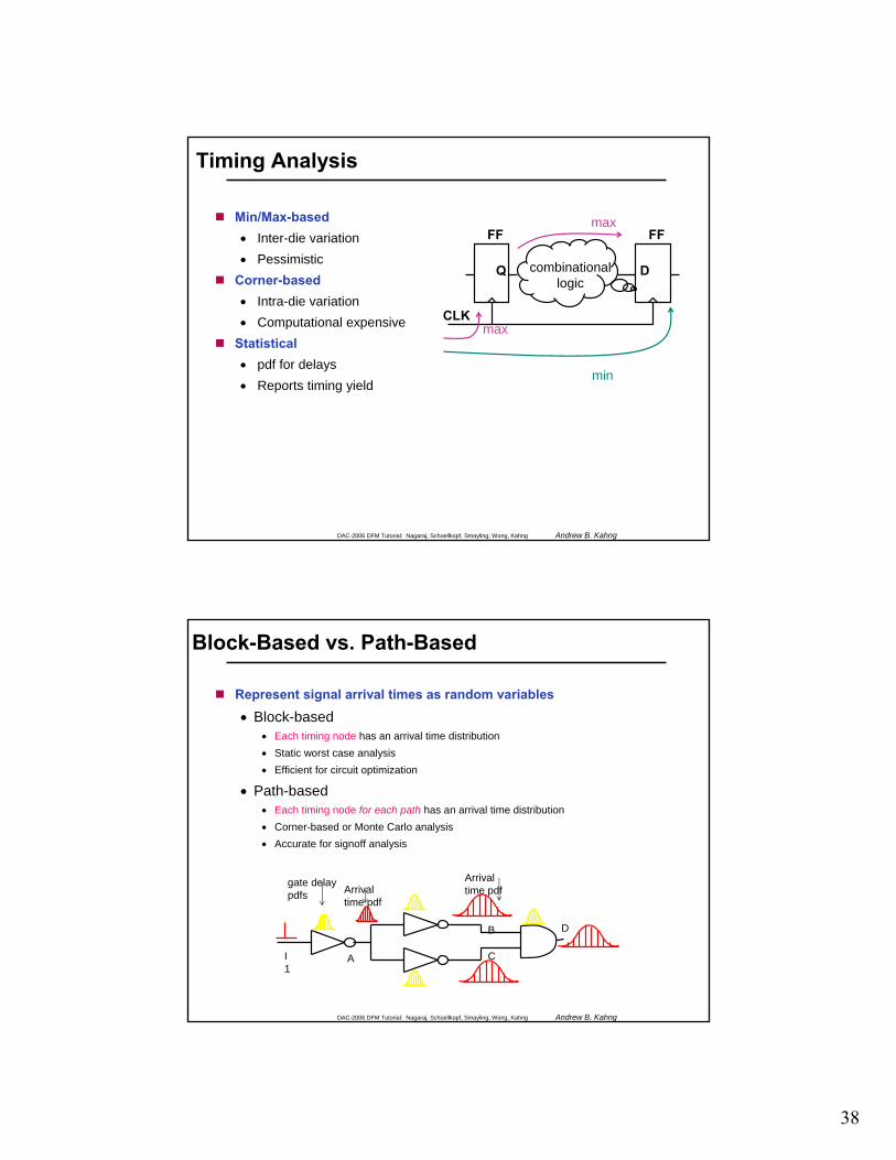
Min/Max-based• Inter-die variation• Pessimistic
Corner-based• Intra-die variation• Computational expensive
Statistical • pdf for delays • Reports timing yield
CLK
DQ combinationallogic
FF FF
max
max
min
Timing Analysis
DAC-2006 DFM Tutorial: Nagaraj, Schoellkopf, Smayling, Wong, Kahng Andrew B. Kahng
Represent signal arrival times as random variables
• Block-based • Each timing node has an arrival time distribution• Static worst case analysis • Efficient for circuit optimization
• Path-based • Each timing node for each path has an arrival time distribution• Corner-based or Monte Carlo analysis• Accurate for signoff analysis
B
CA
D
I1
gate delay pdfs
Arrival time pdfArrival
time pdf
Block-Based vs. Path-Based
39
77DAC-2006 DFM Tutorial: Nagaraj, Schoellkopf, Smayling, Wong, Kahng Andrew B. Kahng
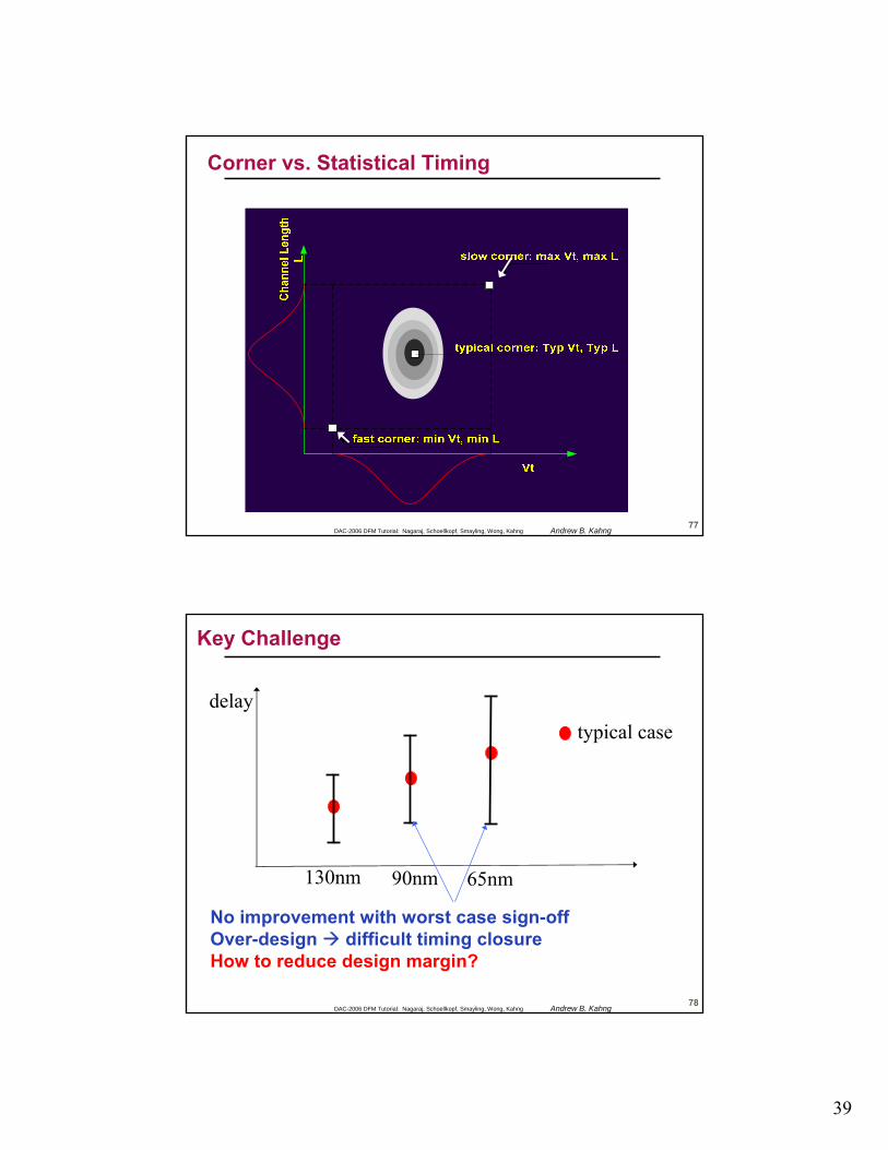
Corner vs. Statistical Timing
78DAC-2006 DFM Tutorial: Nagaraj, Schoellkopf, Smayling, Wong, Kahng Andrew B. Kahng
Key Challenge
No improvement with worst case sign-offOver-design difficult timing closure How to reduce design margin?
130nm 90nm 65nm
delaytypical case
40
79DAC-2006 DFM Tutorial: Nagaraj, Schoellkopf, Smayling, Wong, Kahng Andrew B. Kahng
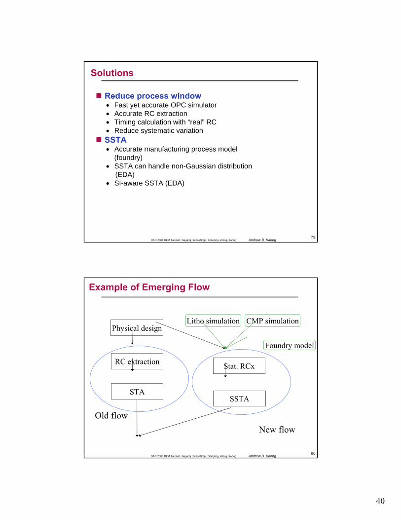
Solutions
Reduce process window• Fast yet accurate OPC simulator• Accurate RC extraction• Timing calculation with “real” RC• Reduce systematic variationSSTA• Accurate manufacturing process model
(foundry) • SSTA can handle non-Gaussian distribution
(EDA) • SI-aware SSTA (EDA)
80DAC-2006 DFM Tutorial: Nagaraj, Schoellkopf, Smayling, Wong, Kahng Andrew B. Kahng
Example of Emerging Flow
Physical design
RC extraction
STA
Stat. RCx
SSTA
Old flowNew flow
Litho simulation CMP simulation
Foundry model
41
DAC-2006 DFM Tutorial: Nagaraj, Schoellkopf, Smayling, Wong, Kahng Andrew B. Kahng
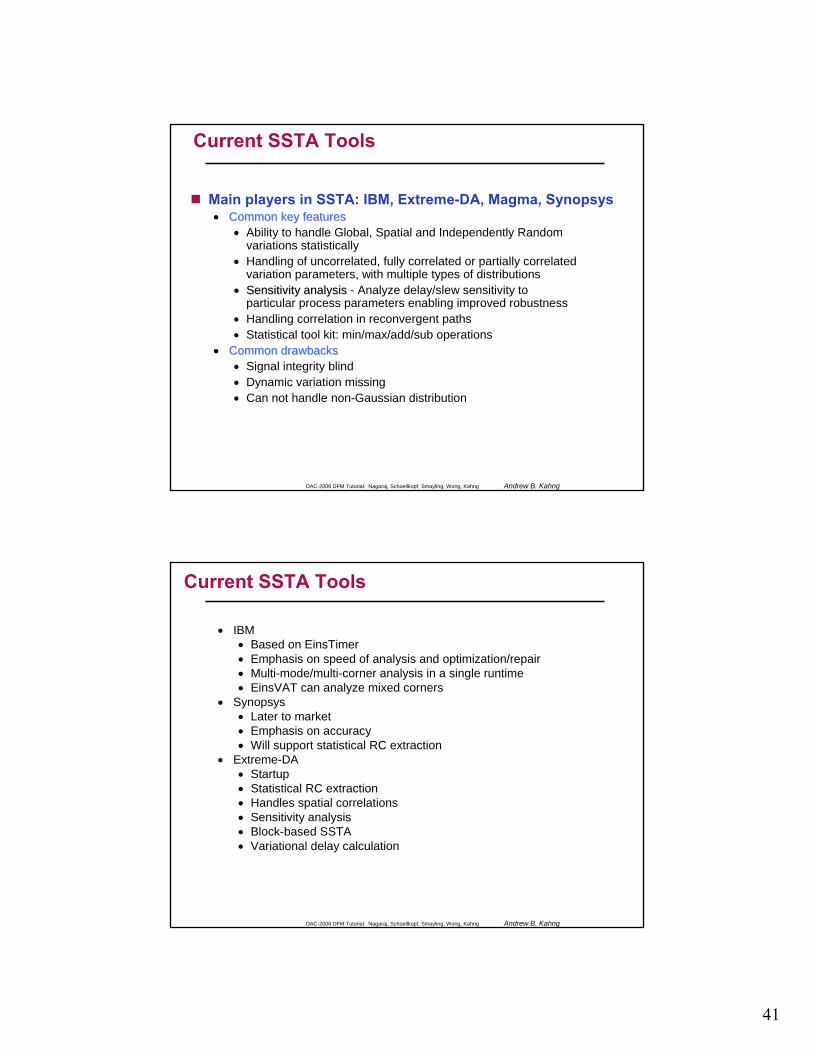
Current SSTA Tools
Main players in SSTA: IBM, Extreme-DA, Magma, Synopsys•• Common key featuresCommon key features
• Ability to handle Global, Spatial and Independently Random variations statistically
• Handling of uncorrelated, fully correlated or partially correlated variation parameters, with multiple types of distributions
•• Sensitivity analysisSensitivity analysis - Analyze delay/slew sensitivity to particular process parameters enabling improved robustness
• Handling correlation in reconvergent paths• Statistical tool kit: min/max/add/sub operations
•• Common drawbacksCommon drawbacks• Signal integrity blind• Dynamic variation missing• Can not handle non-Gaussian distribution
DAC-2006 DFM Tutorial: Nagaraj, Schoellkopf, Smayling, Wong, Kahng Andrew B. Kahng
Current SSTA Tools
• IBM• Based on EinsTimer• Emphasis on speed of analysis and optimization/repair• Multi-mode/multi-corner analysis in a single runtime• EinsVAT can analyze mixed corners
• Synopsys• Later to market• Emphasis on accuracy• Will support statistical RC extraction
• Extreme-DA• Startup• Statistical RC extraction• Handles spatial correlations• Sensitivity analysis• Block-based SSTA• Variational delay calculation
42
DAC-2006 DFM Tutorial: Nagaraj, Schoellkopf, Smayling, Wong, Kahng Andrew B. Kahng
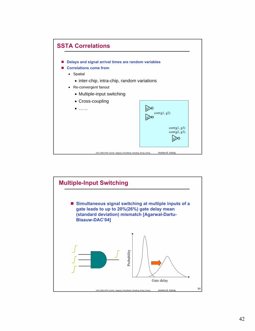
Delays and signal arrival times are random variablesCorrelations come from• Spatial
• inter-chip, intra-chip, random variations• Re-convergent fanout
• Multiple-input switching• Cross-coupling • ……
corr(g1, g2)g1
g2
g3
corr(g1, g3)corr(g2, g3)
SSTA Correlations
84DAC-2006 DFM Tutorial: Nagaraj, Schoellkopf, Smayling, Wong, Kahng Andrew B. Kahng
Multiple-Input Switching
Simultaneous signal switching at multiple inputs of a gate leads to up to 20%(26%) gate delay mean (standard deviation) mismatch [Agarwal-Dartu-Blaauw-DAC’04]
Gate delay
Prob
abili
ty
43
85DAC-2006 DFM Tutorial: Nagaraj, Schoellkopf, Smayling, Wong, Kahng Andrew B. Kahng
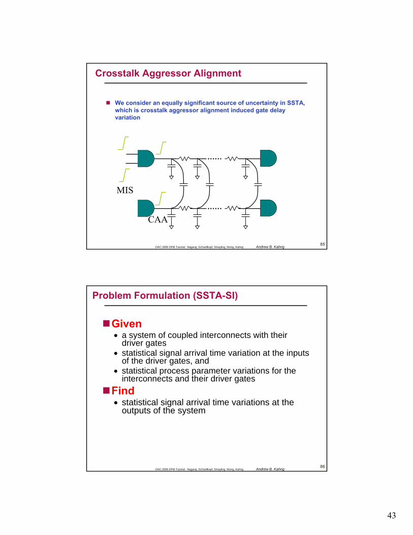
Crosstalk Aggressor Alignment
We consider an equally significant source of uncertainty in SSTA, which is crosstalk aggressor alignment induced gate delay variation
MIS
CAA
86DAC-2006 DFM Tutorial: Nagaraj, Schoellkopf, Smayling, Wong, Kahng Andrew B. Kahng
Problem Formulation (SSTA-SI)
Given• a system of coupled interconnects with their
driver gates• statistical signal arrival time variation at the inputs
of the driver gates, and • statistical process parameter variations for the
interconnects and their driver gatesFind• statistical signal arrival time variations at the
outputs of the system
44
87DAC-2006 DFM Tutorial: Nagaraj, Schoellkopf, Smayling, Wong, Kahng Andrew B. Kahng
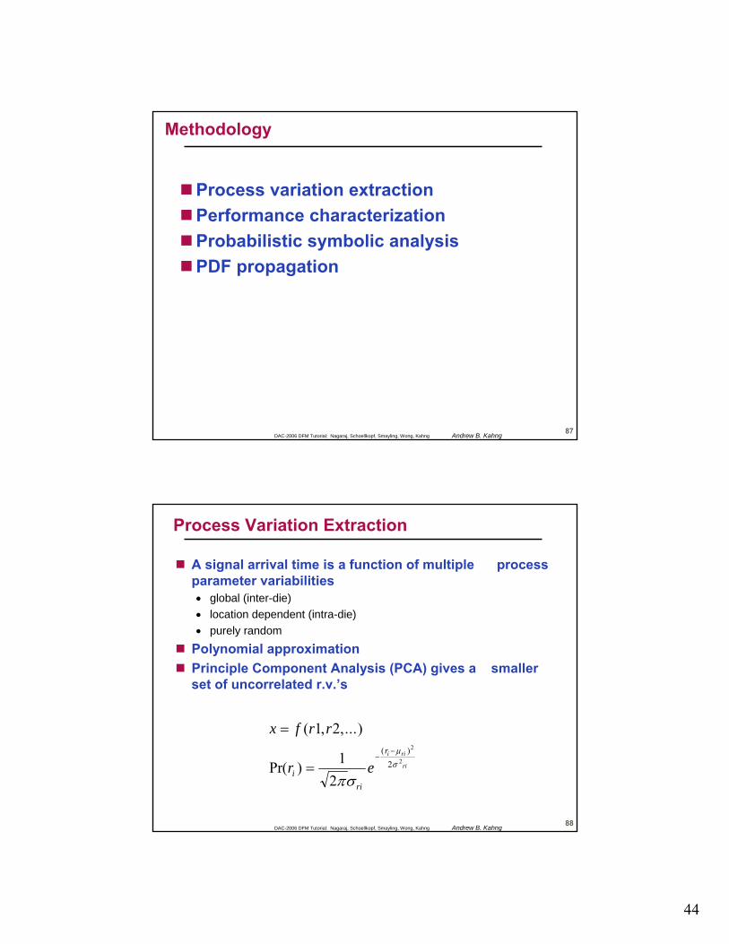
Methodology
Process variation extraction Performance characterizationProbabilistic symbolic analysisPDF propagation
88DAC-2006 DFM Tutorial: Nagaraj, Schoellkopf, Smayling, Wong, Kahng Andrew B. Kahng
Process Variation Extraction
A signal arrival time is a function of multiple process parameter variabilities• global (inter-die)• location dependent (intra-die)• purely random
Polynomial approximationPrinciple Component Analysis (PCA) gives a smaller set of uncorrelated r.v.’s
x f r r
r eiri
ri ri
ri
=
=−
−
( , ,...)
Pr( )( )
1 2
12
2
22
πσ
µσ
45
89DAC-2006 DFM Tutorial: Nagaraj, Schoellkopf, Smayling, Wong, Kahng Andrew B. Kahng
Performance Characterization
Delay calculation for sampled crosstalk alignmentsLeast mean square regression for piecewise quadratic polynomial approximation
τ =
<+ + < <
< <+ + < <
<
⎧
⎨
⎪⎪⎪
⎩
⎪⎪⎪
d x ta a x a x t x t
d t x tb b x b x t x t
d t x
2 0
0 1 22
0 1
0 1 2
0 1 22
2 3
1 3
'' ' '
'' ' '
'
90DAC-2006 DFM Tutorial: Nagaraj, Schoellkopf, Smayling, Wong, Kahng Andrew B. Kahng
PDF Propagation
Given• Joint probabilistic density function of k
random variables x• A piecewise polynomial function y = f(x)
Find• Probabilistic density function of y
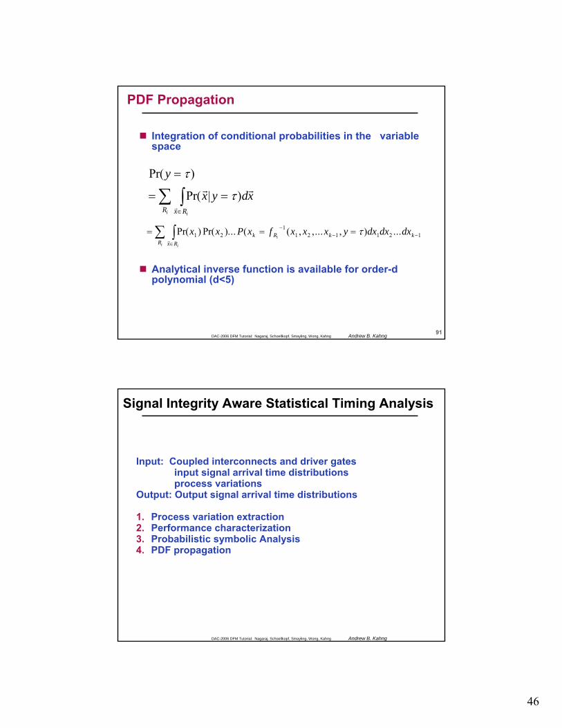
46
91DAC-2006 DFM Tutorial: Nagaraj, Schoellkopf, Smayling, Wong, Kahng Andrew B. Kahng
Integration of conditional probabilities in the variable space
Analytical inverse function is available for order-d polynomial (d<5)
PDF Propagation
Pr( )
Pr( | )
y
x y dxx RR ii
=
= =∈∫∑τ
τr r
r
= = =−− −
∈∫∑ Pr( ) Pr( )... ( ( , ,... , ) ...x x P x f x x x y dx dx dxk R k k
x RRi
ii
1 21
1 2 1 1 2 1τr
DAC-2006 DFM Tutorial: Nagaraj, Schoellkopf, Smayling, Wong, Kahng Andrew B. Kahng
Input: Coupled interconnects and driver gatesinput signal arrival time distributions process variations
Output: Output signal arrival time distributions
1. Process variation extraction2. Performance characterization3. Probabilistic symbolic Analysis4. PDF propagation
Signal Integrity Aware Statistical Timing Analysis
47
DAC-2006 DFM Tutorial: Nagaraj, Schoellkopf, Smayling, Wong, Kahng Andrew B. Kahng
STA-SI goes through an iteration of timing window refinement for reduced pessimism of worst case analysis
SSTA-SI goes through an iteration of signal arrival time pdf refinement with reduced deviations
Implementation
DAC-2006 DFM Tutorial: Nagaraj, Schoellkopf, Smayling, Wong, Kahng Andrew B. Kahng
Performance characterization for N sampled crosstalk alignments takes O(N) time, where N = min(t3-t0, 6 σ of crosstalk alignment) / time_stepRegression takes O(N) timeComputing output signal arrival time distribution takes constant time, e.g., updating in an iterative SSTA
Runtime Analysis
48
DAC-2006 DFM Tutorial: Nagaraj, Schoellkopf, Smayling, Wong, Kahng Andrew B. Kahng
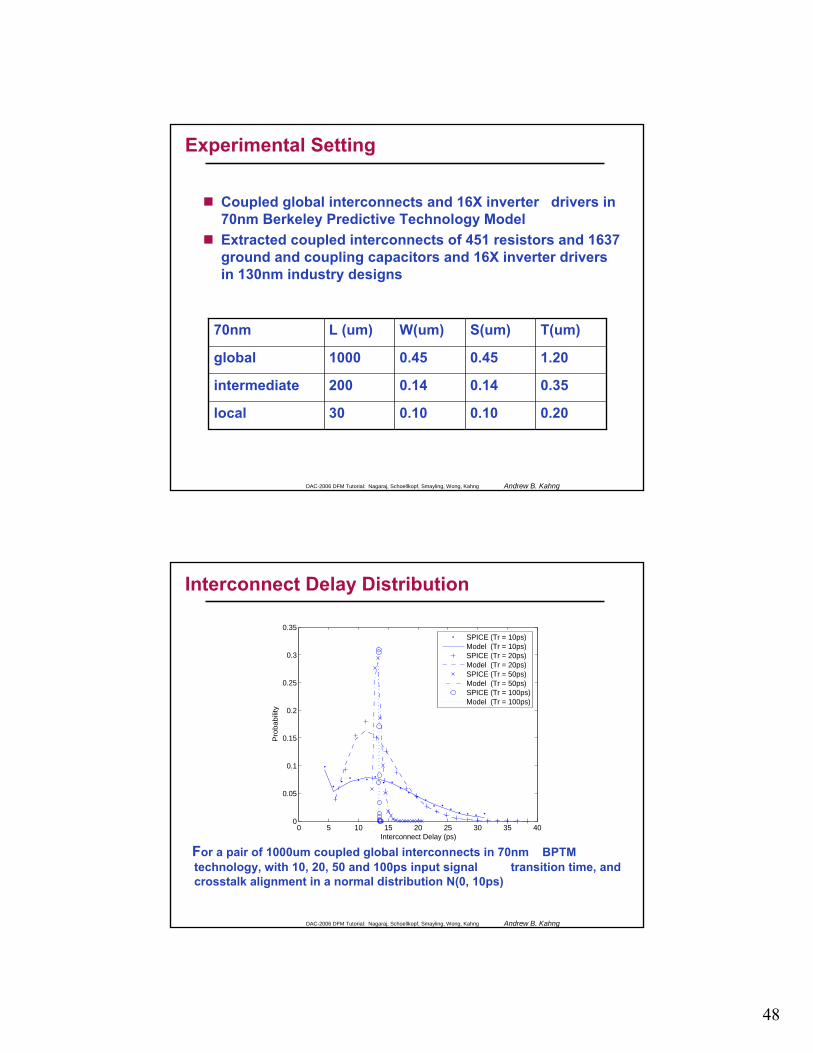
Coupled global interconnects and 16X inverter drivers in 70nm Berkeley Predictive Technology ModelExtracted coupled interconnects of 451 resistors and 1637 ground and coupling capacitors and 16X inverter drivers in 130nm industry designs
0.200.100.1030local
0.350.140.14200intermediate
1.200.450.451000global
T(um)S(um)W(um)L (um)70nm
Experimental Setting
DAC-2006 DFM Tutorial: Nagaraj, Schoellkopf, Smayling, Wong, Kahng Andrew B. Kahng
0 5 10 15 20 25 30 35 400
0.05
0.1
0.15
0.2
0.25
0.3
0.35
Interconnect Delay (ps)
Pro
babi
lity
SPICE (Tr = 10ps)Model (Tr = 10ps)SPICE (Tr = 20ps)Model (Tr = 20ps)SPICE (Tr = 50ps)Model (Tr = 50ps)SPICE (Tr = 100ps)Model (Tr = 100ps)
For a pair of 1000um coupled global interconnects in 70nm BPTMtechnology, with 10, 20, 50 and 100ps input signal transition time, and crosstalk alignment in a normal distribution N(0, 10ps)
Interconnect Delay Distribution
49
DAC-2006 DFM Tutorial: Nagaraj, Schoellkopf, Smayling, Wong, Kahng Andrew B. Kahng
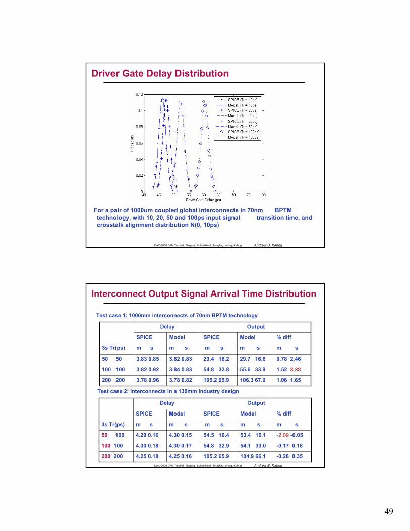
For a pair of 1000um coupled global interconnects in 70nm BPTM technology, with 10, 20, 50 and 100ps input signal transition time, and crosstalk alignment distribution N(0, 10ps)
Driver Gate Delay Distribution
DAC-2006 DFM Tutorial: Nagaraj, Schoellkopf, Smayling, Wong, Kahng Andrew B. Kahng
% diff ModelSPICEModelSPICE
m sm sm sm sm s3s Tr(ps)
1.06 1.65106.3 67.0105.2 65.93.78 0.823.78 0.96200 200
1.52 3.3855.6 33.954.8 32.83.84 0.833.82 0.92100 100
0.78 2.4629.7 16.629.4 16.23.82 0.833.83 0.8550 50
Output Delay
Test case 2: interconnects in a 130mm industry design
Test case 1: 1000mm interconnects of 70nm BPTM technology
% diff ModelSPICEModelSPICE
m sm sm sm sm s3s Tr(ps)
-0.28 0.35104.9 66.1105.2 65.94.25 0.164.25 0.18200 200
-0.17 0.1854.1 33.054.8 32.94.30 0.174.30 0.18100 100
-2.09 -0.0553.4 16.154.5 16.44.30 0.154.29 0.1650 100
Output Delay
Interconnect Output Signal Arrival Time Distribution
50
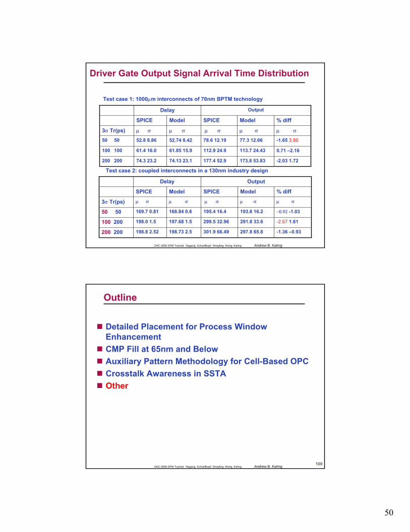
DAC-2006 DFM Tutorial: Nagaraj, Schoellkopf, Smayling, Wong, Kahng Andrew B. Kahng
% diff ModelSPICEModelSPICE
-2.03 1.72173.8 53.83177.4 52.974.13 23.174.3 23.2200 200
0.71 –2.16113.7 24.43112.9 24.961.85 15.961.4 16.0100 100
-1.65 3.8677.3 12.6678.6 12.1952.74 8.4252.8 8.8650 50
µ σµ σµ σµ σµ σ3σ Tr(ps)
Output Delay
Test case 2: coupled interconnects in a 130nm industry design
Test case 1: 1000µm interconnects of 70nm BPTM technology
% diff ModelSPICEModelSPICE
-1.36 –0.93297.8 65.8301.9 66.49198.73 2.5198.8 2.52200 200
-2.57 1.61291.8 33.6299.5 32.96197.68 1.5198.0 1.5100 200
−0.92 -1.03193.6 16.2195.4 16.4168.84 0.8169.7 0.8150 50
µ σµ σµ σµ σµ σ3σ Tr(ps)
Output Delay
Driver Gate Output Signal Arrival Time Distribution
100DAC-2006 DFM Tutorial: Nagaraj, Schoellkopf, Smayling, Wong, Kahng Andrew B. Kahng
Outline
Detailed Placement for Process Window EnhancementCMP Fill at 65nm and BelowAuxiliary Pattern Methodology for Cell-Based OPCCrosstalk Awareness in SSTAOther
51
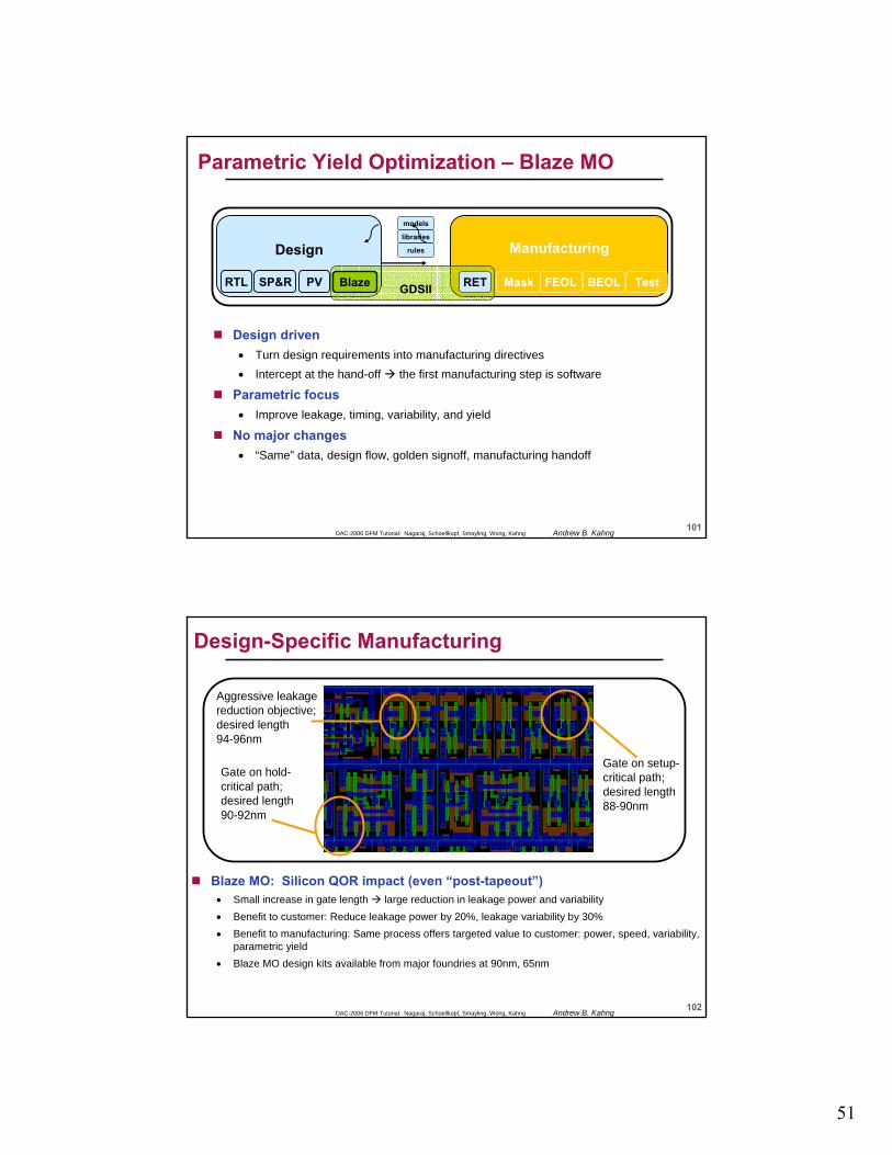
101DAC-2006 DFM Tutorial: Nagaraj, Schoellkopf, Smayling, Wong, Kahng Andrew B. Kahng
Design driven• Turn design requirements into manufacturing directives• Intercept at the hand-off the first manufacturing step is software
Parametric focus• Improve leakage, timing, variability, and yield
No major changes• “Same” data, design flow, golden signoff, manufacturing handoff
Parametric Yield Optimization – Blaze MO
Design
RTL SP&R PV
models
libraries
rules Manufacturing
Mask FEOL BEOL TestGDSIIBlaze RET
102DAC-2006 DFM Tutorial: Nagaraj, Schoellkopf, Smayling, Wong, Kahng Andrew B. Kahng
Blaze MO: Silicon QOR impact (even “post-tapeout”)• Small increase in gate length large reduction in leakage power and variability• Benefit to customer: Reduce leakage power by 20%, leakage variability by 30%• Benefit to manufacturing: Same process offers targeted value to customer: power, speed, variability,
parametric yield• Blaze MO design kits available from major foundries at 90nm, 65nm
*Patent Pending
Gate on hold-critical path; desired length 90-92nm
Gate on setup-critical path; desired length 88-90nm
Aggressive leakage reduction objective; desired length 94-96nm
Design-Specific Manufacturing
52
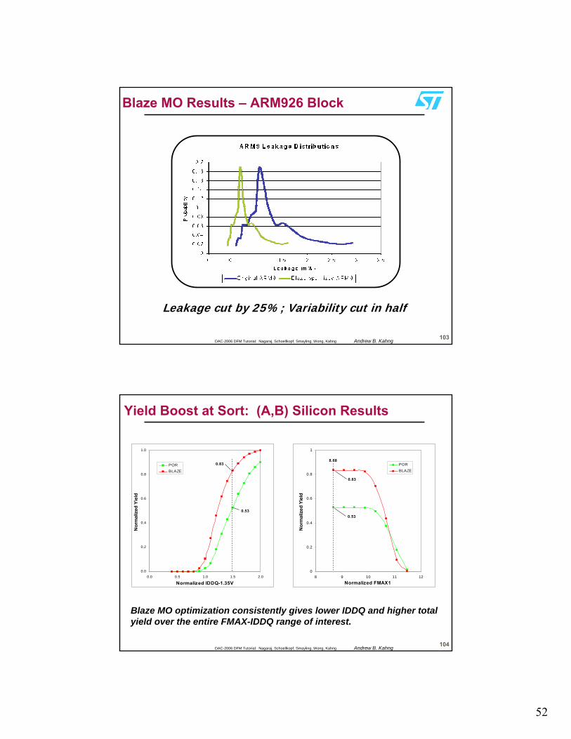
103DAC-2006 DFM Tutorial: Nagaraj, Schoellkopf, Smayling, Wong, Kahng Andrew B. Kahng
Leakage cut by 25%; Variability cut in half
Blaze MO Results – ARM926 Block
104DAC-2006 DFM Tutorial: Nagaraj, Schoellkopf, Smayling, Wong, Kahng Andrew B. Kahng
Yield Boost at Sort: (A,B) Silicon Results
Blaze MO optimization consistently gives lower IDDQ and higher total yield over the entire FMAX-IDDQ range of interest.
0.0
0.2
0.4
0.6
0.8
1.0
0.0 0.5 1.0 1.5 2.0
Normalized IDDQ-1.35V
Nor
mal
ized
Yie
ld
PORBLAZE
0.83
0.53
0
0.2
0.4
0.6
0.8
1
8 9 10 11 12Normalized FMAX1
Nor
mal
ized
Yie
ld
PORBLAZE
8.68
0.83
0.53
53
105DAC-2006 DFM Tutorial: Nagaraj, Schoellkopf, Smayling, Wong, Kahng Andrew B. Kahng
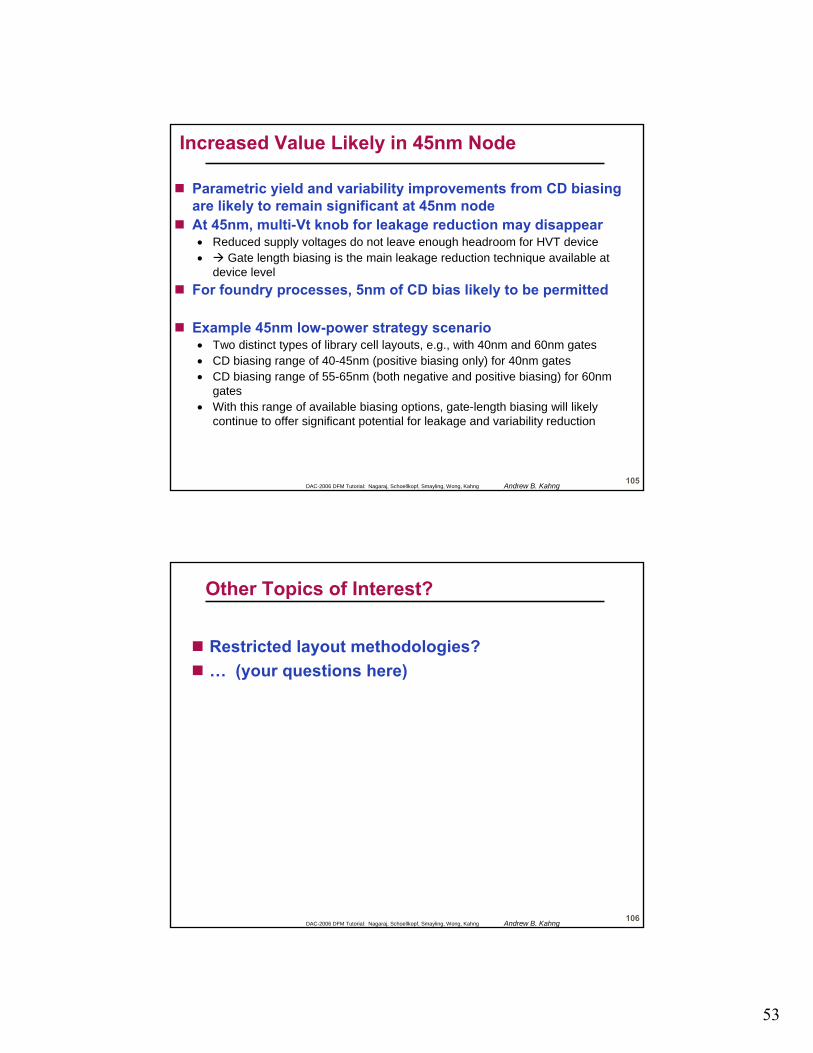
Increased Value Likely in 45nm Node
Parametric yield and variability improvements from CD biasing are likely to remain significant at 45nm nodeAt 45nm, multi-Vt knob for leakage reduction may disappear• Reduced supply voltages do not leave enough headroom for HVT device• Gate length biasing is the main leakage reduction technique available at
device levelFor foundry processes, 5nm of CD bias likely to be permitted
Example 45nm low-power strategy scenario• Two distinct types of library cell layouts, e.g., with 40nm and 60nm gates• CD biasing range of 40-45nm (positive biasing only) for 40nm gates• CD biasing range of 55-65nm (both negative and positive biasing) for 60nm
gates• With this range of available biasing options, gate-length biasing will likely
continue to offer significant potential for leakage and variability reduction
106DAC-2006 DFM Tutorial: Nagaraj, Schoellkopf, Smayling, Wong, Kahng Andrew B. Kahng
Other Topics of Interest?
Restricted layout methodologies?… (your questions here)


![Parallel VLSI CAD Algorithmszhuofeng/EE5900Spring2012... · Parallel VLSI CAD Algorithms Lecture 1 Introduction ... Various IEEE journal and conference papers: IEEE[1] Various IEEE](https://img.pdfslide.us/doc/110x75/5e88f1299475ec1f5a74fb96/parallel-vlsi-cad-algorithms-zhuofengee5900spring2012-parallel-vlsi-cad-algorithms.jpg)