Embed Size (px)
DESCRIPTION
PART 2
Citation preview
2
A New Approach to Biasing Design of Analog Circuits
Reza Hashemian Northern Illinois University
United States
1. Introduction A new approach for biasing analog circuits is introduced in this chapter. This approach is an attempt to address some of the biasing complexities that exist today in biasing large analog circuits. There are three steps involved in this methodology. First, in circuit analysis, the methodology separates nonlinear components (transistors), particularly drivers, from the rest of the circuit. Second, it uses local biasing introduced in the previous chapter to bias the transistors individually and to the specs provided for the design. Finally, the method presents a new way to change the local biasing into normal (global) circuit biasing with choices of DC supplies at right locations in the circuit. It is the last step that will be our main topic of discussion in this chapter. Here we see how we can remove all sources related to the local biasing and replace them with normal circuit supplies without altering the design specifications. These circuit supplies can be voltage sources, current sources or mirrors. In case the supplies are already specified and in place, this method can still maintain the design specs by re-evaluating some of the power-conducting components in the circuit. Power-conducting components are those circuit components, such as resistors, that conduct DC power (current) from the power supplies to the circuit drivers (transistors), for biasing purposes. Limitations in local Biasing - We fully discussed local biasing, its properties and applications in the previous chapter. Despite all the advantages that local biasing offers one problem still remains unresolved and that is: how to deal with so many DC sources generated due to local biasing, known as distributed supplies? To see the problem, just take a single bipolar transistor: it normally needs four (voltage and current) sources to get locally biased; however, with coupling capacitors used this number reduces to two current sources and two capacitors (taking care of the voltage drops). Similarly, we may need to use four sources to locally bias a MOS transistor. Again, with coupling capacitors this number can get as low as one source-drain current source. The problem, however, is that for the gate, and possibly the substrate, the coupling capacitors need to have charging paths (a resistive path to a DC supply). One way to handle the case and bring the number of DC supplies down to a minimum of one or two is to use source transformation and replacement techniques, such as voltage dividers, Δ-Y transformation, and current sources/mirrors. Nevertheless, the sheer number of such sources in a fairly complex circuit can get so high that unless we find a shortcut to the final solution the validity of local biasing as an effective methodology is undermined.

Advances in Analog Circuits
16
A new strategy - We are introducing a different strategy for biasing analog circuits in this chapter. The core of this strategy lies on the fact that in an analog circuit design environment we only need to anchor down certain critical biasing specs and not all. By critical biasing specs we mean those operating conditions that are essential in achieving the design criteria, such as gains, undistorted output signals or power consumption. Other design criteria usually adhere to these critical specs and adapt to the situation fairly well enforced by the critical specs. The fact that DC supplies are present in a circuit only to bias the nonlinear components reveals the fact that for each biasing (critical) spec we need to provide a path to a DC power supply, controlled by the spec. With this in mind, the proposed strategy makes a one-to-one correspondence between the circuit biasing requirements (specs) and those DC (voltage or current) supplies needed to support these requirements. Hence, we need at least as many path to DC power supplies as we have biasing specs in a circuit. Consequently, the first task in this strategy is to pair each biasing spec with a biasing supply (voltage, current or a power-conducting component). Second, the method must be capable of replacing “distributed supplies” -- if a local biasing strategy is already in use -- with normal circuit supplies, such as VCC and VDD. The idea here is to keep the main properties of local biasing – translated into the critical biasing specs -- while removing local biasing sources to be replaced with the normal biasing supplies. The main advantages in employing this strategy are: i) to pin down the operating conditions for the critical transistors while replacing the local biasing sources with a much fewer designated DC supplies, ii) to minimize design efforts to fulfill only critical specs, hence speeding up the process, and iii) the possibility to perform biasing entirely linearly. The last point is particularly important and makes biasing almost a one-step process. This chapter introduces two new circuit elements, fixator and norator, that are the center pieces in our biasing design strategy. Fixators and norators come in pairs as effective tools to perform a targeted biasing. It is shown that these pairs are very instrumental in matching biasing critical specs with DC power resources. The method simply associates a designated supply source (or a power-conducting component) with an arbitrary biasing spec. Fixator-norator pairs cause local biasing sources (distributed supplies) to be entirely replaced with normal circuit supplies designated by the designer. It is shown that the pair, when used properly and in combination, will adhere to Kirchhoff laws as well. Important properties of fixator-norator pairs are introduced in this chapter, and the relationships between a fixator-norator pair and other circuit components (such as resistors, voltage sources, and current sources) are discussed. Rules and regulations corresponding to the use of fixator-norator pairs in a circuit are investigated. Being special circuit components, fixators and norators must be used so that KVL and KCL are not violated in a circuit. However, it is important to note that the use of fixator-norator pairs is only temporary in this methodology; i.e., the pairs are removed as soon as the final circuit biasing is established and the DC power is provided for the circuit. This is important in a sense that ideal controlled sources, with very high gains, can be used to mimic fixator-norator pairs without any restrictions. Because fixators can model fixed-biased ports, these devices can also model nonlinear components for specified biasing situations. These nonlinear components can be p-n junction diodes (as single port devices), bipolar transistors (as two port devices), and MOS transistors (as three port devices). An algorithm that explains the biasing design procedure of analog circuits is also introduced in this chapter. This algorithm classifies circuit design procedure into two areas: the performance (AC) design and the biasing design. The performance design (gain, bandwidth,
A New Approach to Biasing Design of Analog Circuits
17
SNR, power, distortion, and so on) is done first. Here is where the circuit topology and the major circuit components are determined to achieve the design goals. In the performance design the circuit is treated entirely linear, where the transistors are replaced with their linear models at specifies operating points. Upon finishing the performance design the circuit biasing design begins by providing a set of critical biasing specs. It is in this stage that the linear models of the transistors (used in the performance design) are replaced with the fixator models. Next, the designer needs to accommodate for the norators that must pair with the fixators. He/she has variety of choices to place the pairing norators in the circuit; having in mind that they are place holders for the power supplies, current sources/mirrors, or power-conducting components. When finished, the circuit is ready for simulation, while still linear. The results from the DC solution contain the voltage and current values for each norator; where, each in turn can be replaced with an appropriate component. This completes the DC design procedure.
1.1 Circuit biasing Biasing is a major step in designing analog circuits [1 – 3]. In large and complex circuits biasing has always been a great challenge for designers. The challenge is normally in two areas. First, to get the number of iterations minimized and make the convergence possible and fast; second, to move to the right regions of operations for active components (transistors) so that acceptable performance is attained and the output signals are far from being distorted or clipped during the AC operation. Both problems grow in complexity as the number of transistors increases, design requirements become tighter, or more efficient designs are in demand. One difficulty in the traditional approach appears to be the lack of separation between linear and nonlinear components, as well as between the nonlinear components themselves during the biasing process. Typical biasing techniques deal with the entire circuit as a whole with no classification or circuit partitioning; hence, the complexity quickly increases as the circuit grows. In case of analog ICs, where almost all circuit components are nonlinear, distinction between linear and nonlinear components becomes meaningless. Instead we can categorize components into two categories: i) drivers, and ii) supporting components. In conventional methods used for the analysis and simulation of analog circuits all nonlinear components, regardless of their categories and functionalities, are included in a global biasing (DC) analysis. Whereas in more advanced methods we can distinguish between the drivers and those supporting components, such as current sources/sinks, current mirrors, and active loads [4 - 6]. Drivers typically reside along the signal path directly shaping the output waveforms. They are strongly influencing the design specifications, and are more sensitive to signal conditionings. Consequently, drivers must be biased with more care and precision compared to the supporting components in a circuit.
2. Nullators, fixators and norators We first need to define terms that are used in this chapter. In addition, all our discussions here apply to DC power unless stated otherwise.
2.1 Port parameter fixing The methodology introduced here is based on assigning specific operating points to nonlinear ports (in diodes and transistors) during the biasing design of an analog circuit.
Advances in Analog Circuits
18
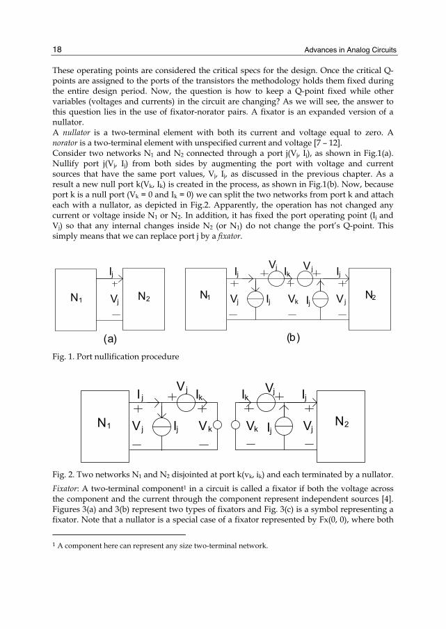
These operating points are considered the critical specs for the design. Once the critical Q-points are assigned to the ports of the transistors the methodology holds them fixed during the entire design period. Now, the question is how to keep a Q-point fixed while other variables (voltages and currents) in the circuit are changing? As we will see, the answer to this question lies in the use of fixator-norator pairs. A fixator is an expanded version of a nullator. A nullator is a two-terminal element with both its current and voltage equal to zero. A norator is a two-terminal element with unspecified current and voltage [7 – 12]. Consider two networks N1 and N2 connected through a port j(Vj, Ij), as shown in Fig.1(a). Nullify port j(Vj, Ij) from both sides by augmenting the port with voltage and current sources that have the same port values, Vj, Ij, as discussed in the previous chapter. As a result a new null port k(Vk, Ik) is created in the process, as shown in Fig.1(b). Now, because port k is a null port (Vk = 0 and Ik = 0) we can split the two networks from port k and attach each with a nullator, as depicted in Fig.2. Apparently, the operation has not changed any current or voltage inside N1 or N2. In addition, it has fixed the port operating point (Ij and Vj) so that any internal changes inside N2 (or N1) do not change the port’s Q-point. This simply means that we can replace port j by a fixator.
N1 N2
Ij
Vj
(a) (b)
N2
Ij
VjIj
VjIk
VkN1 Ij
VjIj
Vj
Fig. 1. Port nullification procedure
N2
Ij
VjIj
VjIk
VkN1 Ij
VjI j
Vj
Ik
Vk
Fig. 2. Two networks N1 and N2 disjointed at port k(vk, ik) and each terminated by a nullator.
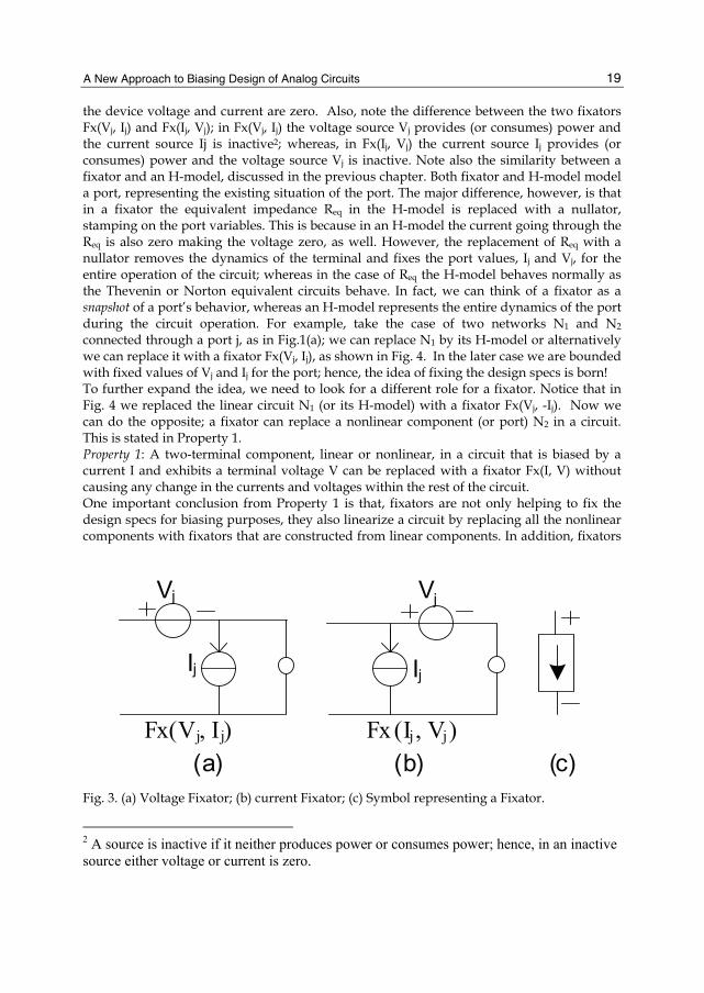
Fixator: A two-terminal component1 in a circuit is called a fixator if both the voltage across the component and the current through the component represent independent sources [4]. Figures 3(a) and 3(b) represent two types of fixators and Fig. 3(c) is a symbol representing a fixator. Note that a nullator is a special case of a fixator represented by Fx(0, 0), where both
1 A component here can represent any size two-terminal network.
A New Approach to Biasing Design of Analog Circuits
19
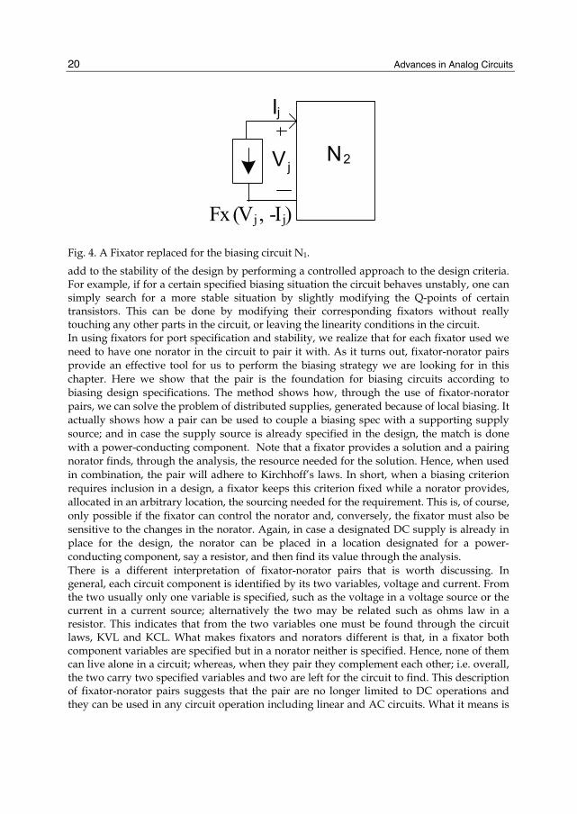
the device voltage and current are zero. Also, note the difference between the two fixators Fx(Vj, Ij) and Fx(Ij, Vj); in Fx(Vj, Ij) the voltage source Vj provides (or consumes) power and the current source Ij is inactive2; whereas, in Fx(Ij, Vj) the current source Ij provides (or consumes) power and the voltage source Vj is inactive. Note also the similarity between a fixator and an H-model, discussed in the previous chapter. Both fixator and H-model model a port, representing the existing situation of the port. The major difference, however, is that in a fixator the equivalent impedance Req in the H-model is replaced with a nullator, stamping on the port variables. This is because in an H-model the current going through the Req is also zero making the voltage zero, as well. However, the replacement of Req with a nullator removes the dynamics of the terminal and fixes the port values, Ij and Vj, for the entire operation of the circuit; whereas in the case of Req the H-model behaves normally as the Thevenin or Norton equivalent circuits behave. In fact, we can think of a fixator as a snapshot of a port’s behavior, whereas an H-model represents the entire dynamics of the port during the circuit operation. For example, take the case of two networks N1 and N2 connected through a port j, as in Fig.1(a); we can replace N1 by its H-model or alternatively we can replace it with a fixator Fx(Vj, Ij), as shown in Fig. 4. In the later case we are bounded with fixed values of Vj and Ij for the port; hence, the idea of fixing the design specs is born! To further expand the idea, we need to look for a different role for a fixator. Notice that in Fig. 4 we replaced the linear circuit N1 (or its H-model) with a fixator Fx(Vj, -Ij). Now we can do the opposite; a fixator can replace a nonlinear component (or port) N2 in a circuit. This is stated in Property 1. Property 1: A two-terminal component, linear or nonlinear, in a circuit that is biased by a current I and exhibits a terminal voltage V can be replaced with a fixator Fx(I, V) without causing any change in the currents and voltages within the rest of the circuit. One important conclusion from Property 1 is that, fixators are not only helping to fix the design specs for biasing purposes, they also linearize a circuit by replacing all the nonlinear components with fixators that are constructed from linear components. In addition, fixators
(c)
Ij
Vj
(a) (b)
Ij
Vj
Fx(Ij, Vj)Fx(Vj, Ij)
Fig. 3. (a) Voltage Fixator; (b) current Fixator; (c) Symbol representing a Fixator.
2 A source is inactive if it neither produces power or consumes power; hence, in an inactive source either voltage or current is zero.
Advances in Analog Circuits
20
N2
Ij
Vj
Fx(Vj, -Ij)
Fig. 4. A Fixator replaced for the biasing circuit N1.
add to the stability of the design by performing a controlled approach to the design criteria. For example, if for a certain specified biasing situation the circuit behaves unstably, one can simply search for a more stable situation by slightly modifying the Q-points of certain transistors. This can be done by modifying their corresponding fixators without really touching any other parts in the circuit, or leaving the linearity conditions in the circuit. In using fixators for port specification and stability, we realize that for each fixator used we need to have one norator in the circuit to pair it with. As it turns out, fixator-norator pairs provide an effective tool for us to perform the biasing strategy we are looking for in this chapter. Here we show that the pair is the foundation for biasing circuits according to biasing design specifications. The method shows how, through the use of fixator-norator pairs, we can solve the problem of distributed supplies, generated because of local biasing. It actually shows how a pair can be used to couple a biasing spec with a supporting supply source; and in case the supply source is already specified in the design, the match is done with a power-conducting component. Note that a fixator provides a solution and a pairing norator finds, through the analysis, the resource needed for the solution. Hence, when used in combination, the pair will adhere to Kirchhoff’s laws. In short, when a biasing criterion requires inclusion in a design, a fixator keeps this criterion fixed while a norator provides, allocated in an arbitrary location, the sourcing needed for the requirement. This is, of course, only possible if the fixator can control the norator and, conversely, the fixator must also be sensitive to the changes in the norator. Again, in case a designated DC supply is already in place for the design, the norator can be placed in a location designated for a power-conducting component, say a resistor, and then find its value through the analysis. There is a different interpretation of fixator-norator pairs that is worth discussing. In general, each circuit component is identified by its two variables, voltage and current. From the two usually only one variable is specified, such as the voltage in a voltage source or the current in a current source; alternatively the two may be related such as ohms law in a resistor. This indicates that from the two variables one must be found through the circuit laws, KVL and KCL. What makes fixators and norators different is that, in a fixator both component variables are specified but in a norator neither is specified. Hence, none of them can live alone in a circuit; whereas, when they pair they complement each other; i.e. overall, the two carry two specified variables and two are left for the circuit to find. This description of fixator-norator pairs suggests that the pair are no longer limited to DC operations and they can be used in any circuit operation including linear and AC circuits. What it means is
A New Approach to Biasing Design of Analog Circuits
21
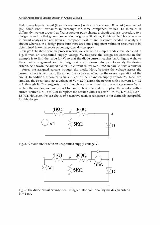
that, in any type of circuit (linear or nonlinear) with any operation (DC or AC) one can set (fix) some circuit variables in exchange for some component values. To think of it differently, we can argue that fixator-norator pairs change a circuit analysis procedure to a design procedure that guaranties certain design specifications, if obtainable. This is because in circuit analysis we are given all component values and resources needed to analyze a circuit; whereas, in a design procedure there are some component values or resources to be determined in exchange for achieving some design specs. Example 1: To show how the process works, we start with a simple diode circuit depicted in Fig. 5 with an unspecified supply voltage V1. Suppose the design requirement in this example is to find the value for V1 so that the diode current reaches 1mA. Figure 6 shows the circuit arrangement for this design using a fixator-norator pair to satisfy the design criteria. As shown, the added fixator -- a current source ID = 1 mA in parallel with a nullator -- forces the assigned current through the diode. Now, because the voltage across the current source is kept zero, the added fixator has no effect on the overall operation of the circuit. In addition, a norator is substituted for the unknown supply voltage V1. Next, we simulate the circuit and get a voltage of V1 = 2.2 V across the norator with a current I1 = 1.2 mA through it. This suggests that although we have aimed for the voltage source V1 to replace the norator, we have in fact two more choices to make: i) replace the norator with a current source I1 = 1.2 mA, or ii) replace the norator with a resistor R1 = -V1/I1 = -2.2/1.2 = -1.8 KΩ. However, the last choice of a negative (active) resistance is not definitely acceptable for this design.
5KΩ
300Ω
D
1KΩ
V1
1 2 3
Fig. 5. A diode circuit with an unspecified supply voltage V1
5KΩ
300Ω
D1mA
1KΩ
V1
1 2 34
Fig. 6. The diode circuit arrangement using a nullor pair to satisfy the design criteria ID = 1 mA
Advances in Analog Circuits
22
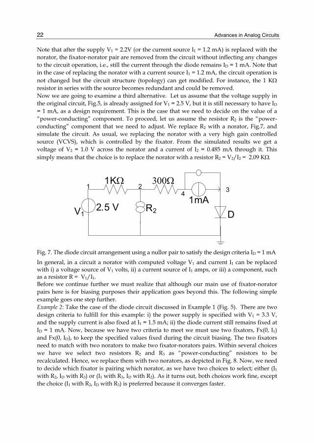
Note that after the supply V1 = 2.2V (or the current source I1 = 1.2 mA) is replaced with the norator, the fixator-norator pair are removed from the circuit without inflecting any changes to the circuit operation, i.e., still the current through the diode remains ID = 1 mA. Note that in the case of replacing the norator with a current source I1 = 1.2 mA, the circuit operation is not changed but the circuit structure (topology) can get modified. For instance, the 1 KΩ resistor in series with the source becomes redundant and could be removed. Now we are going to examine a third alternative. Let us assume that the voltage supply in the original circuit, Fig.5, is already assigned for V1 = 2.5 V, but it is still necessary to have ID = 1 mA, as a design requirement. This is the case that we need to decide on the value of a “power-conducting” component. To proceed, let us assume the resistor R2 is the “power-conducting” component that we need to adjust. We replace R2 with a norator, Fig.7, and simulate the circuit. As usual, we replacing the norator with a very high gain controlled source (VCVS), which is controlled by the fixator. From the simulated results we get a voltage of V2 = 1.0 V across the norator and a current of I2 = 0.485 mA through it. This simply means that the choice is to replace the norator with a resistor R2 = V2/I2 = 2.09 KΩ.
300Ω
D1mA
1KΩ
V1
1 2 34
R22.5 V
Fig. 7. The diode circuit arrangement using a nullor pair to satisfy the design criteria ID = 1 mA
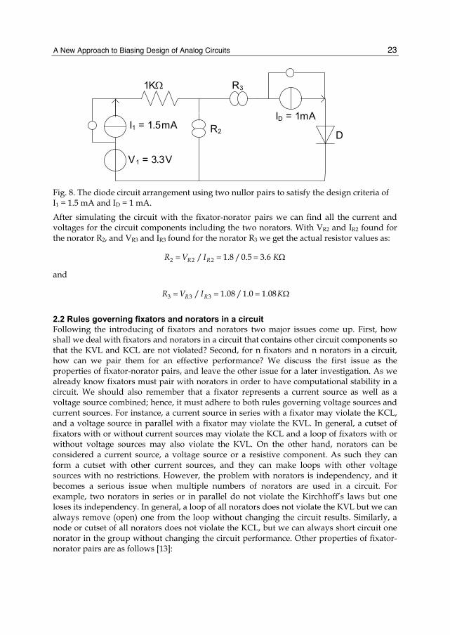
In general, in a circuit a norator with computed voltage V1 and current I1 can be replaced with i) a voltage source of V1 volts, ii) a current source of I1 amps, or iii) a component, such as a resistor R = V1/I1. Before we continue further we must realize that although our main use of fixator-norator pairs here is for biasing purposes their application goes beyond this. The following simple example goes one step further. Example 2: Take the case of the diode circuit discussed in Example 1 (Fig. 5). There are two design criteria to fulfill for this example: i) the power supply is specified with V1 = 3.3 V, and the supply current is also fixed at I1 = 1.5 mA; ii) the diode current still remains fixed at ID = 1 mA. Now, because we have two criteria to meet we must use two fixators, Fx(0, I1) and Fx(0, ID), to keep the specified values fixed during the circuit biasing. The two fixators need to match with two norators to make two fixator-norators pairs. Within several choices we have we select two resistors R2 and R3 as “power-conducting” resistors to be recalculated. Hence, we replace them with two norators, as depicted in Fig. 8. Now, we need to decide which fixator is pairing which norator, as we have two choices to select; either (I1 with R2, ID with R3) or (I1 with R3, ID with R2). As it turns out, both choices work fine, except the choice (I1 with R2, ID with R3) is preferred because it converges faster.
A New Approach to Biasing Design of Analog Circuits
23
D
1KΩ
ID = 1mAI1 = 1.5mA
V1 = 3.3V
R2
R3
Fig. 8. The diode circuit arrangement using two nullor pairs to satisfy the design criteria of I1 = 1.5 mA and ID = 1 mA.
After simulating the circuit with the fixator-norator pairs we can find all the current and voltages for the circuit components including the two norators. With VR2 and IR2 found for the norator R2, and VR3 and IR3 found for the norator R3 we get the actual resistor values as:
2 2 2/ 1.8 /0.5 3.6R RR V I K= = = Ω
and
3 3 3/ 1.08 /1.0 1.08R RR V I K= = = Ω
2.2 Rules governing fixators and norators in a circuit Following the introducing of fixators and norators two major issues come up. First, how shall we deal with fixators and norators in a circuit that contains other circuit components so that the KVL and KCL are not violated? Second, for n fixators and n norators in a circuit, how can we pair them for an effective performance? We discuss the first issue as the properties of fixator-norator pairs, and leave the other issue for a later investigation. As we already know fixators must pair with norators in order to have computational stability in a circuit. We should also remember that a fixator represents a current source as well as a voltage source combined; hence, it must adhere to both rules governing voltage sources and current sources. For instance, a current source in series with a fixator may violate the KCL, and a voltage source in parallel with a fixator may violate the KVL. In general, a cutset of fixators with or without current sources may violate the KCL and a loop of fixators with or without voltage sources may also violate the KVL. On the other hand, norators can be considered a current source, a voltage source or a resistive component. As such they can form a cutset with other current sources, and they can make loops with other voltage sources with no restrictions. However, the problem with norators is independency, and it becomes a serious issue when multiple numbers of norators are used in a circuit. For example, two norators in series or in parallel do not violate the Kirchhoff’s laws but one loses its independency. In general, a loop of all norators does not violate the KVL but we can always remove (open) one from the loop without changing the circuit results. Similarly, a node or cutset of all norators does not violate the KCL, but we can always short circuit one norator in the group without changing the circuit performance. Other properties of fixator-norator pairs are as follows [13]:
Advances in Analog Circuits
24
• The power consumed in a fixator Fx(V, I) is P = V*I; and the power is delivered by only one of the sources, V (for Fx(V, I) ) or I (for Fx(I, V) ).
• A resistance R in series with a fixator Fx(V, I) is absorbed by the fixator and the fixator becomes Fx(V1, I), where V1 = V + R*I. A resistance R in parallel with a fixator Fx(V, I) is absorbed by the fixator and the fixator becomes Fx(V, I1) ; where I1 = I + V/R.
• A current source IS in parallel with a fixator Fx(V, I) is absorbed by the fixator and the fixator becomes Fx(V, I1) , where I1 = I + IS.
• A voltage source VS in series with a fixator Fx(V, I) is absorbed by the fixator and the fixator becomes Fx(V1, I) , where V1 = V + VS.
• Connecting a fixator Fx(V, 0) across a port with the port voltage V does not affect the operation of the circuit; it only fixes the port voltage.
• Connecting a fixator Fx(0, I) in series with any component in a circuit with current I does not affect the operation of the circuit; it only fixes the current going through that component.
• In general, any two-terminal element in series with a fixator losses it’s current to the fixator; and any two-terminal element in parallel with a fixator losses its voltage to the fixator.
• A current source in series with a norator absorbs the norator; and a voltage source in parallel with a norator absorbs the norator. In addition, a current source in parallel with a norator is absorbed by the norator; and a voltage source in series with a norator is absorbed by the norator.
• A resistance in series or in parallel with a norator is absorbed by the norator. • A norator in series with a fixator Fx(V, I) becomes a current source I; and a norator in
parallel with a fixator Fx(V, I) becomes a voltage source V.
3. Circuit solutions containing fixator-norator pairs 3.1 Selective biasing Selective biasing is a procedure that fixes part of or the entire operating regions of a nonlinear component (say a transistor) during the circuit operation. To fix a biasing current, I, in a port we can use a fixator Fx(0, I). Similarly, to fix a biasing voltage, V, across a port we can use a fixator Fx(V, 0). However, as we discussed earlier, the use of fixators alone is not permissible in a circuit; we must pair each with a norator. On the other hand, both fixators Fx(0, I) and Fx(V, 0) carry zero power; hence, they alone cannot provide the biasing power to the serving component they are attached to. This simply means that for each fixator that is used to anchor certain biasing value in a circuit we need to provide the supplying power and direct it to the component. Our solution is either i) find a location for the supply power (voltage or current) and have the circuit find its magnitude, or ii) route the required power from an existing power supply through a power-conducting component. As it turns out the norators paring with the fixators can do both, provided that the pair are mutually sensitive, i.e., change in one causes the other to change accordingly.
3.2 Sensitivity in fixator-norator pairs In a circuit, each fixator can only work with a norator in a pair. A norator can be a source of power, a consumer of power or a power-conducting component. This means a norator must share power with a port that is anchored by a fixator. However, to satisfy this property the
A New Approach to Biasing Design of Analog Circuits
25
following condition must hold. A fixator paring with a norator must be “sensitive” to the changes happening in the norator and vice versa. This simply means that between a fixator and its pairing norator there must be a feedback. We can think of a norator as a placeholder for a DC supply or a power conductor in the circuit that must somehow “reach” to the corresponding fixator. In a way, when we replace a transistor port with its fixator model, we are getting a ticket, in exchange, to assign a DC source in the circuit wherever we like. This is true provided that the DC source is “reachable” by the fixator. Apparently, considering this property the choice of a norator pairing a fixator is not unique. In a connected circuit a (voltage or current) change within a component normally causes (voltage or current) changes throughout the circuit, although there are exceptions, particularly in cases of controlled sources without feedback. Therefore, in pairing a fixator with a norator we may have multiple numbers of choices to make; only avoiding those with zero feedback. This brings us to another issue, mentioned earlier, that can be stated as follows: for n fixators and n norators in a circuit how can we pair them for an effective design performance? This is certainly a challenging problem and we do not intend to make a comprehensive study on the subject here. What we would like to address is to find an acceptable relationship between a fixator and a norator in a pair so that it helps to speed up the biasing process in a circuit. The core issue in this relationship is the “sensitivity” issue [14, 15]. Simulating fixator-norator pairs - Before we continue further on the sensitivity issue we need to know how we can analyze or design a circuit that has fixator-norator pairs. Or simply, how can we simulate a circuit that contains nullator-norator pairs? As far as we know the existing circuit simulators, such as SPICE, do not have the means to directly handle the cases [16, 17, 18]. Traditionally, transistors and high gain operational amplifiers have been used for the purpose, and have done the job fairly successfully within acceptable accuracies [7, 9, 12]. However, in our case the situation is different. The fixator-norator pairs are only used symbolically in a circuit in order to establish the design criteria we have adopted. They are acting as catalyst and will be removed after the biasing is established in the circuit. Hence, we can assume the pairs to be ideal in order to provide the component values accurately. Within circuit components acceptable by a circuit simulator such as SPICE, controlled sources with very high gains are the ideal candidates for the job. Now, the question is what type of controlled sources must be used to simulate fixator-norator pairs? Evidently, if a fixator is used to fix a specified current in a circuit component, the source replacing the corresponding norator must be controlled by the voltage across the fixator. Similarly, if a fixator is used to fix a specified voltage in the circuit, the source replacing the corresponding norator must be controlled by the current through the fixator. Finally, the choice of the controlled source itself can be arbitrary. For example, if the job is to find the supply voltage VCC in response to a fixed current IB in the circuit then the controlled source is a voltage controlled voltage source (VCVS). On the other hand, if in the previous case the supply voltage VCC is already specified but we need to know how much current, IC, is conducted from VCC, then we can use a voltage controlled current source (VCCS) to manage to find IC, instead.
3.3 Paring fixators and norators in a circuit As mentioned earlier, one of the conditions to pair a fixator with a norator is to have feedback from the norator to the fixator. The purpose of this feedback is to harness the
Advances in Analog Circuits
26
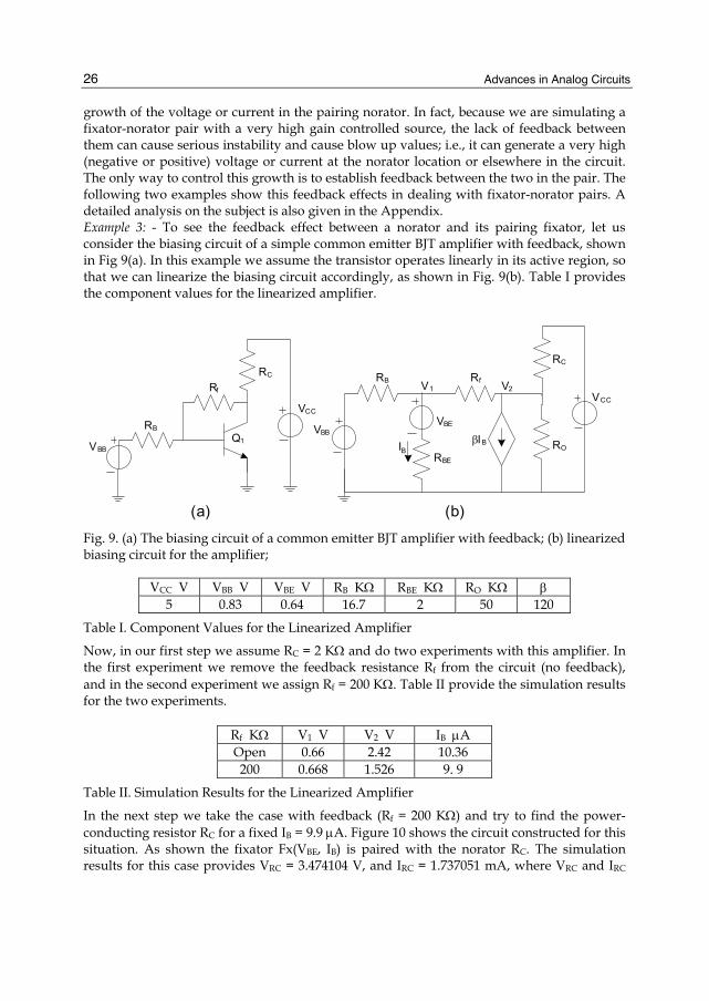
growth of the voltage or current in the pairing norator. In fact, because we are simulating a fixator-norator pair with a very high gain controlled source, the lack of feedback between them can cause serious instability and cause blow up values; i.e., it can generate a very high (negative or positive) voltage or current at the norator location or elsewhere in the circuit. The only way to control this growth is to establish feedback between the two in the pair. The following two examples show this feedback effects in dealing with fixator-norator pairs. A detailed analysis on the subject is also given in the Appendix. Example 3: - To see the feedback effect between a norator and its pairing fixator, let us consider the biasing circuit of a simple common emitter BJT amplifier with feedback, shown in Fig 9(a). In this example we assume the transistor operates linearly in its active region, so that we can linearize the biasing circuit accordingly, as shown in Fig. 9(b). Table I provides the component values for the linearized amplifier.
RB
VBB
VCC
RC
Rf
VBE
RORBE
IBβIB
RB
VCC
VBB
RC
Rf
Q1
(a) (b)
V1 V2
Fig. 9. (a) The biasing circuit of a common emitter BJT amplifier with feedback; (b) linearized biasing circuit for the amplifier;
VCC V VBB V VBE V RB KΩ RBE KΩ RO KΩ β 5 0.83 0.64 16.7 2 50 120
Table I. Component Values for the Linearized Amplifier
Now, in our first step we assume RC = 2 KΩ and do two experiments with this amplifier. In the first experiment we remove the feedback resistance Rf from the circuit (no feedback), and in the second experiment we assign Rf = 200 KΩ. Table II provide the simulation results for the two experiments.
Rf KΩ V1 V V2 V IB μA Open 0.66 2.42 10.36 200 0.668 1.526 9. 9
Table II. Simulation Results for the Linearized Amplifier
In the next step we take the case with feedback (Rf = 200 KΩ) and try to find the power-conducting resistor RC for a fixed IB = 9.9 μA. Figure 10 shows the circuit constructed for this situation. As shown the fixator Fx(VBE, IB) is paired with the norator RC. The simulation results for this case provides VRC = 3.474104 V, and IRC = 1.737051 mA, where VRC and IRC
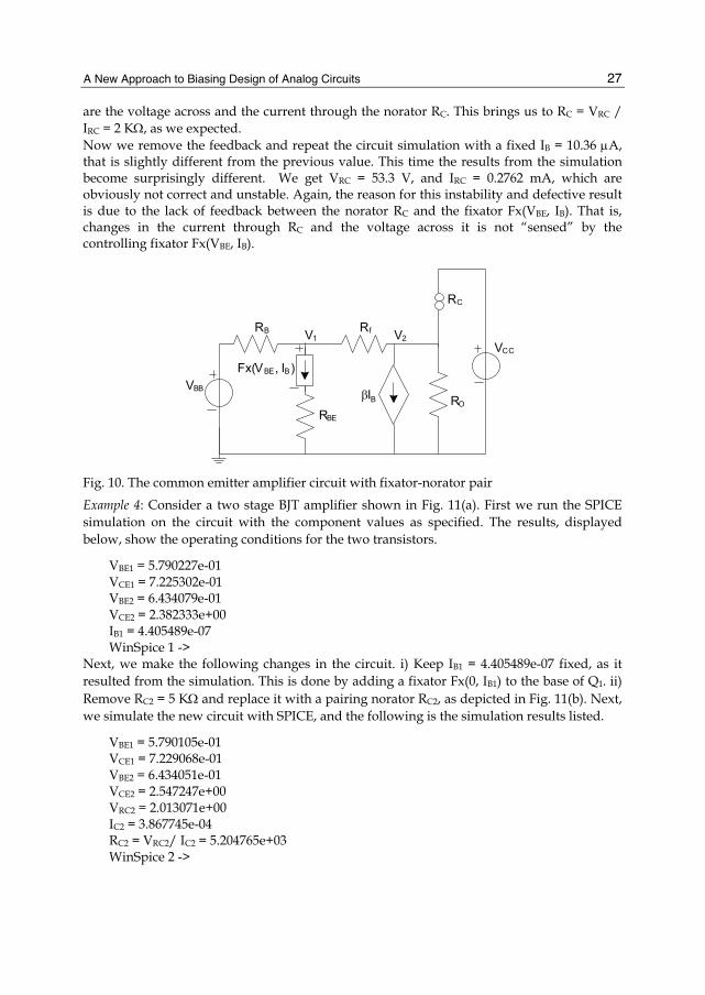
A New Approach to Biasing Design of Analog Circuits
27
are the voltage across and the current through the norator RC. This brings us to RC = VRC / IRC = 2 KΩ, as we expected. Now we remove the feedback and repeat the circuit simulation with a fixed IB = 10.36 μA, that is slightly different from the previous value. This time the results from the simulation become surprisingly different. We get VRC = 53.3 V, and IRC = 0.2762 mA, which are obviously not correct and unstable. Again, the reason for this instability and defective result is due to the lack of feedback between the norator RC and the fixator Fx(VBE, IB). That is, changes in the current through RC and the voltage across it is not “sensed” by the controlling fixator Fx(VBE, IB).
RB
VBB
VCC
RC
Rf
RORBE
βIB
V1 V2
Fx(VBE, IB)
Fig. 10. The common emitter amplifier circuit with fixator-norator pair
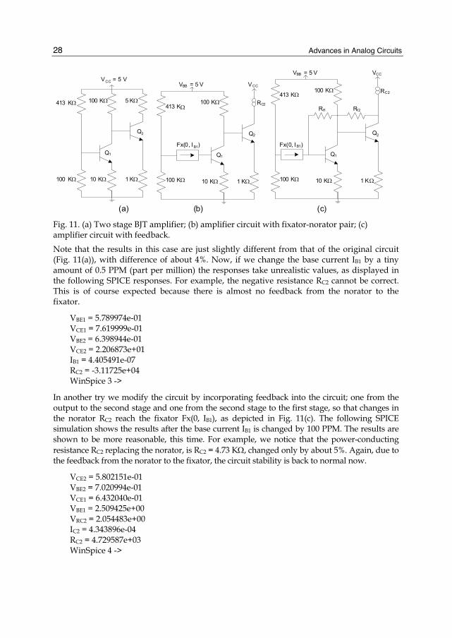
Example 4: Consider a two stage BJT amplifier shown in Fig. 11(a). First we run the SPICE simulation on the circuit with the component values as specified. The results, displayed below, show the operating conditions for the two transistors.
VBE1 = 5.790227e-01 VCE1 = 7.225302e-01 VBE2 = 6.434079e-01 VCE2 = 2.382333e+00 IB1 = 4.405489e-07 WinSpice 1 ->
Next, we make the following changes in the circuit. i) Keep IB1 = 4.405489e-07 fixed, as it resulted from the simulation. This is done by adding a fixator Fx(0, IB1) to the base of Q1. ii) Remove RC2 = 5 KΩ and replace it with a pairing norator RC2, as depicted in Fig. 11(b). Next, we simulate the new circuit with SPICE, and the following is the simulation results listed.
VBE1 = 5.790105e-01 VCE1 = 7.229068e-01 VBE2 = 6.434051e-01 VCE2 = 2.547247e+00 VRC2 = 2.013071e+00 IC2 = 3.867745e-04 RC2 = VRC2/ IC2 = 5.204765e+03 WinSpice 2 ->
Advances in Analog Circuits
28
(a) (b) (c)
413 KΩ
100 KΩ 10 KΩ 1 KΩ
100 KΩ 5 KΩ
VCC = 5 V
Q2
Q1
413 KΩ
100 KΩ 10 KΩ 1 KΩ
100 KΩ
VCC
Q2
Q1
RC2
Fx(0, IB1)
VBB = 5 V
413 KΩ
100 KΩ 10 KΩ 1 KΩ
100 KΩ
VCC
Q2
Q1
RC2
Fx(0, IB1)
VBB = 5 V
Rf1 Rf2
Fig. 11. (a) Two stage BJT amplifier; (b) amplifier circuit with fixator-norator pair; (c) amplifier circuit with feedback.
Note that the results in this case are just slightly different from that of the original circuit (Fig. 11(a)), with difference of about 4%. Now, if we change the base current IB1 by a tiny amount of 0.5 PPM (part per million) the responses take unrealistic values, as displayed in the following SPICE responses. For example, the negative resistance RC2 cannot be correct. This is of course expected because there is almost no feedback from the norator to the fixator.
VBE1 = 5.789974e-01 VCE1 = 7.619999e-01 VBE2 = 6.398944e-01 VCE2 = 2.206873e+01 IB1 = 4.405491e-07 RC2 = -3.11725e+04 WinSpice 3 ->
In another try we modify the circuit by incorporating feedback into the circuit; one from the output to the second stage and one from the second stage to the first stage, so that changes in the norator RC2 reach the fixator Fx(0, IB1), as depicted in Fig. 11(c). The following SPICE simulation shows the results after the base current IB1 is changed by 100 PPM. The results are shown to be more reasonable, this time. For example, we notice that the power-conducting resistance RC2 replacing the norator, is RC2 = 4.73 KΩ, changed only by about 5%. Again, due to the feedback from the norator to the fixator, the circuit stability is back to normal now.
VCE2 = 5.802151e-01 VBE2 = 7.020994e-01 VCE1 = 6.432040e-01 VBE1 = 2.509425e+00 VRC2 = 2.054483e+00 IC2 = 4.343896e-04 RC2 = 4.729587e+03 WinSpice 4 ->
A New Approach to Biasing Design of Analog Circuits
29
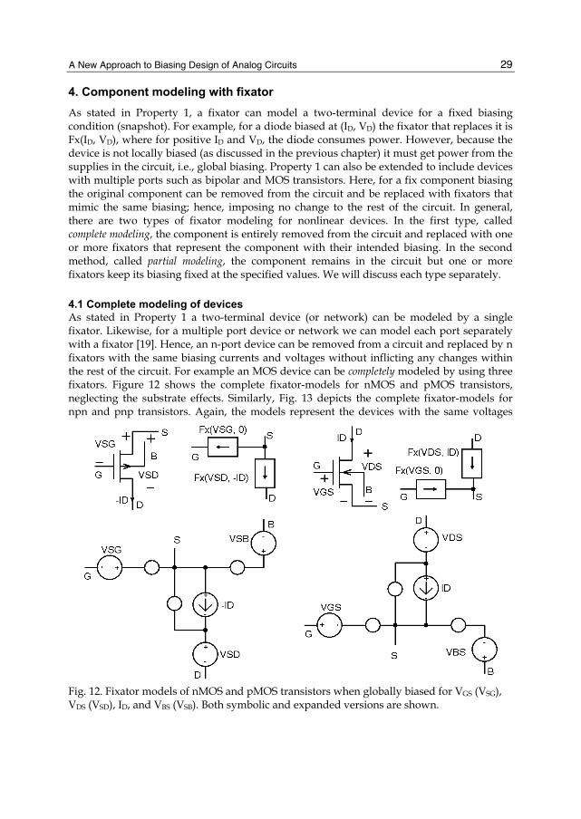
4. Component modeling with fixator As stated in Property 1, a fixator can model a two-terminal device for a fixed biasing condition (snapshot). For example, for a diode biased at (ID, VD) the fixator that replaces it is Fx(ID, VD), where for positive ID and VD, the diode consumes power. However, because the device is not locally biased (as discussed in the previous chapter) it must get power from the supplies in the circuit, i.e., global biasing. Property 1 can also be extended to include devices with multiple ports such as bipolar and MOS transistors. Here, for a fix component biasing the original component can be removed from the circuit and be replaced with fixators that mimic the same biasing; hence, imposing no change to the rest of the circuit. In general, there are two types of fixator modeling for nonlinear devices. In the first type, called complete modeling, the component is entirely removed from the circuit and replaced with one or more fixators that represent the component with their intended biasing. In the second method, called partial modeling, the component remains in the circuit but one or more fixators keep its biasing fixed at the specified values. We will discuss each type separately.
4.1 Complete modeling of devices As stated in Property 1 a two-terminal device (or network) can be modeled by a single fixator. Likewise, for a multiple port device or network we can model each port separately with a fixator [19]. Hence, an n-port device can be removed from a circuit and replaced by n fixators with the same biasing currents and voltages without inflicting any changes within the rest of the circuit. For example an MOS device can be completely modeled by using three fixators. Figure 12 shows the complete fixator-models for nMOS and pMOS transistors, neglecting the substrate effects. Similarly, Fig. 13 depicts the complete fixator-models for npn and pnp transistors. Again, the models represent the devices with the same voltages
Fig. 12. Fixator models of nMOS and pMOS transistors when globally biased for VGS (VSG), VDS (VSD), ID, and VBS (VSB). Both symbolic and expanded versions are shown.

Advances in Analog Circuits
30
Fig. 13. Fixator models of npn and pnp transistors when globally biased for VBE (VEB), VCE (VEC), and IC.
and currents that they need to get biased to the specified Q-points. Note that two changes are taking place in the circuit after the modeling is done: i) the resulted circuit becomes linear, and ii) the circuit is DC-freezed at fixed biasing conditions. What it means is that, addition (or removal) of any source or signal to the circuit may change signal conditions within the circuit but no change in inflicted on the modeled transistors. Hence, circuits with fixator-modeled components are not prepared for AC analysis.
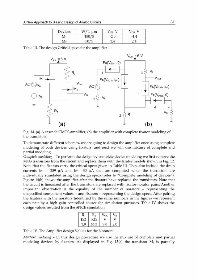
4.2 Partial modeling of devices In partial modeling the device remains biased in the circuit. In addition one or more fixators are used to freeze one or more device (port) variables at given Q-points. We have already used partial modeling in previous examples; for instance, in Example 4 we have freezed the base current IB1 of Q1 during the entire biasing process. The advantage here is that we can limit the number of fixators to the number of biasing specs provided for the design. Also, a limited number of fixators makes it easier to match the number of fixators with that of norators in the circuit. This helps to speed up the biasing procedure in a large circuit. Another advantage in using partial modeling is that, in partial modeling the fixators are only responsible to provide some critical biasing requirements and the rest are left to the actual device, placed in the circuit, to adjust. For example, in a bipolar transistor only base current IB and the collector-emitter voltage VCE might be considered critical; because with IB given the transistor will decide on the value of VBE. Similarly, with the gain factor β known the collector current IC is automatically established through the device characteristics. However, the disadvantage here is that the circuit remains nonlinear. In contrast with partial modeling, in complete modeling the transistors are totally absent from the circuit and have been replaced with the fixators. This means the fixators are fully in charge to accurately place the Q-points on the characteristic curves. This produces an extra work for the designer, who, prior to the actual design, needs to run the transistors individually and record the port values for the Q-points he/she has in mind. Then he/she needs to place the port values into the fixators and exchange the fixators with the corresponding transistors for the actual design. The third option is to have a mixture of the two; i.e., some transistors get complete modeling by fixators, while others are partially modeled. However, we are not allowed to have partial modeling on a port of a transistor and apply complete modeling on another port of the same transistor for obvious reasons. Example 5: The objective in this example is to design a cascade CMOS amplifier, shown in Fig. 14(a). The transistor sizes and the critical specs given for the design are listed in Table III.
A New Approach to Biasing Design of Analog Circuits
31
Devices W/L μm VGS V VDS V M1 150/5 -2.0 -4.4 M2 50/5 1.4 2.4
Table III. The design Critical specs for the amplifier
AC
VB
VDD = 5 V
VI
M1
vin M2
Vout
R2
R1
AC
VDD = 5 V
R1
R2
Vout
VB
VI
Fx(VSD1, ID1)
Fx(VDS2, ID2)
Fx(VSG 1, 0)
Fx(VGS2, 0)
(a) (b)
1
1
2
2
3
3
44
Fig. 14. (a) A cascade CMOS amplifier; (b) the amplifier with complete fixator modeling of the transistors.
To demonstrate different schemes, we are going to design the amplifier once using complete modeling of both devices using fixators, and next we will use mixture of complete and partial modeling. Complete modeling – To perform the design by complete device modeling we first remove the MOS transistors from the circuit and replace them with the fixator models shown in Fig. 12. Note that the fixators carry the critical specs given in Table III. They also include the drain currents ID1 = 289 μA and ID2 =30 μA that are computed when the transistors are individually simulated using the design specs (refer to “Complete modeling of devices”). Figure 14(b) shows the amplifier after the fixators have replaced the transistors. Note that the circuit is linearized after the transistors are replaced with fixator-norator pairs. Another important observation is the equality of the number of norators -- representing the unspecified component values -- and fixators -- representing the design specs. After pairing the fixators with the norators (identified by the same numbers in the figure) we represent each pair by a high gain controlled source for simulation purposes. Table IV shows the design values resulted from the SPICE simulation.
R1 KΩ
R2
KΩ VGG
V VB V
1.9 66.3 3.0 2.0
Table IV. The Amplifier design Values for the Norators
Mixture modeling – In this design procedure we use the mixture of complete and partial modeling devices by fixators. As displayed in Fig. 15(a) the transistor M1 is partially
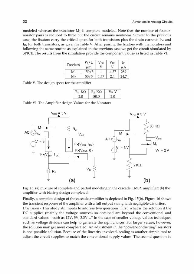
Advances in Analog Circuits
32
modeled whereas the transistor M2 is complete modeled. Note that the number of fixator-norator pairs is reduced to three but the circuit remains nonlinear. Similar to the previous case, the fixators carry the critical specs for both transistors plus the drain currents ID1 and ID2 for both transistors, as given in Table V. After pairing the fixators with the norators and following the same routine as explained in the previous case we get the circuit simulated by SPICE. The results from the simulation provide the component values as listed in Table VI.
Devices W/L μm
VGS V
VDS V
ID μA
M1 150/5 - -4.37 289 M2 50/5 1.37 2.4 24.7
Table V. The design specs for the amplifier
R1 KΩ R2 KΩ VB V 2.0 80.0 2.0
Table VI. The Amplifier design Values for the Norators
VDD = 5 V
AC
VI = 3 V
M1
vin
Fx(VDS2, ID2)
Fx(VGS2, 0) Fx(VSD1, ID1)
R1VB
R2
Vout
AC
2 KΩ
80 KΩ
VB = 2 V
VDD = 5 V
VI = 3 V
M1
vin M2
Vout
(a) (b) Fig. 15. (a) mixture of complete and partial modeling in the cascade CMOS amplifier; (b) the amplifier with biasing design completed.
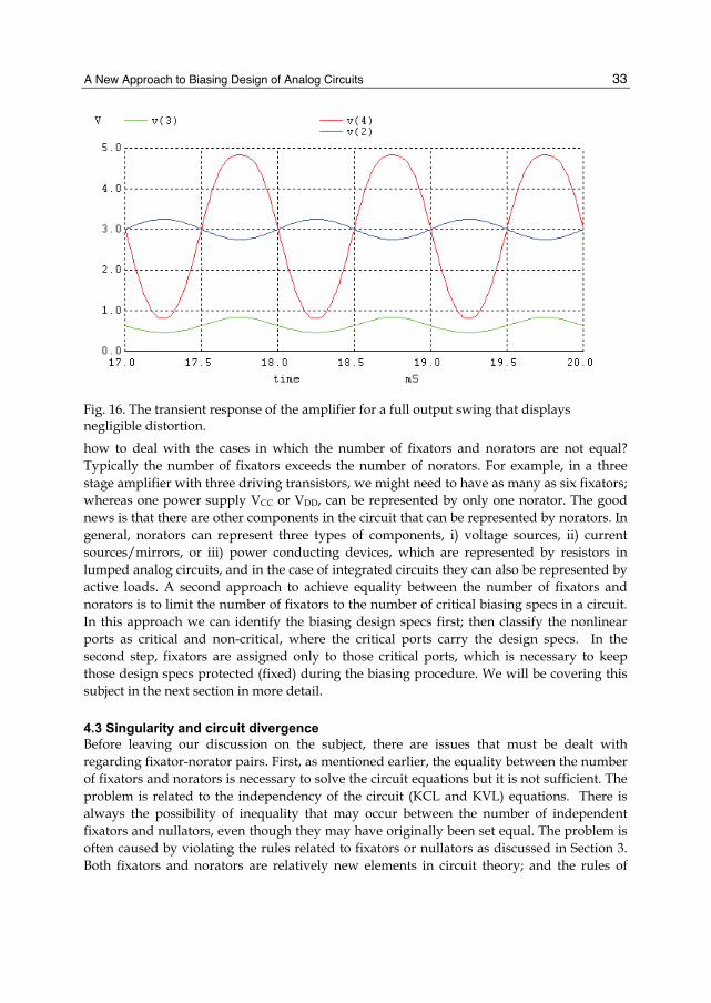
Finally, a complete design of the cascade amplifier is depicted in Fig. 15(b). Figure 16 shows the transient response of the amplifier with a full output swing with negligible distortion. Discussion - This study still needs to address two questions. First, what is the solution if the DC supplies (mainly the voltage sources) so obtained are beyond the conventional and standard values – such as 12V, 5V, 3.3V…? In the case of smaller voltage values techniques such as voltage dividers can help to generate the right choices. For larger values, however, the solution may get more complecated. An adjustment in the “power-conducting” resistors is one possible solution. Because of the linearity involved, scaling is another simple tool to adjust the circuit supplies to match the conventional supply values. The second question is:
A New Approach to Biasing Design of Analog Circuits
33
Fig. 16. The transient response of the amplifier for a full output swing that displays negligible distortion.
how to deal with the cases in which the number of fixators and norators are not equal? Typically the number of fixators exceeds the number of norators. For example, in a three stage amplifier with three driving transistors, we might need to have as many as six fixators; whereas one power supply VCC or VDD, can be represented by only one norator. The good news is that there are other components in the circuit that can be represented by norators. In general, norators can represent three types of components, i) voltage sources, ii) current sources/mirrors, or iii) power conducting devices, which are represented by resistors in lumped analog circuits, and in the case of integrated circuits they can also be represented by active loads. A second approach to achieve equality between the number of fixators and norators is to limit the number of fixators to the number of critical biasing specs in a circuit. In this approach we can identify the biasing design specs first; then classify the nonlinear ports as critical and non-critical, where the critical ports carry the design specs. In the second step, fixators are assigned only to those critical ports, which is necessary to keep those design specs protected (fixed) during the biasing procedure. We will be covering this subject in the next section in more detail.
4.3 Singularity and circuit divergence Before leaving our discussion on the subject, there are issues that must be dealt with regarding fixator-norator pairs. First, as mentioned earlier, the equality between the number of fixators and norators is necessary to solve the circuit equations but it is not sufficient. The problem is related to the independency of the circuit (KCL and KVL) equations. There is always the possibility of inequality that may occur between the number of independent fixators and nullators, even though they may have originally been set equal. The problem is often caused by violating the rules related to fixators or nullators as discussed in Section 3. Both fixators and norators are relatively new elements in circuit theory; and the rules of
Advances in Analog Circuits
34
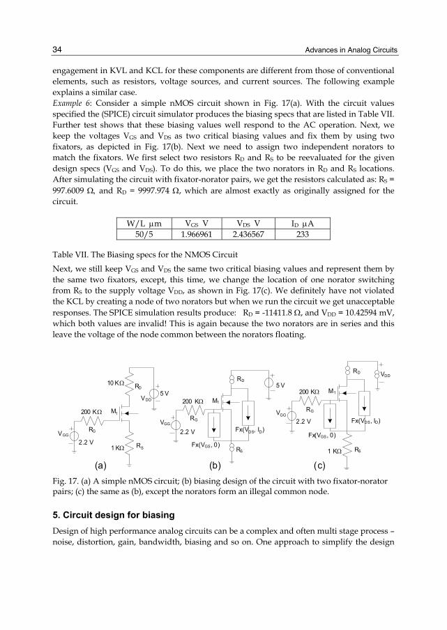
engagement in KVL and KCL for these components are different from those of conventional elements, such as resistors, voltage sources, and current sources. The following example explains a similar case. Example 6: Consider a simple nMOS circuit shown in Fig. 17(a). With the circuit values specified the (SPICE) circuit simulator produces the biasing specs that are listed in Table VII. Further test shows that these biasing values well respond to the AC operation. Next, we keep the voltages VGS and VDS as two critical biasing values and fix them by using two fixators, as depicted in Fig. 17(b). Next we need to assign two independent norators to match the fixators. We first select two resistors RD and RS to be reevaluated for the given design specs (VGS and VDS). To do this, we place the two norators in RD and RS locations. After simulating the circuit with fixator-norator pairs, we get the resistors calculated as: RS = 997.6009 Ω, and RD = 9997.974 Ω, which are almost exactly as originally assigned for the circuit.
W/L μm VGS V VDS V ID μA 50/5 1.966961 2.436567 233
Table VII. The Biasing specs for the NMOS Circuit
Next, we still keep VGS and VDS the same two critical biasing values and represent them by the same two fixators, except, this time, we change the location of one norator switching from RS to the supply voltage VDD, as shown in Fig. 17(c). We definitely have not violated the KCL by creating a node of two norators but when we run the circuit we get unacceptable responses. The SPICE simulation results produce: RD = -11411.8 Ω, and VDD = 10.42594 mV, which both values are invalid! This is again because the two norators are in series and this leave the voltage of the node common between the norators floating.
(a) (b)
5 V
200 KΩ M1
RD
RG
RS 1 KΩ
10 KΩ
VDD
VGG
2.2 V
5 V
200 KΩ M1
RD
RG
RS
VGG
2.2 V
Fx(VGS, 0)
Fx(VDS, ID)
200 KΩ M1
RD
RG
RS
VGG
2.2 V
Fx(VGS, 0)
Fx(VDS, ID)
VDD
1 KΩ
(c) Fig. 17. (a) A simple nMOS circuit; (b) biasing design of the circuit with two fixator-norator pairs; (c) the same as (b), except the norators form an illegal common node.
5. Circuit design for biasing Design of high performance analog circuits can be a complex and often multi stage process – noise, distortion, gain, bandwidth, biasing and so on. One approach to simplify the design
A New Approach to Biasing Design of Analog Circuits
35
and cut loops and feedbacks between the stages is to use as much orthogonality as possible [3]. This orthogonality is practiced in this chapter, between the circuit performances and the biasing of the nonlinear components, or simply between AC and DC circuit designs. The first task is to design for the circuit performances, mainly noise, signal power, and bandwidth [3]. The biasing design typically comes last, except for possible circuit modification that may require us to go back to the performance design, repeatedly. We only deal with the biasing situation in this chapter. A full discussion on the performance design and other related circuit design issues can be found in the literature [3]. Our approach to designing analog circuit biasing starts with a circuit topology (structure) that is suitable for the design. There is, of course, no restriction on this topology and structural modifications are acceptable during the design, as long as the final structure can fulfill the design criteria. In case the circuit structure for the performance design is different from that of the biasing design -- such as those with coupling or bypass capacitors -- we restrict ourselves only to the bias (DC) handling structure. Our next move is to select regions of operations for the transistors that fulfill the design requirements. This step may need some individual testing of the transistors to make sure of their behavior in the circuit. In the third step, and because the operating points for the transistors are specified, the components can be replaced with their small signal linear models; and here is where the performance (AC) design can start and continue until the design criteria are met. Following the performance design we need to bias the components in the circuit so that each one operates at the regions (Q-points) specified by the circuit performances. Algorithm 1 provides a systematic procedure to do the circuit biasing using fixator-norator pairs.
5.1 Algorithm 1: Preparation - Given the design specification, we begin with the performance design by selecting a working circuit topology. We then choose the desired operating points for the drivers3 that best meet the design requirements. Then we replace all the transistors with their small signal linear models, to make the circuit entirely linear and ready for the AC design. Note that as long as the linear models, representing locally biased devices, are not altered the circuit topology as well as the component values (including the W/L ratios in MOS transistors) can be changed for an optimal performance of the circuit. Finally, upon the completion of the performance (AC) design, we can start the biasing design as follows: 1. Assign one fixator, carrying the biasing spec, to each “critical” transistor port. Also
assign one norator to a location in the circuit that is a candidate for i) a DC supply voltage, b) a DC supply current, or iii) a power-conducting component such as a resistor. Note: be sure that the number of fixators and norators match.
2. Pair each fixator with a norator in the circuit. This step is rather critical and needs to be handled with care (see Sensitivity in fixator-norator pairs in Section 3). In general, any pair must work (although may not be optimal), except for the cases where a fixator is not sensitive to the changes in the norator.
3 In amplifiers drivers are the circuit transistors that are along the signal path and are directly involved in circuit performance. Other non-driver transistors may exist in the circuit, such as those used in active loads or current mirrors.

Advances in Analog Circuits
36
3. Assign one controlled source with high gain to each pair of fixator-norator so that the fixator controls the source at the norator location. It is permissible to assume an ideal controlled source with very high gain; this is because these controlled sources will disappear afterwards, leaving the actual DC supplies or power-conducting components in place. A controlled source can be one of the four types: VCVS, VCCS, CCVS, or CCCS. The choice depends on the individual situation as follows: a. For a fixator keeping a specified current fixed the controlled source is either VCVS,
or VCCS. b. For a fixator keeping a specified voltage fixed the controlled source is either CCVS,
or CCCS. c. For a norator holding the place for a voltage supply the best choice is either a
VCVS, or CCVS. d. For a norator holding the place for a current (mirror) supply the best choice is
either a VCCS, or CCCS. e. For a norator holding the place for a power-conducting component any of the four
will work. 4. Solve the linear circuit equations as prepared. The DC solution (simulation) provides
the currents and voltages for the circuit components including those of the norators that are represented by the controlled sources.
5. Remove all the controlled sources from the circuit and replace each with an appropriate voltage supply, Vj, a current supply, Ij, or a resistor Rj = Vj,/Ij; where Vj and Ij are the voltage and current found for that controlled source (norator).
This concludes the biasing design algorithm.
6. Design examples The following examples provide a systematic procedure for biasing design of analog circuits using the new approach, given in Algorithm 1. Example 7: This example presents a negative feedback BJT amplifier; fully explained in reference [3]. Figure 18 shows a simplified AC schematic of the amplifier after it has gone through the performance design in three areas: noise reduction, clipping/distortion reduction, and high loop-gain-poles-product4. To perform the biasing of the circuit we need to first specify the values of the DC supplies and their locations in the circuit. Next, we need to select the operating points for the transistors so that they can fulfill the design specs. For the actual power supplies, we choose two DC sources of 4V and - 4V, as assigned in the reference [3]. Next we need to select DC power-conducting components that provide biasing power to the drivers. However, there are certain performance design criteria that must be given priority in this selection so that the biasing is smoothly aligned with the rest of the design. These major performance design criteria are as follows: • The emitters of Q1 and Q2 must be driven by a high impedance current source, Ie. • The base of Q2 must be driven by a low impedance voltage source, Vb2. • The collector of Q1 can be driven directly by VCC.
4 For details please refer to Chapter 10 in [3].
A New Approach to Biasing Design of Analog Circuits
37
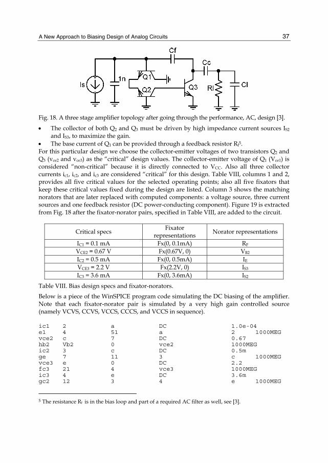
Fig. 18. A three stage amplifier topology after going through the performance, AC, design [3].
• The collector of both Q2 and Q3 must be driven by high impedance current sources IS2 and IS3, to maximize the gain.
• The base current of Q1 can be provided through a feedback resistor Rf5. For this particular design we choose the collector-emitter voltages of two transistors Q2 and Q3 (vce2 and vce3) as the “critical” design values. The collector-emitter voltage of Q1 (Vce1) is considered “non-critical” because it is directly connected to VCC. Also all three collector currents ic1, ic2, and ic3 are considered “critical” for this design. Table VIII, columns 1 and 2, provides all five critical values for the selected operating points; also all five fixators that keep these critical values fixed during the design are listed. Column 3 shows the matching norators that are later replaced with computed components: a voltage source, three current sources and one feedback resistor (DC power-conducting component). Figure 19 is extracted from Fig. 18 after the fixator-norator pairs, specified in Table VIII, are added to the circuit.
Critical specs Fixator representations Norator representations
IC1 = 0.1 mA Fx(0, 0.1mA) RF VCE2 = 0.67 V Fx(0.67V, 0) VB2 IC2 = 0.5 mA Fx(0, 0.5mA) IE VCE3 = 2.2 V Fx(2.2V, 0) IS3 IC3 = 3.6 mA Fx(0, 3.6mA) IS2
Table VIII. Bias design specs and fixator-norators.
Below is a piece of the WinSPICE program code simulating the DC biasing of the amplifier. Note that each fixator-norator pair is simulated by a very high gain controlled source (namely VCVS, CCVS, VCCS, CCCS, and VCCS in sequence). ic1 2 a DC 1.0e-04 e1 4 51 a 2 1000MEG vce2 c 7 DC 0.67 hb2 Vb2 0 vce2 1000MEG ic2 3 c DC 0.5m ge 7 11 3 c 1000MEG vce3 e 0 DC 2.2 fc3 21 4 vce3 1000MEG ic3 4 e DC 3.6m gc2 12 3 4 e 1000MEG
5 The resistance Rf is in the bias loop and part of a required AC filter as well, see [3].
Advances in Analog Circuits
38
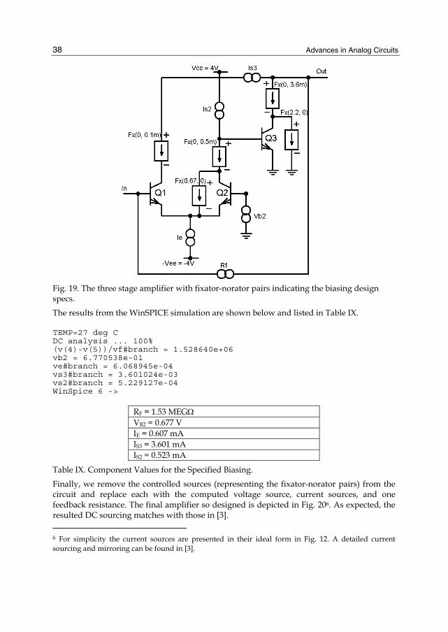
Fig. 19. The three stage amplifier with fixator-norator pairs indicating the biasing design specs.
The results from the WinSPICE simulation are shown below and listed in Table IX. TEMP=27 deg C DC analysis ... 100% (v(4)-v(5))/vf#branch = 1.528640e+06 vb2 = 6.770538e-01 ve#branch = 6.068945e-04 vs3#branch = 3.601024e-03 vs2#branch = 5.229127e-04 WinSpice 6 ->
RF = 1.53 MEGΩ VB2 = 0.677 V IE = 0.607 mA IS3 = 3.601 mA IS2 = 0.523 mA
Table IX. Component Values for the Specified Biasing.
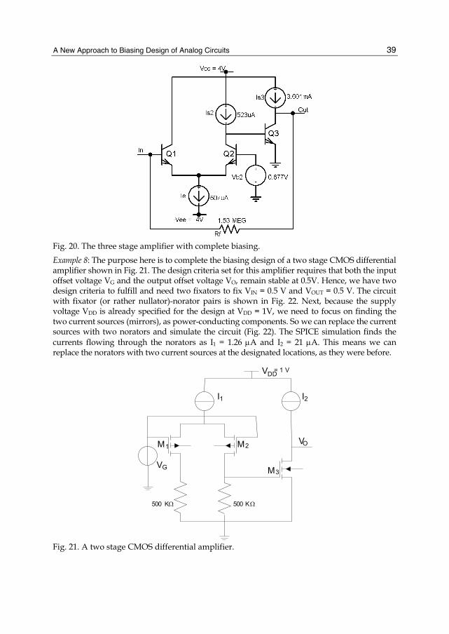
Finally, we remove the controlled sources (representing the fixator-norator pairs) from the circuit and replace each with the computed voltage source, current sources, and one feedback resistance. The final amplifier so designed is depicted in Fig. 206. As expected, the resulted DC sourcing matches with those in [3]. 6 For simplicity the current sources are presented in their ideal form in Fig. 12. A detailed current sourcing and mirroring can be found in [3].
A New Approach to Biasing Design of Analog Circuits
39
Fig. 20. The three stage amplifier with complete biasing. Example 8: The purpose here is to complete the biasing design of a two stage CMOS differential amplifier shown in Fig. 21. The design criteria set for this amplifier requires that both the input offset voltage VG and the output offset voltage VO, remain stable at 0.5V. Hence, we have two design criteria to fulfill and need two fixators to fix VIN = 0.5 V and VOUT = 0.5 V. The circuit with fixator (or rather nullator)-norator pairs is shown in Fig. 22. Next, because the supply voltage VDD is already specified for the design at VDD = 1V, we need to focus on finding the two current sources (mirrors), as power-conducting components. So we can replace the current sources with two norators and simulate the circuit (Fig. 22). The SPICE simulation finds the currents flowing through the norators as I1 = 1.26 μA and I2 = 21 μA. This means we can replace the norators with two current sources at the designated locations, as they were before.
500 KΩ500 KΩ
M
MM1 2
3
DD
G
V
V
= 1 V
I I1 2
OV
Fig. 21. A two stage CMOS differential amplifier.
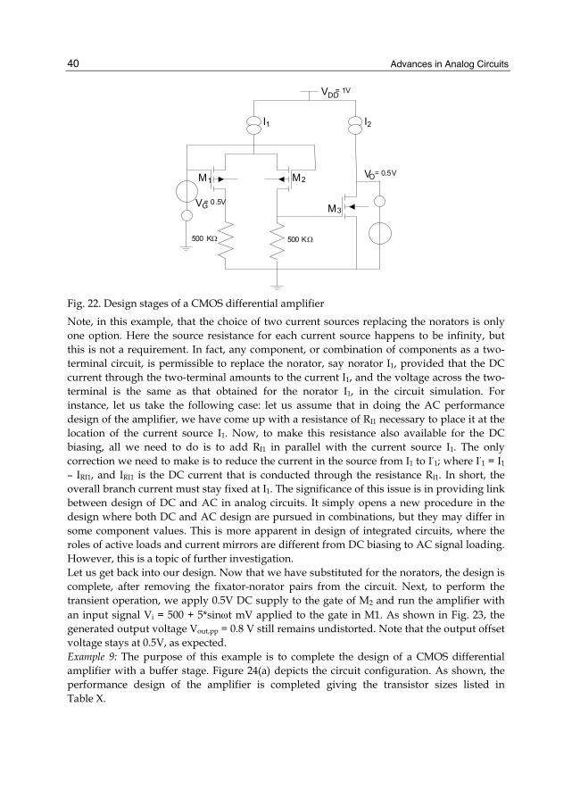
Advances in Analog Circuits
40
500 KΩ500 KΩ
M
MM1 2
3
DDV = 1V
I1 I2
GV = 0.5V
OV = 0.5V
Fig. 22. Design stages of a CMOS differential amplifier
Note, in this example, that the choice of two current sources replacing the norators is only one option. Here the source resistance for each current source happens to be infinity, but this is not a requirement. In fact, any component, or combination of components as a two-terminal circuit, is permissible to replace the norator, say norator I1, provided that the DC current through the two-terminal amounts to the current I1, and the voltage across the two-terminal is the same as that obtained for the norator I1, in the circuit simulation. For instance, let us take the following case: let us assume that in doing the AC performance design of the amplifier, we have come up with a resistance of RI1 necessary to place it at the location of the current source I1. Now, to make this resistance also available for the DC biasing, all we need to do is to add RI1 in parallel with the current source I1. The only correction we need to make is to reduce the current in the source from I1 to I’1; where I’1 = I1 – IRI1, and IRI1 is the DC current that is conducted through the resistance RI1. In short, the overall branch current must stay fixed at I1. The significance of this issue is in providing link between design of DC and AC in analog circuits. It simply opens a new procedure in the design where both DC and AC design are pursued in combinations, but they may differ in some component values. This is more apparent in design of integrated circuits, where the roles of active loads and current mirrors are different from DC biasing to AC signal loading. However, this is a topic of further investigation. Let us get back into our design. Now that we have substituted for the norators, the design is complete, after removing the fixator-norator pairs from the circuit. Next, to perform the transient operation, we apply 0.5V DC supply to the gate of M2 and run the amplifier with an input signal Vi = 500 + 5*sinωt mV applied to the gate in M1. As shown in Fig. 23, the generated output voltage Vout,pp = 0.8 V still remains undistorted. Note that the output offset voltage stays at 0.5V, as expected. Example 9: The purpose of this example is to complete the design of a CMOS differential amplifier with a buffer stage. Figure 24(a) depicts the circuit configuration. As shown, the performance design of the amplifier is completed giving the transistor sizes listed in Table X.
A New Approach to Biasing Design of Analog Circuits
41
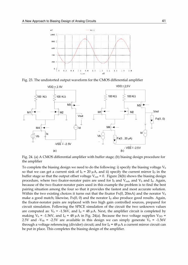
Fig. 23. The undistorted output waveform for the CMOS differential amplifier
Vout
100 KΩ
Id
Vb
VDD = 2.5V
M1
-VSS = -2.5V
100 KΩ
M2
M3
M4
Is
Vout
100 KΩ
IdVb
VDD = 2.5V
M1
- VSS = -2.5V
100 KΩ
M2
M3
M4
Fx(0 , 0)
Fx(0 , 20 μA)
(a) (b) Fig. 24. (a) A CMOS differential amplifier with buffer stage; (b) biasing design procedure for the amplifier
To complete the biasing design we need to do the following: i) specify the biasing voltage Vb so that we can get a current sink of IS = 20 μA, and ii) specify the current mirror ID in the buffer stage so that the output offset voltage Vout = 0. Figure 24(b) shows the biasing design procedure, where two fixator-norator pairs are used for IS and Vout, and Vb and Id. Again, because of the two fixator-norator pairs used in this example the problem is to find the best pairing situation among the four so that it provides the fastest and most accurate solution. Within the two existing choices it turns out that the fixator Fx(0, 20mA) and the norator Vb make a good match; likewise, Fx(0, 0) and the norator Id also produce good results. Again, the fixator-norator pairs are replaced with two high gain controlled sources, prepared for circuit simulation. Following the SPICE simulation of the circuit the two unknown values are computed as: Vb = -1.56V, and Id = 48 μA. Next, the amplifier circuit is completed by making Vb = -1.56V, and Id = 48 μA in Fig. 24(a). Because the two voltage supplies VDD = 2.5V and -VSS = -2.5V are available in this design we can simply generate Vb = -1.56V through a voltage referencing (divider) circuit; and for Id = 48 μA a current mirror circuit can be put in place. This completes the biasing design of the amplifier.

Advances in Analog Circuits
42
M1 W/L - μm
M2 W/L - μm
M3 W/L - μm
M4 W/L - μm
20/2 20/2 200/2 40/2
Table X. The CMOS Transistor Sizes
6.1 Some challenges and potential impacts of the proposed methodology7 We believe the proposed methodology can have a profound impact on the research and development of techniques for designing analog circuits. It provides circuit designers a collection of choices and short cuts to create better designs in shorter time periods. The design tools and procedures introduced in this and a previous chapter are new and expandable. The proposed tools can be interpreted as the beginning of a new methodology in analog circuit designs. Through this methodology, one can see the challenges that exist for more direct, faster and cost effective designs of otherwise complex analog circuits. What it brings to a designer is simplicity, time and management. It brings simplicity because no matter how complex the circuit might be, it can be partitioned and linearized. The designer can save time because by linearization he/she has entirely removed the nonlinear iterations from the analysis. The designer is in full control of the management of the design because he/she is not faced with a complex network of mixed linear and nonlinear components, but individual transistors to assume the right operating points for. By a mixture of global and local biasing (see the previous chapter) a skilled designer can maneuver around and find a selective path for gradually applying DC supplies in the circuit, aiming at a smooth and fast converging biasing. Finally, because of the exact and selective environment that is provided by this methodology, the designer is capable of accurately calculating for possible distortions, noise, bandwidth, power and other design attributes. Last but not least, this study introduces new missions and roles for some virtual components: nullator, fixator and norators, that have not been practiced in the past. Here are some of the evidences for the challenges discussed: • No matter how complex, the nonlinearity is entirely removed and replaced with the
linearized equivalent circuits for biasing. • If selected, each transistor (nonlinear component) is individually biased to the selective
and desirable operating points without affecting the rest of the circuit. • Local biasing minimizes the DC power consumption in the circuit. In general, the
methodology can be used to monitor the DC power consumption in a circuit and direct it so that one can reduce the power effectively.
• Through the use of fixator-norator pairs a circuit designer can specify and fix the design criteria (pertinent to the biasing) all throughout the design. The pair also serves to locate and find values for voltage/current supplies or components that conduct the DC power.
• Although fixator-norator pairs, as non realistic circuit components, are used in the biasing design, they only act as a catalyst and removed after the proper components are substituted.
A mixture of the traditional and the new method is also possible for the design; which is in fact recommended for circuit modification and debugging.
7 This discussion was suggested by one of the reviewers.

A New Approach to Biasing Design of Analog Circuits
43
7. Appendix Feedback effect in fixator-norator pairs: - In pairing fixators with norators in a circuit, one of the essential conditions is to have mutual feedback between the two. In one direction, it is the fixator that generates the current and voltage values of the pairing norator; but in the other direction it is the feedback from the norator to the fixator that controls the event and puts harness into the growth of the voltage or the current in the pairing norator. The following analysis is an attempt to show this effect through an example by using feedback theory. Analysis - To see the feedback effect between a norator and its pairing fixator, let us consider the biasing circuit of a simple common emitter BJT amplifier with feedback, shown in Fig A1(a). With the assumption that the transistor operates close to its linear regions on the characteristic curves we can linearize the biasing circuit according to Fig. A1(b). Next, we can even simplify the circuit more as represented in Fig. A1(c); where we can easily find the circuit values as
1BB BE
B BE
V VIR R
= + ,
1 BE B BEV R I V= + ,
B BEin
B BE
R RRR R
=+
,
mBE
GRβ
= , (1)
2CC
C
VIR
= ,
CE m BEI G V= , and
C Oout
C O
R RRR R
=+
RB
VBB
VCC
RC
Rf
VBE
RORBE
IBβIB
RB
VCC
VBB
RC
Rf
Q1
(a) (b) (c)
I1
Rf
ROUT
RIN
V1
GmV1
V2
I2ICE
Fig. A1. (a) The biasing circuit of a common emitter BJT amplifier with feedback; (b) linearized biasing circuit for the amplifier; (c) reduced equivalent circuit.
Advances in Analog Circuits
44
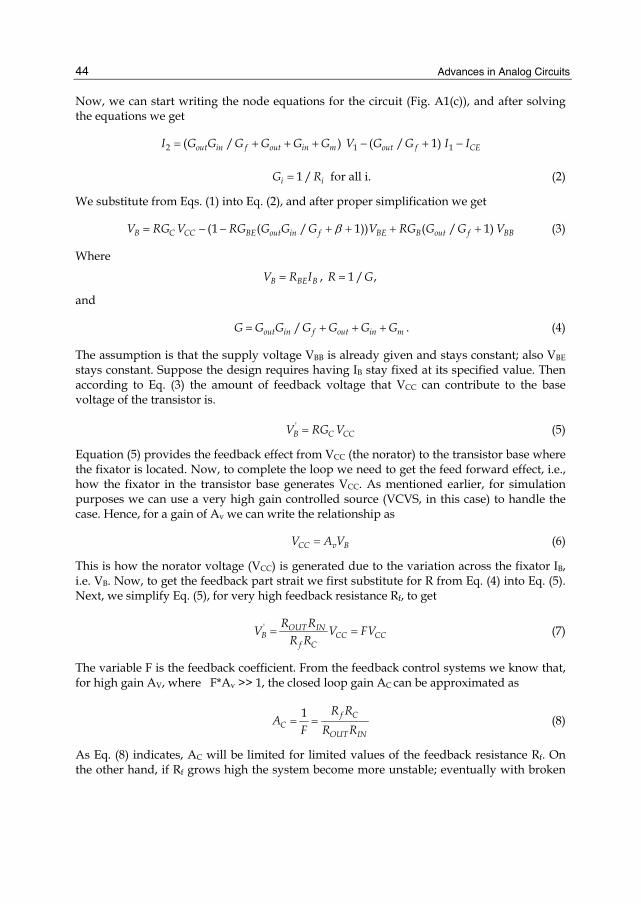
Now, we can start writing the node equations for the circuit (Fig. A1(c)), and after solving the equations we get
2 1 1( / ) ( / 1)out in f out in m out f CEI G G G G G G V G G I I= + + + − + −
1 /i iG R= for all i. (2)
We substitute from Eqs. (1) into Eq. (2), and after proper simplification we get
(1 ( / 1)) ( / 1)B C CC BE out in f BE B out f BBV RG V RG G G G V RG G G Vβ= − − + + + + (3)
Where
,B BE BV R I= 1 / ,R G=
and
/out in f out in mG G G G G G G= + + + . (4)
The assumption is that the supply voltage VBB is already given and stays constant; also VBE stays constant. Suppose the design requires having IB stay fixed at its specified value. Then according to Eq. (3) the amount of feedback voltage that VCC can contribute to the base voltage of the transistor is.
'B C CCV RG V= (5)
Equation (5) provides the feedback effect from VCC (the norator) to the transistor base where the fixator is located. Now, to complete the loop we need to get the feed forward effect, i.e., how the fixator in the transistor base generates VCC. As mentioned earlier, for simulation purposes we can use a very high gain controlled source (VCVS, in this case) to handle the case. Hence, for a gain of Av we can write the relationship as
CC v BV A V= (6)
This is how the norator voltage (VCC) is generated due to the variation across the fixator IB, i.e. VB. Now, to get the feedback part strait we first substitute for R from Eq. (4) into Eq. (5). Next, we simplify Eq. (5), for very high feedback resistance Rf, to get
' OUT INB CC CC
f C
R RV V FVR R
= = (7)
The variable F is the feedback coefficient. From the feedback control systems we know that, for high gain AV, where F*Av >> 1, the closed loop gain AC can be approximated as
1 f CC
OUT IN
R RA
F R R= = (8)
As Eq. (8) indicates, AC will be limited for limited values of the feedback resistance Rf. On the other hand, if Rf grows high the system become more unstable; eventually with broken

A New Approach to Biasing Design of Analog Circuits
45
feedback a fixator fails to generate the required DC supply (VCC) as a substitution for the pairing norator.
8. Acknowledgment The author would like to thank Ms. Golnaz Hashemian for her valuable suggestions and editing the chapter.
9. References [1] A.S. Sedra, and K.C. Smith, Microelectronic Circuit 6th ed. Oxford University Press, 2010. [2] R.C.Jaeger, and T.N. Blalock, Microelectronic Circuit Design 4th ed. Mc Graw-Hill Higher
Education, 2010. [3] C. J. Verhoeven, Arie van Staveren, G. L. E. Monna, M. H. L. Kouwenhoven, E. Yildiz,
Structured Electronic Design: Negative-Feedback Amplifiers, Kluwer Academic Publishers, 2003.
[4] R. Hashemian, “Local Biasing and the Use of Nullator-Norator Pairs in Analog Circuits Designs,” VLSI Design, vol. 2010, Article ID 297083, 12 pages, 2010. doi:10.1155/2010/297083. http://www.hindawi.com/journals/vlsi/2010/297083.html
[5] ___, "Analog Circuit Design with Linearized DC Biasing ", Proceedings of the 2006 IEEE Intern. Conf. on Electro/Information Technology, Michigan State University; Lancing, MI, May 7– 10, 2006.
[6] ___, " Designing Analog Circuits with Reduced Biasing Powe", Proceedings of the 13th IEEE International Conference on Electronics, Circuits and Systems, Nice, France Dec. 10– 13, 2006
[7] R. Kumar, and R. Senani, “Bibliography on Nullor and Their Applications in Circuit Analysis, Synthesis and Design”, Analog Integrated Circuit and Signal Processing, Kluwer Academic Pub, 2002.
[8] H. Schmid, “Approximating the universal active element”, IEEE Trans. on Cir. and Sys. II, Volume 47, Issue 11, Nov 2000, pp 1160 – 1169.
[9] E. Tlelo-Cuautle, M.A. Duarte-Villasenor, C.A. Reyes-Garcia, M. Fakhfakh, M. Loulou, C. Sanchez-Lopez, and G. Reyes-Salgado, “Designing VFs by applying genetic algorithms from nullator-based descriptions”, ECCTD 2007, 18th European Conference on Circuit Theory and Design, Volume, Issue , 27-30 Aug. 2007, pp 555 – 558.
[10] E. Teleo-Cuautle, L.A. Sarmiento-Reyes, “Biasing analog circuits using the nullor concept”, Southwest Symp. on Mixed-Signal Design, 2000.
[11] D.G. Haigh, and P.M. Radmore, “Admittance Matrix Models for the Nullor Using Limit Variables and Their Application to Circuit Design”, IEEE Transactions on Circuits and Systems I: Regular Papers, Volume 53, Issue 10, Oct. 2006, pp 2214 – 2223.
[12] Claudio Beccari "Transmission zeros", Departimento di Electronica, Turin Institute of Technology, Turino, Italy; December 6, 2001.
[13] D.G. Haigh, T.J.W. Clarke, and P.M. Radmore, “Symbolic Framework for Linear Active Circuits Based on Port Equivalence Using Limit Variables”, IEEE Transactions on Circuits and Systems I: Regular Papers, Volume 53, Issue 9, Sept. 2006, pp 2011 – 2024.

Advances in Analog Circuits
46
[14] T.L. Pillage, R.A. Rohrer, C. Visweswariah, Electronic Circuit & System Simulation Methods, McGraw-Hill, Inc., 1995.
[15] J. Vlach and K. Singhal, computer methods for circuit analysis and design, Van Nostrand Reinhold Electrical/Computer Science and Engineering Series, 1983.
[16] L.W. Nagel, "SPICE2, A computer program to simulate semiconductor circuits," Univ. of California, Berkeley, CA, Memorandum no. ERL-M520, 1975.
[17] Mike Smith, "WinSpice3 User’s Manual, v1.05.08", http://www.ousetech.co.uk/winspice2/, May 2006. [18] R. Jacob. Baker, CMOS, Circuit Design, Layout, and Simulation, 2nd ed. IEEE Press, Wiley
Interscience, 2008, pp. 613 – 823. [19] R. Hashemian, “Source Allocation Based on Design Criteria in Analog Circuits”,
Proceedings of the 2010 IEEE International Midwest Symposium On Circuits And Systems, Seattle, WA, August 1 - 4, 2010.