Embed Size (px)
Citation preview

Electronic Instrumentation ENGR-4300 Experiment 7
K.A. Connor, S. Bonner, P. Schoch Revised: 4/10/2009
Rensselaer Polytechnic Institute Troy, New York, USA
-1-
Experiment 7
Digital Logic Devices and the 555-Timer
Purpose: In this experiment we address the concepts of digital electronics and look at the 555-timer, a device that
uses digital devices and other electronic switching elements to generate pulses.
Equipment Required:
• Voltmeter (Rensselaer IOBoard)
• Oscilloscope (Rensselaer IOBoard)
• Function Generator (Rensselaer IOBoard)
• +4V or +5V (+Vcc) Power Supply (Rensselaer IOBoard, on RED2 be sure to use V+ and GND)
• 555-Timer,7402, 7404, 7410, 7414, 74107, 74393 ICs
Helpful links for this experiment can be found on the links page for this course:
http://hibp.ecse.rpi.edu/~connor/education/EILinks.html#Exp7
Part A – Basic Logic Gates
Background
Digital logic gates: All digital logic gates are based on binary logic. Binary logic has two values, called TRUE and
FALSE, LOGIC 1 and LOGIC 0, ON and OFF, or HIGH and LOW. The corresponding binary number can have
two possible values, 1 and 0. Digital logic gates perform many common logic operations on binary signals, such as
AND, OR, NOT, NAND, and NOR. The table in Figure A-1 contains the common symbol for each type of gate, an
expression for the function of the gate in Boolean algebra, and a truth table for the device. The truth table shows
how the gate will behave for all possible combinations of digital inputs.
Figure A-1.

Electronic Instrumentation ENGR-4300 Experiment 7
K.A. Connor, S. Bonner, P. Schoch Revised: 4/10/2009
Rensselaer Polytechnic Institute Troy, New York, USA
-2-
Figure A-1 (continued).
Digital logic chips: In TTL (transistor-transistor logic) digital electronic circuits, the representation of binary
numbers in terms of voltages is about 5V for LOGIC 1 and about 0V for LOGIC 0. About 5V usually means a
voltage between 2 and 5V while about 0V means any voltage in the range 0 to 0.8V. The voltage levels when using
TTL devices must always be in the ranges indicated or the circuits will not function correctly. LOGIC 1 and LOGIC
0 are the only output levels one should see with logical devices. This is one characteristic that makes them differ
from analog devices. They also switch very fast from one state to the other. Switching speeds are usually much
faster than for analog devices, especially cheap devices like the 741 op-amp.
A digital chip generally has 14- or 16-pins. It usually contains more than one of the same logic gate. (For example,
a 14-pin chip will have six single-input gates or four 2-input gates.) By convention, the upper right pin on a digital
chip is always connected to HIGH (+Vcc) and the bottom left pin to LOW (0V). Vcc is usually either +4V or +5V,
depending on what supplies are available. Most logic chips will operate over a range of supply voltages. On a 14-
pin chip this corresponds to pin 7 (0V) and pin 14 (+Vcc) and on a 16-pin chip, pin 8 (0V) and pin 16 (+Vcc).
These two connections provide reference values for the operations the chips perform. Generally circuit diagrams do
not show these two reference connections. If you forget to connect these two pins, your circuit will not function
correctly.
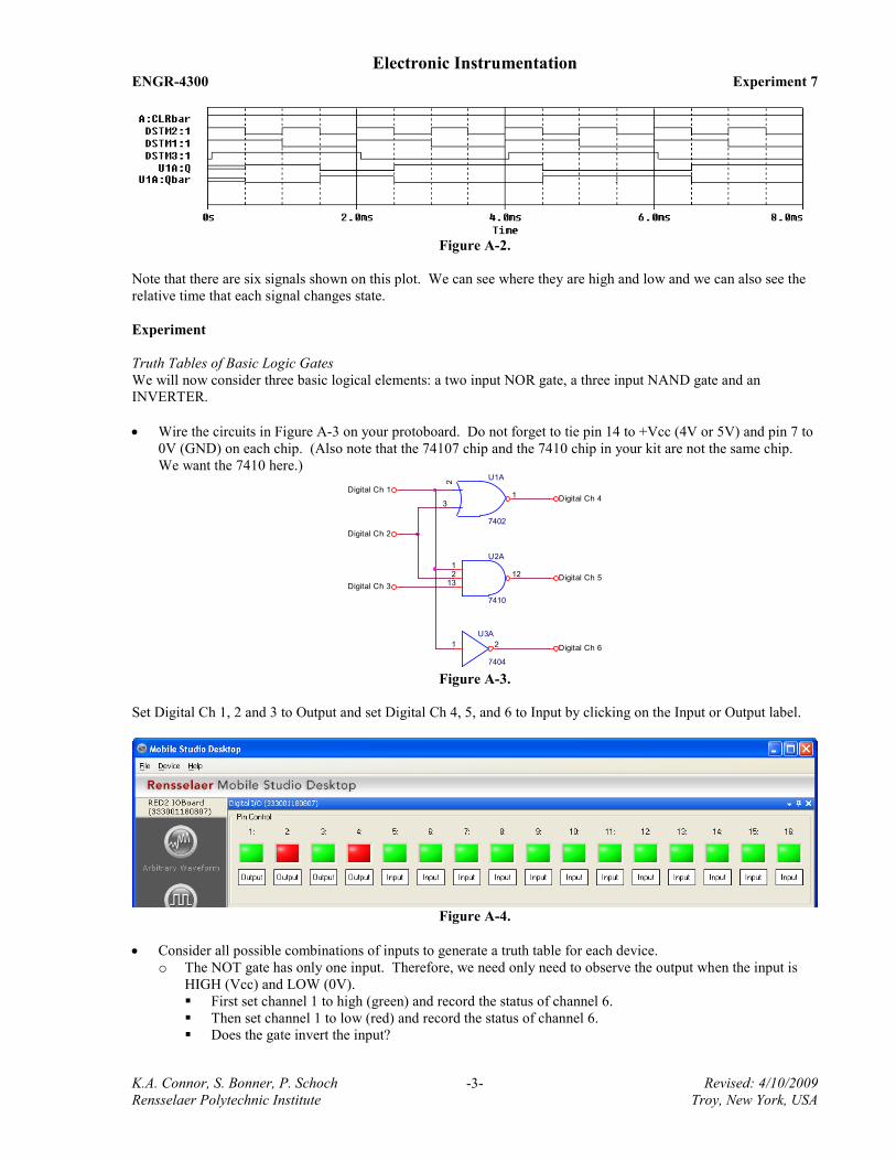
Timing diagrams: Timing diagrams are a special kind of transient output which are useful for viewing many binary
signals. Since the voltage levels of binary signals can only be either high or low, knowing the exact voltage level is
not as significant as knowing when the different signals transition from high to low (or low to high). A timing
diagram is much easier to read when you need to compare many binary signals. Unlike a regular PSpice plot (where
all signals are displayed with the same voltage and time axis) a timing diagram displays the signals on separate lines
with the same time scale. A sample is shown in Figure A-2.
Electronic Instrumentation ENGR-4300 Experiment 7
K.A. Connor, S. Bonner, P. Schoch Revised: 4/10/2009
Rensselaer Polytechnic Institute Troy, New York, USA
-3-
Figure A-2.
Note that there are six signals shown on this plot. We can see where they are high and low and we can also see the
relative time that each signal changes state.
Experiment
Truth Tables of Basic Logic Gates
We will now consider three basic logical elements: a two input NOR gate, a three input NAND gate and an
INVERTER.
• Wire the circuits in Figure A-3 on your protoboard. Do not forget to tie pin 14 to +Vcc (4V or 5V) and pin 7 to
0V (GND) on each chip. (Also note that the 74107 chip and the 7410 chip in your kit are not the same chip.
We want the 7410 here.) U1A
7402
2
31
U2A
7410
1122
13
U3A
7404
1 2
Digital Ch 2
Digital Ch 1
Digital Ch 3
Digital Ch 4
Digital Ch 6
Digital Ch 5
Figure A-3.
Set Digital Ch 1, 2 and 3 to Output and set Digital Ch 4, 5, and 6 to Input by clicking on the Input or Output label.
Figure A-4.
• Consider all possible combinations of inputs to generate a truth table for each device.
o The NOT gate has only one input. Therefore, we need only need to observe the output when the input is
HIGH (Vcc) and LOW (0V).
First set channel 1 to high (green) and record the status of channel 6.
Then set channel 1 to low (red) and record the status of channel 6.
Does the gate invert the input?

Electronic Instrumentation ENGR-4300 Experiment 7
K.A. Connor, S. Bonner, P. Schoch Revised: 4/10/2009
Rensselaer Polytechnic Institute Troy, New York, USA
-4-
Take a picture (screen capture) of one of the input/output combinations.
Draw a truth table for this gate on the output plot. Include this plot in your report.
o Now you will repeat this process for the other two gates.
The NOR gate has two inputs, so we must observe the output at pin 1 (Digital I/O channel 4) for all
possible combinations of binary inputs at pins 2 and 3: (LOW, LOW), (LOW, HIGH), (HIGH, LOW)
and (HIGH, HIGH).
Take a picture (screen capture) of one of the input/output trace combinations.
Record the truth table on the plot. Include this plot in your report.
The NAND gate has three inputs. How many combinations of HIGH and LOW are required to fully
test this gate?
Record the input and output for this gate in a truth table on a sample screen capture, as well. Include
this plot in your report.
Simulation of Basic Logic Gates
We will now wire the same three basic logical elements using PSpice.
• Create the following circuit (Figure A-5) in PSpice.
Figure A-5.
o Wiring the circuit in PSpice is somewhat different than on the protoboard.
PSpice assumes that the +5V and 0V references have already been wired, so you do not need to make
these connections.
We cannot simply move the wires to record all possibilities. Therefore, we use digital clocks with
different pulse lengths to create the signals we need to test the gates.
We have removed the resistors connecting the gate outputs to ground. This tells PSpice to output
timing diagrams by default.
o Now we need to set the clocks up to work with different pulse lengths.
Use DigClock in the SOURCE library
Use the default settings for DSTM1 (no delay, on time = 0.5us, off time = 0.5us).
For DSTM2, double the on and off times to 1us.
For DSTM3, double them again to 2us.
• Run a simulation
o Simulate for 8us with a step size of 0.01us.
o Display all the inputs from the clocks and the output of each of the three gates.
o Produce a hardcopy of the timing diagram with the inputs and the outputs for all three gates.
Mark the output trace for each gate on the diagram. For each gate, generate the truth table for the
device based on the outputs and inputs you observe on the timing diagram. Write them on the output
plot.
Include this plot in your report.
Do your results agree with the truth tables you found using from the circuits you built?

Electronic Instrumentation ENGR-4300 Experiment 7
K.A. Connor, S. Bonner, P. Schoch Revised: 4/10/2009
Rensselaer Polytechnic Institute Troy, New York, USA
-5-
Summary
Basic logic gates allow you to use electronic signals to perform operations on digital signals. They can also be
combined to perform more complex operations, such as addition and subtraction. This makes them a basic building
block of digital computers.
Part B – Flip Flops
Background
Flip Flops: It is possible using basic logic gates to build a circuit that remembers its present condition. These
circuits are called flip flops. The PSpice symbol for a JK flip flop is pictured in Figure B-1. There are several
different kinds of flip flops with slightly different characteristics. In this course we use the JK flip flop. JK flip
flops, like other flip flops have four inputs, two outputs and the usual two power connections (VCC and ground). The
outputs are labeled Q and Q (also called Qbar and NQ). They are complements of one another. Thus, when Q
is LOW, Qbar is HIGH, etc. CLK is the digital clock. A flip flop only changes its output when the clock pulse at
CLK goes from HIGH (+Vcc) to LOW (0V). This is called the “falling edge” of the clock. The input CLR , when
LOW, will reset the outputs to a known state. It has the following truth table:
Figure B-1.
Note that the flip flop is an edge-triggered device. This means that instead of changing state as soon as its inputs
change, it “waits” until it receives a falling edge at the clock input (CLK). To decide how to set the output, the flip
flop “looks” at the values at the inputs at J and K AND at the current value of the output. Based on these three
values, it decides how to reset the output.
You may be familiar with clocks. They are used to coordinate the instructions performed by the CPU and other
devices in a computer. When a computer has a clock speed of 1GHz it can handle 1×10⁹ instructions per second;
one for every clock cycle. The flip flop works on the same principal. With every clock cycle, it looks at its inputs
and changes state accordingly.
The flip flop is a memory device. If both inputs are zero, its output will remain the same indefinitely. A bank of 4
flip flops can store a digital byte of memory in a computer. If you want to change the value of a single bit of that
byte to zero, you can set the inputs to the corresponding flip flop to J = 0 and K = 1. On the next clock cycle, the
output will change to zero. If you want to change a single bit of the byte to one, you can set the inputs of the
corresponding flip flop to J = 1 and K = 0. On the next clock cycle, the output will change to 1. You can also toggle
the value of the flip flop output by setting both inputs to 1.
Timing diagram for a flip flop: To illustrate the behavior of a JK flip flop, we wired the circuit in Figure B-2 in
PSpice and created the timing diagram shown in Figure B-3.

Electronic Instrumentation ENGR-4300 Experiment 7
K.A. Connor, S. Bonner, P. Schoch Revised: 4/10/2009
Rensselaer Polytechnic Institute Troy, New York, USA
-6-
CLK
DSTM4
CLK
DSTM3
CLK
DSTM2
CLK
DSTM1
U1A
74107
1
4
13
3
212
J
K
CLR
Q
QCLK
Figure B-2.
Figure B-3.
DSTM2 is the clock. Each time the clock falls, look at the values of the inputs at J (DSTM1), K (DSTM3), and the
output signal (U1A:Q). If the truth table is correct, what should the output value at U1A:Q be for each
combination? Is the timing diagram correct? Please check the datasheet for the SN74107 flip flop located on the
course web page for details about this device.
Noise and Digital Circuits: Any time you build a circuit, there will be noise. In an edge-triggered device, where
timing is a factor, noise can cause many problems. A noise spike might be interpreted as the falling edge of the
clock. If this happens, the flip flop will change state at the wrong time and possibly with the wrong inputs. To
avoid this problem, it is essential to use a bypass capacitor in every timed digital circuit you build. A bypass
capacitor is simply a capacitor placed between the source voltage and ground. What it does is filter out high
frequency noise, so that any spikes that might be misinterpreted are filtered out. Figure B-4 shows a bypass
capacitor.
Figure B-4.
To understand how the bypass capacitor works, we only need to recall that a capacitor looks like an open circuit at
low frequencies and a short at high frequencies. Digital signals consist of two DC values, 0V and +Vcc. A DC
voltage has zero frequency. Therefore the bypass capacitor will look like an open circuit and all of the DC signal
will pass into the circuit. A noise spike is a very sudden high frequency event. At high frequencies, the capacitor
looks like a short. Therefore, the high frequency event will pass through the capacitor to ground and not continue on
into the circuit.
When a signal changes from low to high (or high to low), the temporary noise of the transition may cause the device
to make the wrong output decision. Since the values of the inputs, as they are changing, are indeterminate, the
output that a flip flop will generate if the inputs are changing is unknown. In PSpice, this unknown state is depicted
by a double red line. If you look at the timing diagram above you will see that both Q and Qbar start out in an
unknown state until the first falling edge of the clock. Also notice that the transitions for J and K take place well
before the falling edge of the clock. We deliberately set up the timing of DSTM1 and DSTM3 so that they do not
change the state of the input at the same time the clock transitions from high to low. If we had, PSpice would
continue to display the double red line, signifying that it cannot properly set the output because it isn’t sure what the
inputs are supposed to be.
V+
GND

Electronic Instrumentation ENGR-4300 Experiment 7
K.A. Connor, S. Bonner, P. Schoch Revised: 4/10/2009
Rensselaer Polytechnic Institute Troy, New York, USA
-7-
Experiment
The JK Flip Flop
In this part of the experiment, we will look at the behavior of a flip flop on your protoboard.
Set up the 74107 JK flip flop on the protoboard.
o Provide 0V at pin 7 of the chip and +Vcc to pin 14.
o Place a 0.1uF by-pass capacitor between 0 and +Vcc.
o Use three Digital I/O channels to create the J, K, and Clock signals. These should be set as outputs
o Use 2 Digital I/O channels to read the Q and Qbar signals. These are set as inputs.
o Set the CLR to zero to be sure that the flip flop begins in a known state. THEN attach it to +Vcc to enable
the function of the chip. (Or use yet another Digital I/O channel as an output and cycle it low and then
high.)
o Run all possible combinations of logic levels for J and K (see below). Each time you change J or K, you
need to cycle the Digital I/O that is the Clock signal. This means to make the changes in J and/or K and
then switch the clock from low to high and then back to low. By monitoring the Q output, you should be
able to complete the table below. It may take a little thought.
o Fill in the following truth table for this device. You will not be able to fill in the table in order. You will
need to skip around depending on the current state (before pulse) of the flip flop.
Q (before pulse) J K Q (after pulse) Qbar (after pulse)
0 0 1
1 0 1
0 1 0
1 1 0
0 0 0
1 0 0
0 1 1
1 1 1
o Take a screen capture of the Digital I/O status for the case when J and K equal to 1. Label each Digital I/O
channel used with J, K, Clock, Q and Qbar. Copy the truth table above for the flip flop onto a print out of
the Digital I/O status screen capture. Include this plot in your report.
Summary
The JK flip flop is an edge-triggered device that uses an external clock to coordinate state changes with other
clocked devices in a circuit. It is capable of holding its output stable, changing its output directly to high or low, or
toggling the output to the opposite of its current value. It can be used as a memory device or as a building block to
create more complex devices, such as counters.
Part C – Counters
Background
Binary Counters: JK flip flops can be connected in a counter configuration as shown in Figure C-1. The output of
each flip flop is used as the input clock to the next flip flop. On all flip flops, J and K are tied high. This means that
they will toggle on each pulse of their clocks. The first flip flop toggles every clock cycle. The second flip flop

Electronic Instrumentation ENGR-4300 Experiment 7
K.A. Connor, S. Bonner, P. Schoch Revised: 4/10/2009
Rensselaer Polytechnic Institute Troy, New York, USA
-8-
toggles every time the output from the first flip flop changes. This causes it to toggle at a rate equal to half of the
clock rate. By the same reasoning, the third flip flop toggles at a rate ¼ of the clock rate.
Figure C-1.
If we attach a bit of a binary number, (b0,b1,b2), to the output of each flip flop (b0 to the first, b1 to the second, and
b2 to the last). We get a pattern out which corresponds to the binary counting shown in Figure C-2 below:
Figure C-2.
The lowest order bit of the binary numbers toggles from 0 to 1: (0-1-0-1-0-1….). The second order bit also toggles
between 1 and 0, but at half the rate: (0-0-1-1-0-0-1-1-….). The third order bit toggles also, but at half the rate of
the previous bit: (0-0-0-0-1-1-1-1-0-0-….). The pattern in the table is the same as the pattern created by the
cascaded set of flip flops. Thus, the counter is counting.
It is not necessary for us to configure several flip flops to create a counting circuit, because this is already done in
many kinds of chips. The SN74393, for example, has two sets of four JK flip flops connected as binary counters.
Light Emitting Diodes: LEDs (light emitting diodes) are very useful when dealing with digital circuits. Because
they have two states, ON and OFF, you can hook them to a binary signal, and use them directly to observe whether
or not the signal is HIGH or LOW. Although there are conventions for the polarity of diodes, many manufacturers
do not seem to follow them. The best way to determine the polarity of a diode is to place it directly between +Vcc
and ground (with a series resistor). If it lights, use it in that direction. If it doesn’t light, try switching the polarity.
If it lights that way, then use that polarity. If it lights in neither polarity, throw it away. It is burnt out.
LEDs are like light bulbs. They burn out after a while. In order to prolong the life (and brightness) of an LED, it is
a good idea to wire it in series with a small resistor (330 ohms is about right). If the LED is not bright enough, you
can replace the resistor with a smaller one.
Experiment
Simulation of a cascaded binary counter
In this part of the experiment, we will use PSpice to create a simulation of two counters cascaded together. This will
allow us to count to numbers greater than 15.
• Simulate the circuit in Figure C-3 in PSpice.

Electronic Instrumentation ENGR-4300 Experiment 7
K.A. Connor, S. Bonner, P. Schoch Revised: 4/10/2009
Rensselaer Polytechnic Institute Troy, New York, USA
-9-
CLK
DSTM1OFFTIME = 0.5uSONTIME = 0.5uSDELAY =STARTVAL = 0OPPVAL = 1
CLK
DSTM2OFFTIME = 45uSONTIME = 0.5uSDELAY = 0.7uSTARTVAL = 0OPPVAL = 1
U1A
74393
A1
QA3
QB4
QC5
QD6
CLR
2
U1B
74393
A13
QA11
QB10
QC9
QD8
CLR
12
VV
VV
VV
V
V VV
Figure C-3.
o DSTM1 is the actual clock for the counter, DigClock in SOURCE library with OFFTIME = ONTIME =
0.5us.
o DSTM2 (also DigClock) is set up so that it first clears the counters, lets them count, and then clears them
again. (OFFTIME = 45us, ONTIME = 0.5us, DELAY = 0.7us)
o If the PSpice models for counters or flip flops are not cleared initially, they will have indeterminate data.
o By connecting the two counters together as shown, the sequence of numbers 2QD, 2QC, 2QB, 2QA, 1QD,
1QC, 1QB, 1QA (IN THAT ORDER) form the binary number. Since the counter is set up to count clock
pulses, it will count up from 0 (at reset) to the number of pulses sequentially.
• Run the simulation.
o Generate the output for this circuit for time 0 to 100us using 1us increments.
o You should display the reset pulse, the input clock at pin 1 of U1A, and all eight of the counter outputs
(QA, QB, QC, QD for both counters, selected in order from most significant to least significant bit).
o Using the timing diagram, verify that the counters are actually counting. You can use the cursor to easily
get your binary number. The binary value is displayed on the left by the y-axis.
o What is the highest number it counts to before it resets? Express this number both as a binary number and
a decimal number. At what time does it reset?
o Write it on the timing diagram for the circuit. How many pulses will the clock have to cycle through
between the time it is reset and when it hits its maximum value of 11111111?
o Include the timing diagram output in your report.
Build a counter circuit
In this part of the experiment, we will build a counter circuit on the protoboard.
• Build the circuit in Figure C-4 on your protoboard.
U2
+3
-2
V+
7V-
4
OUT6
OS11
OS25
U3A
7414
1 2
U4A
74393
A1
QA3
QB4
QC5
QD6
CLR
2
D1
D2
D3
D4
R1 220
R2 220
R3 220
R4 220
R5 1kR6
1k
0
0 0
FUNC1
Use MAX473:
same pins as uA741
V1 5Vdc
0
LEDs
Figure C-4. FUNC1, Function Generator 1, has a maximum output of 1.25V. The op-amp amplifies this by a
factor of 2. The Schmitt trigger inverter cleans up the signal. Don’t forget that the 74LS14 and the 74LS393
both need power and ground.
o Use the function generator for the clock. Set it for a square wave with a frequency of 20Hz. We are using
a fairly low frequency so that we will be able to see the switching with the LEDs. Use the offset feature to
Skip op-amp & connect AWG1 here (RED2)

Electronic Instrumentation ENGR-4300 Experiment 7
K.A. Connor, S. Bonner, P. Schoch Revised: 4/10/2009
Rensselaer Polytechnic Institute Troy, New York, USA
-10-
shift the square wave up such that it cycles between 0V and 4V. With the RED2 IOBoard, setting the offset
to 2V and the peak-peak voltage to 4V will output a signal that DOES NOT need the op-amp shown in
Figure C-4. With older IOBoards the signal generator can only go between 0V and 1.2V with a 0.6V offset.
Use a Maxim MAX473 or MAX474 op-amp to boost the signal by a factor of 2. These MAX chips works
with a single +Vcc power supply and can drive the output to very near the power supply voltages. Be sure
that you use the oscilloscope to check the operation of the function generator.
o Tie pin 7 to ground and pin 14 to +Vcc on both the 74LS14 and the 74LS393 logic chips.
o Place a 0.1uF by-pass capacitor between +Vcc and ground.
o Check your LEDs by connecting one with a 220 Ohm resistor between +Vcc and ground to see which
polarity causes it to light. Place it in the circuit with the correct polarity. Usually the lead on the flattened
side of the case goes to ground.
o If you cannot find 220 ohm resistors, use ones close to 220 ohms.
o Set the CLR to +Vcc to be sure that the counter begins counting at zero. THEN attach it to 0V to enable
the chip to function. Note that this is the opposite of the flip flop. The circle at the input to the clear tells
you whether the CLR signal must be high or low. (Circle Hold high to disable clear & enable counting.
No Circle Hold low to disable clear & enable counting.) If you tie this pin incorrectly, the chip will
continuously reset itself and will not work.
• Once you have the circuit working, observe the output.
o Are they changing at the expected rates? Change the function generator frequency if it helps you determine
the frequencies.
o Place channel 1 of the scope on the clock signal and set the time controls so that it displays 50 clock cycles.
Do not change the time scale as you take your pictures. All four should show 50 clock cycles for
comparison purposes.
o You will need to take four pictures using Mobile Studio. Include them in your report.
• Channel 1 = clock and Channel 2 = QA
• Channel 1 = clock and Channel 2 = QB
• Channel 1 = clock and Channel 2 = QC
• Channel 1 = clock and Channel 2 = QD
o What do you observe about the rates of the different signals with respect to the clock? Can you tell which
output corresponds to which bit in the binary number?
o Keep this circuit for part D.
Part D – The 555-Timer
Background
The 555-Timer: The 555-timer is a chip that allows us to create a variety of useful digital and analog signals. Much
like the op-amp, it can be used to perform different functions depending upon what circuit you place it into. The
555-timer can be used to generate digital pulses. When it is wired as a “one-shot” (also called mono-stable mode), it
generates a single, clean, digital pulse at the output, when it experiences a (possibly noisy) pulse at the input. This is
useful when de-bouncing a mechanical switch. In this experiment, we are concerned with the 555-timer when it is
wired in astable mode. This is also called an astable multivibrator. In this mode, the 555-timer circuit creates a
stream of regular pulses. The wiring diagram for the 555-timer in astable mode is shown in Figure D-1.
Electronic Instrumentation ENGR-4300 Experiment 7
K.A. Connor, S. Bonner, P. Schoch Revised: 4/10/2009
Rensselaer Polytechnic Institute Troy, New York, USA
-11-
Figure D-1.
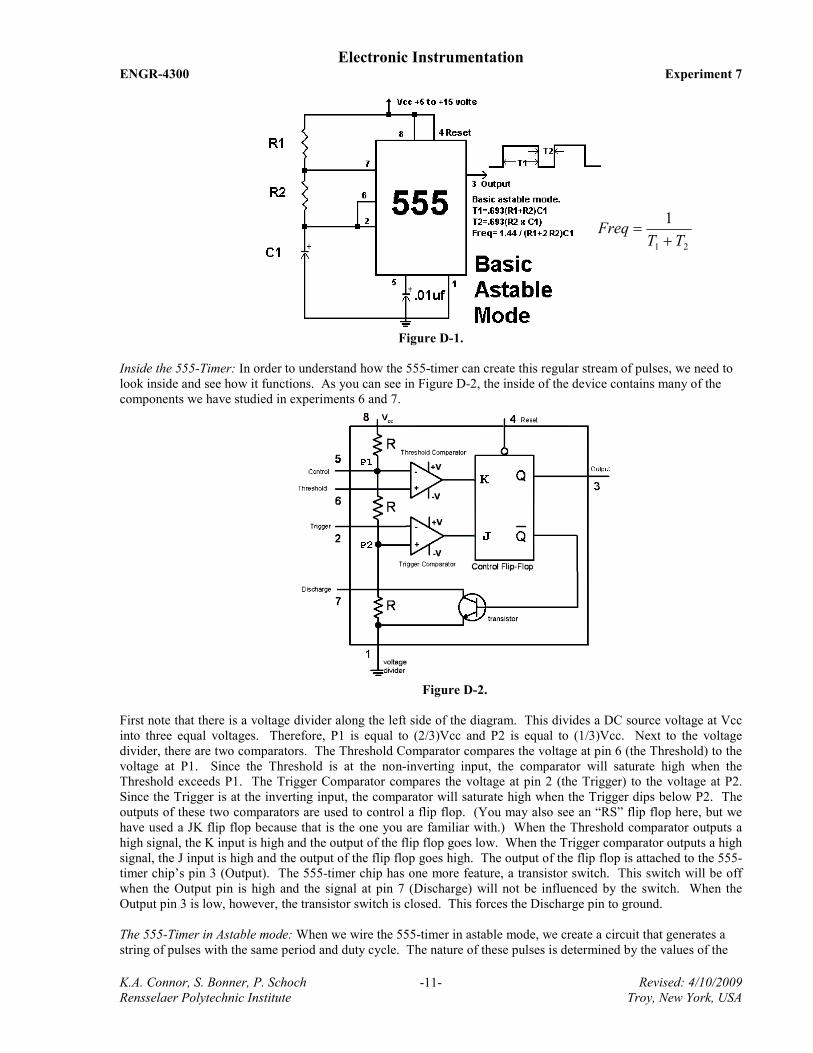
Inside the 555-Timer: In order to understand how the 555-timer can create this regular stream of pulses, we need to
look inside and see how it functions. As you can see in Figure D-2, the inside of the device contains many of the
components we have studied in experiments 6 and 7.
Figure D-2.
First note that there is a voltage divider along the left side of the diagram. This divides a DC source voltage at Vcc
into three equal voltages. Therefore, P1 is equal to (2/3)Vcc and P2 is equal to (1/3)Vcc. Next to the voltage
divider, there are two comparators. The Threshold Comparator compares the voltage at pin 6 (the Threshold) to the
voltage at P1. Since the Threshold is at the non-inverting input, the comparator will saturate high when the
Threshold exceeds P1. The Trigger Comparator compares the voltage at pin 2 (the Trigger) to the voltage at P2.
Since the Trigger is at the inverting input, the comparator will saturate high when the Trigger dips below P2. The
outputs of these two comparators are used to control a flip flop. (You may also see an “RS” flip flop here, but we
have used a JK flip flop because that is the one you are familiar with.) When the Threshold comparator outputs a
high signal, the K input is high and the output of the flip flop goes low. When the Trigger comparator outputs a high
signal, the J input is high and the output of the flip flop goes high. The output of the flip flop is attached to the 555-
timer chip’s pin 3 (Output). The 555-timer chip has one more feature, a transistor switch. This switch will be off
when the Output pin is high and the signal at pin 7 (Discharge) will not be influenced by the switch. When the
Output pin 3 is low, however, the transistor switch is closed. This forces the Discharge pin to ground.
The 555-Timer in Astable mode: When we wire the 555-timer in astable mode, we create a circuit that generates a
string of pulses with the same period and duty cycle. The nature of these pulses is determined by the values of the
21
1
TTFreq
+=

Electronic Instrumentation ENGR-4300 Experiment 7
K.A. Connor, S. Bonner, P. Schoch Revised: 4/10/2009
Rensselaer Polytechnic Institute Troy, New York, USA
-12-
R1-R2-C1 combination on the outside of the timer in the diagram for Basic Astable Mode on the previous page. We
have seen that when current flows through a series combination of a resistor R and a capacitor C, that the circuit
responds with a characteristic time constant τ = RC. The on-time for each pulse is determined by how fast the
capacitor C1 charges when the transistor switch is open and the output of the timer chip at pin 3 is high. In this case,
the capacitor is attached to the source voltage through the resistors R1 and R2. The charging time constant is
τcharge = C1(R1+R2). When the capacitor has charged up to (2/3)Vcc, the Threshold Comparator saturates high, the
flip flop switches, the output goes low and the transistor switch closes. The off-time for each pulse is determined by
how fast the capacitor discharges to ground through the transistor. The discharge path is through R2 to pin 7 to
ground, so the discharging rate is τdischarge = C1(R2). When the capacitor has discharged down to (1/3)Vcc, the
Trigger Comparator saturates high, the flip flop switches, the output goes high, the transistor opens, and the
capacitor is no longer attached to ground at pin 7. The capacitor begins to charge again and the cycle repeats.
By selecting just the right values for the resistors and capacitors in this circuit, we can make the voltage at pin 3 (the
OUTPUT) go from zero to VCC at whatever rate we desire. We can also control the percentage of time that the
output will be on relative to the length of an entire cycle. The equations that govern this behavior are:
1)221(
44.111)2(693.01)21(693.0
CRRTTfCRTCRRT
OFFON
OFFON+
=+
==+=
Pulse width modulation: One of the most important things we can use 555-timers for is to control and drive a large
variety of systems with pulse width modulation. Please read over the links on motor control and flow valve control
on the course links page. The power of pulse width modulation comes from its simplicity. Rather than controlling
the flow of some liquid by carefully opening a valve part way, you can alternately open and close the valve fully in
such a manner that the average open time produces the same effect as a partially open valve. In effect, the rate of
flow is controlled by the duty cycle of the controlling voltage. It is much easier to fully open or close a valve than to
precisely open it part way. One can also apply power to a motor in this manner to control the speed of rotation. The
key goal of this modulation process is to achieve a desired average value for some process. The range of
possibilities is shown in Figure D-3 where A has a high duty cycle (fast) and C a low duty cycle (slow).
Figure D-3.
Experiment
Simulation of a 555-timer circuit
In this part of the experiment, we will use PSpice to demonstrate the operation of the 555-timer chip in astable
mode.

Electronic Instrumentation ENGR-4300 Experiment 7
K.A. Connor, S. Bonner, P. Schoch Revised: 4/10/2009
Rensselaer Polytechnic Institute Troy, New York, USA
-13-
• Wire the circuit in Figure D-4 in PSpice.
Figure D-4.
• Run the simulation.
o Perform a transient analysis in increments of 2us up to 5ms.
o Plot the threshold/trigger, discharge and output voltages. The trigger voltage is pin 2 and the threshold
voltage is pin 6. (They are tied together.) The discharge voltage is pin 7, and the output is taken at pin 3.
o Print your plot and include it in your report.
o Verify that the timer output changes according to the rules listed for the 555-timer in astable mode. Use the
plot to find the time period that the output is ON and the time period that the output is OFF. Note: Do not
use the first cycle of pulses produced by the timer circuit. It takes one cycle to settle in to its steady-state
condition. One of these times should be equal to 0.693(R1+R2)C1 while the other should be equal to
0.693(R2)C1. Which is which? What is the total period of this output?
o Which of the three signals on your plot corresponds to the charging and discharging of the capacitor, C1?
To what voltage does it charge each time? To what voltage does it discharge? What it the rate of charge?
Is the rate of discharge the same?
• Determine the average voltage of the signal.
o Change the end time for the transient analysis to 60ms.
o Display only the output voltage (pin 3) on your plot.
o Rerun the simulation.
o Add a trace of the average of the output using the average function, AVG(). This should add a trace of the
time average of the output voltage. The average at any instant of time is the average of the voltage from
time = 0 to the time of interest. Thus, you should see that the average asymptotically approaches a
particular value.
o Print this plot and write the approximate voltage the average is approaching on the plot.
o Include this plot in your report.
• Find a larger and smaller average voltage for your circuit
o Find an expression for the duty cycle of an astable 555-timer circuit using the equations given. Consider
what relative values of R1 and R2 would produce the highest duty cycle and what relative values of R1 and
R2 would produce the smallest duty cycle.
o Now, using any combination for 3kΩ, 10kΩ or 30kΩ resistors (only one of each value) for R1 and R2, find
the combination of two resistors which results in the largest average voltage and the combination of two
resistors which results in the smallest average voltage.
o Print your plot for each of these two cases, write the values for R1 and R2 you used on each plot. Include
these two plots in your report.

Electronic Instrumentation ENGR-4300 Experiment 7
K.A. Connor, S. Bonner, P. Schoch Revised: 4/10/2009
Rensselaer Polytechnic Institute Troy, New York, USA
-14-
o Verify in each case that the pulses produced by the multivibrator circuit obey the design rules. If the
simulation does not work, the design rules are probably violated.
Build the 555-timer circuit on your protoboard
In this part of the experiment, we will build the astable multivibrator and use it as the clock for your timer circuit.
• Wire the astable multivibrator shown in Figure D-5 on your protoboard.
Figure D-5.
• Record your results.
o You will not be able to see the LED flash because the period of your circuit is too fast.
o Take a Mobile Studio picture of your output.
o Print this plot and include it in your report.
o What is the period of your output signal? What are the off-time and on-time? Use the equations to
calculate what these values should be. How do they compare?
• Slow down the pulses so that you can observe them with the LED.
o Keeping the resistors R1 and R2 the same, determine a new value for C1 such that the period of the timer
will be around 1 second.
o Replace C1 in your circuit and observe the LED. Does it flash once a second?
o What is your on-time and off-time now? How are these related to the on- and off-times of the original
circuit? Why does this relationship hold?
• Use the 555-timer circuit as the clock for your counter.
o Remove the function generator from pin 1 of the counter.
o Connect the output at pin 3 of the 555-timer circuit to pin 1 of your counter circuit.
o Does the counter count the 555-timer pulses?
o Can you see the lower order bits change now?
Report and Conclusions
The following should be included in your written report. Everything should be clearly labeled and easy to find.
Partial credit will be deducted for poor labeling or unclear presentation.
Part A (12 points)
Include the following plots:
1. Mobile Studio plot of a single trace from a NOR gate with truth table. (2 pt)
2. Mobile Studio plot of a single trace from a NAND gate with truth table. (2 pt)
+Vcc

Electronic Instrumentation ENGR-4300 Experiment 7
K.A. Connor, S. Bonner, P. Schoch Revised: 4/10/2009
Rensselaer Polytechnic Institute Troy, New York, USA
-15-
3. Mobile Studio plot of a single trace from a NOT gate with truth table. (2 pt)
4. PSpice timing diagram for the three gates in the circuit with output traces marked. (2 pt)
Answer the following questions:
1. What are the actual voltage values you observed as HIGH and LOW states in the hardware realization of
the circuit? (2 pt)
2. How do the truth tables generated using the actual chips correspond to the truth tables you generated using
your PSpice output? (1 pt)
3. If you had a gate with four inputs, how many cases would you have to consider to create its truth table? (1
pt)
Part B (10 points)
Include the following plot:
1. Mobile Studio plot of a single trace from the flip flop with truth table. (2 pt)
Answer the following questions:
1. Flip flops are called memory devices. Why do you think this is true? (2 pt)
2. Show that the flip flop is giving the correct output at the clock cycles (A ,B, C and D) indicated on the
timing diagram in Figure S-1. DSTM2 is the clock signal, DSTM1 is J, and DSTM3 is K. Show how the
truth table you found for the actual flip flop is consistent with the timing diagram at those four points.
(6 pt)
Figure S-1.
Part C (14 points)
Include the following plots:
1. PSpice timing diagram of counters. (2 pt)
2. Mobile Studio plot of clock and QA. (2 pt)
3. Mobile Studio plot of clock and QB. (2 pt)
4. Mobile Studio plot of clock and QC. (2 pt)
5. Mobile Studio plot of clock and QD. (2 pt)
Answer the following questions:
1. For the counter circuit configuration just studied, what is the highest number it counts to in the time shown
on your output? Express as both a binary and decimal number. (2 pt)
2. How many pulses will the clock have to cycle through after it resets before the counter hits its maximum
value? (1 pt)
3. Which output of the timer (QA, QB, QC, QD) correspond to the bits in the binary number (b3 b2 b1 b0):
N = b3×23 + b2×2
2 + b1×2
1 + b0×2
0. (1 pt)
Part D (36 points)
Include following plots:
1. PSpice plot for the astable circuit with R1 = 10k and R2 = 10k. (2 pt)
2. PSpice plots for the average voltage of the astable circuit with R1 = R2 = 10k. (1 pt)

Electronic Instrumentation ENGR-4300 Experiment 7
K.A. Connor, S. Bonner, P. Schoch Revised: 4/10/2009
Rensselaer Polytechnic Institute Troy, New York, USA
-16-
3. PSpice plot for the average voltage of the astable circuit with highest duty cycle. (1 pt)
4. PSpice plot for the average voltage of the astable circuit with lowest duty cycle. (1 pt)
5. Mobile Studio plot of output from 555-timer circuit when R1 = 1.8k, R2 = 6.8k and C1 = 0.1µF. (4 pt)
Answer following questions:
1. What are the on-time, the off-time, and the period of the signal in plot 1.? What are the calculated values
for these? Are they consistent? (4 pt)
2. What are the maximum and minimum values for the voltage across the capacitor C1 (at pins 2 and 6)?
(Ignore the voltage at times before it reaches steady state.) Why do these values make sense? (3 pt)
3. Calculate the value of τ (the decay constant) that controls the rate at which the capacitor C1 charges.
Calculate the value of τ (the decay constant) that controls the rate at which the capacitor C1 discharges.
(4 pt)
4. What is the minimum duty cycle that can be obtained from the astable multivibrator we modeled using
PSpice? Can you show this mathematically using Duty Cycle = T1/(T1+T2)? (3 pt)
5. What was the average voltage for your original circuit? What were the minimum and maximum average
voltages when you considered different combinations of R1 and R2? (3 pt)
6. What are the on-time, the off-time, and the period of the signal in plot 5.? What are the calculated values
for these? Are they consistent? (4 pt)
7. How did you find the value for C1 that gave the circuit you built a one second period? What value did you
find? (2 pt)
8. What are the calculated on-time, off-time and period values for your circuit with the new capacitor? How
do these relate to the initial values? Why? (4 pt)
Organization and responsibilities (8 points)
1. Discuss mistakes and problems. (6 pt)
2. List member responsibilities. (2 pt)
Total: 80 points for write up +20 for attendance = 100 points
Attendance: 3 classes (20 points), 2 classes (10 points), 1 class (0 points), out of 20 possible points.
Minus 5 points for each late.
No attendance at all = No grade for experiment.