Embed Size (px)
Citation preview
8/11/2019 PART 10-Elec Buk(Final)
http://slidepdf.com/reader/full/part-10-elec-bukfinal 1/21
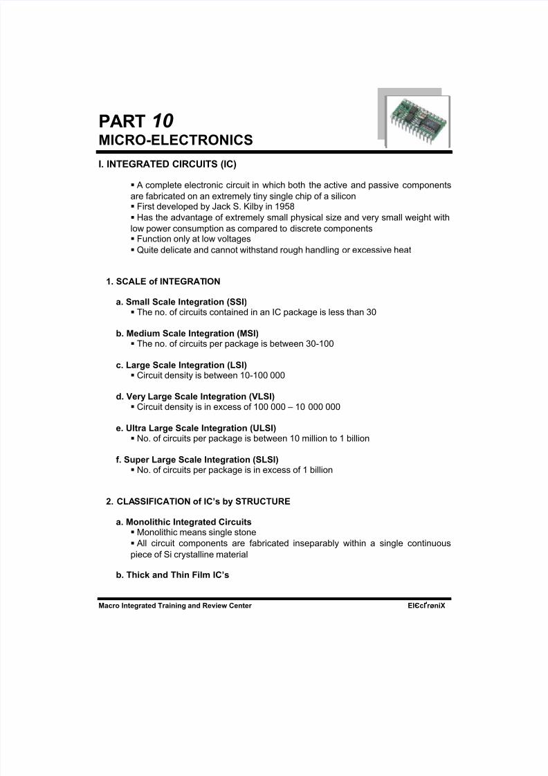
PART 10
MICRO-ELECTRONICSI. INTEGRATED CIRCUITS (IC)
A complete electronic circuit in which both the active and passive componentsare fabricated on an extremely tiny single chip of a silicon
First developed by Jack S. Kilby in 1 !"#as the advantage of extremely small physical si$e and very small weight with
low power consumption as compared to discrete componentsFunction only at low voltages%uite delicate and cannot withstand rough handling or excessive heat
1. SCALE of INTEGRATION
a. Small Scale Integ at!on (SSI)&he no. of circuits contained in an '( package is less than )*
". Me#!$m Scale Integ at!on (MSI)&he no. of circuits per package is between )*+1**
c. La ge Scale Integ at!on (LSI)(ircuit density is between 1*+1** ***
#. %e & La ge Scale Integ at!on (%LSI)
(ircuit density is in excess of 1** *** , 1* *** ***
e. Ult a La ge Scale Integ at!on (ULSI)-o. of circuits per package is between 1* million to 1 billion
f. S$'e La ge Scale Integ at!on (SLSI)-o. of circuits per package is in excess of 1 billion
. CLASSI ICATION of IC*+ "& STRUCTURE
a. Monol!t,!c Integ ate# C! c$!t+onolithic means single stone
All circuit components are fabricated inseparably within a single continuouspiece of Si crystalline material
". T,!c an# T,!n !lm IC*+
Mac o Integ ate# T a!n!ng an# Re !e/ Cente El0c 2n!3
/ry(ell
8/11/2019 PART 10-Elec Buk(Final)
http://slidepdf.com/reader/full/part-10-elec-bukfinal 2/21
14- Micro-Electronics
0nly passive components are formed through the thick and thin filmtechni ues on the insulating surface Active elements are added externally
Thin Film IC’s2esistors and conductors are formed by varying the width and thickness of the
film and by using materials of different resistivity(apacitors are produced by sandwiching an insulating oxide film between two
conducting filmsSmall inductors can be made by depositing a spiral formation of film
Thick Film IC’s3rinted thin film circuitsSilk screen printing techni ues are employed to create the desired circuit
pattern on the surface of a substrate
c. 5&" !# o M$lt!c,!' IC*+ Are formed by either interconnecting a number of individual chips or bycombination of thin film or monolithic '( techni ues
6. CLASSI ICATION of IC*+ "& UNCTIONS
a. L!nea IC*+ Analog '(4s Applications include op+amps5 power5 microwave amplifier5 voltage
comparators5 multiplexers5 voltage regulators6
". D!g!tal IC*+7sed in switching circuitsonolithic integration
Some applications includes logic gates5 flip flops5 counters5 clock chips5calculator chips5 memory chips and microprocessors
7. MONOLIT5IC IC*+ PREPARATION
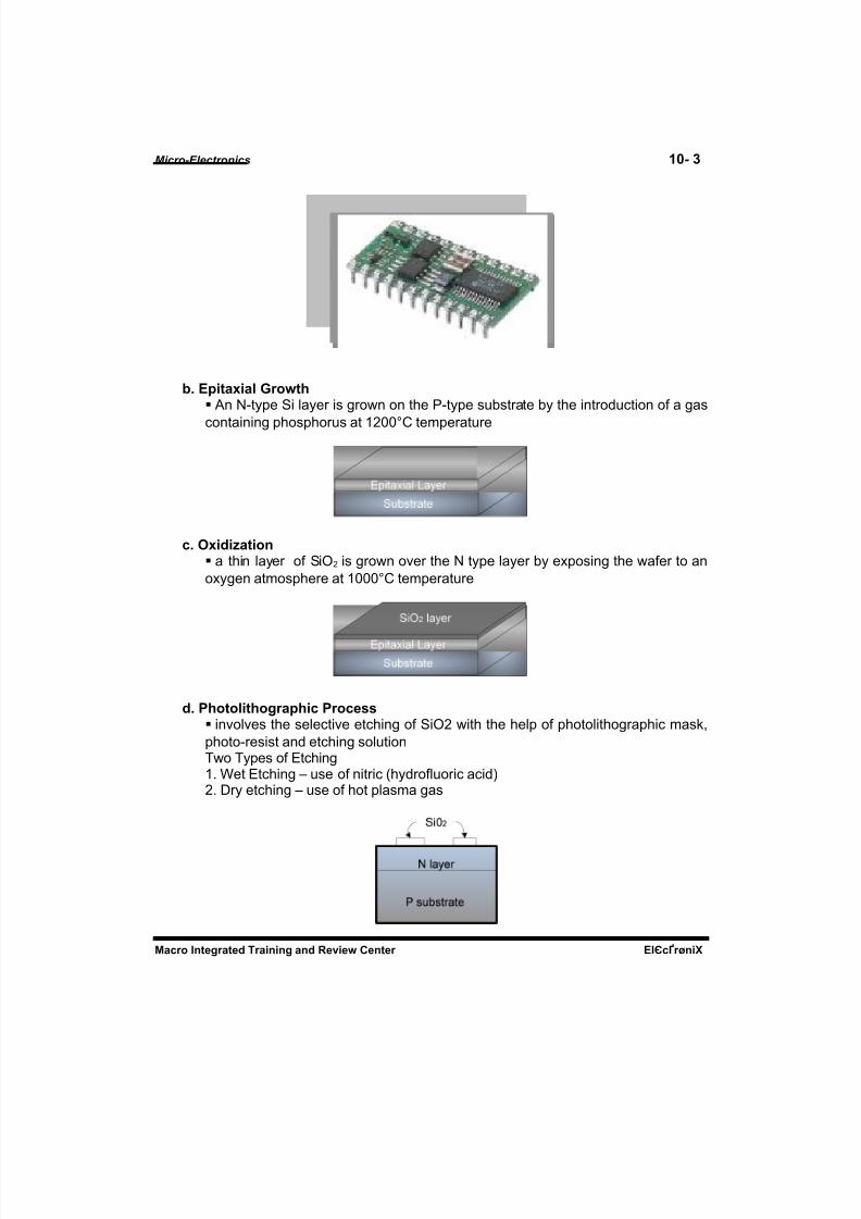
a. 8afe P e'a at!on A 3+type Si bar 8ingot9 is taken and cut into thin slices called wafersC9oc, al+ ! Met,o# is one of the most popular process in ingot growth
:afers are thin sliced of a semiconductor material either circular or rectangular in shape in which a number of '(4s are fabricated simultaneously
&hese wafers are being tapped and polished to mirror finish and serve as thesubstrate for hundred of '(4s
El0c 2n!3 Mac o Integ ate# T a!n!ng an# Re !e/ Cente
8/11/2019 PART 10-Elec Buk(Final)
http://slidepdf.com/reader/full/part-10-elec-bukfinal 3/21
8/11/2019 PART 10-Elec Buk(Final)
http://slidepdf.com/reader/full/part-10-elec-bukfinal 4/21
14-7 Micro-Electronics
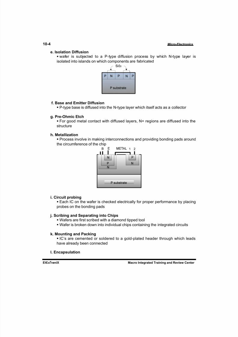
e. I+olat!on D!ff$+!onwafer is sub>ected to a 3+type diffusion process by which -+type layer is
isolated into islands on which components are fabricated
f. ;a+e an# Em!tte D!ff$+!on3+type base is diffused into the -+type layer which itself acts as a collector
g. P e-O,m!c Etc,For good metal contact with diffused layers5 -? regions are diffused into thestructure
,. Metall!9at!on3rocess involve in making interconnections and providing bonding pads around
the circumference of the chip
!. C! c$!t ' o"!ng=ach '( on the wafer is checked electrically for proper performance by placing
probes on the bonding pads
<. Sc !"!ng an# Se'a at!ng !nto C,!'+:afers are first scribed with a diamond tipped tool:afer is broken down into individual chips containing the integrated circuits
. Mo$nt!ng an# Pac !ng'(4s are cemented or soldered to a gold+plated header through which leads
have already been connected
l. Enca'+$lat!on
El0c 2n!3 Mac o Integ ate# T a!n!ng an# Re !e/ Cente
8/11/2019 PART 10-Elec Buk(Final)
http://slidepdf.com/reader/full/part-10-elec-bukfinal 5/21
8/11/2019 PART 10-Elec Buk(Final)
http://slidepdf.com/reader/full/part-10-elec-bukfinal 6/21
14-> Micro-Electronics
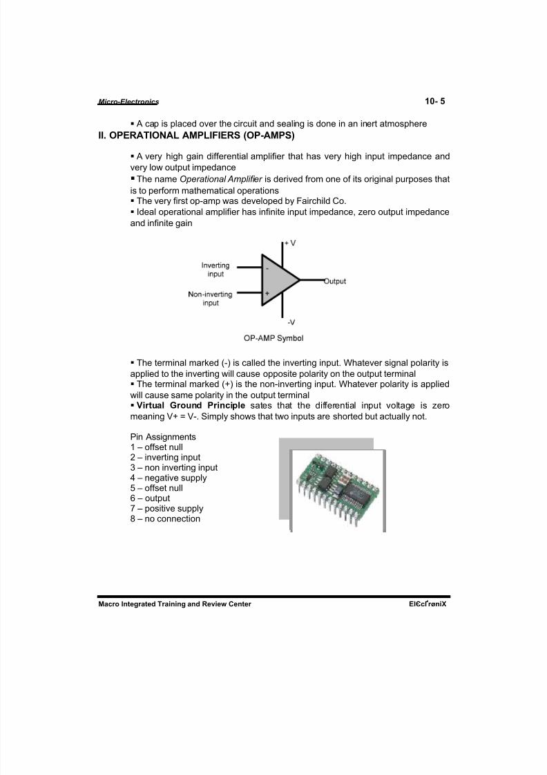
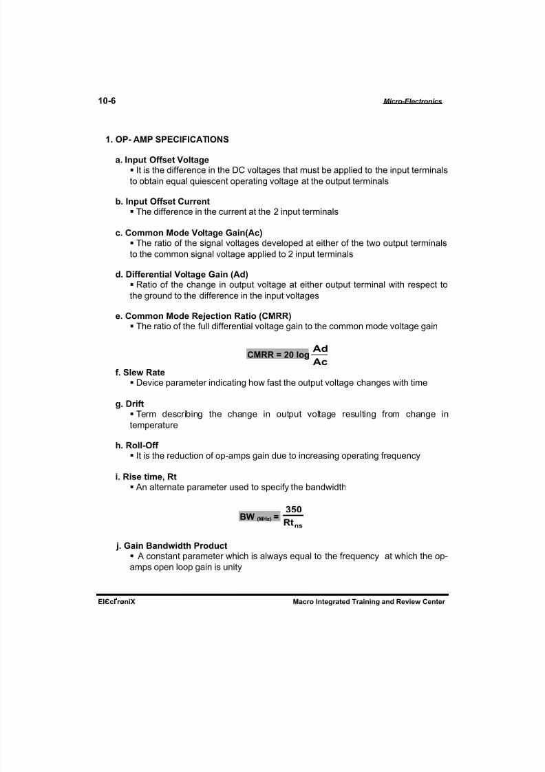
1. OP- AMP SPECI ICATIONS
a. In'$t Off+et %oltage't is the difference in the /( voltages that must be applied to the input terminals
to obtain e ual uiescent operating voltage at the output terminals
". In'$t Off+et C$ ent&he difference in the current at the ; input terminals
c. Common Mo#e %oltage Ga!n(Ac)&he ratio of the signal voltages developed at either of the two output terminals
to the common signal voltage applied to ; input terminals
#. D!ffe ent!al %oltage Ga!n (A#)2atio of the change in output voltage at either output terminal with respect to
the ground to the difference in the input voltages
e. Common Mo#e Re<ect!on Rat!o (CMRR)&he ratio of the full differential voltage gain to the common mode voltage gain
CMRR ? 4 logAc
A#
f. Sle/ Rate/evice parameter indicating how fast the output voltage changes with time
g. D !ft&erm describing the change in output voltage resulting from change intemperature
,. Roll-Off 't is the reduction of op+amps gain due to increasing operating fre uency
!. R!+e t!me@ Rt An alternate parameter used to specify the bandwidth
;8 (M59) ?n+Rt
6=4
<. Ga!n ;an#/!#t, P o#$ct A constant parameter which is always e ual to the fre uency at which the op+
amps open loop gain is unity
El0c 2n!3 Mac o Integ ate# T a!n!ng an# Re !e/ Cente
8/11/2019 PART 10-Elec Buk(Final)
http://slidepdf.com/reader/full/part-10-elec-bukfinal 7/21
Micro-Electronics 14-
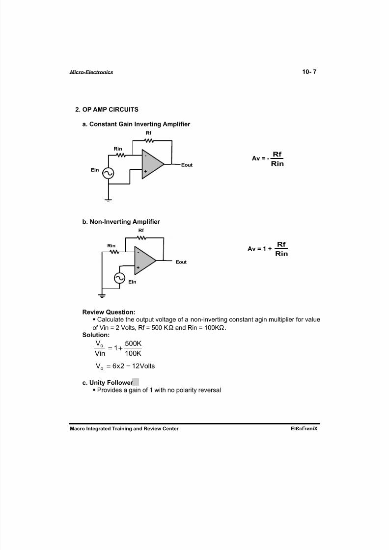
. OP AMP CIRCUITS
a. Con+tant Ga!n In e t!ng Am'l!f!e
A ? -R!n
Rf
". Non-In e t!ng Am'l!f!e
A ? 1 BR!n
Rf
Re !e/ $e+t!on(alculate the output voltage of a non+inverting constant agin multiplier for value
of @in ; @olts5 2f !** K Ω and 2in 1**K Ω.
Sol$t!on
K1**K!**
1@in@o +=
@olts1;;xC@o ==
c. Un!t& ollo/e3rovides a gain of 1 with no polarity reversal
Mac o Integ ate# T a!n!ng an# Re !e/ Cente El0c 2n!3
B
-
E!nEo$t
Rf
R!n
B
-
E!n
Eo$t
Rf
R!n
8/11/2019 PART 10-Elec Buk(Final)
http://slidepdf.com/reader/full/part-10-elec-bukfinal 8/21
14- Micro-Electronics
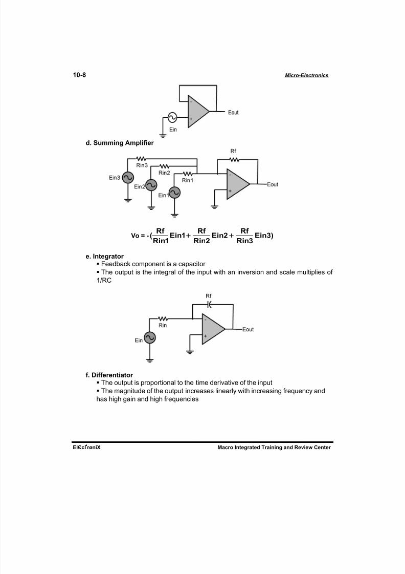
#. S$mm!ng Am'l!f!e
%o ? - )6E!n6R!n
Rf E!n
R!nRf
1E!n1R!n
Rf (
e. Integ ato Feedback component is a capacitor &he output is the integral of the input with an inversion and scale multiplies of
1E2(
f. D!ffe ent!ato &he output is proportional to the time derivative of the input&he magnitude of the output increases linearly with increasing fre uency and
has high gain and high fre uencies
El0c 2n!3 Mac o Integ ate# T a!n!ng an# Re !e/ Cente
8/11/2019 PART 10-Elec Buk(Final)
http://slidepdf.com/reader/full/part-10-elec-bukfinal 9/21
Micro-Electronics 14- F
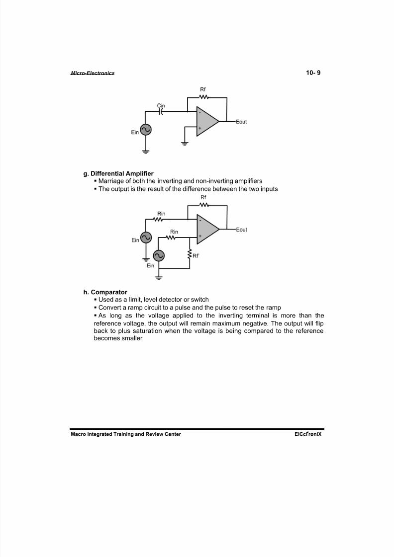
g. D!ffe ent!al Am'l!f!e
arriage of both the inverting and non+inverting amplifiers&he output is the result of the difference between the two inputs
,. Com'a ato 7sed as a limit5 level detector or switch(onvert a ramp circuit to a pulse and the pulse to reset the ramp
As long as the voltage applied to the inverting terminal is more than thereference voltage5 the output will remain maximum negative. &he output will flipback to plus saturation when the voltage is being compared to the referencebecomes smaller
Mac o Integ ate# T a!n!ng an# Re !e/ Cente El0c 2n!3
8/11/2019 PART 10-Elec Buk(Final)
http://slidepdf.com/reader/full/part-10-elec-bukfinal 10/21
14-14 Micro-Electronics
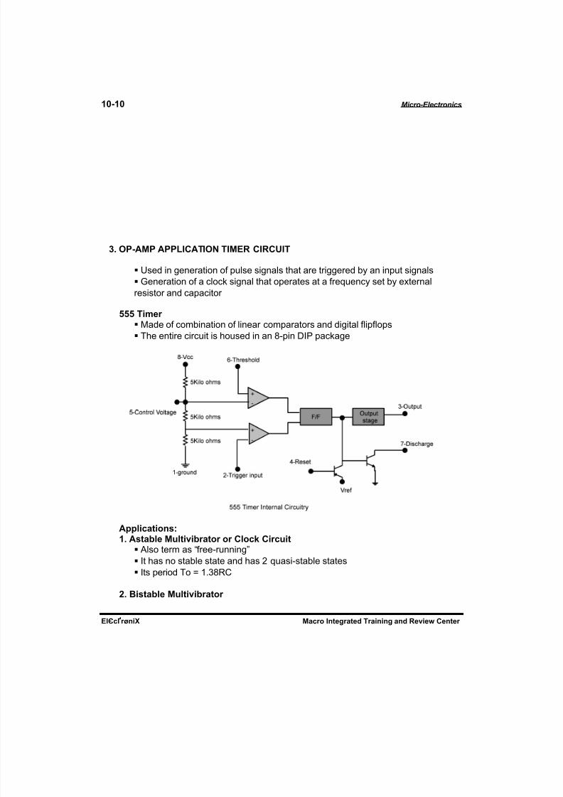
6. OP-AMP APPLICATION TIMER CIRCUIT
7sed in generation of pulse signals that are triggered by an input signalseneration of a clock signal that operates at a fre uency set by external
resistor and capacitor
=== T!me ade of combination of linear comparators and digital flipflops
&he entire circuit is housed in an "+pin /'3 package
A''l!cat!on+ 1. A+ta"le M$lt! !" ato o Cloc C! c$!t
Also term as Gfree+runningH't has no stable state and has ; uasi+stable states'ts period &o 1.)"2(
. ;!+ta"le M$lt! !" ato
El0c 2n!3 Mac o Integ ate# T a!n!ng an# Re !e/ Cente
8/11/2019 PART 10-Elec Buk(Final)
http://slidepdf.com/reader/full/part-10-elec-bukfinal 11/21
Micro-Electronics 14- 11
Iasically the Flipflop
=ccles Jordan (ircuit#as two stable states and no uasi+stable state
6. Mono-Sta"le M$lt! !" ato 0ne shot#as one stable state and 1 uasi+stable state'ts period &o *.C 2(
TEST OURSEL 10
Re !e/ $e+t!on+ 1. 't is a layer of photosensitive material that is first coated in a wafer during photolithographicprocess.
a. maskb. photoresistc. photomateriald. silicon dioxide
An+/e b. photoresist
;. 't is a combination of film and monolithic '( techni ues that is being applied to variety of multichip integrated circuits.
a. mixtureb. hybridc. combinedd. fusion
An+/e b. hybrid
). &hick film employs silk screen techni ues in the formation of passive components5 what is thenthe process involve for thin film circuits for the same purpose
a. cathode sputtering techni ueb. anode sputtering techni uec. isolation diffusiond. metalli$ation
An+/e a. cathode sputtering techni ue
B. 'n '( production5 it is the introduction of controlled small uantities of a material into the crystalstructure for modification of its electrical characteristicsa. =tchingb. /opingc. =pitaxial growthd. /iffusion
Mac o Integ ate# T a!n!ng an# Re !e/ Cente El0c 2n!3
8/11/2019 PART 10-Elec Buk(Final)
http://slidepdf.com/reader/full/part-10-elec-bukfinal 12/21
14-1 Micro-Electronics
An+/e d. /iffusion
!. :hat is the process that is being defined when the metal is bombarded by high velocity inert gasatoms causing some atoms of the metal to be dislodge
a. evaporationb. bombardmentc. sputteringd. diffusion
An+/e c. sputtering
C. An integrated circuit op+amps has .a. two inputs and two outputsb. two inputs and one outputc. one input and two outputsd. multiple inputs and one output
An+/e b. two inputs and one output
D. 'n the differential mode5a. opposite polarity signals are applied to the inputsb. the gain is 1c. the outputs are differential amplitudesd. only one supply voltage is used
An+/e a. opposite polarity signals are applied to the inputs
". &he output of a particular op+amp increases "@ in 1;Ls. &he slew rate is .a. C @E Lsb. *.CD @E Lsc. 1.! @E Lsd. C @+ Ls
An+/e b. *.CD @E LsSol$t!on
Slew 2ate sLE@CD.*1;"
. &he purpose of offset nulling on operational amplifier is to .a. reduce the gainb. e uali$e the input signal
c. $ero the output error voltaged. both b and c
An+/e c. $ero the output error voltage
1*. A voltage follower .
El0c 2n!3 Mac o Integ ate# T a!n!ng an# Re !e/ Cente
8/11/2019 PART 10-Elec Buk(Final)
http://slidepdf.com/reader/full/part-10-elec-bukfinal 13/21
Micro-Electronics 14- 16
a. has a gain of 1
b. has no feedback resistor c. is non+invertingd. all of these
An+/e d. all of these
11. &he midrange open loop gain of an op+ampa. extends from the low critical to the upper critical fre uencyb. extends from * #$ to the upper critical fre uencyc. rolls off at ;* dIEdecade beginning at * #$d. answers b and c
An+/e b. extends from * #$ to the upper critical fre uency
1;. &he fre uency at which the open loop gain is e ual to 1 is called
a. upper critical fre uencyb. cut+off fre uencyc. notch fre uencyd. the unity gain fre uency
An+/e d. the unity gain fre uency
1). 3hase shift in an op+amp is caused byMa. the internal 2( circuitsb. the external 2( circuitsc. the gain roll off d. the negative feedback
An+/e a. the internal 2( circuits
1B. =ach 2( circuit in op+ampa. causes the gain to roll off at +C dIEoctaveb. causes the gain to roll off at +;* dIEdecadec. reduces the midrange gain by ) dId. both a and b
An+/e d. both a and b
1!. :hen a negative feedback is applied to an op amp5 what will happen to the gain+bandwidthproduct
a. increasesb. decreasesc. stays the samed. fluctuate
An+/e c. stays the same
1C. 'f a certain op+map has a mid+range open loop gain of ;** *** and a unity gain fre uency of !#$5 what is the gain+bandwidth product
a. ;** *** #$
Mac o Integ ate# T a!n!ng an# Re !e/ Cente El0c 2n!3
8/11/2019 PART 10-Elec Buk(Final)
http://slidepdf.com/reader/full/part-10-elec-bukfinal 14/21
14-17 Micro-Electronics
b. 1** *** *** #$c. ! *** *** #$d. ;! #$
An+/e c. ! *** *** #$E:'lanat!on
ain+bandwidth product 7nity gain fre uency
1D. 'n a $ero+level detector5 the output changes state when the inputa. is positiveb. crosses $eroc. is negatived. has a $ero rate of change
An+/e b. crosses $ero1". &he $ero level detector is one application of a
a. comparator b. summing amplifier c. differentiator d. diode
An+/e a. comparator
1 . -oise on the input of a comparator can cause the output toa. hang up in one stateb. go to $eroc. change back and forth erratically between two statesd. produced the amplified noise signal
An+/e c. change back and forth erratically between two states
;*. A comparator with hysteresisa. has one trgigger pointb. has two trigger pointsc. has a variable trigger pointd. is like a magnetic circuit
An+/e b. has two trigger points
;1. 'n a comparator5 what is the purpose of output boundinga. makes it faster b. keeps the output positivec. limits the output levelsd. stabili$es the output
An+/e c. limits the output levels
;;. 'f the voltage gain for each input of a summing amplifier with a B.D KN feedback resistor is unity5the input resistors must have the value of .
a. B.D KNb. B.D KN divided by the number of inputs
El0c 2n!3 Mac o Integ ate# T a!n!ng an# Re !e/ Cente
8/11/2019 PART 10-Elec Buk(Final)
http://slidepdf.com/reader/full/part-10-elec-bukfinal 15/21
Micro-Electronics 14- 1=
c. B.D KN times the number of inputs
d. dependent on the number of inputsAn+/e a. B.D KN
;). An averaging amplifier has five inputs. &he ratio of 2fE2i must bea. !b. *.;c. 1d. *
An+/e b. *.;Sol$t!on
2fE2i ;.*A!
1
;B. 'n a scaling adder5 the input resistors areMa. all the same valueb. all of different valuesc. each proportional to the weight of its inputd. related by a factor of two
An+/e c. each proportional to the weight of its input
;!. 'n an integrator5 the feedback element is aa. resistor b. capacitor c. $ener dioded. voltage divider
An+/e b. capacitor
;C. For a step input5 the output of the integrator isMa. a pulseb. a triangular waveformc. a spiked. a ramp
An+/e d. a ramp
;D. &he rate of change of an integrator4s output voltage in response to a step input is set byMa. 2( time constantb. amplitude of the step inputc. the current through the capacitor d. all of these
An+/e d. all of these
;". 'n a differentiator5 what is the feedback element is aa. resistor b. inductor
Mac o Integ ate# T a!n!ng an# Re !e/ Cente El0c 2n!3
8/11/2019 PART 10-Elec Buk(Final)
http://slidepdf.com/reader/full/part-10-elec-bukfinal 16/21
14-1> Micro-Electronics
c. capacitor d. diode
An+/e a. resistor
; . &he output of a differentiator is proportional toa. the 2( time constantb. amplitude of the inputc. the rate at which the input is changingd. both a and b
An+/e d. both a and b
)*. :hen you apply a triangular waveform to the input of a differentiator5 the output isa. a dc levelb. inverted triangular waveformc. s uare waveformd. first harmonic of the triangular waveform
An+/e d. first harmonic of the triangular waveform
)1. 'n order to make a basic instrumentation amplifier which is usually used in high noiseenvironment5 it takes
a. one op+amp with certain feedback arrangementsb. two op+amps and seven resistor c. three op+amps and seven resistor d. three op+amps and seven capacitors
An+/e c. three op+amps and seven resistor );. &ypically5 an instrumentation amplifier has an external resistor used forM
a. establishing the input impedanceb. setting the voltage gainc. setting the current gaind. interfacing with an instrument
An+/e b. setting the voltage gain
)). 0perational &ransconductance Amplifier 80&A9 is basically aa. voltage to current amplifier b. current to voltage amplifier c. current to current amplifier d. voltage to voltage amplifier
An+/e a. voltage to current amplifier
)B. &he operation of a logarithmic amplifier is based ona. nonlinear operation of op+amp
El0c 2n!3 Mac o Integ ate# T a!n!ng an# Re !e/ Cente
8/11/2019 PART 10-Elec Buk(Final)
http://slidepdf.com/reader/full/part-10-elec-bukfinal 17/21
Micro-Electronics 14- 1
b. logarithmic characteristics of pn >unction
c. reverse breakdown characteristics of a pn >unctiond. logarithmic charge and discharge of 2( circuit
An+/e b. logarithmic characteristics of pn >unction
)!. 'n op+amps functional block diagram5 what follows the differential amplifiera. cascode amplifier b. complementary amplifier c. level shifter d. high gain amplifier
An+/e d. high gain amplifier
)C. #ow does the input of the op+amp made higha. by using super beta transistor at the input differential stageb. by using F=&s at the input differential stagec. by connecting a very high resistance in series with the input differential staged. both a and b
An+/e d. both a and b
)D. :hat type of amplifier is commonly connected at the output stage of the op+ampsa. differential amplifier b. cascade am*plifier c. complementary amplifier d. darlington stage amplifier
An+/e c. complementary amplifier
)". :hy do most operational amplifier uses common collector configuration at the output stagea. to have a higher output power b. to have a better fre uency responsec. to have a low harmonic distortiond. to have a very low output resistance
An+/e d. to have a very low output resistance
) . An operational amplifier has a common+mode voltage gain of ;* and a differential+mode voltagegain of ;* ***5 calculate the common mode re>ection ratio 8( 229.
a. ;*b. 1 ***c. 1* ***d. ;* ***
An+/e b. 1 ***Sol$t!on
( 22 1***;*
;**** Ac Ad
Mac o Integ ate# T a!n!ng an# Re !e/ Cente El0c 2n!3
8/11/2019 PART 10-Elec Buk(Final)
http://slidepdf.com/reader/full/part-10-elec-bukfinal 18/21
14-1 Micro-Electronics
B*. &he approximate value of the bias current compensating resistor in op+amp circuits isa. e ual to the feedback resistor b. e ual to the input resistor c. e ual to the series combination of the input and feedback resistorsd. e ual to the parallel combination of the input and feedback resistors
An+/e d. e ual to the parallel combination of the input and feedback resistors
B1. 'n op+amp analysis5 the input offset voltage is represented bya. batteryb. signal generator c. &hevenin4s voltage sourced. -orton4s current source
An+/e a. batteryB;. 'n most Ac amplifiers using op+amps5 the feedback resistor is shunted with a very smallcapacitance5 what is its purpose
a. to prevent oscillationb. to improve stabilityc. to minimi$e high fre uency noised. to compensate for high fre uency loss
An+/e c. to minimi$e high fre uency noise
B). "+3'- pin and S & are among the most popular op+amp packages. :hich among the followingcorresponds to &0+
a. metal canb. S &c. "+pin /'3d. uadpack
An+/e a. metal can
BB. :hat is the package designation of /ual+'n+Oine packagea. &0+b. &0+ 1c. &0+11Cd. &0+;;*
An+/e c. &0+11C
B!. :hich of the following is the unity gain fre uency of a DB1 op+ampa. 1* #$b. ;* K#$c. 1 #$
d. 1! #$
An+/e c. 1 #$
BC. (urrent cannot flow to the ground through
El0c 2n!3 Mac o Integ ate# T a!n!ng an# Re !e/ Cente
8/11/2019 PART 10-Elec Buk(Final)
http://slidepdf.com/reader/full/part-10-elec-bukfinal 19/21
Micro-Electronics 14- 1F
a. mechanical ground
b. an ac groundc. a virtual groundd. an ordinary ground
An+/e c. a virtual ground
BD. &he temperature range of operational amplifiers for military use isMa. +"*<( + 1!*<(b. +B!<( + ;**<(c. *<( + D*<(d. +!!<( + 1;!<(
An+/e d. +!!<( + 1;!<(
B". An astable multivibrtaor hasa. 1 stable stateb. ; stable statec. two uasi stable stated. no stable state
An+/e c. two uasi stable state
B . 'n bistable multivibrator5 speed up or commutating capacitors are used to .a. to obtain time delayb. to obtain constant output swingc. to make multivibrator state more stabled. to improve resolution time
An+/e d. to improve resolution time
!*. is used for counting of binary information.a. clamper circuitb. Schmitt trigger c. bistable vibrator d. monostable vibrator
An+/e c. bistable vibrator
!1. can be used to delay a circuita. clamper circuitb. Schmitt trigger c. bistable vibrator d. monostable vibrator
An+/e d. monostable vibrator
!;. &he maximum fre uency of the output waveform of a bistable multivibrator Pa. is constant for all multivibrator b. depends upon the maximum fre uency of the trigger signal
Mac o Integ ate# T a!n!ng an# Re !e/ Cente El0c 2n!3
8/11/2019 PART 10-Elec Buk(Final)
http://slidepdf.com/reader/full/part-10-elec-bukfinal 20/21
14- 4 Micro-Electronics
c. is infinityd. is limited by the resolution time of the multivibrator
An+/e d. is limited by the resolution time of the multivibrator
!). &he fre uency of the monostable vibrator is the fre uency of the triggering pulses.a. e ual tob. one half c. twiced. thrice
An+/e a. e ual to
!B. :hat is the pin number designation of the output of a !!! timera. )b. Bc. !d. C
An+/e a. )
!!. 3in number ! of the !!! timer is the .a. supply voltageb. control voltagec. thresholdd.. ground
An+/e b. control voltage
El0c 2n!3 Mac o Integ ate# T a!n!ng an# Re !e/ Cente
8/11/2019 PART 10-Elec Buk(Final)
http://slidepdf.com/reader/full/part-10-elec-bukfinal 21/21
Micro-Electronics 14- 1
Mac o Integ ate# T a!n!ng an# Re !e/ Cente El0c 2n!3