Embed Size (px)
Citation preview

MultiCraft
International Journal of Engineering, Science and Technology
Vol. 5, No. 1, 2013, pp. 18-27
INTERNATIONAL JOURNAL OF
ENGINEERING, SCIENCE AND TECHNOLOGY
www.ijest-ng.com www.ajol.info/index.php/ijest
© 2013 MultiCraft Limited. All rights reserved
Parametric optimization for the low cost production of nanostructure stainless steel powder
R. Sasikumar1*, R. M. Arunachalam2, N. Srinivasa Gupta3
1 Dept. of Mechanical Engineering, Selvam College of Technology, Namakkal – 637003, Tamilnadu, INDIA
2Dept. of Mechanical and Industrial Engineering, Sultan Qaboos University, OMAN 3 Dept. of Mechanical Engineering, VIT University, Vellore, INDIA
*Correspondence Author:email: [email protected] Tel +914286-645602, Fax +914286-244186
Abstract In recent years, nanocrystalline materials have drawn the attention of researchers in the field of materials science engineering due to its enhanced mechanical properties such as high strength and high hardness. However, the cost of nanocrystalline materials is prohibitively high, primarily due to the expensive equipments used and the low output. Recently, researchers have attempted to produce nanocrystalline materials through machining. This research work focuses on the production of nanocrystalline materials through machining and high energy ball milling route. Nanocrystalline materials were generated through oblique machining by the large strain plastic deformation imposed by the cutting tool during machining. Stainless Steel 316L (SS) bar of 50mm diameter and length 300mm was chosen for this study. Machining parameters such as speed, feed depth of cut and rake angle were chosen under different cutting conditions. Taguchi L16 orthogonal array was adopted and optimized the machining parameters. Coated tungsten carbide cutting tool was used for the study. Machined chips were collected and cleaned using ultrasonic machine for microstructure analysis. These chips were characterized using Scanning electron microscope (SEM) and X-ray Diffraction (XRD) analysis. From the optimized machining conditions chips were generated and further processed using the high energy ball mill for preparing nanocrystalline powders. High energy ball mill parameters such as milling speed, milling time and ball to powder ratio were optimized using taguchi method. The milled powders were then characterized using Transmission electron microscope (TEM), SEM and XRD. Results show that the milled powders were in the range of 20 – 50 nm. Keywords: Nanocrystalline materials, Machining, High energy ball milling, Optimization. DOI: http://dx.doi.org/10.4314/ijest.v5i1.2 1. Introduction
In the material science domain nanocrystalline material exhibits superior mechanical properties such as higher strength, hardness and ductility due to the use of severe plastic deformation techniques for achieving microstructure refinement in metals and alloys (Brown et al, 2002). Severe plastic deformation (SPD) and mechanical alloying (MA) are the process to produce nano crystalline materials. MA is normally a dry high energy ball milling technique that has been employed in the production of a variety of commercially useful and scientifically interesting materials (Suryanarayana 2001). High-energy mechanical milling is one of the major techniques for producing powders with nanocrystalline structures (Suryanarayana 2001). MA is the approach of producing powders grain sizes in the range of nanometre through high energy ball milling, where as SPD approach is to produce bulk nanocrystalline materials. Equal channel angular extrusion (ECAE), drawing, rolling, are the SPD approaches to produce bulk nanostructured materials (Swaminathan et al., 2007). Ball milling parameters such as types of mills, types of Milling Vials, Milling Time, Milling Speed and Milling Atmosphere are the important process variables in the MA process (Suranarayanya et al., 2001). Milling Energy, Milling Temperature and alloying materials are important variables in the ball milling (Koch, 1997).

Sasikumar et al. / International Journal of Engineering, Science and Technology, Vol. 5, No. 1, 2013, pp. 18-27
19
These SPD methods possess some limitations such as multiple passes are required to create large plastic strain, high strength metals and alloys are very difficult to deform which make them difficult and expensive to scale up for large volume production (Swaminathan et al., 2007). SPD by chip formation in machining provides opportunities for engineering novel microstructures in multi-phase Al–Ti (Cai et al., 2008). Nanocrystalline metals and alloys of high strength are formed through a normal machining process (Suryanarayana 2001). The nanocrystalline Al chips by plain strain machining have been produced (Shankar et al., 2005). The chips produced in the machining of a material experience very large shear strains (Swaminathan et al., 2005). Plane strain machining (2-D) is an attractive route for creating very large plastic strains in a single stage of deformation to overcoming the limitations in the SPD process (Swaminathan et al., 2005). Machining parameters such as rake angle, depth of cut, speed influence the strain rate imposed by the cutting tools (Ravi Shankar et al., 2007). Preliminary experiments confirmed that the chip produced through oblique machining contains nanocrystalline structures and high hardness (Sasikumar and Arunachalam, 2007). These studies suggested machining is an attractive process for producing nanocrystalline materials. The research work focuses on production of nanocrystalline chips through oblique machining and optimizing the machining parameters. Further the optimized condition machined chips were milled using high energy ball milling to prepare nanocrystalline powders. The chips and powders were characterized using TEM, SEM and XRD. 2. Experimental setup Stainless steel 316L (SS316L) has been chosen for this study. The length and diameter of the material is 50mm and 300mm respectively. The percentage composition of SS316L is shown in Table1.
Table 1 Percentage Composition of SS 316L Elements Cr Ni Mn C S Si P N MO %Wt.Content 6 – 18 10 – 14 2 0.03 0.03 0.75 0.045 0.10 2-3 2.1 Parameters The machining and milling parameters are shown in Tables 2 & 3 respectively. Taguchi method was adopted to conduct the experiments.
Table 2 Parameters and levels of machining
Symbols Parameters Levels Level 1 Level 2 Level 3
A Rake angle(degree) -6 -10 -14 B Depth of cut(mm) 0.5 1.0 1.5 C Feed (mm/rev) 0.20 0.35 0.5 D Cutting Velocity (m/min) 90 120 150 E Nose radius(mm) 0.8 0.12 Nil
Table 3 Parameters and levels of ball milling
Symbols Parameters Level 1 Level 2 Level 3 A Milling speed(rpm) 300 350 400 B Milling time(hrs) 10 15 20 C Ball to powder ratio 15:1 20:1 25:1
2.2 Signal – to – Noise Ratios (S / N) In the Taguchi method, the term ‘signal’ represents the desirable value (mean) for the output characteristic and the term ‘noise’ represents the undesirable value (S.D.) for the output characteristic. Therefore, the S/N ratio is the ratio of the mean to the S.D. Taguchi uses the S/N ratio to measure the quality characteristic deviating from the desired value. There are several S/N ratios available depending on the type of characteristic i.e. Higher the better (HB), lower the better (LB) are shown in equations 1 and 2.
Higher the Bestr
2i 1 i
1 1(HB) 10log (1)r y=
⎡ ⎤=− ⎢ ⎥
⎣ ⎦∑
Lower the Bestr
2i
i 1
1(LB) 10log y (2)r =
⎡ ⎤=− ⎢ ⎥
⎣ ⎦∑
Where, r is the number of test in a trial yi is the value of performance characteristic and the ith test

Sasikumar et al. / International Journal of Engineering, Science and Technology, Vol. 5, No. 1, 2013, pp. 18-27
20
2.3. Equipment For machining the experimental trials LT16 model CNC Fanuc lathe has been used. The coated tungsten carbide cutting tool with negative rake angle was chosen for machining. Machined chips were cleaned ultrasonically using ultrasonic cleaner (M1500W). The cleaned chips were mounted in Bakelite powder by Meta mounting machine for microstructure analysis. For polishing the mounted specimen rotational speed is chosen as 300 RPM. Prepared specimen were polished using successively finer silicon carbide abrasive papers of 220 – 1200 grit size followed by a sequence of 3, 2µm diamond abrasive slurry. Micro hardness of the polished samples was measured by indentation with a Vickers indenter with a 200g load and a dwell time of 30sec on a Mitutoyo micro hardness tester. Some polished specimens were etched for microstructure analysis. The etchant was prepared as per the ASM standards i.e. 45ml of HCL, 15ml of HNO3 and 20ml of methanol.The etching time was 10-30s (ASM Hand Book, 2004). The etched sample microstructure was analyzed using optical microscope (BX41M-N22MB). The mounted chips was analyzed using XRD and SEM. X- ray diffraction patterns were recorded using Rigaku Ultima III XRD (with monochromatised Cu Ka radiation; la = 1.54A° ), in the 2θ range from 30° to 80°. Scherer equation has been applied to estimate the size of crystallites (Cuility, 2000).
T= Kλ / (Bcosθ) (3)
Where, T is the crystallite size, K is a constant that varies with the method of taking the breadth (K=0.89), λ is the wavelength of incident x-rays (λ=1.5406A°), B is the width of the peak at half maximum intensity of a specific phase (hkl) in radians, θ is the Bragg angle. For characterization using SEM (JEOL – 6701F Field emission electron microscope), the mounted chips were coated with auto fine coater platinum coating machine. 3. Results and discussions 3.1 Machining parameter optimization for minimizing crystalline size Based on the preliminary experiments the machining parameters has been optimized using taguchi technique. The crystalline size for each experimental trial is calculated using the XRD results. From the XRD graph, peak widths are measured. The measured peak width is substituted in the Scherer equation to find the crystalline size. The experimental results of each trial and S / N ratios obtained are shown in Table 4.
Table 4 Experimental results and S / N ratio values for crystalline size
Trials Rake angle (degree)
Depth of cut
(mm)
Nose radius (mm)
Feed (mm/rev)
Cutting Velocity (m/min)
Crystalline Size (nm)
S/N
Ratio(dB) Reading 1 Reading 2
1 -6 0.5 0.8 0.20 90 62 61 -35.77 2 -6 1.0 0.8 0.35 120 81 70 -37.58 3 -6 1.5 0.12 0.50 150 73 26 -34.77 4 -6 0.5 0.12 0.20 90 82 62 -37.23 5 -10 0.5 0.8 0.20 150 43 82 -36.32 6 -10 1.0 0.8 0.50 90 163 43 -41.54 7 -10 1.5 0.12 0.35 90 162 32 -41.34 8 -10 0.5 0.12 0.20 120 32 61 -33.75 9 -14 0.5 0.12 0.35 90 82 82 -38.28
10 -14 1.0 0.12 0.20 150 81 163 -42.19 11 -14 1.5 0.8 0.20 120 62 82 -37.23 12 -14 0.5 0.8 0.50 90 61 81 -37.11 13 -6 0.5 0.12 0.50 120 98 61 -38.24 14 -6 1.0 0.12 0.20 90 123 62 -39.77 15 -6 1.5 0.8 0.20 90 28 61 -33.53
16 -6 0.5 0.8 0.35 150 64 41 -34.61 The FE- SEM image shows that the microstructure of the machined chips are refined to sub-micron level due to large strain deformation imposed by cutting tool at the cutting conditions. In Equal Channel Pressing, Equal Channel Angular Extrusion (ECAE) and High-Pressure Torsional straining (HPT) processing methods materials microsturucture are non equiaxed structure whereas in this machining methods SEM images shows equiaxed nanocrystalline structure which has improves the mechanical properties of the materials. The crystalline size which is calculated from XRD peak is validated by comparing the approximate values estimated from the FE-SEM image using the micron scale obtained. The FE-SEM images of the samples for selected trials are shown in Figure 1 A, B, C, D, E, F and G.

Sasikumar et al. / International Journal of Engineering, Science and Technology, Vol. 5, No. 1, 2013, pp. 18-27
21
A B
C D
E F
G Figure 1 SEM image of (A) Exp. Trial –1, (B) Exp. Trial-2, (C) Exp. Trial-3, (D) Exp. Trial-5, (E) Exp. Trial-7, (F) Exp. Trial–9
and (G) Exp. Trial–16.

Sasikumar et al. / International Journal of Engineering, Science and Technology, Vol. 5, No. 1, 2013, pp. 18-27
22
3.1.1 Determination of Optimum factor level for Crystalline Figure 2 shows the S/N ratio response graph for rake angle, depth of cut, nose radius, feed and cutting velocity. From this graph, the optimal level for the factors has been identified. The optimal levels of the factors are shown in Table 5.
Figure 2 S/N ratio response graph for crystalline size
Table 5 Optimum level of the factors
Rake angle (degree) Depth of cut(mm) Nose radius(mm) Feed(mm/rev) Cutting velocity
(m/min)
-6 0.5 0.8 0.20 120 3.1.2 Analysis of Variance (ANOVA) Table 6 shows the result of ANOVA analysis of S/N ratio for crystalline size. The last column of the table shows the “percent” contribution (P) of each factor as the total variation, indicating its influence on the result. From the ANOVA result, the Depth of Cut is the most significant factor affecting the crystalline size. Rake Angle, Nose Radius, Feed and Cutting Velocity are the least significant factors affecting the crystalline size.
Table 6 Results of the ANOVA for crystalline size
Parameters Sum of squares DOF Variance Pure sum
F-ratio Percentage contribution
Rake angle(deg) 16.95 2 8.475 5 1.4 4.559 Depth of cut(mm) 42.53 2 21.27 30.58 3.5 27.88 Nose radius(mm) 8.818 1 8.818 2.843 1.4 2.592 Feed(mm/rev) 10.28 2 8.56 15.50 1.4 14.20 Cutting velocity(mm/min) 5.51 2 2.76 6.44 0.46 5.872 Other factors 25.71 6 5.975 Nil Nil 45 Total 109.66 15 Nil Nil Nil 100.00 3.2 Machining parameter optimization for maximizing micro hardness The hardness values of the chips obtained from oblique machining have been measured using a micro hardness tester. The hardness values and the S/N ratios for the experimental trials are shown in table 7.

Sasikumar et al. / International Journal of Engineering, Science and Technology, Vol. 5, No. 1, 2013, pp. 18-27
23
Table 7 Experimental results and S/N ratio values for micro hardness
Trials Rake angle
(degree)
Depth of cut (mm)
Nose radius (mm)
Feed (mm/rev)
Cutting Velocity (m/min)
Micro hardness (VHN)
S/N
Ratio(dB) Reading 1 Reading 2
1 -6 0.5 0.8 0.20 90 440.78 410.67 52.566
2 -6 1.0 0.8 0.35 120 444.63 537.99 50.699
3 -6 1.5 0.12 0.50 150 477.68 464.77 53.462
4 -6 0.5 0.12 0.20 90 435.00 455.59 49.955
5 -10 0.5 0.8 0.20 150 309.45 468.90 51.25
6 -10 1.0 0.8 0.50 90 480.52 512.66 53.906
7 -10 1.5 0.12 0.35 90 519.09 497.55 54.116
8 -10 0.5 0.12 0.20 120 415.10 623.38 50.769
9 -14 0.5 0.12 0.35 90 536.03 559.66 54.775
10 -14 1.0 0.12 0.20 150 533.57 462.67 53.880
11 -14 1.5 0.8 0.20 120 442.65 494.64 53.376
12 -14 0.5 0.8 0.50 90 530.81 482.28 54.062
13 -6 0.5 0.12 0.50 120 492.00 393.28 52.758
14 -6 1.0 0.12 0.20 90 498.74 449.72 53.484
15 -6 1.5 0.8 0.20 90 362.86 454.33 49.05
16 -6 0.5 0.8 0.35 150 420.21 433.67 49.594 3.2.1 Determination of optimum factor level for micro hardness Figure3 shows the S/N ratio response graph for rake angle, depth of cut, nose radius, feed, and cutting velocity. From this graph the optimal level of the factors has been identified. The optimal levels of the factors are shown in Table 8.
Figure 3 S/N ratio response graph for micro hardness (Legend: A: Rake angle; B: Depth of cut; C: Nose radius; D: Feed;
E: Cutting velocity)
Sasikumar et al. / International Journal of Engineering, Science and Technology, Vol. 5, No. 1, 2013, pp. 18-27
24
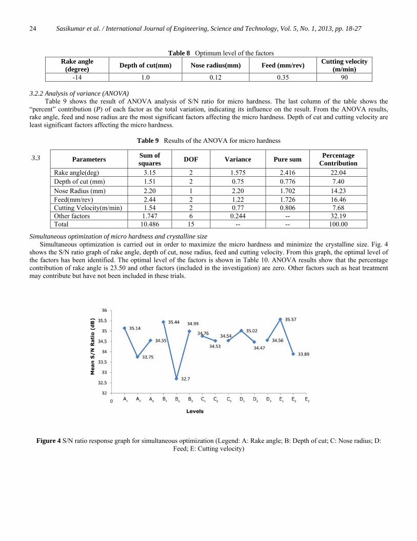
Table 8 Optimum level of the factors Rake angle
(degree) Depth of cut(mm) Nose radius(mm) Feed (mm/rev) Cutting velocity (m/min)
-14 1.0 0.12 0.35 90 3.2.2 Analysis of variance (ANOVA) Table 9 shows the result of ANOVA analysis of S/N ratio for micro hardness. The last column of the table shows the “percent” contribution (P) of each factor as the total variation, indicating its influence on the result. From the ANOVA results, rake angle, feed and nose radius are the most significant factors affecting the micro hardness. Depth of cut and cutting velocity are least significant factors affecting the micro hardness.
Table 9 Results of the ANOVA for micro hardness
3.3
Simultaneous optimization of micro hardness and crystalline size Simultaneous optimization is carried out in order to maximize the micro hardness and minimize the crystalline size. Fig. 4 shows the S/N ratio graph of rake angle, depth of cut, nose radius, feed and cutting velocity. From this graph, the optimal level of the factors has been identified. The optimal level of the factors is shown in Table 10. ANOVA results show that the percentage contribution of rake angle is 23.50 and other factors (included in the investigation) are zero. Other factors such as heat treatment may contribute but have not been included in these trials.
Figure 4 S/N ratio response graph for simultaneous optimization (Legend: A: Rake angle; B: Depth of cut; C: Nose radius; D:
Feed; E: Cutting velocity)
Parameters Sum of squares DOF Variance Pure sum Percentage
Contribution Rake angle(deg) 3.15 2 1.575 2.416 22.04 Depth of cut (mm) 1.51 2 0.75 0.776 7.40 Nose Radius (mm) 2.20 1 2.20 1.702 14.23 Feed(mm/rev) 2.44 2 1.22 1.726 16.46 Cutting Velocity(m/min) 1.54 2 0.77 0.806 7.68 Other factors 1.747 6 0.244 -- 32.19 Total 10.486 15 -- -- 100.00

Sasikumar et al. / International Journal of Engineering, Science and Technology, Vol. 5, No. 1, 2013, pp. 18-27
25
Table10 Simultaneously optimized level for crystalline size and micro hardness Rake
angle(degree) Depth of cut(mm) Nose radius(mm) Feed(mm/rev) Cutting velocity(m/min)
-6 0.5 0.8 0.35 120 3.4 High energy ball milling The chips that were generated from the simultaneously optimized condition were milled in the high energy ball mill. Taguchi L9 orthogonal array is adopted and the experimental results are shown in Table 11.
Table 11 Experimental results and S/N ratio for crystalline size
Trials
Milling Speed(rpm)
Milling Time(hrs) Ball to Powder ratio
Crystalline size(nm) S/N ratio(dB)
1 300 10 15:1 42.604 32.59 2 300 15 20:1 25.550 28.15 3 300 20 25:1 15.997 24.08 4 350 10 15:1 16.000 24.082 5 350 15 20:1 15.975 24.068 6 350 20 25:1 42.631 32.59 7 400 10 15:1 31.931 30.08 8 400 15 20:1 42.744 32.62 9 400 20 25:1 102.702 40.23
3.4.1 Determination of optimum factor level for minimizing crystalline size Figure 5 shows the S/N ratio response graph for milling time, ball to powder ratio and milling speed. From this graph, the optimal level of the factors has been identified and shown in Table 12.
Figure 5 S/N ratio response graph for crystalline size
(Legend: A: Milling time; B: Ball to powder ratio; C: Milling speed)
Table 12 Optimized condition for milling Milling speed
(rpm) Milling time
(hours) Ball to powder ratio
350 15 25:1 3.4.2 Analysis of variance (ANOVA) Table 13 shows the ANOVA of ball milled SS powder for crystalline size. Based on this analysis, it can be concluded that Milling Speed is the most significant factor affecting the crystalline size whereas Milling Time and BPR are the least significant factors. The powder in which obtained from the specified milling conditions are in nanostructure powders. This nanostructure

Sasikumar et al. / International Journal of Engineering, Science and Technology, Vol. 5, No. 1, 2013, pp. 18-27
26
powders having better hardness and tensile strength than the normal powders. The powders obtained from the optimized milling condition have been characterized using TEM and Laser Particle Analyzer. Figure 6 shows the TEM image. The particle size analysis revealed the average size of the particle to be in the range of 108 µm.
A B
Figure 6 (A) & (B) TEM images of ball milled powders
Table 13 Results of the ANOVA for ball milling
Parameters Sum of squares DOF Variance Pure sum Percentage
Contribution Milling speed (rpm) 12.5 2 6.13 126.54 54.11 Milling time (hours) 28.48 2 14.29 75.65 32.34 BPR 68.74 2 34.37 20.03 8.50 Other factors 136.53 2 28.15 Nil 5.05 Total 233.85 8 Nil Nil 100.00
4. Conclusions Nanocrystalline structure has been obtained in the chips machined under 3D (oblique) cutting conditions where as in existing literatures, the research is based on 2D (orthogonal) cutting conditions which are seldom used in metal cutting industries. SPD methods such as Equal Channel Pressing (ECAP), Equal Channel Angular Extrusion (ECAE) and High-Pressure Torsional straining (HPT) are producing Nanostructured materials. However, these methods require multistage deformation which makes them cumbersome and expensive for large volume production. In manufacturing industries, specifically, machine shops generate huge volume of chips that are usually scrapped and so available at a significantly lower price compared to bulk materials These machined chips could be converted into Nanostructured powders for making the components through powder metallurgy route. So this proposed method would be a low cost method for producing nanostructured materials. From the experience gained and the limitations observed during the study, the following recommendations for possible improvements and further investigations in experimental tests and theoretical analyses can be made.
• An analytical model could be developed using Finite Element Methods (FEM) to predict the crystalline size and microhardness. The results of the model could then be compared with the experimentally determined values which have been published in this thesis.
• The nanocrystalline powders which are generated from the ball mill could be compacted into bulk material using several densification techniques such as Hot Isostatic Process (HIP) and Hot Compaction.
• The nanocrystalline powders produced from the ball milling could be used for preparing the nanofluids and study the characteristics of that fluid.
Acknowledgement The authors thank and acknowledge the financial assistance provided for this project by the Department of Science and Technology, Govt. of India under SERC Fast track project SR/FTP/ETA- 27/2007. The authors are also thankful to the management of Sona College of Technology, Salem for their support and encouragement. The correspondence author thanks the Chairman Dr.P. Selvaraj, Secretary Dr.B. Kaviethra Nandhini, and Principal Dr. A. Pushparaghavan of Selvam College of Technology, Namakkal for encouraging me to continue the research work in the Nanomaterials.

Sasikumar et al. / International Journal of Engineering, Science and Technology, Vol. 5, No. 1, 2013, pp. 18-27
27
References ASM Hand Book. Metallographic and Microstructures, 2004. Vol.09, p.1726 – 1733. Brown T.L., Swaminathan S., Chandrasekhar S., Compton W.D., King A.H., and Trumble K.P. 2002. Low-cost manufacturing
process for nanostructured metals and alloys. J. Materials Research Society, Vol. 17, pp. 2484 – 2486. Cai .J. and Liu Z.Y, 2008. Novel microstructures from severely deformed Al–Ti alloys created by chip formation in machining,
Journal Mater. Sci., Vol. 43, No. 5, pp.7474–7480. Cuility B.D. 2000. Stock SR in elements of X-Ray diffraction, Prentice Hall, Inc., New York, pp.170-173. Koch .C.C 1997. Synthesis of nanostructured materials by mechanical milling: problems and opportunities, NanoStructured
Materials. Vol. 9, No. 7, pp. 13-22. Ravi Shankar R., Verma R., Rao B.C., Chandrasekar S., Compton W.D., King A.H., and Trumble K.P. 2007. Severe plastic
deformation of difficult-to-deform materials at near-ambient temperatures, Metallurgical and Materials Transactions, Vol. 38A, pp.1900- 1905.
Sasikumar R and Arunachalam R.M. 2009.Synthesis of nanostructured aluminum matrix composite (AMC) through machining, Materials Letter, Vol. 63, pp.2426 -2428.
Shankar M.R., Verma R., Rao B.C., Chandrasekar S., Compton W.D., King A.H. 2005. Characteristics of aluminum 6061-T6 deformed to large plastic strains by machining, Materials Science and Engineering, Vol. A 410–411, No. 15, pp.364–368.
Swaminathan S, Ravi Shankar M., Rao B.C., Compton W.D., Chandrasekar S., King A.H. and Trumble K.P. 2007. Severe plastic deformation (SPD) and nanostructured materials by machining, Journal of Material Science, Vol. 42, pp.1529–1541.
Swaminathan S., Ravi Shankar M., Lee S., Hwang J., King A.H., Kezar R.F., Rao B.C., Brown T.L., Chandrasekar S., Compton W.D. and Trumble K.P. 2005. Large strain deformation and ultra-fine grained materials by machining, J. Materials Science and Engineering, A 410 – 411, pp.358 – 363.
Suryanarayana C. 2001. Mechanical alloying and milling progress, Materials Science, Vol. 46, pp.1-184. Suryanarayana C., Ivanov E. and Boldyrev V.V. 2001. The science and technology of mechanical alloying, Materials Science and
Engineering Vol. A 304, No. 1-2, pp.151-158. Biographical notes:
Dr. R. Sasikumar received M.E and PhD. Degree from Anna University Chennai. He has been working in various self-financing engineering colleges at various capacities in India. Since 2007, he has been doing his research in the area of Nanomaterials. He has published two research papers in refereed journals and presented two International conferences in the Nanomaterials area.
Professor R.M. Arunachalam, PhD, has obtained Bachelor degree in Mechanical Engineering at Annamalai University, Chidambaram, Tamilnadu, India then he did M.S by research and Ph.D in the specialization of Manufacturing Engineering at National University of Singapore (NUS), Singapore. Since 2003. He has been working as a Professor and Head, Centre for Nanomaterials/ Micromachining at Sona College of Technology, Salem, Tamilnadu, India. He has got Young Scientist Award in the year 2008 from All India Council for Technical Education (AICTE), New Delhi and also he received various research grant worth of forty lakhs INR from different India Government agencies such as Department of Science and Technology (DST), AICTE etc. Professor N. Srinivasa Gupta has obtained Bachelor degree in Mechanical Engineering at Madras University, Chennai, India and then he did M.Tech in Industrial Engineering at Indian Institute of Technology (IIT), Chennai, India. Since 2004, he has been working as an Assistant Professor in the deemed university at India. Received October 2012 Accepted October 2012 Final acceptance in revised form October 2012